US6501284B1 - Capacitive finger detection for fingerprint sensor - Google Patents
Capacitive finger detection for fingerprint sensor Download PDFInfo
- Publication number
- US6501284B1 US6501284B1 US09/648,968 US64896800A US6501284B1 US 6501284 B1 US6501284 B1 US 6501284B1 US 64896800 A US64896800 A US 64896800A US 6501284 B1 US6501284 B1 US 6501284B1
- Authority
- US
- United States
- Prior art keywords
- detection device
- fingerprint detection
- frequency
- capacitive
- finger
- Prior art date
- Legal status (The legal status is an assumption and is not a legal conclusion. Google has not performed a legal analysis and makes no representation as to the accuracy of the status listed.)
- Expired - Lifetime
Links
Images


Classifications
-
- G—PHYSICS
- G06—COMPUTING; CALCULATING OR COUNTING
- G06V—IMAGE OR VIDEO RECOGNITION OR UNDERSTANDING
- G06V40/00—Recognition of biometric, human-related or animal-related patterns in image or video data
- G06V40/10—Human or animal bodies, e.g. vehicle occupants or pedestrians; Body parts, e.g. hands
- G06V40/12—Fingerprints or palmprints
- G06V40/13—Sensors therefor
- G06V40/1306—Sensors therefor non-optical, e.g. ultrasonic or capacitive sensing
-
- G—PHYSICS
- G06—COMPUTING; CALCULATING OR COUNTING
- G06V—IMAGE OR VIDEO RECOGNITION OR UNDERSTANDING
- G06V40/00—Recognition of biometric, human-related or animal-related patterns in image or video data
- G06V40/40—Spoof detection, e.g. liveness detection
Definitions
- the present invention relates to fingerprint detection and recognition and in particular to finger detection within integrated circuit devices employed for fingerprint-based identification and security mechanisms.
- Fingerprint detection and recognition has become a widely implemented identification and security (verification) measure for a variety of applications, including credit card usage, governmental licensing and registration, and premises access control.
- Integrated circuit fingerprint sensors used in such detection usually contain a two-dimensional array of sensing electrodes at a pitch substantially smaller than the size of the lines on the skin surface of a fingertip, allowing an image of the fingerprint pattern to be acquired for processing, analysis and comparison.
- Fingerprint sensor 402 includes a planar array of sensing electrodes 404 conductively coupled to detection and image capture circuitry (not shown). Sensing electrodes 404 may be covered by a protective layer 406 against which the skin surface 408 of the fingertip is placed. Ridges 410 and valleys 412 formed by the lines on the fingertip skin surface 408 are then detected utilizing sensing electrodes 404 .
- Fingerprint detection is most commonly achieved at least partially through capacitive coupling with the finger.
- skin surface 408 and sensing electrodes 404 each form a capacitor having a capacitance proportional to the distance between a respective sensing electrode 404 and the overlying skin surface 408 .
- the capacitance measured by sensor 402 at a point near the top of a fingerprint ridge 410 by a sensing electrode separated from skin surface 408 by a distance d x,y will differ from the capacitance measured through another sensing electrode at a point near the bottom of a fingerprint valley 412 , where the intervening distance d x,y+2 is greater. In this manner an electronic image of the fingerprint may be captured for further processing.
- Fingerprint detection normally involves a relative or comparative process, in which a characteristic such as capacitance) at one sensing electrode within the array is processed relative to similar measurements by the other sensing electrodes.
- the fingerprint sensor is subject to attack by “spoofing,” or presentation of the appropriate fingerprint pattern by an unauthorized individual.
- spoofing the simplest spoofing technique might involve use of a finger severed from an authorized individual for that purpose.
- finger detection is provided by a capacitive grid overlying the fingerprint sensor electrodes to measure the absolute capacitance of the finger placed on the sensor surface.
- the capacitive measurement is converted to a representative frequency, which is then compared to a reference frequency or frequency range to determine whether the measured capacitance matches the expected bio-characteristics of living skin tissue.
- the finger detection thus provides anti-spoofing protection for the fingerprint detection device.
- FIG. 1 depicts a fingerprint sensor circuit employing capacitive finger detection in accordance with a preferred embodiment of the present invention
- FIGS. 2A-2C are cross-sections of fingerprint sensor arrays including capacitive finger detection in accordance with a preferred embodiment of the present invention
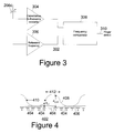
- FIG. 3 depicts a circuit diagram for a finger detection circuit employed within a fingerprint sensor in accordance with a preferred embodiment of the present invention.
- FIG. 4 is a diagram of a known capacitive fingerprint detection structure.
- FIG. 1 depicts a block diagram of the sensor circuit 102 , which is formed as an integrated circuit on a single die.
- a suitable sensor circuit 102 and its operation are described more fully in commonly assigned, copending application Ser. No. 09/040,261, entitled “CAPACITIVE DISTANCE SENSOR” and filed May 9, 1998, which is incorporated herein by reference.
- Sensor circuit 102 includes I 2 C interface and control device 104 , which provides a bidirectional communication protocol enabling sensor circuit 102 to communicate with a controller, such as a microcontroller. I 2 C interface and control device 104 exchanges digital signals via control line 106 with controller circuitry (not shown) external to sensor circuit 102 in the example illustrated, although alternatively such control circuitry may also be integrated within sensor circuit 102 .
- Sensor circuit 102 also includes an array 108 of capacitive sensors for fingerprint acquisition by sensing distances between capacitive electrodes within the sensor array 108 and ridges and grooves on a finger placed in contact with sensor array 108 .
- Sensor array 108 is coupled to the external controller circuit via synchronization line 110 .
- sensor array 108 provides synchronization signals allowing detected voltages representative of the capacitive value of individual capacitive electrodes within sensor array 108 , and therefore representative of the distance between the capacitive electrode and the portion of the epidermal layer contacting sensor array 108 in the region of the capacitive electrode, to be properly interpreted by the external controller.
- Sensor circuit 102 also includes an analog-to-digital (A/D) converter 112 processing analog voltage measurements received from sensor array 108 and generating digital representations recognized by the external controller as distance measurements of the analog-measured voltages from individual capacitive electrodes within sensor array 108 .
- A/D converter 112 transmits these digital signals to the external controller on output bus 114 .
- Sensor array 108 includes a plurality of cells 116 each containing one or more capacitive electrodes.
- Sensor array 108 in the exemplary embodiment contains square cells approximately 45-50 ⁇ m on a side, forming a 250 ⁇ 350 array of contiguous cells 116 within sensor array 108 .
- Sensor array 108 is covered by a passivation material overlying the capacitive electrodes within each cell 116 .
- Other active devices required to form sensor circuit 102 are formed below the capacitive electrodes.
- FIGS. 2A through 2C cross-sections of sensor arrays including capacitive finger detection in accordance with a preferred embodiment of the present invention are illustrated.
- the cross-section depicted in FIGS. 2A and 2B are cross-sections of sensor array 108 taken at section line A—A depicted in FIG. 1 .
- Cells 116 within sensor array 108 each include at least one capacitive fingerprint sensor electrode 202 , which is employed to detect the fingerprint in accordance with the known art.
- a protective layer 204 which may be a combination of insulating and passivating layers, overlies the fingerprint sensor electrodes 202 and provides a surface on which the finger is placed.
- sensor array 108 also includes an array of finger detection sensor electrodes 206 a - 206 b and 206 d. Finger detection sensor electrodes 206 a - 206 b and 206 d are employed to sense the overall capacitance of the finger when placed on the surface of the sensor array 108 . This overall capacitance is then compared to a predefined “sample” or threshold value or range. If the capacitance of the finger is greater than the predefined value (or within the range), a finger is detected on the surface of sensor array 108 .
- Capacitive fingerprint sensor electrodes 202 could be utilized for measuring total capacitance of the finger as well as localized capacitance for detecting fingerprint lines. However, such a design would unnecessarily complicate calculation of capacitances. Instead, separate sensor electrodes 206 a - 206 c, distinct from the capacitive fingerprint sensor electrodes 202 employed to detect the fingerprint, should preferably be employed for capacitive finger detection in accordance with the present invention. Finger detection sensor electrodes may replace the fingerprint detection sensor electrode within a particular cell, as illustrated by sensor electrode 206 a, or may be situated between fingerprint detection sensor electrodes 202 , as illustrated by sensor electrode 206 b.
- a separate, isolated capacitive grid 206 b is formed over the fingerprint sensor detection electrodes 202 .
- Grid lines for the capacitive sensor grid 206 b may be formed within the protective layer 204 over spaces between fingerprint sensor detection electrodes 202 as shown in FIG. 2 A.
- a single capacitive plate 206 d may be formed within the protective layer 204 as shown in FIG. 2B or above the protective layer 204 as shown in FIG. 2C, serving as the capacitive grid. Placement of the finger directly on capacitive plate 206 d will still provide a capacitance for measurement and comparison.
- finger detection sensor electrode(s) 206 a or 206 d, capacitive grid 206 b or capacitive plate 206 d are coupled to a capacitance-to-frequency converter 304 .
- the absolute capacitance of a finger placed on the sensor device 102 is measured and utilized to detect a finger.
- This absolute capacitance will depend on the geometry of the contact area and on the bio-characteristics of the skin on the finger. The impact of differing contact geometries may be minimized by limited the size of the finger detection capacitive grid to an area which will normally be completely covered by the finger.
- the impact of the bio-characteristics of the finger for a living person are employed to prevent spoofing by determining whether the finger placed on the fingerprint sensor device 102 provides a capacitance within a predefined range or above a predefined value.
- the capacitance measurement is accomplished by connecting the variable capacitance representing the finger detection electrode 206 d and the finger to a capacitance-to-frequency converter 304 , which generates different frequencies depending upon the value of the capacitance measured.
- the frequency output of converter 304 which is a function of the capacitance being measured, is compared to at least one fixed-value reference frequency generated by a stable oscillator 306 .
- the difference in frequencies is determined by a frequency comparator 308 , which generates an output signal 310 indicated whether a finger has been detected.
- the measured capacitance may be compared to absolute thresholds or ranges for the entire populace, or to specific ranges for particular individuals identified by their fingerprint, with the individual ranges of authorized individuals being dynamically updated over time to accommodate aging and seasonal variations in the relevant bio-characteristics.
- fingerprint acquisition by the fingerprint sensor may also be concurrently triggered by the finger detection mechanism of the present invention.
- the present invention employs measurement of bio-characteristics of skin, specifically absolute capacitance of a finger placed on a sensor for fingerprint detection, to provide anti-spoofing protection and real finger detection. Other bio-characteristics of living skin tissue may also be employed in conjunction with the present invention.
- the capacitive finger detection mechanism may be combined with the resistive finger detection mechanism described in the related application, either utilizing separate capacitive and resistive grids or utilizing a single grid for both capacitive and resistive measurements.
Abstract
Description
Claims (21)
Priority Applications (4)
| Application Number | Priority Date | Filing Date | Title |
|---|---|---|---|
| US09/648,968 US6501284B1 (en) | 2000-08-28 | 2000-08-28 | Capacitive finger detection for fingerprint sensor |
| EP01306972A EP1187056B1 (en) | 2000-08-28 | 2001-08-16 | Capacitive finger detection for fingerprint sensor |
| DE60124470T DE60124470T2 (en) | 2000-08-28 | 2001-08-16 | Capacitive finger detection in a fingerprint sensor |
| JP2001257286A JP2002112980A (en) | 2000-08-28 | 2001-08-28 | Capacitive finger detection for fingerprint sensor |
Applications Claiming Priority (1)
| Application Number | Priority Date | Filing Date | Title |
|---|---|---|---|
| US09/648,968 US6501284B1 (en) | 2000-08-28 | 2000-08-28 | Capacitive finger detection for fingerprint sensor |
Publications (1)
| Publication Number | Publication Date |
|---|---|
| US6501284B1 true US6501284B1 (en) | 2002-12-31 |
Family
ID=24602957
Family Applications (1)
| Application Number | Title | Priority Date | Filing Date |
|---|---|---|---|
| US09/648,968 Expired - Lifetime US6501284B1 (en) | 2000-08-28 | 2000-08-28 | Capacitive finger detection for fingerprint sensor |
Country Status (4)
| Country | Link |
|---|---|
| US (1) | US6501284B1 (en) |
| EP (1) | EP1187056B1 (en) |
| JP (1) | JP2002112980A (en) |
| DE (1) | DE60124470T2 (en) |
Cited By (25)
| Publication number | Priority date | Publication date | Assignee | Title |
|---|---|---|---|---|
| US6665428B1 (en) * | 2000-08-28 | 2003-12-16 | Stmicroelectronics, Inc. | Resistive finger detection for fingerprint sensor |
| US6693441B2 (en) * | 2001-11-30 | 2004-02-17 | Stmicroelectronics, Inc. | Capacitive fingerprint sensor with protective coating containing a conductive suspension |
| US20040213440A1 (en) * | 2003-04-25 | 2004-10-28 | In-Soo Joo | Apparatus for recognizing an image |
| US20040229681A1 (en) * | 2003-05-12 | 2004-11-18 | Romano James P. | Apparatus and method for generating numbers |
| US20050194959A1 (en) * | 2004-03-04 | 2005-09-08 | Zircon Corporation | Ratiometric stud sensing |
| US20050253597A1 (en) * | 2004-05-14 | 2005-11-17 | Zircon Corporation | Auto-deep scan for capacitive sensing |
| US20050259850A1 (en) * | 2003-08-26 | 2005-11-24 | Toshishige Shimamura | Surface shape recognition sensor |
| US20060034493A1 (en) * | 2003-08-15 | 2006-02-16 | Toshishige Shimamura | Organism recognition system |
| US20060273806A1 (en) * | 2004-02-17 | 2006-12-07 | Gustav Magenwirth Gmbh & Co. Kg | Operator sensing circuit for disabling motor of power equipment |
| US20090232367A1 (en) * | 2004-01-13 | 2009-09-17 | Fujitsu Limited | Identifying device by biometrics information |
| US20090278655A1 (en) * | 2008-05-06 | 2009-11-12 | The Abraham Joshua Heschel School | Method for inhibiting egress from a chamber containing contaminants |
| US20100039121A1 (en) * | 2008-08-15 | 2010-02-18 | Iliev Simeon K | Low cost fingerprint sensor system |
| US7697729B2 (en) | 2004-01-29 | 2010-04-13 | Authentec, Inc. | System for and method of finger initiated actions |
| US7738681B1 (en) | 2005-11-01 | 2010-06-15 | Hewlett-Packard Development Company, L.P. | Fingerprint and physical attribute detection |
| US7831070B1 (en) | 2005-02-18 | 2010-11-09 | Authentec, Inc. | Dynamic finger detection mechanism for a fingerprint sensor |
| US20110050256A1 (en) * | 2009-08-31 | 2011-03-03 | Joachim Frangen | Sensor system for monitoring surroundings on a mechanical component and a method for activating and evaluating the sensor system |
| US8421890B2 (en) | 2010-01-15 | 2013-04-16 | Picofield Technologies, Inc. | Electronic imager using an impedance sensor grid array and method of making |
| US8724038B2 (en) | 2010-10-18 | 2014-05-13 | Qualcomm Mems Technologies, Inc. | Wraparound assembly for combination touch, handwriting and fingerprint sensor |
| US8791792B2 (en) | 2010-01-15 | 2014-07-29 | Idex Asa | Electronic imager using an impedance sensor grid array mounted on or about a switch and method of making |
| US8866347B2 (en) | 2010-01-15 | 2014-10-21 | Idex Asa | Biometric image sensing |
| US9024910B2 (en) | 2012-04-23 | 2015-05-05 | Qualcomm Mems Technologies, Inc. | Touchscreen with bridged force-sensitive resistors |
| US9798917B2 (en) | 2012-04-10 | 2017-10-24 | Idex Asa | Biometric sensing |
| US9864895B1 (en) * | 2016-07-07 | 2018-01-09 | Fingerprint Cards Ab | Fingerprint sensing system with finger detect |
| US9990529B2 (en) | 2013-12-30 | 2018-06-05 | Byd Company Limited | Sensor for detecting fingerprint and identification apparatus and controlling method of sensor for detecting fingerprint |
| US10102411B2 (en) * | 2017-01-25 | 2018-10-16 | Synaptics Incorporated | Hybrid optical and capacitive sensor |
Families Citing this family (8)
| Publication number | Priority date | Publication date | Assignee | Title |
|---|---|---|---|---|
| TWI243339B (en) | 2002-03-19 | 2005-11-11 | Casio Computer Co Ltd | Image reading apparatus and drive control method |
| FR2849244B1 (en) * | 2002-12-20 | 2006-03-10 | Sagem | METHOD FOR DETERMINING THE LIVING CHARACTER OF A CARRIER COMPONENT OF A DIGITAL IMPRINT |
| CN100524344C (en) * | 2003-08-26 | 2009-08-05 | 日本电信电话株式会社 | Surface shape recognition sensor |
| SE1351489A1 (en) * | 2013-12-12 | 2015-06-13 | Fingerprint Cards Ab | Fingerprint detection system and method |
| US20160246396A1 (en) * | 2015-02-20 | 2016-08-25 | Qualcomm Incorporated | Interactive touchscreen and sensor array |
| US9589171B1 (en) * | 2015-10-02 | 2017-03-07 | Fingerprint Cards Ab | Method and device for detecting if a finger is present and sensing a fingerprint pattern |
| US9811708B2 (en) * | 2015-10-02 | 2017-11-07 | Fingerprint Cards Ab | Method and fingerprint sensing device with finger lost detection |
| CN105488464B (en) | 2015-11-26 | 2019-02-19 | 小米科技有限责任公司 | Fingerprint identification method and device |
Citations (5)
| Publication number | Priority date | Publication date | Assignee | Title |
|---|---|---|---|---|
| US4209740A (en) * | 1977-04-06 | 1980-06-24 | Societe Nationale Elf Aquitaine (Production) | Detector for locating the interfacial boundary level between two liquids |
| US4935207A (en) * | 1986-04-01 | 1990-06-19 | The Johns Hopkins University | Capacitive chemical sensor using an ion exchange surface |
| US5673041A (en) * | 1994-03-30 | 1997-09-30 | Chatigny; Joseph Victor | Reflective mode ultrasonic touch sensitive switch |
| US6016355A (en) * | 1995-12-15 | 2000-01-18 | Veridicom, Inc. | Capacitive fingerprint acquisition sensor |
| US6114862A (en) * | 1996-02-14 | 2000-09-05 | Stmicroelectronics, Inc. | Capacitive distance sensor |
Family Cites Families (11)
| Publication number | Priority date | Publication date | Assignee | Title |
|---|---|---|---|---|
| GB2009427B (en) * | 1977-12-01 | 1982-06-09 | Smiths Industries Ltd | Capacitance to frequency conversion means |
| JPH021243A (en) * | 1988-06-08 | 1990-01-05 | Nec Corp | Method and apparatus for detecting forged fingerprint |
| HU214533B (en) * | 1995-10-06 | 1998-03-30 | Dermo Corporation Ltd. | Detector for identifying living character of a finger |
| JP3620558B2 (en) * | 1996-12-16 | 2005-02-16 | ソニー株式会社 | Living body detection device |
| JP2962274B2 (en) * | 1997-04-18 | 1999-10-12 | 日本電気株式会社 | Biological identification method and device |
| US5953441A (en) * | 1997-05-16 | 1999-09-14 | Harris Corporation | Fingerprint sensor having spoof reduction features and related methods |
| JP4013089B2 (en) * | 1997-10-23 | 2007-11-28 | ソニー株式会社 | Fingerprint verification device |
| JPH11185020A (en) * | 1997-12-25 | 1999-07-09 | Glory Ltd | Individual authentication sensor |
| DE19830830C2 (en) * | 1998-07-09 | 2000-11-23 | Siemens Ag | Process for the live detection of human skin |
| DE19836770C1 (en) * | 1998-08-13 | 2000-04-20 | Siemens Ag | Capacitive image capture method |
| JP2000172833A (en) * | 1998-12-10 | 2000-06-23 | Omron Corp | Finger print collating device |
-
2000
- 2000-08-28 US US09/648,968 patent/US6501284B1/en not_active Expired - Lifetime
-
2001
- 2001-08-16 DE DE60124470T patent/DE60124470T2/en not_active Expired - Lifetime
- 2001-08-16 EP EP01306972A patent/EP1187056B1/en not_active Expired - Lifetime
- 2001-08-28 JP JP2001257286A patent/JP2002112980A/en active Pending
Patent Citations (5)
| Publication number | Priority date | Publication date | Assignee | Title |
|---|---|---|---|---|
| US4209740A (en) * | 1977-04-06 | 1980-06-24 | Societe Nationale Elf Aquitaine (Production) | Detector for locating the interfacial boundary level between two liquids |
| US4935207A (en) * | 1986-04-01 | 1990-06-19 | The Johns Hopkins University | Capacitive chemical sensor using an ion exchange surface |
| US5673041A (en) * | 1994-03-30 | 1997-09-30 | Chatigny; Joseph Victor | Reflective mode ultrasonic touch sensitive switch |
| US6016355A (en) * | 1995-12-15 | 2000-01-18 | Veridicom, Inc. | Capacitive fingerprint acquisition sensor |
| US6114862A (en) * | 1996-02-14 | 2000-09-05 | Stmicroelectronics, Inc. | Capacitive distance sensor |
Cited By (49)
| Publication number | Priority date | Publication date | Assignee | Title |
|---|---|---|---|---|
| US6665428B1 (en) * | 2000-08-28 | 2003-12-16 | Stmicroelectronics, Inc. | Resistive finger detection for fingerprint sensor |
| US6693441B2 (en) * | 2001-11-30 | 2004-02-17 | Stmicroelectronics, Inc. | Capacitive fingerprint sensor with protective coating containing a conductive suspension |
| US7369690B2 (en) * | 2003-04-25 | 2008-05-06 | Samsung Electronics Co., Ltd. | Apparatus for recognizing an image |
| US20040213440A1 (en) * | 2003-04-25 | 2004-10-28 | In-Soo Joo | Apparatus for recognizing an image |
| US20040229681A1 (en) * | 2003-05-12 | 2004-11-18 | Romano James P. | Apparatus and method for generating numbers |
| US9028320B2 (en) | 2003-05-12 | 2015-05-12 | James P. Romano | Apparatus and method for generating numbers |
| US7548636B2 (en) * | 2003-08-15 | 2009-06-16 | Nippon Telegraph And Telephone Corporation | Organism recognition system |
| US20060034493A1 (en) * | 2003-08-15 | 2006-02-16 | Toshishige Shimamura | Organism recognition system |
| US20050259850A1 (en) * | 2003-08-26 | 2005-11-24 | Toshishige Shimamura | Surface shape recognition sensor |
| US7366332B2 (en) * | 2003-08-26 | 2008-04-29 | Nippon Telegraph And Telephone Corporation | Surface shape recognition sensor |
| US20080187192A1 (en) * | 2003-08-26 | 2008-08-07 | Toshishige Shimamura | Surface shape recognition sensor device |
| US7508963B2 (en) * | 2003-08-26 | 2009-03-24 | Nippon Telegraph And Telephone Corporation | Surface shape recognition sensor device |
| US7689013B2 (en) | 2004-01-13 | 2010-03-30 | Fujitsu Limited | Identifying device by biometrics information |
| US20090232367A1 (en) * | 2004-01-13 | 2009-09-17 | Fujitsu Limited | Identifying device by biometrics information |
| US7697729B2 (en) | 2004-01-29 | 2010-04-13 | Authentec, Inc. | System for and method of finger initiated actions |
| US20060273806A1 (en) * | 2004-02-17 | 2006-12-07 | Gustav Magenwirth Gmbh & Co. Kg | Operator sensing circuit for disabling motor of power equipment |
| US7795882B2 (en) * | 2004-02-17 | 2010-09-14 | Gustav Magenwirth Gmbh & Co. Kg | Operator sensing circuit for disabling motor of power equipment |
| US7116091B2 (en) | 2004-03-04 | 2006-10-03 | Zircon Corporation | Ratiometric stud sensing |
| US20050194959A1 (en) * | 2004-03-04 | 2005-09-08 | Zircon Corporation | Ratiometric stud sensing |
| US20050253597A1 (en) * | 2004-05-14 | 2005-11-17 | Zircon Corporation | Auto-deep scan for capacitive sensing |
| US7148703B2 (en) * | 2004-05-14 | 2006-12-12 | Zircon Corporation | Auto-deep scan for capacitive sensing |
| US7831070B1 (en) | 2005-02-18 | 2010-11-09 | Authentec, Inc. | Dynamic finger detection mechanism for a fingerprint sensor |
| US7738681B1 (en) | 2005-11-01 | 2010-06-15 | Hewlett-Packard Development Company, L.P. | Fingerprint and physical attribute detection |
| US20090278655A1 (en) * | 2008-05-06 | 2009-11-12 | The Abraham Joshua Heschel School | Method for inhibiting egress from a chamber containing contaminants |
| US20100039121A1 (en) * | 2008-08-15 | 2010-02-18 | Iliev Simeon K | Low cost fingerprint sensor system |
| US8149001B2 (en) * | 2008-08-15 | 2012-04-03 | Standard Microsystems Corporation | Low cost fingerprint sensor system |
| US20110050256A1 (en) * | 2009-08-31 | 2011-03-03 | Joachim Frangen | Sensor system for monitoring surroundings on a mechanical component and a method for activating and evaluating the sensor system |
| US8653837B2 (en) * | 2009-08-31 | 2014-02-18 | Robert Bosch Gmbh | Sensor system for monitoring surroundings on a mechanical component and a method for activating and evaluating the sensor system |
| US9600704B2 (en) | 2010-01-15 | 2017-03-21 | Idex Asa | Electronic imager using an impedance sensor grid array and method of making |
| US11080504B2 (en) | 2010-01-15 | 2021-08-03 | Idex Biometrics Asa | Biometric image sensing |
| US8791792B2 (en) | 2010-01-15 | 2014-07-29 | Idex Asa | Electronic imager using an impedance sensor grid array mounted on or about a switch and method of making |
| US8866347B2 (en) | 2010-01-15 | 2014-10-21 | Idex Asa | Biometric image sensing |
| US10592719B2 (en) | 2010-01-15 | 2020-03-17 | Idex Biometrics Asa | Biometric image sensing |
| US8421890B2 (en) | 2010-01-15 | 2013-04-16 | Picofield Technologies, Inc. | Electronic imager using an impedance sensor grid array and method of making |
| US10115001B2 (en) | 2010-01-15 | 2018-10-30 | Idex Asa | Biometric image sensing |
| US9659208B2 (en) | 2010-01-15 | 2017-05-23 | Idex Asa | Biometric image sensing |
| US9268988B2 (en) | 2010-01-15 | 2016-02-23 | Idex Asa | Biometric image sensing |
| US8743082B2 (en) | 2010-10-18 | 2014-06-03 | Qualcomm Mems Technologies, Inc. | Controller architecture for combination touch, handwriting and fingerprint sensor |
| US8724038B2 (en) | 2010-10-18 | 2014-05-13 | Qualcomm Mems Technologies, Inc. | Wraparound assembly for combination touch, handwriting and fingerprint sensor |
| US9798917B2 (en) | 2012-04-10 | 2017-10-24 | Idex Asa | Biometric sensing |
| US10088939B2 (en) | 2012-04-10 | 2018-10-02 | Idex Asa | Biometric sensing |
| US10101851B2 (en) | 2012-04-10 | 2018-10-16 | Idex Asa | Display with integrated touch screen and fingerprint sensor |
| US10114497B2 (en) | 2012-04-10 | 2018-10-30 | Idex Asa | Biometric sensing |
| US9024910B2 (en) | 2012-04-23 | 2015-05-05 | Qualcomm Mems Technologies, Inc. | Touchscreen with bridged force-sensitive resistors |
| US9990529B2 (en) | 2013-12-30 | 2018-06-05 | Byd Company Limited | Sensor for detecting fingerprint and identification apparatus and controlling method of sensor for detecting fingerprint |
| US9864895B1 (en) * | 2016-07-07 | 2018-01-09 | Fingerprint Cards Ab | Fingerprint sensing system with finger detect |
| US10102411B2 (en) * | 2017-01-25 | 2018-10-16 | Synaptics Incorporated | Hybrid optical and capacitive sensor |
| US20190018998A1 (en) * | 2017-01-25 | 2019-01-17 | Synaptics Incorporated | Hybrid optical and capacitive sensor |
| US10719683B2 (en) * | 2017-01-25 | 2020-07-21 | Fingerprint Cards Ab | Hybrid optical and capacitive sensor |
Also Published As
| Publication number | Publication date |
|---|---|
| DE60124470T2 (en) | 2007-03-01 |
| DE60124470D1 (en) | 2006-12-28 |
| EP1187056A2 (en) | 2002-03-13 |
| JP2002112980A (en) | 2002-04-16 |
| EP1187056A3 (en) | 2004-11-17 |
| EP1187056B1 (en) | 2006-11-15 |
Similar Documents
| Publication | Publication Date | Title |
|---|---|---|
| US6501284B1 (en) | Capacitive finger detection for fingerprint sensor | |
| US6665428B1 (en) | Resistive finger detection for fingerprint sensor | |
| EP1567057B1 (en) | Live finger detection by four-point measurement of complex impedance | |
| US6333989B1 (en) | Contact imaging device | |
| TW303441B (en) | ||
| US7508963B2 (en) | Surface shape recognition sensor device | |
| US7642894B2 (en) | Personal identification apparatus using measured tactile pressure | |
| US7194113B2 (en) | Capacitive biometric sensor | |
| JPH09218006A (en) | Fingerprint sensor | |
| CN107111759A (en) | For detecting whether finger occurs and sense the method and device of fingerprint pattern | |
| US10621323B2 (en) | Biometric authentication apparatus and method | |
| US20070047778A1 (en) | Method and apparatus for asperity detection | |
| US7567690B2 (en) | Method of determining the living character of an element carrying a fingerprint | |
| US11144625B2 (en) | Fingerprint authentication method and system for rejecting spoof attempts | |
| US7657066B2 (en) | Method of determining the living character of an element carrying a fingerprint | |
| US20210081641A1 (en) | Fingerprint authentication method and system for rejecting spoofing attempts | |
| JP3371095B2 (en) | Surface shape recognition sensor | |
| KR20000016679A (en) | Process and system for identification of persons | |
| US11727711B2 (en) | Fingerprint sensing system and method using thresholding | |
| US11062113B2 (en) | Fingerprint authentication system and method providing for reduced latency | |
| KR100641103B1 (en) | Fingerprint sensor of impedance conversion type and fabricating method thereof | |
| KR20030093841A (en) | System and Method of Finger-print Recognition |
Legal Events
| Date | Code | Title | Description |
|---|---|---|---|
| AS | Assignment |
Owner name: STMICROELECTRONICS, INC., TEXAS Free format text: ASSIGNMENT OF ASSIGNORS INTEREST;ASSIGNOR:GOZZINI, GIOVANNI;REEL/FRAME:011054/0327 Effective date: 20000823 |
|
| STCF | Information on status: patent grant |
Free format text: PATENTED CASE |
|
| AS | Assignment |
Owner name: UPEK, INC., CALIFORNIA Free format text: ASSIGNMENT OF ASSIGNORS INTEREST;ASSIGNORS:STMICROELECTRONICS, INC.;STMICROELECTRONICS N.V.;REEL/FRAME:014475/0851 Effective date: 20040304 |
|
| REMI | Maintenance fee reminder mailed | ||
| FPAY | Fee payment |
Year of fee payment: 4 |
|
| SULP | Surcharge for late payment | ||
| FEPP | Fee payment procedure |
Free format text: PAT HOLDER CLAIMS SMALL ENTITY STATUS, ENTITY STATUS SET TO SMALL (ORIGINAL EVENT CODE: LTOS); ENTITY STATUS OF PATENT OWNER: LARGE ENTITY |
|
| FPAY | Fee payment |
Year of fee payment: 8 |
|
| AS | Assignment |
Owner name: AUTHENTEC, INC., FLORIDA Free format text: ASSIGNMENT OF ASSIGNORS INTEREST;ASSIGNOR:UPEK, INC.;REEL/FRAME:026944/0942 Effective date: 20110901 |
|
| FEPP | Fee payment procedure |
Free format text: PAT HOLDER NO LONGER CLAIMS SMALL ENTITY STATUS, ENTITY STATUS SET TO UNDISCOUNTED (ORIGINAL EVENT CODE: STOL); ENTITY STATUS OF PATENT OWNER: LARGE ENTITY |
|
| FPAY | Fee payment |
Year of fee payment: 12 |
|
| AS | Assignment |
Owner name: APPLE INC., CALIFORNIA Free format text: ASSIGNMENT OF ASSIGNORS INTEREST;ASSIGNOR:AUTHENTEC, INC.;REEL/FRAME:035552/0286 Effective date: 20130210 |