US6512281B2 - Method of forming a semiconductor device and an improved deposition system - Google Patents
Method of forming a semiconductor device and an improved deposition system Download PDFInfo
- Publication number
- US6512281B2 US6512281B2 US09/919,389 US91938901A US6512281B2 US 6512281 B2 US6512281 B2 US 6512281B2 US 91938901 A US91938901 A US 91938901A US 6512281 B2 US6512281 B2 US 6512281B2
- Authority
- US
- United States
- Prior art keywords
- layer
- metal
- chamber
- wafer
- barrier
- Prior art date
- Legal status (The legal status is an assumption and is not a legal conclusion. Google has not performed a legal analysis and makes no representation as to the accuracy of the status listed.)
- Expired - Fee Related
Links
- 230000008021 deposition Effects 0.000 title abstract description 73
- 238000000034 method Methods 0.000 title abstract description 30
- 239000004065 semiconductor Substances 0.000 title description 13
- 230000004888 barrier function Effects 0.000 claims abstract description 123
- 229910052751 metal Inorganic materials 0.000 claims abstract description 92
- 239000002184 metal Substances 0.000 claims abstract description 92
- 238000007747 plating Methods 0.000 claims abstract description 50
- 230000002093 peripheral effect Effects 0.000 claims abstract description 35
- 239000000126 substance Substances 0.000 claims abstract description 13
- 239000010410 layer Substances 0.000 claims description 295
- RYGMFSIKBFXOCR-UHFFFAOYSA-N Copper Chemical compound [Cu] RYGMFSIKBFXOCR-UHFFFAOYSA-N 0.000 claims description 106
- 229910052802 copper Inorganic materials 0.000 claims description 106
- 239000010949 copper Substances 0.000 claims description 106
- ATJFFYVFTNAWJD-UHFFFAOYSA-N Tin Chemical compound [Sn] ATJFFYVFTNAWJD-UHFFFAOYSA-N 0.000 claims description 65
- 239000012212 insulator Substances 0.000 claims description 23
- 239000011229 interlayer Substances 0.000 claims description 23
- 238000000151 deposition Methods 0.000 abstract description 92
- XUIMIQQOPSSXEZ-UHFFFAOYSA-N Silicon Chemical compound [Si] XUIMIQQOPSSXEZ-UHFFFAOYSA-N 0.000 description 16
- 229910052710 silicon Inorganic materials 0.000 description 16
- 239000010703 silicon Substances 0.000 description 16
- 238000004544 sputter deposition Methods 0.000 description 15
- 230000008569 process Effects 0.000 description 14
- NRTOMJZYCJJWKI-UHFFFAOYSA-N Titanium nitride Chemical compound [Ti]#N NRTOMJZYCJJWKI-UHFFFAOYSA-N 0.000 description 11
- 238000005137 deposition process Methods 0.000 description 4
- 238000005498 polishing Methods 0.000 description 4
- 238000004140 cleaning Methods 0.000 description 3
- 238000004519 manufacturing process Methods 0.000 description 3
- 230000004048 modification Effects 0.000 description 3
- 238000012986 modification Methods 0.000 description 3
- 230000006872 improvement Effects 0.000 description 2
- RTAQQCXQSZGOHL-UHFFFAOYSA-N Titanium Chemical compound [Ti] RTAQQCXQSZGOHL-UHFFFAOYSA-N 0.000 description 1
- 230000000873 masking effect Effects 0.000 description 1
- 239000010936 titanium Substances 0.000 description 1
- 229910052719 titanium Inorganic materials 0.000 description 1
- WFKWXMTUELFFGS-UHFFFAOYSA-N tungsten Chemical compound [W] WFKWXMTUELFFGS-UHFFFAOYSA-N 0.000 description 1
- 229910052721 tungsten Inorganic materials 0.000 description 1
- 239000010937 tungsten Substances 0.000 description 1
Images


Classifications
-
- H—ELECTRICITY
- H01—ELECTRIC ELEMENTS
- H01L—SEMICONDUCTOR DEVICES NOT COVERED BY CLASS H10
- H01L21/00—Processes or apparatus adapted for the manufacture or treatment of semiconductor or solid state devices or of parts thereof
- H01L21/70—Manufacture or treatment of devices consisting of a plurality of solid state components formed in or on a common substrate or of parts thereof; Manufacture of integrated circuit devices or of parts thereof
- H01L21/71—Manufacture of specific parts of devices defined in group H01L21/70
- H01L21/768—Applying interconnections to be used for carrying current between separate components within a device comprising conductors and dielectrics
- H01L21/76838—Applying interconnections to be used for carrying current between separate components within a device comprising conductors and dielectrics characterised by the formation and the after-treatment of the conductors
- H01L21/76841—Barrier, adhesion or liner layers
- H01L21/76871—Layers specifically deposited to enhance or enable the nucleation of further layers, i.e. seed layers
- H01L21/76873—Layers specifically deposited to enhance or enable the nucleation of further layers, i.e. seed layers for electroplating
-
- H—ELECTRICITY
- H01—ELECTRIC ELEMENTS
- H01L—SEMICONDUCTOR DEVICES NOT COVERED BY CLASS H10
- H01L21/00—Processes or apparatus adapted for the manufacture or treatment of semiconductor or solid state devices or of parts thereof
- H01L21/02—Manufacture or treatment of semiconductor devices or of parts thereof
- H01L21/04—Manufacture or treatment of semiconductor devices or of parts thereof the devices having at least one potential-jump barrier or surface barrier, e.g. PN junction, depletion layer or carrier concentration layer
- H01L21/18—Manufacture or treatment of semiconductor devices or of parts thereof the devices having at least one potential-jump barrier or surface barrier, e.g. PN junction, depletion layer or carrier concentration layer the devices having semiconductor bodies comprising elements of Group IV of the Periodic System or AIIIBV compounds with or without impurities, e.g. doping materials
- H01L21/30—Treatment of semiconductor bodies using processes or apparatus not provided for in groups H01L21/20 - H01L21/26
- H01L21/31—Treatment of semiconductor bodies using processes or apparatus not provided for in groups H01L21/20 - H01L21/26 to form insulating layers thereon, e.g. for masking or by using photolithographic techniques; After treatment of these layers; Selection of materials for these layers
- H01L21/32—Treatment of semiconductor bodies using processes or apparatus not provided for in groups H01L21/20 - H01L21/26 to form insulating layers thereon, e.g. for masking or by using photolithographic techniques; After treatment of these layers; Selection of materials for these layers using masks
-
- C—CHEMISTRY; METALLURGY
- C23—COATING METALLIC MATERIAL; COATING MATERIAL WITH METALLIC MATERIAL; CHEMICAL SURFACE TREATMENT; DIFFUSION TREATMENT OF METALLIC MATERIAL; COATING BY VACUUM EVAPORATION, BY SPUTTERING, BY ION IMPLANTATION OR BY CHEMICAL VAPOUR DEPOSITION, IN GENERAL; INHIBITING CORROSION OF METALLIC MATERIAL OR INCRUSTATION IN GENERAL
- C23C—COATING METALLIC MATERIAL; COATING MATERIAL WITH METALLIC MATERIAL; SURFACE TREATMENT OF METALLIC MATERIAL BY DIFFUSION INTO THE SURFACE, BY CHEMICAL CONVERSION OR SUBSTITUTION; COATING BY VACUUM EVAPORATION, BY SPUTTERING, BY ION IMPLANTATION OR BY CHEMICAL VAPOUR DEPOSITION, IN GENERAL
- C23C14/00—Coating by vacuum evaporation, by sputtering or by ion implantation of the coating forming material
- C23C14/04—Coating on selected surface areas, e.g. using masks
- C23C14/042—Coating on selected surface areas, e.g. using masks using masks
-
- C—CHEMISTRY; METALLURGY
- C23—COATING METALLIC MATERIAL; COATING MATERIAL WITH METALLIC MATERIAL; CHEMICAL SURFACE TREATMENT; DIFFUSION TREATMENT OF METALLIC MATERIAL; COATING BY VACUUM EVAPORATION, BY SPUTTERING, BY ION IMPLANTATION OR BY CHEMICAL VAPOUR DEPOSITION, IN GENERAL; INHIBITING CORROSION OF METALLIC MATERIAL OR INCRUSTATION IN GENERAL
- C23C—COATING METALLIC MATERIAL; COATING MATERIAL WITH METALLIC MATERIAL; SURFACE TREATMENT OF METALLIC MATERIAL BY DIFFUSION INTO THE SURFACE, BY CHEMICAL CONVERSION OR SUBSTITUTION; COATING BY VACUUM EVAPORATION, BY SPUTTERING, BY ION IMPLANTATION OR BY CHEMICAL VAPOUR DEPOSITION, IN GENERAL
- C23C14/00—Coating by vacuum evaporation, by sputtering or by ion implantation of the coating forming material
- C23C14/22—Coating by vacuum evaporation, by sputtering or by ion implantation of the coating forming material characterised by the process of coating
- C23C14/50—Substrate holders
-
- C—CHEMISTRY; METALLURGY
- C23—COATING METALLIC MATERIAL; COATING MATERIAL WITH METALLIC MATERIAL; CHEMICAL SURFACE TREATMENT; DIFFUSION TREATMENT OF METALLIC MATERIAL; COATING BY VACUUM EVAPORATION, BY SPUTTERING, BY ION IMPLANTATION OR BY CHEMICAL VAPOUR DEPOSITION, IN GENERAL; INHIBITING CORROSION OF METALLIC MATERIAL OR INCRUSTATION IN GENERAL
- C23C—COATING METALLIC MATERIAL; COATING MATERIAL WITH METALLIC MATERIAL; SURFACE TREATMENT OF METALLIC MATERIAL BY DIFFUSION INTO THE SURFACE, BY CHEMICAL CONVERSION OR SUBSTITUTION; COATING BY VACUUM EVAPORATION, BY SPUTTERING, BY ION IMPLANTATION OR BY CHEMICAL VAPOUR DEPOSITION, IN GENERAL
- C23C14/00—Coating by vacuum evaporation, by sputtering or by ion implantation of the coating forming material
- C23C14/22—Coating by vacuum evaporation, by sputtering or by ion implantation of the coating forming material characterised by the process of coating
- C23C14/56—Apparatus specially adapted for continuous coating; Arrangements for maintaining the vacuum, e.g. vacuum locks
- C23C14/568—Transferring the substrates through a series of coating stations
-
- C—CHEMISTRY; METALLURGY
- C25—ELECTROLYTIC OR ELECTROPHORETIC PROCESSES; APPARATUS THEREFOR
- C25D—PROCESSES FOR THE ELECTROLYTIC OR ELECTROPHORETIC PRODUCTION OF COATINGS; ELECTROFORMING; APPARATUS THEREFOR
- C25D17/00—Constructional parts, or assemblies thereof, of cells for electrolytic coating
- C25D17/001—Apparatus specially adapted for electrolytic coating of wafers, e.g. semiconductors or solar cells
-
- C—CHEMISTRY; METALLURGY
- C25—ELECTROLYTIC OR ELECTROPHORETIC PROCESSES; APPARATUS THEREFOR
- C25D—PROCESSES FOR THE ELECTROLYTIC OR ELECTROPHORETIC PRODUCTION OF COATINGS; ELECTROFORMING; APPARATUS THEREFOR
- C25D7/00—Electroplating characterised by the article coated
- C25D7/12—Semiconductors
- C25D7/123—Semiconductors first coated with a seed layer or a conductive layer
-
- H—ELECTRICITY
- H01—ELECTRIC ELEMENTS
- H01L—SEMICONDUCTOR DEVICES NOT COVERED BY CLASS H10
- H01L21/00—Processes or apparatus adapted for the manufacture or treatment of semiconductor or solid state devices or of parts thereof
- H01L21/02—Manufacture or treatment of semiconductor devices or of parts thereof
- H01L21/04—Manufacture or treatment of semiconductor devices or of parts thereof the devices having at least one potential-jump barrier or surface barrier, e.g. PN junction, depletion layer or carrier concentration layer
- H01L21/18—Manufacture or treatment of semiconductor devices or of parts thereof the devices having at least one potential-jump barrier or surface barrier, e.g. PN junction, depletion layer or carrier concentration layer the devices having semiconductor bodies comprising elements of Group IV of the Periodic System or AIIIBV compounds with or without impurities, e.g. doping materials
- H01L21/28—Manufacture of electrodes on semiconductor bodies using processes or apparatus not provided for in groups H01L21/20 - H01L21/268
- H01L21/283—Deposition of conductive or insulating materials for electrodes conducting electric current
- H01L21/285—Deposition of conductive or insulating materials for electrodes conducting electric current from a gas or vapour, e.g. condensation
- H01L21/28506—Deposition of conductive or insulating materials for electrodes conducting electric current from a gas or vapour, e.g. condensation of conductive layers
- H01L21/28512—Deposition of conductive or insulating materials for electrodes conducting electric current from a gas or vapour, e.g. condensation of conductive layers on semiconductor bodies comprising elements of Group IV of the Periodic System
- H01L21/2855—Deposition of conductive or insulating materials for electrodes conducting electric current from a gas or vapour, e.g. condensation of conductive layers on semiconductor bodies comprising elements of Group IV of the Periodic System by physical means, e.g. sputtering, evaporation
-
- H—ELECTRICITY
- H01—ELECTRIC ELEMENTS
- H01L—SEMICONDUCTOR DEVICES NOT COVERED BY CLASS H10
- H01L21/00—Processes or apparatus adapted for the manufacture or treatment of semiconductor or solid state devices or of parts thereof
- H01L21/02—Manufacture or treatment of semiconductor devices or of parts thereof
- H01L21/04—Manufacture or treatment of semiconductor devices or of parts thereof the devices having at least one potential-jump barrier or surface barrier, e.g. PN junction, depletion layer or carrier concentration layer
- H01L21/18—Manufacture or treatment of semiconductor devices or of parts thereof the devices having at least one potential-jump barrier or surface barrier, e.g. PN junction, depletion layer or carrier concentration layer the devices having semiconductor bodies comprising elements of Group IV of the Periodic System or AIIIBV compounds with or without impurities, e.g. doping materials
- H01L21/28—Manufacture of electrodes on semiconductor bodies using processes or apparatus not provided for in groups H01L21/20 - H01L21/268
- H01L21/283—Deposition of conductive or insulating materials for electrodes conducting electric current
- H01L21/288—Deposition of conductive or insulating materials for electrodes conducting electric current from a liquid, e.g. electrolytic deposition
- H01L21/2885—Deposition of conductive or insulating materials for electrodes conducting electric current from a liquid, e.g. electrolytic deposition using an external electrical current, i.e. electro-deposition
-
- H—ELECTRICITY
- H01—ELECTRIC ELEMENTS
- H01L—SEMICONDUCTOR DEVICES NOT COVERED BY CLASS H10
- H01L21/00—Processes or apparatus adapted for the manufacture or treatment of semiconductor or solid state devices or of parts thereof
- H01L21/70—Manufacture or treatment of devices consisting of a plurality of solid state components formed in or on a common substrate or of parts thereof; Manufacture of integrated circuit devices or of parts thereof
- H01L21/71—Manufacture of specific parts of devices defined in group H01L21/70
- H01L21/768—Applying interconnections to be used for carrying current between separate components within a device comprising conductors and dielectrics
- H01L21/76838—Applying interconnections to be used for carrying current between separate components within a device comprising conductors and dielectrics characterised by the formation and the after-treatment of the conductors
- H01L21/76841—Barrier, adhesion or liner layers
- H01L21/76843—Barrier, adhesion or liner layers formed in openings in a dielectric
Definitions
- the present invention relates to a method of forming a copper electrode buried in an insulating layer of a semiconductor device free from such a problem that a copper electrode plating layer is peeled thereby educing a yield of a semiconductor device, and more particularly to a method of forming a copper electrode on a copper seed layer on a TiN barrier layer formed in a trench groove and a through hole formed in an inter-layer insulator of a semiconductor device, buried in an insulating layer of a semiconductor device.
- the first present invention provides a multi-layer structure comprising: a barrier layer on a predetermined region of an insulating layer; a metal seed layer made of a metal which is different in substance from the barrier layer, the metal seed layer extending not only on an entire surface of the barrier layer but also a peripheral region positioned outside the predetermined region of the insulating layer; and a metal plating layer made of the metal as the seed layer, and the metal layer being adhered on the metal seed layer so that the metal plating layer is separated from the barrier layer and also from the insulating layer.
- the second present invention provides a method of forming a multi-layer structure over an insulating layer.
- the method comprises the steps of: selectively depositing a barrier layer on a predetermined region of an insulating layer by use of a first deposition mask; selectively depositing a metal seed layer made of a metal which is different in substance from the barrier layer by use of a second deposition mask, so that the metal seed layer extends not only on an entire surface of the barrier layer but also a peripheral region positioned outside the predetermined region of the insulating layer; and forming a metal plating layer made of the same metal as the seed layer, so that the metal plating layer is adhered on the metal seed layer whereby the metal plating layer is separated from the barrier layer and also from the insulating layer.
- the third present invention provides a deposition system for forming a multi-layer structure over an insulating layer.
- the deposition system comprises: a first deposition chamber having a first deposition mask for selectively depositing a barrier layer on a predetermined region of an insulating layer; and a second deposition chamber having a second deposition mask for selectively depositing a metal seed layer made of a metal which is different in substance from the barrier layer, so that the metal seed layer extends not only on an entire surface of the barrier layer but also a peripheral region positioned outside the predetermined region of the insulating layer, wherein the first deposition mask has a first opening edge having a first diameter and the second mask has a second opening edge having a second diameter which is larger than the first diameter of the first deposition mask, whereby a metal plating layer made of the metal as the seed layer is formed on the metal seed layer, wherein the metal plating layer is separated from the barrier layer and also from the insulating layer.
- FIGS. 1A through 1E are fragmentary cross sectional elevation views illustrative of semiconductor devices in sequential steps involved in a novel fabrication method thereof by use of a novel deposition system in accordance with the present invention.
- FIG. 2 is a plane view of a plane layout of a deposition system for depositing a barrier metal layer, a copper seed layer and a copper plating layer in accordance with the present invention.
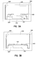
- FIG. 3A is a cross sectional elevation view illustrative of a TiN barrier chamber of a deposition system of FIG. 2 before clamping a wafer in accordance with the present invention.
- FIG. 3B is a cross sectional elevation view illustrative of a TiN barrier chamber of a deposition system of FIG. 2 after having clamped a wafer for a sputtering process for deposition of a titanium nitride layer in accordance with the present invention.
- FIG. 4A is a plane view illustrative of a clamp ring of the damper in the TiN barrier chamber in the deposition chamber of FIGS. 3A and 3B in accordance with the present invention.
- FIG. 4B is a plane view illustrative of a clamp ring of the damper in the copper seed chamber in the deposition chamber of FIGS. 3A and 3B in accordance with the present invention.
- FIG. 5A is a fragmentary cross sectional elevation view illustrative of a deposited TiN barrier layer not only on a wafer but also on a clamp ring after a sputtering process to a wafer in the TiN barrier chamber illustrated in FIG. 3B of the deposition system of FIG. 2 in accordance with the present invention.
- FIG. 5B is a fragmentary cross sectional elevation view illustrative of a deposited copper seed layer not only on a wafer but also on a clamp ring after a sputtering process to a wafer in the copper seed chamber illustrated in FIG. 3B of the deposition system of FIG. 2 in accordance with the present invention.
- FIG. 5C is a fragmentary cross sectional elevation view illustrative of the silicon wafer formed thereon with the copper plating layer in accordance with the present invention.
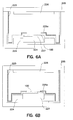
- FIG. 6A is a cross sectional elevation view illustrative of another TiN barrier chamber of a deposition system of FIG. 2 before clamping a wafer in accordance with the present invention.
- FIG. 6B is a cross sectional elevation view illustrative of another TiN barrier chamber of a deposition system of FIG. 2 after having clamped a wafer for a sputtering process for deposition of a titanium nitride layer in accordance with the present invention.
- the first present invention provides a multi-layer structure comprising: a barrier layer on a predetermined region of an insulating layer; a metal seed layer made of a metal which is different in substance from the barrier layer, the metal seed layer extending not only on an entire surface of the barrier layer but also a peripheral region positioned outside the predetermined region of the insulating layer; and a metal plating layer made of the metal as the seed layer, and the metal layer being adhered on the metal seed layer so that the metal plating layer is separated from the barrier layer and also from the insulating layer.
- the barrier layer comprises a TiN barrier layer, and the metal seed layer and the metal plating layer are made of copper.
- the multi-layer structure is formed in at least one of a trench groove in an inter-layer insulator as the insulating layer and a through hole also formed in the inter-layer insulator.
- the second present invention provides a method of forming a multi-layer structure over an insulating layer.
- the method comprises the steps of: selectively depositing a barrier layer on a predetermined region of an insulating layer by use of a first deposition mask; selectively depositing a metal seed layer made of a metal which is different in substance from the barrier layer by use of a second deposition mask, so that the metal seed layer extends not only on an entire surface of the barrier layer but also a peripheral region positioned outside the predetermined region of the insulating layer; and forming a metal plating layer made of the same metal as the seed layer, so that the metal plating layer is adhered on the metal seed layer whereby the metal plating layer is separated from the barrier layer and also from the insulating layer.
- the first deposition mask has a first opening edge having a first diameter and the second mask has a second opening edge having a second diameter which is larger than the first diameter of the first deposition mask.
- the first deposition mask comprises a first clamping ring member with the first opening edge having the first diameter of a first damper for clamping a wafer for a deposition process for selectively depositing the barrier layer on the predetermined region of the insulating layer
- the second deposition mask comprises a second clamping ring member with the second opening edge having the second diameter of a second damper for clamping the wafer for a deposition process for selectively depositing the metal seed layer not only on an entire surface of the barrier layer but also the peripheral region positioned outside the predetermined region of the insulating layer.
- the first deposition mask comprises a first shielding plate extension member extending from a first shielding plate covering an inner wall of a first chamber, and the first shielding plate extension member having the first opening edge having the first diameter for selectively depositing the barrier layer on the predetermined region of the insulating layer
- the second deposition mask comprises a second shielding plate extension member extending from a second shielding plate covering an inner wall of a second chamber, and the second shielding plate extension member having the second opening edge having the second diameter for selectively depositing the metal seed layer not only on an entire surface of the barrier layer but also the peripheral region positioned outside the predetermined region of the insulating layer.
- the barrier layer comprises a TiN barrier layer, and the metal seed layer and the metal plating layer are made of copper.
- the multi-layer structure is formed in at least one of a trench groove in an inter-layer insulator as the insulating layer and a through hole also formed in the inter-layer insulator.
- the third present invention provides a deposition system for forming a multi-layer structure over an insulating layer.
- the deposition system comprises: a first deposition chamber having a first deposition mask for selectively depositing a barrier layer on a predetermined region of an insulating layer; and a second deposition chamber having a second deposition mask for selectively depositing a metal seed layer made of a metal which is different in substance from the barrier layer, so that the metal seed layer extends not only on an entire surface of the barrier layer but also a peripheral region positioned outside the predetermined region of the insulating layer, wherein the first deposition mask has a first opening edge having a first diameter and the second mask has a second opening edge having a second diameter which is larger than the first diameter of the first deposition mask, whereby a metal plating layer made of the metal as the seed layer is formed on the metal seed layer, wherein the metal plating layer is separated from the barrier layer and also from the insulating layer.
- the first deposition mask comprises a first clamping ring member with the first opening edge having the first diameter of a first damper for clamping a wafer for a deposition process for selectively depositing the barrier layer on the predetermined region of the insulating layer
- the second deposition mask comprises a second clamping ring member with the second opening edge having the second diameter of a second damper for clamping the wafer for a deposition process for selectively depositing the metal seed layer not only on an entire surface of the barrier layer but also the peripheral region positioned outside the predetermined region of the insulating layer.
- the first deposition mask comprises a first shielding plate extension member extending from a first shielding plate covering an inner wall of the first deposition chamber, and the first shielding plate extension member having the first opening edge having the first diameter for selectively depositing the barrier layer on the predetermined region of the insulating layer
- the second deposition mask comprises a second shielding plate extension member extending from a second shielding plate covering an inner wall of a second deposition chamber, and the second shielding plate extension member having the second opening edge having the second diameter for selectively depositing the metal seed layer not only on an entire surface of the barrier layer but also the peripheral region positioned outside the predetermined region of the insulating layer.
- the barrier layer comprises a TiN barrier layer, and the metal seed layer is made of copper.
- FIGS. 1A through 1E are fragmentary cross sectional elevation views illustrative of semiconductor devices in sequential steps involved in a novel fabrication method thereof.
- a first trench groove 102 is formed in an upper region of a first inter-layer insulator 101 which is formed over a silicon wafer which is not illustrated.
- a first barrier metal layer 103 is entirely deposited over the first inter-layer insulator 101 and on side walls and a bottom of the first trench groove 102 .
- the first barrier metal layer 103 may comprise a titanium nitride or titanium.
- a first level interconnection layer 104 of tungsten is further deposited on the first barrier metal layer 104 . Those first barrier metal layer 103 and the first level interconnection layer 104 are then subjected to a chemical mechanical polishing method to leave the first barrier metal layer 103 and the first level interconnection layer 104 only within the interconnection trench groove 102 .
- a second inter-layer insulator 105 is formed on the surface of the first inter-layer insulator 101 and on the first level interconnection layer 104 .
- Second trench grooves 106 are formed in upper regions of the second inter-layer insulator 105 .
- a through hole 107 is then formed in the second inter-layer insulator 105 , so that the through hole 107 connects the bottom of the second trench groove and the top surface of the first level interconnection layer 104 , whereby a part of the top surface of the first level interconnection layer 104 is shown through the through hole 107 .
- a second barrier metal layer 108 of titanium nitride is entirely deposited by a sputtering method on a top surface of the second inter-layer insulator 105 and side walls and bottoms of the second trench grooves 106 and on side walls of the through hole 107 as well as on the shown part of the top surface of the first level interconnection layer 104 .
- a copper seed layer 109 is then deposited on the second barrier metal layer 108 by a sputtering method.
- a copper plating layer 110 is then formed on the copper seed layer 109 , so that the copper plating layer 110 is much thicker than the second trench grooves 106 and the through hole 107 , whereby the top surface of the copper seed layer 109 over the top surface of the second inter-layer insulator 105 is completely embedded within the copper plating layer 110 .
- the copper plating layer 110 is then polished by a chemical mechanical polishing method so as to leave the copper plating layer 110 only within the second trench grooves 106 and the through hole 107 thereby forming copper electrodes as second level interconnection layers 111 within the second trench grooves 106 and the through hole 107 .
- FIG. 2 is a plane view of a plane layout of a deposition system for depositing a barrier metal layer, a copper seed layer and a copper plating layer.
- the above fabrication processes of FIGS. 1C and 1D are carried out by use of this deposition system 200 .
- the deposition system 200 has a hexagonal shaped carrier chamber 201 , and first and second load lock chambers 202 and 203 and four vacuum chambers 204 , 205 , 206 and 207 .
- the first load lock chamber 202 serves as a loading chamber for setting a wafer 100 in a cartridge 210 accommodated in the first load lock chamber 202 .
- the second load lock chamber 203 also serves as an unloading chamber for setting the wafer 100 in another cartridge 211 accommodated in the first load lock chamber 203 .
- the first vacuum chamber 204 serves as a cleaning chamber.
- the second vacuum chamber 205 serves as a TiN barrier chamber.
- the third vacuum chamber 206 serves as a copper seed chamber.
- the fourth vacuum chamber 207 serves as a reserve chamber.
- the carrier chamber 201 is positioned in center of the deposition system.
- the two load lock chambers 202 and 203 and the four vacuum chambers 204 , 205 , 206 and 207 are positioned along six sides of the hexagonal shaped carrier chamber 201 .
- the carrier chamber 201 has a handler 208 for carrying the wafer in a clock wise direction.
- the two load lock chambers 202 and 203 and the four vacuum chambers 204 , 205 , 206 and 207 are connected through gates 202 a , 203 a , 204 a , 205 a , 206 a , 206 a , and 207 a to the carrier chamber 201 so that the two load lock chambers 202 and 203 and the four vacuum chambers 204 , 205 , 206 and 207 are kept in vacuum states independently.
- FIG. 3A is a cross sectional elevation view illustrative of a TiN barrier chamber of a deposition system of FIG. 2 before clamping a wafer.
- FIG. 3B is a cross sectional elevation view illustrative of a TiN barrier chamber of a deposition system of FIG. 2 after having clamped a wafer for a sputtering process for deposition of a titanium nitride layer.
- the wafer is mounted on a heat stage 221 accommodated in the TiN barrier chamber 205 .
- a damper 222 is provided around the heat stage for clamping the wafer 100 on the heat stage 221 .
- the damper 222 has a clamp ring 223 and a driver 224 for moving the clamp ring 223 in upward and downward directions for allowing the clamp ring 223 directly clamps or releases the wafer 100 .
- the driver 224 moves the clamp ring 223 in downward direction so that the clamp ring 223 is made into contact with peripheral portions of the wafer 110 for clamping the wafer 110 on the heat stage 221 .
- a titanium nitride target 226 is provided over the heat stage 221 .
- a shield plate 225 is provided on an inner wall of the TiN barrier chamber 205 for preventing sputtered titanium nitride from being adhered onto the inner walls of the chamber.
- FIG 4A is a plane view illustrative of a clamp ring of the damper in the TiN barrier chamber in the deposition chamber of FIGS. 3A and 3B.
- the clamp ring 223 of the damper 222 of the TiN barrier chamber 205 in the deposition chamber has an inner diameter ⁇ W 1 which is smaller than an outer diameter ⁇ W 0 of the wafer 100 .
- the structure of the copper seed chamber 206 is essentially the same as the TiN barrier chamber 205 , for which reason illustrations thereof are omitted.
- the wafer is mounted on a heat stage accommodated in the copper seed chamber 206 .
- a damper is also provided around the heat stage for clamping the wafer on the heat stage.
- the damper has a clamp ring and a driver for moving the clamp ring in upward and downward directions for allowing the clamp ring directly clamps or releases the wafer. When the driver moves the clamp ring in downward direction so that the clamp ring is made into contact with peripheral portions of the wafer for clamping the wafer 110 on the heat stage.
- a copper target is provided over the heat stage.
- FIG. 4B is a plane view illustrative of a clamp ring of the damper in the copper seed chamber in the deposition chamber of FIGS. 3A and 3B.
- the clamp ring of the damper of the copper seed chamber in the deposition chamber has an inner diameter ⁇ W 2 which is smaller than an outer diameter ⁇ W 0 of the wafer 100 but larger than the inner diameter ⁇ W 1 of the clamp ring of the clamp chamber 205 .
- the wafer 100 having set in the first load clock chamber 202 is first carried by the handler 208 into the cleaning chamber 204 for cleaning a surface of the first level interconnection layer by use of a reversed sputtering process utilizing a radio frequency plasma.
- the wafer 100 is then carried by the handler 208 to the TiN barrier chamber 205 .
- the wafer 100 is treated as illustrated in FIGS. 3A and 3B.
- FIG. 5A is a fragmentary cross sectional elevation view illustrative of a deposited TiN barrier layer not only on a wafer but also on a clamp ring after a sputtering process to a wafer in the TiN barrier chamber illustrated in FIG. 3B of the deposition system of FIG. 2 .
- the TiN barrier layer is deposited not only on the silicon wafer 100 but also on the clamping ring 223 . This means that no TiN barrier layer is deposited on the peripheral region of the wafer 100 , and the edge of the TiN barrier layer on the silicon wafer 100 is defined by the edge of the clamping ring 223 .
- the dimension of the peripheral region free of the deposition of the TiN barrier layer 108 is defined by a difference in the inner diameter ⁇ W 1 of the clamping ring 223 of the damper 222 and the outer diameter ⁇ W 0 of the silicon wafer 100 .
- the wafer 100 formed thereon with the TiN barrier layer 108 is then carried by the handler 208 into the copper seed chamber 206 .
- the wafer 100 is treated so that the wafer 100 is mounted in the heat stage to be heated up to a temperature of about 25° C., and also the clamp ring 223 B is moved down to be made into contact with the peripheral portion of the wafer 100 for clamping the wafer 100 onto the heat stage, whereby the copper sputtering process is carried out to deposit the copper seed layer 109 on the TiN barrier layer 108 .
- 5B is a fragmentary cross sectional elevation view illustrative of a deposited copper seed layer not only on a wafer but also on a clamp ring after a sputtering process to a wafer in the copper seed chamber illustrated in FIG. 3B of the deposition system of FIG. 2 . Since the peripheral portion of the wafer 100 is covered by the clamping ring 223 B of the damper 222 B, the copper seed layer 109 is deposited not only on the TiN barrier layer 108 over the silicon wafer 100 but also on the clamping ring 223 B.
- the edge of the copper seed layer 109 is positioned outside the edge of the TiN barrier layer 108 , whereby the copper seed layer 109 is deposited not only on the TiN barrier layer 108 and the clamping ring 223 B of the damper 222 B in the copper seed chamber 206 but also on the silicon wafer 100 in an outside region defined between the inner diameter ⁇ W 2 of the clamping ring 223 B of the copper seed chamber 206 and the inner diameter ⁇ W 1 of the clamping ring 223 of the TiN barrier chamber 205 .
- the TiN barrier layer 108 is completely covered by the copper seed layer 109 .
- the dimension of the outside region of the silicon wafer 100 is defined by the difference in the inner diameter ⁇ W 2 of the clamping ring 223 B of the copper seed layer 109 and the inner diameter ⁇ W 1 of the clamping ring 223 of the TiN barrier layer 205 .
- FIG. 5C is a fragmentary cross sectional elevation view illustrative of the silicon wafer formed thereon with the copper plating layer. Since the TiN barrier layer 108 is completely covered by the copper seed layer 109 , then the copper plating layer 110 is completely separated by the copper seed layer 109 from the TiN barrier layer 108 .
- the copper plating layer 110 , the copper seed layer 109 and the TiN barrier layer 108 are sequentially polished by a chemical and mechanical polishing method so as to leave the copper plating layer 110 , the copper seed layer 109 and the TiN barrier layer 108 only with in the second trench groove and the through hole, whereby the copper electrode 111 is then formed in the second trench groove formed in the second inter-layer insulator.
- the entire parts of the copper plating layer 110 is formed in contact with the surface of the copper seed layer 109 , for which reason the copper plating layer 110 is free from the problem with a possibility of peeling from the wafer 100 . This means that no problem is raised with drop of the yield due to the peeled part of the copper plating layer. Namely, the present invention allows the improvement in the yield of the semiconductor device.
- FIG. 6A is a cross sectional elevation view illustrative of another TiN barrier chamber of a deposition system of FIG. 2 before clamping a wafer.
- FIG. 6B is a cross sectional elevation view illustrative of another TiN barrier chamber of a deposition system of FIG. 2 after having clamped a wafer for a sputtering process for deposition of a titanium nitride layer.
- the copper seed chamber may also be structured as of the TiN barrier chamber.
- the wafer 100 is mounted on a heat stage 221 accommodated in the TiN barrier chamber 205 .
- the wafer 100 is fixed by an electrostatic chuck 227 provided on the heat stage 221 .
- a titanium nitride target 226 is provided over the heat stage 221 .
- a shield plate 225 is provided on an inner wall of the TiN barrier chamber 205 for preventing sputtered titanium nitride from being adhered onto the inner walls of the chamber. No clamper is provided but a sputter mask 225 a is provided which extends from the shield plate 225 so that the sputter mask 225 a is positioned to cover the peripheral region of the wafer 100 , so that no deposition of the TiN barrier layer is made onto the peripheral region of the wafer 100 .
- the heat stage 221 is moved in upward and downward directions by a driver 224 .
- the driver 24 moves the heat stage 221 upwardly so that the peripheral region of the wafer 100 is covered by the sputter mask 225 a extended from the shield plate 225 to prevent the deposition of the TiN barrier layer on the peripheral region of the wafer 110 .
- the sputter mask 225 a is defined by an opening edge thereof which has an inner diameter ⁇ W 1 smaller than the outer diameter ⁇ W 0 of the wafer 100 .
- the copper seed chamber 206 may also be structured as illustrated in FIGS. 6A and 6B.
- the wafer 100 is also mounted on a heat stage accommodated in the copper seed chamber 206 .
- the wafer 100 is fixed by an electrostatic chuck provided on the heat stage.
- a titanium nitride target is provided over the heat stage.
- a shield plate is provided on an inner wall of the copper seed chamber 206 for preventing sputtered copper from being adhered onto the inner walls of the chamber. No damper is provided but a sputter mask is provided which extends from the shield plate so that the sputter mask is positioned to cover the peripheral region of the wafer 100 , so that no deposition of the copper seed layer is made onto the peripheral region of the wafer 100 .
- the heat stage is moved in upward and downward directions by a driver.
- the driver moves the heat stage upwardly so that the peripheral region of the wafer 100 is covered by the sputter mask extended from the shield plate to prevent the deposition of the copper seed layer on the peripheral region of the wafer 110 .
- the sputter mask is defined by an opening edge thereof which has an inner diameter ⁇ W 2 smaller than the outer diameter ⁇ W 0 of the wafer 100 but larger than the inner diameter ⁇ W 1 sputter mask 225 a extended from the shield plate 225 in the TiN barrier chamber 205 .
- the copper seed layer 109 is deposited not only on the TiN barrier layer 108 over the silicon wafer 100 but also on the sputter mask extended from the shield plate. This means that no copper seed layer is deposited on the peripheral region of the wafer 100 , and the edge of the copper seed layer 109 on the silicon wafer 100 is defined by the opening edge of the sputter mask extended from the shield plate.
- the dimension of the peripheral region free of the deposition of the copper seed layer 109 is defined by a difference in the inner diameter ⁇ W 2 of the sputter mask extended from the shield plate and the outer diameter ⁇ W 0 of the silicon wafer 100 .
- the edge of the copper seed layer 109 is positioned outside the edge of the TiN barrier layer 108 , whereby the copper seed layer 109 is deposited not only on the TiN barrier layer 108 and the sputter mask extended from the shield plate in the copper seed chamber 206 but also on the silicon wafer 100 in an outside region defined between the inner diameter ⁇ W 2 of the sputter mask extended from the shield plate of the copper seed chamber 206 and the inner diameter ⁇ W 1 of the sputter mask extended from the shield plate of the TiN barrier chamber 205 .
- the TiN barrier layer 108 is completely covered by the copper seed layer 109 .
- the dimension of the outside region of the silicon wafer 100 is defined by the difference in the inner diameter ⁇ W 2 of the sputter mask extended from the shield plate of the copper seed chamber 206 and the inner diameter ⁇ W 1 of the sputter mask extended from the shield plate of the TiN barrier chamber 205 .
- the wafer 100 is then carried by the handler 208 to the second load lock chamber 203 as the unloading chamber 203 .
- the wafer 100 is then picked out from the second load lock chamber 203 .
- the copper plating layer 110 is then formed on the copper seed layer 109 . Since the TiN barrier layer 108 is completely covered by the copper seed layer 109 , then the copper plating layer 110 is completely separated by the copper seed layer 109 from the TiN barrier layer 108 .
- the copper plating layer 110 , the copper seed layer 109 and the TiN barrier layer 108 are sequentially polished by a chemical and mechanical polishing method so as to leave the copper plating layer 110 , the copper seed layer 109 and the TiN barrier layer 108 only with in the second trench groove and the through hole, whereby the copper electrode 111 is then formed in the second trench groove formed in the second inter-layer insulator.
- the entire parts of the copper plating layer 110 is formed in contact with the surface of the copper seed layer 109 , for which reason the copper plating layer 110 is free from the problem with a possibility of peeling from the wafer 100 . This means that no problem is raised with drop of the yield due to the peeled part of the copper plating layer. Namely, the present invention allows the improvement in the yield of the semiconductor device.
- the buried copper electrode is formed in the trench groove and the through hole which are formed in the second level inter-layer insulator. Notwithstanding, the above present invention is applicable to the other cases, where the copper electrode is formed in at least one of the groove and the through hole of the upper level inter-layer insulator than the second level inter-layer insulator.
- the TiN barrier chamber and the copper seed chamber may be provided in separate or different deposition systems.
- the damper is fixed in position whilst the heat stage is movable in upward and downward directions by the driver so that the wafer is made into contact with the bottom surface of the clamp ring of the damper for masking the peripheral region of the wafer to prevent the deposition of the TiN barrier layer and the copper seed layer.
Abstract
A method of forming a multi-layer structure over an insulating layer comprises the steps of: selectively depositing a barrier layer on a predetermined region of an insulating layer by use of a first deposition mask; selectively depositing a metal seed layer made of a metal which is different in substance from the barrier layer by use of a second deposition mask, so that the metal seed layer extends not only on an entire surface of the barrier layer but also a peripheral region positioned outside the predetermined region of the insulating layer; and forming a metal plating layer made of the same metal as the seed layer, so that the metal plating layer is adhered on the metal seed layer whereby the metal plating layer is separated from the barrier layer and also from the insulating layer.
Description
This is a division of application Ser. No. 09/288,265, filed Apr. 8, 1999 now U.S. Pat. No. 6,372,114.
The present invention relates to a method of forming a copper electrode buried in an insulating layer of a semiconductor device free from such a problem that a copper electrode plating layer is peeled thereby educing a yield of a semiconductor device, and more particularly to a method of forming a copper electrode on a copper seed layer on a TiN barrier layer formed in a trench groove and a through hole formed in an inter-layer insulator of a semiconductor device, buried in an insulating layer of a semiconductor device.
Accordingly, it is an object of the present invention to provide a novel a method of forming a copper electrode buried in an insulating layer of a semiconductor device free from such a problem that a copper electrode plating layer is peeled thereby educing a yield of a semiconductor device.
It is another object of the present invention to provide a method of forming a copper electrode on a copper seed layer on a TiN barrier layer formed in a trench groove and a through hole formed in an inter-layer insulator of a semiconductor device, buried in an insulating layer of a semiconductor device.
The first present invention provides a multi-layer structure comprising: a barrier layer on a predetermined region of an insulating layer; a metal seed layer made of a metal which is different in substance from the barrier layer, the metal seed layer extending not only on an entire surface of the barrier layer but also a peripheral region positioned outside the predetermined region of the insulating layer; and a metal plating layer made of the metal as the seed layer, and the metal layer being adhered on the metal seed layer so that the metal plating layer is separated from the barrier layer and also from the insulating layer.
The second present invention provides a method of forming a multi-layer structure over an insulating layer. The method comprises the steps of: selectively depositing a barrier layer on a predetermined region of an insulating layer by use of a first deposition mask; selectively depositing a metal seed layer made of a metal which is different in substance from the barrier layer by use of a second deposition mask, so that the metal seed layer extends not only on an entire surface of the barrier layer but also a peripheral region positioned outside the predetermined region of the insulating layer; and forming a metal plating layer made of the same metal as the seed layer, so that the metal plating layer is adhered on the metal seed layer whereby the metal plating layer is separated from the barrier layer and also from the insulating layer.
The third present invention provides a deposition system for forming a multi-layer structure over an insulating layer. The deposition system comprises: a first deposition chamber having a first deposition mask for selectively depositing a barrier layer on a predetermined region of an insulating layer; and a second deposition chamber having a second deposition mask for selectively depositing a metal seed layer made of a metal which is different in substance from the barrier layer, so that the metal seed layer extends not only on an entire surface of the barrier layer but also a peripheral region positioned outside the predetermined region of the insulating layer, wherein the first deposition mask has a first opening edge having a first diameter and the second mask has a second opening edge having a second diameter which is larger than the first diameter of the first deposition mask, whereby a metal plating layer made of the metal as the seed layer is formed on the metal seed layer, wherein the metal plating layer is separated from the barrier layer and also from the insulating layer.
The above and other objects, features and advantages of the present invention will be apparent from the following descriptions.
Preferred embodiments according to the present invention will be described in detail with reference to the accompanying drawings.
FIGS. 1A through 1E are fragmentary cross sectional elevation views illustrative of semiconductor devices in sequential steps involved in a novel fabrication method thereof by use of a novel deposition system in accordance with the present invention.
FIG. 2 is a plane view of a plane layout of a deposition system for depositing a barrier metal layer, a copper seed layer and a copper plating layer in accordance with the present invention.
FIG. 3A is a cross sectional elevation view illustrative of a TiN barrier chamber of a deposition system of FIG. 2 before clamping a wafer in accordance with the present invention.
FIG. 3B is a cross sectional elevation view illustrative of a TiN barrier chamber of a deposition system of FIG. 2 after having clamped a wafer for a sputtering process for deposition of a titanium nitride layer in accordance with the present invention.
FIG. 4A is a plane view illustrative of a clamp ring of the damper in the TiN barrier chamber in the deposition chamber of FIGS. 3A and 3B in accordance with the present invention.
FIG. 4B is a plane view illustrative of a clamp ring of the damper in the copper seed chamber in the deposition chamber of FIGS. 3A and 3B in accordance with the present invention.
FIG. 5A is a fragmentary cross sectional elevation view illustrative of a deposited TiN barrier layer not only on a wafer but also on a clamp ring after a sputtering process to a wafer in the TiN barrier chamber illustrated in FIG. 3B of the deposition system of FIG. 2 in accordance with the present invention.
FIG. 5B is a fragmentary cross sectional elevation view illustrative of a deposited copper seed layer not only on a wafer but also on a clamp ring after a sputtering process to a wafer in the copper seed chamber illustrated in FIG. 3B of the deposition system of FIG. 2 in accordance with the present invention.
FIG. 5C is a fragmentary cross sectional elevation view illustrative of the silicon wafer formed thereon with the copper plating layer in accordance with the present invention.
FIG. 6A is a cross sectional elevation view illustrative of another TiN barrier chamber of a deposition system of FIG. 2 before clamping a wafer in accordance with the present invention.
FIG. 6B is a cross sectional elevation view illustrative of another TiN barrier chamber of a deposition system of FIG. 2 after having clamped a wafer for a sputtering process for deposition of a titanium nitride layer in accordance with the present invention.
The first present invention provides a multi-layer structure comprising: a barrier layer on a predetermined region of an insulating layer; a metal seed layer made of a metal which is different in substance from the barrier layer, the metal seed layer extending not only on an entire surface of the barrier layer but also a peripheral region positioned outside the predetermined region of the insulating layer; and a metal plating layer made of the metal as the seed layer, and the metal layer being adhered on the metal seed layer so that the metal plating layer is separated from the barrier layer and also from the insulating layer.
It is preferable that the barrier layer comprises a TiN barrier layer, and the metal seed layer and the metal plating layer are made of copper.
It is also preferable that the multi-layer structure is formed in at least one of a trench groove in an inter-layer insulator as the insulating layer and a through hole also formed in the inter-layer insulator.
The second present invention provides a method of forming a multi-layer structure over an insulating layer. The method comprises the steps of: selectively depositing a barrier layer on a predetermined region of an insulating layer by use of a first deposition mask; selectively depositing a metal seed layer made of a metal which is different in substance from the barrier layer by use of a second deposition mask, so that the metal seed layer extends not only on an entire surface of the barrier layer but also a peripheral region positioned outside the predetermined region of the insulating layer; and forming a metal plating layer made of the same metal as the seed layer, so that the metal plating layer is adhered on the metal seed layer whereby the metal plating layer is separated from the barrier layer and also from the insulating layer.
It is preferable that the first deposition mask has a first opening edge having a first diameter and the second mask has a second opening edge having a second diameter which is larger than the first diameter of the first deposition mask.
It is also preferable that the first deposition mask comprises a first clamping ring member with the first opening edge having the first diameter of a first damper for clamping a wafer for a deposition process for selectively depositing the barrier layer on the predetermined region of the insulating layer, and the second deposition mask comprises a second clamping ring member with the second opening edge having the second diameter of a second damper for clamping the wafer for a deposition process for selectively depositing the metal seed layer not only on an entire surface of the barrier layer but also the peripheral region positioned outside the predetermined region of the insulating layer.
It is also preferable that the first deposition mask comprises a first shielding plate extension member extending from a first shielding plate covering an inner wall of a first chamber, and the first shielding plate extension member having the first opening edge having the first diameter for selectively depositing the barrier layer on the predetermined region of the insulating layer, and the second deposition mask comprises a second shielding plate extension member extending from a second shielding plate covering an inner wall of a second chamber, and the second shielding plate extension member having the second opening edge having the second diameter for selectively depositing the metal seed layer not only on an entire surface of the barrier layer but also the peripheral region positioned outside the predetermined region of the insulating layer.
It is also preferable that the barrier layer comprises a TiN barrier layer, and the metal seed layer and the metal plating layer are made of copper.
It is also preferable that the multi-layer structure is formed in at least one of a trench groove in an inter-layer insulator as the insulating layer and a through hole also formed in the inter-layer insulator.
The third present invention provides a deposition system for forming a multi-layer structure over an insulating layer. The deposition system comprises: a first deposition chamber having a first deposition mask for selectively depositing a barrier layer on a predetermined region of an insulating layer; and a second deposition chamber having a second deposition mask for selectively depositing a metal seed layer made of a metal which is different in substance from the barrier layer, so that the metal seed layer extends not only on an entire surface of the barrier layer but also a peripheral region positioned outside the predetermined region of the insulating layer, wherein the first deposition mask has a first opening edge having a first diameter and the second mask has a second opening edge having a second diameter which is larger than the first diameter of the first deposition mask, whereby a metal plating layer made of the metal as the seed layer is formed on the metal seed layer, wherein the metal plating layer is separated from the barrier layer and also from the insulating layer.
It is preferable that the first deposition mask comprises a first clamping ring member with the first opening edge having the first diameter of a first damper for clamping a wafer for a deposition process for selectively depositing the barrier layer on the predetermined region of the insulating layer, and the second deposition mask comprises a second clamping ring member with the second opening edge having the second diameter of a second damper for clamping the wafer for a deposition process for selectively depositing the metal seed layer not only on an entire surface of the barrier layer but also the peripheral region positioned outside the predetermined region of the insulating layer.
It is preferable that the first deposition mask comprises a first shielding plate extension member extending from a first shielding plate covering an inner wall of the first deposition chamber, and the first shielding plate extension member having the first opening edge having the first diameter for selectively depositing the barrier layer on the predetermined region of the insulating layer, and the second deposition mask comprises a second shielding plate extension member extending from a second shielding plate covering an inner wall of a second deposition chamber, and the second shielding plate extension member having the second opening edge having the second diameter for selectively depositing the metal seed layer not only on an entire surface of the barrier layer but also the peripheral region positioned outside the predetermined region of the insulating layer.
It is preferable that the barrier layer comprises a TiN barrier layer, and the metal seed layer is made of copper.
A first embodiment according to the present invention will be described in detail with reference to FIGS. 1A through 1E which are fragmentary cross sectional elevation views illustrative of semiconductor devices in sequential steps involved in a novel fabrication method thereof.
With reference to FIG. 1A, a first trench groove 102 is formed in an upper region of a first inter-layer insulator 101 which is formed over a silicon wafer which is not illustrated. A first barrier metal layer 103 is entirely deposited over the first inter-layer insulator 101 and on side walls and a bottom of the first trench groove 102. The first barrier metal layer 103 may comprise a titanium nitride or titanium. A first level interconnection layer 104 of tungsten is further deposited on the first barrier metal layer 104. Those first barrier metal layer 103 and the first level interconnection layer 104 are then subjected to a chemical mechanical polishing method to leave the first barrier metal layer 103 and the first level interconnection layer 104 only within the interconnection trench groove 102.
With reference to FIG. 1B, a second inter-layer insulator 105 is formed on the surface of the first inter-layer insulator 101 and on the first level interconnection layer 104. Second trench grooves 106 are formed in upper regions of the second inter-layer insulator 105. A through hole 107 is then formed in the second inter-layer insulator 105, so that the through hole 107 connects the bottom of the second trench groove and the top surface of the first level interconnection layer 104, whereby a part of the top surface of the first level interconnection layer 104 is shown through the through hole 107.
With reference to FIG. 1C, a second barrier metal layer 108 of titanium nitride is entirely deposited by a sputtering method on a top surface of the second inter-layer insulator 105 and side walls and bottoms of the second trench grooves 106 and on side walls of the through hole 107 as well as on the shown part of the top surface of the first level interconnection layer 104. A copper seed layer 109 is then deposited on the second barrier metal layer 108 by a sputtering method.
With reference to FIG. 1D, a copper plating layer 110 is then formed on the copper seed layer 109, so that the copper plating layer 110 is much thicker than the second trench grooves 106 and the through hole 107, whereby the top surface of the copper seed layer 109 over the top surface of the second inter-layer insulator 105 is completely embedded within the copper plating layer 110.
With reference to FIG. 1E, the copper plating layer 110 is then polished by a chemical mechanical polishing method so as to leave the copper plating layer 110 only within the second trench grooves 106 and the through hole 107 thereby forming copper electrodes as second level interconnection layers 111 within the second trench grooves 106 and the through hole 107.
FIG. 2 is a plane view of a plane layout of a deposition system for depositing a barrier metal layer, a copper seed layer and a copper plating layer. The above fabrication processes of FIGS. 1C and 1D are carried out by use of this deposition system 200. The deposition system 200 has a hexagonal shaped carrier chamber 201, and first and second load lock chambers 202 and 203 and four vacuum chambers 204, 205, 206 and 207. The first load lock chamber 202 serves as a loading chamber for setting a wafer 100 in a cartridge 210 accommodated in the first load lock chamber 202. The second load lock chamber 203 also serves as an unloading chamber for setting the wafer 100 in another cartridge 211 accommodated in the first load lock chamber 203. The first vacuum chamber 204 serves as a cleaning chamber. The second vacuum chamber 205 serves as a TiN barrier chamber. The third vacuum chamber 206 serves as a copper seed chamber. The fourth vacuum chamber 207 serves as a reserve chamber. The carrier chamber 201 is positioned in center of the deposition system. The two load lock chambers 202 and 203 and the four vacuum chambers 204, 205, 206 and 207 are positioned along six sides of the hexagonal shaped carrier chamber 201. The carrier chamber 201 has a handler 208 for carrying the wafer in a clock wise direction. The two load lock chambers 202 and 203 and the four vacuum chambers 204, 205, 206 and 207 are connected through gates 202 a, 203 a, 204 a, 205 a, 206 a, 206 a, and 207 a to the carrier chamber 201 so that the two load lock chambers 202 and 203 and the four vacuum chambers 204, 205, 206 and 207 are kept in vacuum states independently.
FIG. 3A is a cross sectional elevation view illustrative of a TiN barrier chamber of a deposition system of FIG. 2 before clamping a wafer. FIG. 3B is a cross sectional elevation view illustrative of a TiN barrier chamber of a deposition system of FIG. 2 after having clamped a wafer for a sputtering process for deposition of a titanium nitride layer. The wafer is mounted on a heat stage 221 accommodated in the TiN barrier chamber 205. A damper 222 is provided around the heat stage for clamping the wafer 100 on the heat stage 221. The damper 222 has a clamp ring 223 and a driver 224 for moving the clamp ring 223 in upward and downward directions for allowing the clamp ring 223 directly clamps or releases the wafer 100. When the driver 224 moves the clamp ring 223 in downward direction so that the clamp ring 223 is made into contact with peripheral portions of the wafer 110 for clamping the wafer 110 on the heat stage 221. A titanium nitride target 226 is provided over the heat stage 221. A shield plate 225 is provided on an inner wall of the TiN barrier chamber 205 for preventing sputtered titanium nitride from being adhered onto the inner walls of the chamber. FIG. 4A is a plane view illustrative of a clamp ring of the damper in the TiN barrier chamber in the deposition chamber of FIGS. 3A and 3B. The clamp ring 223 of the damper 222 of the TiN barrier chamber 205 in the deposition chamber has an inner diameter φ W1 which is smaller than an outer diameter φ W0 of the wafer 100.
The structure of the copper seed chamber 206 is essentially the same as the TiN barrier chamber 205, for which reason illustrations thereof are omitted. The wafer is mounted on a heat stage accommodated in the copper seed chamber 206. A damper is also provided around the heat stage for clamping the wafer on the heat stage. The damper has a clamp ring and a driver for moving the clamp ring in upward and downward directions for allowing the clamp ring directly clamps or releases the wafer. When the driver moves the clamp ring in downward direction so that the clamp ring is made into contact with peripheral portions of the wafer for clamping the wafer 110 on the heat stage. A copper target is provided over the heat stage. A shield plate is also provided on an inner wall of the copper seed chamber 206 for preventing sputtered copper from being adhered onto the inner walls of the chamber. FIG. 4B is a plane view illustrative of a clamp ring of the damper in the copper seed chamber in the deposition chamber of FIGS. 3A and 3B. The clamp ring of the damper of the copper seed chamber in the deposition chamber has an inner diameter φ W2 which is smaller than an outer diameter φ W0 of the wafer 100 but larger than the inner diameter φ W1 of the clamp ring of the clamp chamber 205.
Operations of the above deposition chamber 200 will be described. The wafer 100 having set in the first load clock chamber 202 is first carried by the handler 208 into the cleaning chamber 204 for cleaning a surface of the first level interconnection layer by use of a reversed sputtering process utilizing a radio frequency plasma. The wafer 100 is then carried by the handler 208 to the TiN barrier chamber 205. In the TiN barrier chamber 205, the wafer 100 is treated as illustrated in FIGS. 3A and 3B. Namely, the wafer 100 is mounted in the heat stage 221 to be heated up to a temperature of about 25-400° C., and also the clamp ring 223 is moved down to be made into contact with the peripheral portion of the wafer 100 for clamping the wafer 100 onto the heat stage 221, whereby the sputtering process is carried out to deposit the TiN barrier layer 108 as illustrated in FIG. 1C. FIG. 5A is a fragmentary cross sectional elevation view illustrative of a deposited TiN barrier layer not only on a wafer but also on a clamp ring after a sputtering process to a wafer in the TiN barrier chamber illustrated in FIG. 3B of the deposition system of FIG. 2. Since the peripheral portion of the wafer 100 is covered by the clamping ring 223 of the damper 222, the TiN barrier layer is deposited not only on the silicon wafer 100 but also on the clamping ring 223. This means that no TiN barrier layer is deposited on the peripheral region of the wafer 100, and the edge of the TiN barrier layer on the silicon wafer 100 is defined by the edge of the clamping ring 223. The dimension of the peripheral region free of the deposition of the TiN barrier layer 108 is defined by a difference in the inner diameter φ W1 of the clamping ring 223 of the damper 222 and the outer diameter φ W0 of the silicon wafer 100.
The wafer 100 formed thereon with the TiN barrier layer 108 is then carried by the handler 208 into the copper seed chamber 206. In the copper seed chamber 206, the wafer 100 is treated so that the wafer 100 is mounted in the heat stage to be heated up to a temperature of about 25° C., and also the clamp ring 223B is moved down to be made into contact with the peripheral portion of the wafer 100 for clamping the wafer 100 onto the heat stage, whereby the copper sputtering process is carried out to deposit the copper seed layer 109 on the TiN barrier layer 108. FIG. 5B is a fragmentary cross sectional elevation view illustrative of a deposited copper seed layer not only on a wafer but also on a clamp ring after a sputtering process to a wafer in the copper seed chamber illustrated in FIG. 3B of the deposition system of FIG. 2. Since the peripheral portion of the wafer 100 is covered by the clamping ring 223B of the damper 222B, the copper seed layer 109 is deposited not only on the TiN barrier layer 108 over the silicon wafer 100 but also on the clamping ring 223B. This means that no copper seed layer is deposited on the peripheral region of the wafer 100, and the edge of the copper seed layer 109 on the silicon wafer 100 is defined by the edge of the clamping ring 223B. The dimension of the peripheral region free of the deposition of the copper seed layer 109 is defined by a difference in the inner diameter φ W2 of the clamping ring 223B of the damper 222B and the outer diameter φ W0 of the silicon wafer 100. Since the inner diameter φ W2 of the clamping ring 223B of the damper 222B in the copper seed chamber 206 is larger than the inner diameter φ W1 of the clamping ring 223 of the damper 222 in the TiN barrier chamber 205, then the edge of the copper seed layer 109 is positioned outside the edge of the TiN barrier layer 108, whereby the copper seed layer 109 is deposited not only on the TiN barrier layer 108 and the clamping ring 223B of the damper 222B in the copper seed chamber 206 but also on the silicon wafer 100 in an outside region defined between the inner diameter φ W2 of the clamping ring 223B of the copper seed chamber 206 and the inner diameter φ W1 of the clamping ring 223 of the TiN barrier chamber 205. Namely, the TiN barrier layer 108 is completely covered by the copper seed layer 109. The dimension of the outside region of the silicon wafer 100 is defined by the difference in the inner diameter φ W2 of the clamping ring 223B of the copper seed layer 109 and the inner diameter φ W1 of the clamping ring 223 of the TiN barrier layer 205.
The wafer 100 is then carried by the handler 208 to the second load lock chamber 203 as the unloading chamber 203. The wafer 100 is then picked out from the second load lock chamber 203. Thereafter, the copper plating layer 110 is then formed on the copper seed layer 109. FIG. 5C is a fragmentary cross sectional elevation view illustrative of the silicon wafer formed thereon with the copper plating layer. Since the TiN barrier layer 108 is completely covered by the copper seed layer 109, then the copper plating layer 110 is completely separated by the copper seed layer 109 from the TiN barrier layer 108.
The copper plating layer 110, the copper seed layer 109 and the TiN barrier layer 108 are sequentially polished by a chemical and mechanical polishing method so as to leave the copper plating layer 110, the copper seed layer 109 and the TiN barrier layer 108 only with in the second trench groove and the through hole, whereby the copper electrode 111 is then formed in the second trench groove formed in the second inter-layer insulator. The entire parts of the copper plating layer 110 is formed in contact with the surface of the copper seed layer 109, for which reason the copper plating layer 110 is free from the problem with a possibility of peeling from the wafer 100. This means that no problem is raised with drop of the yield due to the peeled part of the copper plating layer. Namely, the present invention allows the improvement in the yield of the semiconductor device.
FIG. 6A is a cross sectional elevation view illustrative of another TiN barrier chamber of a deposition system of FIG. 2 before clamping a wafer. FIG. 6B is a cross sectional elevation view illustrative of another TiN barrier chamber of a deposition system of FIG. 2 after having clamped a wafer for a sputtering process for deposition of a titanium nitride layer. The copper seed chamber may also be structured as of the TiN barrier chamber. The wafer 100 is mounted on a heat stage 221 accommodated in the TiN barrier chamber 205. The wafer 100 is fixed by an electrostatic chuck 227 provided on the heat stage 221. A titanium nitride target 226 is provided over the heat stage 221. A shield plate 225 is provided on an inner wall of the TiN barrier chamber 205 for preventing sputtered titanium nitride from being adhered onto the inner walls of the chamber. No clamper is provided but a sputter mask 225 a is provided which extends from the shield plate 225 so that the sputter mask 225 a is positioned to cover the peripheral region of the wafer 100, so that no deposition of the TiN barrier layer is made onto the peripheral region of the wafer 100. The heat stage 221 is moved in upward and downward directions by a driver 224. For the sputtering process, the driver 24 moves the heat stage 221 upwardly so that the peripheral region of the wafer 100 is covered by the sputter mask 225 a extended from the shield plate 225 to prevent the deposition of the TiN barrier layer on the peripheral region of the wafer 110. The sputter mask 225 a is defined by an opening edge thereof which has an inner diameter φ W1 smaller than the outer diameter φ W0 of the wafer 100.
The copper seed chamber 206 may also be structured as illustrated in FIGS. 6A and 6B. The wafer 100 is also mounted on a heat stage accommodated in the copper seed chamber 206. The wafer 100 is fixed by an electrostatic chuck provided on the heat stage. A titanium nitride target is provided over the heat stage. A shield plate is provided on an inner wall of the copper seed chamber 206 for preventing sputtered copper from being adhered onto the inner walls of the chamber. No damper is provided but a sputter mask is provided which extends from the shield plate so that the sputter mask is positioned to cover the peripheral region of the wafer 100, so that no deposition of the copper seed layer is made onto the peripheral region of the wafer 100. The heat stage is moved in upward and downward directions by a driver. For the sputtering process, the driver moves the heat stage upwardly so that the peripheral region of the wafer 100 is covered by the sputter mask extended from the shield plate to prevent the deposition of the copper seed layer on the peripheral region of the wafer 110. The sputter mask is defined by an opening edge thereof which has an inner diameter φ W2 smaller than the outer diameter φ W0 of the wafer 100 but larger than the inner diameter φ W1 sputter mask 225 a extended from the shield plate 225 in the TiN barrier chamber 205.
Since the peripheral portion of the wafer 100 is covered by the sputter mask extended from the shield plate, the copper seed layer 109 is deposited not only on the TiN barrier layer 108 over the silicon wafer 100 but also on the sputter mask extended from the shield plate. This means that no copper seed layer is deposited on the peripheral region of the wafer 100, and the edge of the copper seed layer 109 on the silicon wafer 100 is defined by the opening edge of the sputter mask extended from the shield plate. The dimension of the peripheral region free of the deposition of the copper seed layer 109 is defined by a difference in the inner diameter φ W2 of the sputter mask extended from the shield plate and the outer diameter φ W0 of the silicon wafer 100. Since the inner diameter φ W2 of the sputter mask extended from the shield plate in the copper seed chamber 206 is larger than the inner diameter φ W1 of the sputter mask extended from the shield plate in the TiN barrier chamber 205, then the edge of the copper seed layer 109 is positioned outside the edge of the TiN barrier layer 108, whereby the copper seed layer 109 is deposited not only on the TiN barrier layer 108 and the sputter mask extended from the shield plate in the copper seed chamber 206 but also on the silicon wafer 100 in an outside region defined between the inner diameter φ W2 of the sputter mask extended from the shield plate of the copper seed chamber 206 and the inner diameter φ W1 of the sputter mask extended from the shield plate of the TiN barrier chamber 205. Namely, the TiN barrier layer 108 is completely covered by the copper seed layer 109. The dimension of the outside region of the silicon wafer 100 is defined by the difference in the inner diameter φ W2 of the sputter mask extended from the shield plate of the copper seed chamber 206 and the inner diameter φ W1 of the sputter mask extended from the shield plate of the TiN barrier chamber 205.
The wafer 100 is then carried by the handler 208 to the second load lock chamber 203 as the unloading chamber 203. The wafer 100 is then picked out from the second load lock chamber 203. Thereafter, the copper plating layer 110 is then formed on the copper seed layer 109. Since the TiN barrier layer 108 is completely covered by the copper seed layer 109, then the copper plating layer 110 is completely separated by the copper seed layer 109 from the TiN barrier layer 108.
The copper plating layer 110, the copper seed layer 109 and the TiN barrier layer 108 are sequentially polished by a chemical and mechanical polishing method so as to leave the copper plating layer 110, the copper seed layer 109 and the TiN barrier layer 108 only with in the second trench groove and the through hole, whereby the copper electrode 111 is then formed in the second trench groove formed in the second inter-layer insulator. The entire parts of the copper plating layer 110 is formed in contact with the surface of the copper seed layer 109, for which reason the copper plating layer 110 is free from the problem with a possibility of peeling from the wafer 100. This means that no problem is raised with drop of the yield due to the peeled part of the copper plating layer. Namely, the present invention allows the improvement in the yield of the semiconductor device.
In the above embodiment, the buried copper electrode is formed in the trench groove and the through hole which are formed in the second level inter-layer insulator. Notwithstanding, the above present invention is applicable to the other cases, where the copper electrode is formed in at least one of the groove and the through hole of the upper level inter-layer insulator than the second level inter-layer insulator.
The TiN barrier chamber and the copper seed chamber may be provided in separate or different deposition systems.
As a further modification, it is possible that the damper is fixed in position whilst the heat stage is movable in upward and downward directions by the driver so that the wafer is made into contact with the bottom surface of the clamp ring of the damper for masking the peripheral region of the wafer to prevent the deposition of the TiN barrier layer and the copper seed layer.
Whereas modifications of the present invention will be apparent to a person having ordinary skill in the art, to which the invention pertains, it is to be understood that embodiments as shown and described by way of illustrations are by no means intended to be considered in a limiting sense. Accordingly, it is to be intended to cover by claims all modifications which fall within the spirit and scope of the present invention.
Claims (6)
1. A multi-layer structure comprising:
a barrier layer on a predetermined region of an insulating layer;
a metal seed layer made of a metal which is different in substance from said barrier layer, said metal seed layer extending not only on an entire surface of said barrier layer but also a peripheral region positioned outside said predetermined region of said insulating layer; and
a metal plating layer made of the same metal as said seed layer, and said metal layer being adhered on said metal seed layer so that said metal plating layer is separated from said barrier layer and also from said insulating layer.
2. The multi-layer structure as claimed in claim 1 , wherein said barrier layer comprises a TiN barrier layer, and said metal seed layer and said metal plating layer are made of copper.
3. The multi-layer structure as claimed in claim 1 , wherein said multi-layer structure is formed in at least one of a trench groove in an inter-layer insulator as said insulating layer and a through hole also formed in said inter-layer insulator.
4. A multi-layer structure comprising:
a barrier layer formed on a predetermined region of an insulating layer;
a metal seed layer made of a metal which is different in substance from said barrier layer, said metal seed layer formed on, and completely encompassing said barrier layer and also a peripheral region positioned outside said predetermined region of said insulating layer; and
a metal plating layer made of the same metal as said seed layer, and said metal layer being adhered on said metal seed layer so that said metal plating layer is separated from said barrier layer and also from said insulating layer.
5. The multi-layer structure as claimed in claim 4 , wherein said barrier layer comprises a TiN barrier layer, and said metal seed layer and said metal plating layer are made of copper.
6. The multi-layer structure as claimed in claim 4 , wherein said multi-layer structure is formed in at least one of a trench groove in an inter-layer insulator as said insulating layer and a through hole also formed in said inter-layer insulator.
Priority Applications (1)
| Application Number | Priority Date | Filing Date | Title |
|---|---|---|---|
| US09/919,389 US6512281B2 (en) | 1998-04-08 | 2001-07-31 | Method of forming a semiconductor device and an improved deposition system |
Applications Claiming Priority (4)
| Application Number | Priority Date | Filing Date | Title |
|---|---|---|---|
| JP10-96502 | 1998-04-08 | ||
| JP10096502A JP3087719B2 (en) | 1998-04-08 | 1998-04-08 | Semiconductor device manufacturing method and manufacturing apparatus |
| US09/288,265 US6372114B1 (en) | 1998-04-08 | 1999-04-08 | Method of forming a semiconductor device |
| US09/919,389 US6512281B2 (en) | 1998-04-08 | 2001-07-31 | Method of forming a semiconductor device and an improved deposition system |
Related Parent Applications (1)
| Application Number | Title | Priority Date | Filing Date |
|---|---|---|---|
| US09/288,265 Division US6372114B1 (en) | 1998-04-08 | 1999-04-08 | Method of forming a semiconductor device |
Publications (2)
| Publication Number | Publication Date |
|---|---|
| US20010040264A1 US20010040264A1 (en) | 2001-11-15 |
| US6512281B2 true US6512281B2 (en) | 2003-01-28 |
Family
ID=14166892
Family Applications (2)
| Application Number | Title | Priority Date | Filing Date |
|---|---|---|---|
| US09/288,265 Expired - Fee Related US6372114B1 (en) | 1998-04-08 | 1999-04-08 | Method of forming a semiconductor device |
| US09/919,389 Expired - Fee Related US6512281B2 (en) | 1998-04-08 | 2001-07-31 | Method of forming a semiconductor device and an improved deposition system |
Family Applications Before (1)
| Application Number | Title | Priority Date | Filing Date |
|---|---|---|---|
| US09/288,265 Expired - Fee Related US6372114B1 (en) | 1998-04-08 | 1999-04-08 | Method of forming a semiconductor device |
Country Status (4)
| Country | Link |
|---|---|
| US (2) | US6372114B1 (en) |
| JP (1) | JP3087719B2 (en) |
| KR (1) | KR100351696B1 (en) |
| CN (1) | CN1231505A (en) |
Cited By (1)
| Publication number | Priority date | Publication date | Assignee | Title |
|---|---|---|---|---|
| US20050098427A1 (en) * | 2003-11-11 | 2005-05-12 | Taiwan Semiconductor Manufacturing Co., Ltd. | RF coil design for improved film uniformity of an ion metal plasma source |
Families Citing this family (16)
| Publication number | Priority date | Publication date | Assignee | Title |
|---|---|---|---|---|
| JPH0614322U (en) * | 1992-07-28 | 1994-02-22 | 東洋化学株式会社 | Synthetic resin eaves joint |
| KR100335770B1 (en) * | 1999-06-25 | 2002-05-09 | 박종섭 | Method of manufacturing a semiconductor device |
| US20060118425A1 (en) * | 2000-04-19 | 2006-06-08 | Basol Bulent M | Process to minimize and/or eliminate conductive material coating over the top surface of a patterned substrate |
| JP4686008B2 (en) * | 2000-05-31 | 2011-05-18 | 株式会社東芝 | Sputtering target and Cu film and electronic device using the same |
| US6979903B1 (en) * | 2001-06-04 | 2005-12-27 | Advanced Micro Devices, Inc. | Integrated circuit with dielectric diffusion barrier layer formed between interconnects and interlayer dielectric layers |
| TW200406829A (en) * | 2002-09-17 | 2004-05-01 | Adv Lcd Tech Dev Ct Co Ltd | Interconnect, interconnect forming method, thin film transistor, and display device |
| KR100620193B1 (en) | 2002-12-30 | 2006-09-01 | 동부일렉트로닉스 주식회사 | Shutter plate of a sputtering apparatus |
| US7675174B2 (en) * | 2003-05-13 | 2010-03-09 | Stmicroelectronics, Inc. | Method and structure of a thick metal layer using multiple deposition chambers |
| KR100987871B1 (en) * | 2008-06-16 | 2010-10-13 | 주식회사 하이닉스반도체 | Method of forming metal line of semiconductor devices |
| US20090317562A1 (en) * | 2008-06-20 | 2009-12-24 | Applied Materials, Inc. | Processing system and method for processing a substrate |
| EP2135970A1 (en) * | 2008-06-20 | 2009-12-23 | Applied Materials, Inc. | Processing system and method for processing a substrate |
| CN103261477B (en) | 2010-12-08 | 2015-09-30 | 欧瑞康先进科技股份公司 | For equipment and the method for basad upper settled layer |
| JP5439349B2 (en) * | 2010-12-14 | 2014-03-12 | 株式会社東芝 | Method for producing Cu film |
| EP2748350B1 (en) * | 2011-08-25 | 2015-01-21 | Applied Materials, Inc. | Protection of edge exclusion mask shielding |
| CN105047535A (en) * | 2015-06-30 | 2015-11-11 | 上海华力微电子有限公司 | Method for preventing peeling defect of wafer edges |
| CN105070645A (en) * | 2015-07-21 | 2015-11-18 | 上海华力微电子有限公司 | Method of avoiding peeling defect source of wafer edge aluminum and device |
Citations (5)
| Publication number | Priority date | Publication date | Assignee | Title |
|---|---|---|---|---|
| JPH08264538A (en) * | 1995-03-28 | 1996-10-11 | Sumitomo Metal Ind Ltd | Formation of interconnection |
| US5969422A (en) * | 1997-05-15 | 1999-10-19 | Advanced Micro Devices, Inc. | Plated copper interconnect structure |
| US5968333A (en) * | 1998-04-07 | 1999-10-19 | Advanced Micro Devices, Inc. | Method of electroplating a copper or copper alloy interconnect |
| US6022808A (en) * | 1998-03-16 | 2000-02-08 | Advanced Micro Devices, Inc. | Copper interconnect methodology for enhanced electromigration resistance |
| US6249055B1 (en) * | 1998-02-03 | 2001-06-19 | Advanced Micro Devices, Inc. | Self-encapsulated copper metallization |
Family Cites Families (7)
| Publication number | Priority date | Publication date | Assignee | Title |
|---|---|---|---|---|
| JPH03148826A (en) * | 1989-11-06 | 1991-06-25 | Matsushita Electric Ind Co Ltd | Wiring structure and formation thereof |
| JPH0629241A (en) * | 1992-07-10 | 1994-02-04 | Sony Corp | Manufacture of semiconductor device |
| JPH0822955A (en) * | 1994-07-08 | 1996-01-23 | Matsushita Electron Corp | Manufacture of metal wiring layer |
| JPH0878409A (en) * | 1994-09-01 | 1996-03-22 | Fujitsu Ltd | Manufacture of semiconductor device |
| JPH10223568A (en) * | 1997-01-31 | 1998-08-21 | Nippon Steel Corp | Manufacturing method for semiconductor device and semiconductor-manufacturing device for it |
| US5933758A (en) * | 1997-05-12 | 1999-08-03 | Motorola, Inc. | Method for preventing electroplating of copper on an exposed surface at the edge exclusion of a semiconductor wafer |
| US5821168A (en) * | 1997-07-16 | 1998-10-13 | Motorola, Inc. | Process for forming a semiconductor device |
-
1998
- 1998-04-08 JP JP10096502A patent/JP3087719B2/en not_active Expired - Fee Related
-
1999
- 1999-04-08 KR KR1019990012296A patent/KR100351696B1/en not_active IP Right Cessation
- 1999-04-08 US US09/288,265 patent/US6372114B1/en not_active Expired - Fee Related
- 1999-04-08 CN CN99105497A patent/CN1231505A/en active Pending
-
2001
- 2001-07-31 US US09/919,389 patent/US6512281B2/en not_active Expired - Fee Related
Patent Citations (5)
| Publication number | Priority date | Publication date | Assignee | Title |
|---|---|---|---|---|
| JPH08264538A (en) * | 1995-03-28 | 1996-10-11 | Sumitomo Metal Ind Ltd | Formation of interconnection |
| US5969422A (en) * | 1997-05-15 | 1999-10-19 | Advanced Micro Devices, Inc. | Plated copper interconnect structure |
| US6249055B1 (en) * | 1998-02-03 | 2001-06-19 | Advanced Micro Devices, Inc. | Self-encapsulated copper metallization |
| US6022808A (en) * | 1998-03-16 | 2000-02-08 | Advanced Micro Devices, Inc. | Copper interconnect methodology for enhanced electromigration resistance |
| US5968333A (en) * | 1998-04-07 | 1999-10-19 | Advanced Micro Devices, Inc. | Method of electroplating a copper or copper alloy interconnect |
Cited By (1)
| Publication number | Priority date | Publication date | Assignee | Title |
|---|---|---|---|---|
| US20050098427A1 (en) * | 2003-11-11 | 2005-05-12 | Taiwan Semiconductor Manufacturing Co., Ltd. | RF coil design for improved film uniformity of an ion metal plasma source |
Also Published As
| Publication number | Publication date |
|---|---|
| KR19990083048A (en) | 1999-11-25 |
| CN1231505A (en) | 1999-10-13 |
| KR100351696B1 (en) | 2002-09-11 |
| JPH11297695A (en) | 1999-10-29 |
| US6372114B1 (en) | 2002-04-16 |
| JP3087719B2 (en) | 2000-09-11 |
| US20010040264A1 (en) | 2001-11-15 |
Similar Documents
| Publication | Publication Date | Title |
|---|---|---|
| US6512281B2 (en) | Method of forming a semiconductor device and an improved deposition system | |
| US5841624A (en) | Cover layer for a substrate support chuck and method of fabricating same | |
| KR100857968B1 (en) | Semiconductor device and fabrication process thereof | |
| US5384008A (en) | Process and apparatus for full wafer deposition | |
| US7399943B2 (en) | Apparatus for metal plasma vapor deposition and re-sputter with source and bias power frequencies applied through the workpiece | |
| US6368484B1 (en) | Selective plating process | |
| US20030017695A1 (en) | Reliability barrier integration for Cu application | |
| US20060182879A1 (en) | Microelectronic workpiece for electrochemical deposition processing and methods of manufacturing and using such microelectronic workpieces | |
| US8426312B2 (en) | Method of reducing contamination by providing an etch stop layer at the substrate edge | |
| JPH0917747A (en) | Improved sticking layer for tungsten accumulation | |
| US6933609B2 (en) | Interconnection structure and interconnection structure formation method | |
| US7674700B2 (en) | Apparatus for manufacturing semiconductor device and method for manufacturing semiconductor device using the same | |
| US5625231A (en) | Low cost solution to high aspect ratio contact/via adhesion layer application for deep sub-half micrometer back-end-of line technology | |
| US20040171277A1 (en) | Method of forming a conductive metal line over a semiconductor wafer | |
| US7235487B2 (en) | Metal seed layer deposition | |
| KR100220933B1 (en) | Forming method for metal wiring of semiconductor device | |
| US20020106905A1 (en) | Method for removing copper from a wafer edge | |
| US6303999B1 (en) | Interconnect structure with a passivation layer and chip pad | |
| JPH03220726A (en) | Method of forming conductive path made of ductile metal in exposed flat dielectric layer of integrated circuit | |
| US20040224501A1 (en) | Manufacturing method for making tungsten-plug in an intergrated circuit device without volcano phenomena | |
| US6927162B1 (en) | Method of forming a contact in a semiconductor device with formation of silicide prior to plasma treatment | |
| KR20020057552A (en) | A method for preparing of integrated circuit of semiconductor | |
| US7307010B2 (en) | Method for processing a thin semiconductor substrate | |
| US20070227878A1 (en) | Forming ovonic threshold switches with reduced deposition chamber gas pressure | |
| KR100481829B1 (en) | Wafer holding shield of semiconductor sputtering equipment |
Legal Events
| Date | Code | Title | Description |
|---|---|---|---|
| AS | Assignment |
Owner name: NEC ELECTRONICS CORPORATION, JAPAN Free format text: ASSIGNMENT OF ASSIGNORS INTEREST;ASSIGNOR:NEC CORPORATION;REEL/FRAME:013736/0321 Effective date: 20021101 |
|
| REMI | Maintenance fee reminder mailed | ||
| LAPS | Lapse for failure to pay maintenance fees | ||
| STCH | Information on status: patent discontinuation |
Free format text: PATENT EXPIRED DUE TO NONPAYMENT OF MAINTENANCE FEES UNDER 37 CFR 1.362 |
|
| FP | Lapsed due to failure to pay maintenance fee |
Effective date: 20070128 |