US6512482B1 - Method and apparatus using a semiconductor die integrated antenna structure - Google Patents
Method and apparatus using a semiconductor die integrated antenna structure Download PDFInfo
- Publication number
- US6512482B1 US6512482B1 US09/813,561 US81356101A US6512482B1 US 6512482 B1 US6512482 B1 US 6512482B1 US 81356101 A US81356101 A US 81356101A US 6512482 B1 US6512482 B1 US 6512482B1
- Authority
- US
- United States
- Prior art keywords
- circuit
- integrated antenna
- semiconductor die
- frequency
- tuned
- Prior art date
- Legal status (The legal status is an assumption and is not a legal conclusion. Google has not performed a legal analysis and makes no representation as to the accuracy of the status listed.)
- Expired - Lifetime
Links
Images


Classifications
-
- H—ELECTRICITY
- H01—ELECTRIC ELEMENTS
- H01Q—ANTENNAS, i.e. RADIO AERIALS
- H01Q21/00—Antenna arrays or systems
- H01Q21/28—Combinations of substantially independent non-interacting antenna units or systems
-
- H—ELECTRICITY
- H01—ELECTRIC ELEMENTS
- H01Q—ANTENNAS, i.e. RADIO AERIALS
- H01Q1/00—Details of, or arrangements associated with, antennas
- H01Q1/12—Supports; Mounting means
- H01Q1/22—Supports; Mounting means by structural association with other equipment or articles
- H01Q1/24—Supports; Mounting means by structural association with other equipment or articles with receiving set
- H01Q1/248—Supports; Mounting means by structural association with other equipment or articles with receiving set provided with an AC/DC converting device, e.g. rectennas
-
- H—ELECTRICITY
- H01—ELECTRIC ELEMENTS
- H01Q—ANTENNAS, i.e. RADIO AERIALS
- H01Q1/00—Details of, or arrangements associated with, antennas
- H01Q1/36—Structural form of radiating elements, e.g. cone, spiral, umbrella; Particular materials used therewith
- H01Q1/38—Structural form of radiating elements, e.g. cone, spiral, umbrella; Particular materials used therewith formed by a conductive layer on an insulating support
-
- H—ELECTRICITY
- H01—ELECTRIC ELEMENTS
- H01Q—ANTENNAS, i.e. RADIO AERIALS
- H01Q13/00—Waveguide horns or mouths; Slot antennas; Leaky-waveguide antennas; Equivalent structures causing radiation along the transmission path of a guided wave
- H01Q13/08—Radiating ends of two-conductor microwave transmission lines, e.g. of coaxial lines, of microstrip lines
-
- H—ELECTRICITY
- H01—ELECTRIC ELEMENTS
- H01Q—ANTENNAS, i.e. RADIO AERIALS
- H01Q23/00—Antennas with active circuits or circuit elements integrated within them or attached to them
Definitions
- a communication device operating at a plurality of frequencies comprises a processor coupled to a semiconductor die integrated antenna structure having a first integrated antenna tuned to a first frequency and coupled to a first circuit and at least a second integrated antenna tuned to a second frequency and coupled to a second circuit.
- the processor controls either the first circuit or the second circuit or both.
- FIG. 6 is a block diagram of a communication device in accordance with the present invention.
- the present invention is not limited to the antenna design pattern shown in FIGS. 1-4, but could comprise many different variations as shown in FIG. 5, where the antenna patterns can be a patch ( 48 ), a dipole ( 44 ), a monopole, a loop ( 43 ), a 1 ⁇ 4 wave open-line ( 46 ), or a spiral ( 42 ) antenna, or other antenna types including, but not limited to crossed antenna types at 90 degrees orientation fed 90 degrees apart to achieve circular polarization for example.
- an embedded processor 37 that can be embedded in the semiconductor die 12 can be used instead of (or in addition to) the separate processor 36 to provide the same functions as processor 36 .
- the embodiments shown in FIG. 6 are ideally suited for both process specific radio/antenna embodiments (using an RF optimized Germanium process for example) as well as fully integrated embodiments using CMOS radio technology.
- a flow chart illustrating a method 100 of transmitting and receiving a plurality of signals at a plurality of antennas in a semiconductor die integrated antenna structure is shown.
- a first integrated antenna in the semiconductor die tuned to a first frequency and coupled to a first transceiver circuit and a first modem is provided.
- at least a second integrated antenna in the semiconductor die tuned to a second frequency and coupled to a second circuit and a second transceiver circuit and a second modem is provided.
- a portion of the plurality of signals at the first frequency is either transmitted or received or both.
- another portion of the plurality of signals at the second frequency is either transmitted or received or both.
- the transmissions and receptions occurring at steps 106 and 108 can occur simultaneously. In many instances, having two independent channels increases the overall capacity and efficiency of a communication system utilizing more than one frequency.
Abstract
A communication device (50) operating at a plurality of frequencies has a processor (36) coupled to a semiconductor die integrated antenna structure (30) having a first integrated antenna (14) tuned to a first frequency and coupled to a first circuit (17) and at least a second integrated antenna (18) tuned to a second frequency and coupled to a second circuit (21). The processor controls either the first circuit or the second circuit or both.
Description
This invention relates generally to a semiconductor die having an integrated antenna structure, an more particularly to an antenna structure having at least two integrated antennas tuned to different frequencies.
U.S. Pat. No. 5,142,698 to Koga et al. discusses a microwave integrated apparatus that includes two antennas tuned for receiving a satellite broadcast signal. U.S. Pat. No. 5,019,829 to Heckman et al. discusses another microwave integrated circuit having a single cover-mounted antenna. U.S. Pat. No. 5,023,624 to Heckaman et al. discusses a microwave chip carrier package having a single cover-mounted antenna element. U.S. Pat. No. 6,061,025 to Jackson et al. discusses a die integrated tunable antenna structure.
With the advent of ubiquitous wireless communication between and among people and other devices, a device that inexpensively and simply supports multiple protocols and standards at different frequencies will be highly desirable. Ideally such devices will support and improve signal quality and performance across both widely disparate spectrum (as in the case of cellular phones using two widely separated frequencies that would be useful in avoiding multi-path fading) and narrower spectrum. In the near future, wireless communication devices (pagers, cell phones, etc.) will begin incorporating secondary wireless protocols (such as Bluetooth, HomeRF, IEEE 802.11, etc.) that operate at the narrower spectrum and at lower power and over shorter distances. These secondary protocols generally use unlicensed spectrum in the ISM band and require minimal coordination with the primary communication protocol of a device (e.g., GSM, IS-95, IS-136, ReFLEX, etc.).
Potential applications of these low-power, short-range, secondary protocols are wireless connection of peripheral devices, high-speed data transfers to desktop computers and wireline networks, and establishment of short-range “pico-nets” between similar wireless devices. These devices in many instances will also operate either independently or dependently with a primary protocol such as the well known cellular protocols operating at different frequencies.
Thus, a need exists for a die integrated structure that has a plurality of integrated antennas capable of addressing the requirements of wireless devices that will operate on multiple frequencies.
In a first aspect of the present invention, a semiconductor die integrated antenna structure comprises a first integrated antenna tuned to a first frequency and coupled to a first circuit and at least a second integrated antenna tuned to a second frequency and coupled to a second circuit.
In a second aspect of the present invention, a communication device operating at a plurality of frequencies comprises a processor coupled to a semiconductor die integrated antenna structure having a first integrated antenna tuned to a first frequency and coupled to a first circuit and at least a second integrated antenna tuned to a second frequency and coupled to a second circuit. The processor controls either the first circuit or the second circuit or both.
In a third aspect of the present invention, a method of transmitting and receiving a plurality of signals at a plurality of antennas in a semiconductor die integrated antenna structure comprises the steps of providing a first and at least a second integrated antenna tuned to respective first and second frequencies and further coupled to respective first and second transceiver circuits and respective first and second modems. The method further comprises the steps of transmitting and receiving a portion of the plurality of signals at the first frequency and transmitting and receiving another portion of the plurality of signals at the second frequency.
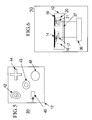
FIG. 1 is a simplified top-down diagram of a die integrated antenna structure in accordance with the present invention.
FIG. 2 is a cross-sectional diagram of the die integrated antenna structure of FIG. 1 shown in accordance with the present invention.
FIG. 3 is a simplified top-down diagram of another die integrated antenna structure in accordance with the present invention.
FIG. 4 is a cross-sectional diagram of the die integrated antenna structure of FIG. 3 shown in accordance with the present invention.
FIG. 5 is a simplified top-down diagram of a die integrated antenna structure showing a variety of antennas in accordance with the present invention.
FIG. 6 is a block diagram of a communication device in accordance with the present invention.
FIG. 7 a flow chart illustrating a method in accordance with the present invention.
Referring to FIGS. 1 and 2, there is shown a simplified top-down diagram and a cross-sectional diagram respectively of a semiconductor die integrated antenna structure 10 having a semiconductor die 12 with a first integrated antenna 14 tuned to a first frequency and coupled to a first circuit 16. The structure 10 further comprises at least a second integrated antenna 18 tuned to a second frequency and coupled to a second circuit 20. Preferably, the first integrated antenna 14 and the second integrated antenna 18 concurrently transmit without creating appreciable interference with each other. The first circuit 16 is preferably a transmitter circuit, a transceiver circuit, or a receiver circuit. Likewise, the second circuit 20 is preferably a transmitter circuit, a transceiver circuit, or a receiver circuit. The plurality of two or more die integrated antennas addresses the needs of ubiquitous wireless communication by providing for a device designed for easy manufacturability and integration with other wireless system components. By using multiple antenna instantiations that are tuned to different frequencies rather than using tuning mechanisms, multiple concurrent transmissions and receptions can occur efficiently with improved performance. Antenna switching design complexity is also further simplified by having each antenna instantiation with independent transmit and/or receive circuitry.
The advantages of using die integrated antenna structures include the ability to achieve low cost wireless enabled semiconductor products that provides frequency diversity without the circuit and manufacturing complexities associated with conventional implementations of such combinations. The die integrated antenna structures further enable simultaneous multi-frequency operation for bandwidth aggregation that a single antenna solution cannot provide.
Referring to FIGS. 3 and 4, there is shown another simplified top-down diagram and a cross-section diagram respectively of a semiconductor die integrated antenna structure 30 having a semiconductor die 12 with a first integrated antenna 14 tuned to a first frequency and coupled to a first circuit 16 and at least a second integrated antenna 18 coupled to a second circuit 20 as previously shown in FIGS. 1 and 2. In addition, structure 30 comprises a modem 17 that forms a part of the first circuit 16 and a second modem 21 that forms a part of the second circuit 20 as shown. In this embodiment, each antenna instantiation has a dedicated modem that is necessary for simultaneous multi-frequency transmissions. Ideally, this is generally suited for multi-protocol digital communications that is easier to engineer and implement. The frequencies of the first and second antennas are selected for the desired operating characteristics of the target designs.
It should be understood that the present invention is not limited to the antenna design pattern shown in FIGS. 1-4, but could comprise many different variations as shown in FIG. 5, where the antenna patterns can be a patch (48), a dipole (44), a monopole, a loop (43), a ¼ wave open-line (46), or a spiral (42) antenna, or other antenna types including, but not limited to crossed antenna types at 90 degrees orientation fed 90 degrees apart to achieve circular polarization for example.
Referring to FIG. 6, a communication device 50 operating at a plurality of frequencies preferably comprises a processor 36 coupled to a semiconductor die integrated antenna structure 30 having a semiconductor die 12, a first integrated antenna 14 tuned to a first frequency and coupled to a first circuit 17 and at least a second integrated antenna 18 tuned to a second frequency and coupled to a second circuit 21. The processor 36 preferably controls either of the first circuit or the second circuit or both. As described above, the first circuit 17 and the second circuit 21 can each be a receiver circuit, a transmitter circuit or a transceiver circuit. The first and/or second circuits can also take the form of a modem. Alternatively, an embedded processor 37 that can be embedded in the semiconductor die 12 can be used instead of (or in addition to) the separate processor 36 to provide the same functions as processor 36. The embodiments shown in FIG. 6 are ideally suited for both process specific radio/antenna embodiments (using an RF optimized Germanium process for example) as well as fully integrated embodiments using CMOS radio technology.
Referring to FIG. 7, a flow chart illustrating a method 100 of transmitting and receiving a plurality of signals at a plurality of antennas in a semiconductor die integrated antenna structure is shown. At step 102 a first integrated antenna in the semiconductor die tuned to a first frequency and coupled to a first transceiver circuit and a first modem is provided. At step 104, at least a second integrated antenna in the semiconductor die tuned to a second frequency and coupled to a second circuit and a second transceiver circuit and a second modem is provided. At step 106 a portion of the plurality of signals at the first frequency is either transmitted or received or both. At step 108, another portion of the plurality of signals at the second frequency is either transmitted or received or both. Optionally, at step 110 the transmissions and receptions occurring at steps 106 and 108 can occur simultaneously. In many instances, having two independent channels increases the overall capacity and efficiency of a communication system utilizing more than one frequency.
The description above is intended by way of example only and is not intended to limit the present invention in any way except as set forth in the following claims.
Claims (20)
1. A semiconductor die integrated antenna structure, comprising:
a first integrated antenna in a semiconductor die tuned to a first frequency and coupled to a first circuit; and
at least a second integrated antenna in the semiconductor die tuned to a second frequency and coupled to a second circuit, wherein the first circuit is independent of the second circuit enabling simultaneous multi-frequency transmissions.
2. The structure of claim 1 , wherein the first integrated antenna and the at least second integrated antenna concurrently transmit without creating appreciable interference to each other.
3. The structure of claim 1 , wherein the first circuit is a transmitter circuit.
4. The structure of claim 1 , wherein the first circuit is a receiver circuit.
5. The structure of claim 1 , wherein the first circuit is a transceiver circuit.
6. The structure of claim 1 , wherein the second circuit is a transmitter circuit.
7. The structure of claim 1 , wherein the second circuit is a receiver circuit.
8. The structure of claim 1 , wherein the second circuit is a transceiver circuit.
9. The structure of claim 1 , wherein the first circuit further comprises a first modem circuit.
10. The structure of claim 1 , wherein the second circuit further comprises a second modem circuit.
11. The structure of claim 1 , wherein the first antenna and at least the second antenna are selected from the group of antennas comprising patch antennas, dipole antennas, monopole antennas, loop antennas, spiral antennas, ¼ wave open-line antennas, crossed antenna types at 90 degrees orientation fed 90 degrees apart to achieve circular polarization, and any combination thereof.
12. A communication device operating at a plurality of frequencies, comprising:
a semiconductor die integrated antenna structure comprising a first integrated antenna in a semiconductor die tuned to a first frequency and coupled to a first circuit and at least a second integrated antenna in the semiconductor die tuned to a second frequency and coupled to a second circuit; and
a processor embedded in the semiconductor die for controlling either of the first circuit or the second circuit.
13. The communication device of claim 12 , wherein the first integrated antenna and the at least second integrated antenna concurrently transmit without creating appreciable interference with each other.
14. The communication device of claim 12 , wherein the first circuit is selected from the group comprising a transmitter circuit, a receiver circuit, or a transceiver circuit.
15. The communication device of claim 12 , wherein the second circuit is selected from the group comprising a transmitter circuit, a receiver circuit, or a transceiver circuit.
16. The communication device of claim 12 , wherein the first circuit further comprises a first modem circuit.
17. The communication device of claim 12 , wherein the second circuit further comprises a second modem circuit.
18. The communication device of claim 12 , wherein the processor is embedded in the semiconductor die.
19. A method of transmitting and receiving a plurality of signals at a plurality of antennas in a semiconductor die integrated antenna structure, comprising the steps of:
providing a first integrated antenna in the semiconductor die tuned to a first frequency and coupled to a first transceiver circuit and a first modem in the semiconductor die;
providing at least a second integrated antenna in the semiconductor die tuned to a second frequency and coupled to a second transceiver circuit and a second modem in the semiconductor die;
transmitting and/or receiving a portion of the plurality of signals at the first frequency; and
transmitting and/or receiving another portion of the plurality of signals at the second frequency.
20. The method of claim 19 , wherein the method further comprises the step of transmitting at the first frequency from the first integrated antenna and transmitting at the second frequency from the second integrated antenna.
Priority Applications (1)
| Application Number | Priority Date | Filing Date | Title |
|---|---|---|---|
| US09/813,561 US6512482B1 (en) | 2001-03-20 | 2001-03-20 | Method and apparatus using a semiconductor die integrated antenna structure |
Applications Claiming Priority (1)
| Application Number | Priority Date | Filing Date | Title |
|---|---|---|---|
| US09/813,561 US6512482B1 (en) | 2001-03-20 | 2001-03-20 | Method and apparatus using a semiconductor die integrated antenna structure |
Publications (1)
| Publication Number | Publication Date |
|---|---|
| US6512482B1 true US6512482B1 (en) | 2003-01-28 |
Family
ID=25212734
Family Applications (1)
| Application Number | Title | Priority Date | Filing Date |
|---|---|---|---|
| US09/813,561 Expired - Lifetime US6512482B1 (en) | 2001-03-20 | 2001-03-20 | Method and apparatus using a semiconductor die integrated antenna structure |
Country Status (1)
| Country | Link |
|---|---|
| US (1) | US6512482B1 (en) |
Cited By (60)
| Publication number | Priority date | Publication date | Assignee | Title |
|---|---|---|---|---|
| US20030184404A1 (en) * | 2002-03-28 | 2003-10-02 | Mike Andrews | Waveguide adapter |
| US20040219895A1 (en) * | 2003-04-30 | 2004-11-04 | O. Kenneth K. | Layout and architecture for reduced noise coupling between circuitry and on-chip antenna |
| US20040232935A1 (en) * | 2003-05-23 | 2004-11-25 | Craig Stewart | Chuck for holding a device under test |
| US20050140386A1 (en) * | 2003-12-24 | 2005-06-30 | Eric Strid | Active wafer probe |
| US20050156610A1 (en) * | 2002-01-25 | 2005-07-21 | Peter Navratil | Probe station |
| US20050179427A1 (en) * | 2000-09-05 | 2005-08-18 | Cascade Microtech, Inc. | Probe station |
| US20050184744A1 (en) * | 1992-06-11 | 2005-08-25 | Cascademicrotech, Inc. | Wafer probe station having a skirting component |
| US20050212044A1 (en) * | 2001-03-19 | 2005-09-29 | Semiconductor Energy Laboratory Co., Ltd. | Inspection method and inspection apparatus |
| US20060017646A1 (en) * | 2004-07-21 | 2006-01-26 | Denso Corporation | Transceiver-integrated antenna |
| US20060043962A1 (en) * | 2004-09-13 | 2006-03-02 | Terry Burcham | Double sided probing structures |
| US20060092505A1 (en) * | 2004-11-02 | 2006-05-04 | Umech Technologies, Co. | Optically enhanced digital imaging system |
| US20060132157A1 (en) * | 1992-06-11 | 2006-06-22 | Cascade Microtech, Inc. | Wafer probe station having environment control enclosure |
| US20060170441A1 (en) * | 2005-01-31 | 2006-08-03 | Cascade Microtech, Inc. | Interface for testing semiconductors |
| US20060169897A1 (en) * | 2005-01-31 | 2006-08-03 | Cascade Microtech, Inc. | Microscope system for testing semiconductors |
| US20060184041A1 (en) * | 2005-01-31 | 2006-08-17 | Cascade Microtech, Inc. | System for testing semiconductors |
| US20060263952A1 (en) * | 2001-03-19 | 2006-11-23 | Semiconductor Energy Laboratory Co., Ltd. | Method of manufacturing a semiconductor device |
| US20060279299A1 (en) * | 2005-06-08 | 2006-12-14 | Cascade Microtech Inc. | High frequency probe |
| US20060290357A1 (en) * | 2005-06-13 | 2006-12-28 | Richard Campbell | Wideband active-passive differential signal probe |
| US20070024423A1 (en) * | 2005-07-28 | 2007-02-01 | Intermec Ip Corp. | Automatic data collection device, method and article |
| US20070075724A1 (en) * | 2004-06-07 | 2007-04-05 | Cascade Microtech, Inc. | Thermal optical chuck |
| US20070075716A1 (en) * | 2002-05-23 | 2007-04-05 | Cascade Microtech, Inc. | Probe for testing a device under test |
| US20070109001A1 (en) * | 1995-04-14 | 2007-05-17 | Cascade Microtech, Inc. | System for evaluating probing networks |
| US20070194803A1 (en) * | 1997-05-28 | 2007-08-23 | Cascade Microtech, Inc. | Probe holder for testing of a test device |
| US20070194778A1 (en) * | 2002-12-13 | 2007-08-23 | Cascade Microtech, Inc. | Guarded tub enclosure |
| US20070200580A1 (en) * | 2000-12-04 | 2007-08-30 | Cascade Microtech, Inc. | Wafer probe |
| US20070205784A1 (en) * | 2003-05-06 | 2007-09-06 | Cascade Microtech, Inc. | Switched suspended conductor and connection |
| US20070229261A1 (en) * | 2006-04-03 | 2007-10-04 | Intermec Ip Corp. | Automatic data collection device, method and article |
| US20070245536A1 (en) * | 1998-07-14 | 2007-10-25 | Cascade Microtech,, Inc. | Membrane probing system |
| US7302663B1 (en) | 2003-12-31 | 2007-11-27 | Xilinx, Inc. | Automatic antenna diode insertion for integrated circuits |
| US20070285112A1 (en) * | 2006-06-12 | 2007-12-13 | Cascade Microtech, Inc. | On-wafer test structures |
| US20080011822A1 (en) * | 2006-07-11 | 2008-01-17 | Intermec Ip Corp. | Automatic data collection device, method and article |
| US20080042671A1 (en) * | 2003-05-23 | 2008-02-21 | Cascade Microtech, Inc. | Probe for testing a device under test |
| US20080042642A1 (en) * | 2000-09-05 | 2008-02-21 | Cascade Microtech, Inc. | Chuck for holding a device under test |
| US20080042673A1 (en) * | 2002-11-13 | 2008-02-21 | Cascade Microtech, Inc. | Probe for combined signals |
| US20080048693A1 (en) * | 1997-06-06 | 2008-02-28 | Cascade Microtech, Inc. | Probe station having multiple enclosures |
| US20080054922A1 (en) * | 2002-11-08 | 2008-03-06 | Cascade Microtech, Inc. | Probe station with low noise characteristics |
| US7355420B2 (en) | 2001-08-21 | 2008-04-08 | Cascade Microtech, Inc. | Membrane probing system |
| US20080106476A1 (en) * | 2006-11-02 | 2008-05-08 | Allen Minh-Triet Tran | Adaptable antenna system |
| US20080157795A1 (en) * | 2004-07-07 | 2008-07-03 | Cascade Microtech, Inc. | Probe head having a membrane suspended probe |
| US20080157796A1 (en) * | 2003-12-24 | 2008-07-03 | Peter Andrews | Chuck with integrated wafer support |
| US20080218187A1 (en) * | 2003-10-22 | 2008-09-11 | Cascade Microtech, Inc. | Probe testing structure |
| US7429926B1 (en) | 2005-07-20 | 2008-09-30 | Xilinx, Inc. | Radio frequency identification (RFID) and programmable logic device (PLD) integration and applications |
| US20080252424A1 (en) * | 2005-09-21 | 2008-10-16 | Intermec Ip Corp. | Stochastic Communication Protocol Method and System For Radio Frequency Identification (Rfid) Tags Based on Coalition Formation, Such as For Tag-To-Tag Communication |
| US20080265038A1 (en) * | 2004-07-23 | 2008-10-30 | Fractus, S.A. | Antenna in Package with Reduced Electromagnetic Interaction with on Chip Elements |
| US20090061796A1 (en) * | 2007-08-27 | 2009-03-05 | Nokia Corporation | Antenna arrangement |
| US20090189623A1 (en) * | 2007-08-08 | 2009-07-30 | Campbell Richard L | Differential waveguide probe |
| US20090224783A1 (en) * | 1996-08-08 | 2009-09-10 | Cascade Microtech, Inc. | Membrane probing system with local contact scrub |
| US20090237306A1 (en) * | 2005-12-02 | 2009-09-24 | University Of Florida Research Foundation, Inc | Compact integrated monopole antennas |
| US20100085069A1 (en) * | 2008-10-06 | 2010-04-08 | Smith Kenneth R | Impedance optimized interface for membrane probe application |
| US7723999B2 (en) | 2006-06-12 | 2010-05-25 | Cascade Microtech, Inc. | Calibration structures for differential signal probing |
| US20100127725A1 (en) * | 2008-11-21 | 2010-05-27 | Smith Kenneth R | Replaceable coupon for a probing apparatus |
| US7750652B2 (en) | 2006-06-12 | 2010-07-06 | Cascade Microtech, Inc. | Test structure and probe for differential signals |
| US7764072B2 (en) | 2006-06-12 | 2010-07-27 | Cascade Microtech, Inc. | Differential signal probing system |
| US20100231461A1 (en) * | 2009-03-13 | 2010-09-16 | Qualcomm Incorporated | Frequency selective multi-band antenna for wireless communication devices |
| US20100328185A1 (en) * | 2002-11-07 | 2010-12-30 | Jordi Soler Castany | Radio-frequency system in package including antenna |
| US8319503B2 (en) | 2008-11-24 | 2012-11-27 | Cascade Microtech, Inc. | Test apparatus for measuring a characteristic of a device under test |
| US10438032B1 (en) | 2017-11-28 | 2019-10-08 | Wells Fargo Bank, N.A. | Data-securing chip card construction |
| US10657535B1 (en) | 2017-12-05 | 2020-05-19 | Wells Fargo Bank, N.A. | Secure card not present transactions using chip-enabled cards |
| US20200160143A1 (en) * | 2015-12-23 | 2020-05-21 | Idemia France | An electronic wireless communication device having two electronic chips and a method of fabricating such a device |
| US10726219B1 (en) | 2017-11-28 | 2020-07-28 | Wells Fargo Bank, N.A. | Data-securing chip card construction |
Citations (7)
| Publication number | Priority date | Publication date | Assignee | Title |
|---|---|---|---|---|
| US5019829A (en) | 1989-02-08 | 1991-05-28 | Heckman Douglas E | Plug-in package for microwave integrated circuit having cover-mounted antenna |
| US5023624A (en) | 1988-10-26 | 1991-06-11 | Harris Corporation | Microwave chip carrier package having cover-mounted antenna element |
| US5142698A (en) | 1988-06-08 | 1992-08-25 | Nec Corporation | Microwave integrated apparatus including antenna pattern for satellite broadcasting receiver |
| US5612513A (en) * | 1995-09-19 | 1997-03-18 | Micron Communications, Inc. | Article and method of manufacturing an enclosed electrical circuit using an encapsulant |
| US6061025A (en) | 1995-12-07 | 2000-05-09 | Atlantic Aerospace Electronics Corporation | Tunable microstrip patch antenna and control system therefor |
| US6326544B1 (en) * | 1996-02-05 | 2001-12-04 | Micron Technology, Inc. | Polymer based circuit |
| US6373447B1 (en) * | 1998-12-28 | 2002-04-16 | Kawasaki Steel Corporation | On-chip antenna, and systems utilizing same |
-
2001
- 2001-03-20 US US09/813,561 patent/US6512482B1/en not_active Expired - Lifetime
Patent Citations (7)
| Publication number | Priority date | Publication date | Assignee | Title |
|---|---|---|---|---|
| US5142698A (en) | 1988-06-08 | 1992-08-25 | Nec Corporation | Microwave integrated apparatus including antenna pattern for satellite broadcasting receiver |
| US5023624A (en) | 1988-10-26 | 1991-06-11 | Harris Corporation | Microwave chip carrier package having cover-mounted antenna element |
| US5019829A (en) | 1989-02-08 | 1991-05-28 | Heckman Douglas E | Plug-in package for microwave integrated circuit having cover-mounted antenna |
| US5612513A (en) * | 1995-09-19 | 1997-03-18 | Micron Communications, Inc. | Article and method of manufacturing an enclosed electrical circuit using an encapsulant |
| US6061025A (en) | 1995-12-07 | 2000-05-09 | Atlantic Aerospace Electronics Corporation | Tunable microstrip patch antenna and control system therefor |
| US6326544B1 (en) * | 1996-02-05 | 2001-12-04 | Micron Technology, Inc. | Polymer based circuit |
| US6373447B1 (en) * | 1998-12-28 | 2002-04-16 | Kawasaki Steel Corporation | On-chip antenna, and systems utilizing same |
Non-Patent Citations (1)
| Title |
|---|
| Mannion, Patrick; "Single-radio point-to-point delivers 311 Mbits/s"; EE Times article published Feb. 20, 2001 at www.eet.com/story/OEG20010220S0085. |
Cited By (140)
| Publication number | Priority date | Publication date | Assignee | Title |
|---|---|---|---|---|
| US20060132157A1 (en) * | 1992-06-11 | 2006-06-22 | Cascade Microtech, Inc. | Wafer probe station having environment control enclosure |
| US20080106290A1 (en) * | 1992-06-11 | 2008-05-08 | Cascade Microtech, Inc. | Wafer probe station having environment control enclosure |
| US20050184744A1 (en) * | 1992-06-11 | 2005-08-25 | Cascademicrotech, Inc. | Wafer probe station having a skirting component |
| US20070109001A1 (en) * | 1995-04-14 | 2007-05-17 | Cascade Microtech, Inc. | System for evaluating probing networks |
| US7893704B2 (en) | 1996-08-08 | 2011-02-22 | Cascade Microtech, Inc. | Membrane probing structure with laterally scrubbing contacts |
| US20090224783A1 (en) * | 1996-08-08 | 2009-09-10 | Cascade Microtech, Inc. | Membrane probing system with local contact scrub |
| US20070194803A1 (en) * | 1997-05-28 | 2007-08-23 | Cascade Microtech, Inc. | Probe holder for testing of a test device |
| US20080048693A1 (en) * | 1997-06-06 | 2008-02-28 | Cascade Microtech, Inc. | Probe station having multiple enclosures |
| US7681312B2 (en) | 1998-07-14 | 2010-03-23 | Cascade Microtech, Inc. | Membrane probing system |
| US7761986B2 (en) | 1998-07-14 | 2010-07-27 | Cascade Microtech, Inc. | Membrane probing method using improved contact |
| US20070283555A1 (en) * | 1998-07-14 | 2007-12-13 | Cascade Microtech, Inc. | Membrane probing system |
| US8451017B2 (en) | 1998-07-14 | 2013-05-28 | Cascade Microtech, Inc. | Membrane probing method using improved contact |
| US20070245536A1 (en) * | 1998-07-14 | 2007-10-25 | Cascade Microtech,, Inc. | Membrane probing system |
| US20080042669A1 (en) * | 2000-09-05 | 2008-02-21 | Cascade Microtech, Inc. | Probe station |
| US20050179427A1 (en) * | 2000-09-05 | 2005-08-18 | Cascade Microtech, Inc. | Probe station |
| US20080054884A1 (en) * | 2000-09-05 | 2008-03-06 | Cascade Microtech, Inc. | Chuck for holding a device under test |
| US20080042674A1 (en) * | 2000-09-05 | 2008-02-21 | John Dunklee | Chuck for holding a device under test |
| US20080042670A1 (en) * | 2000-09-05 | 2008-02-21 | Cascade Microtech, Inc. | Probe station |
| US20080042376A1 (en) * | 2000-09-05 | 2008-02-21 | Cascade Microtech, Inc. | Probe station |
| US7969173B2 (en) | 2000-09-05 | 2011-06-28 | Cascade Microtech, Inc. | Chuck for holding a device under test |
| US20100109695A1 (en) * | 2000-09-05 | 2010-05-06 | Cascade Microtech, Inc. | Chuck for holding a device under test |
| US20080042642A1 (en) * | 2000-09-05 | 2008-02-21 | Cascade Microtech, Inc. | Chuck for holding a device under test |
| US7688062B2 (en) | 2000-09-05 | 2010-03-30 | Cascade Microtech, Inc. | Probe station |
| US7761983B2 (en) | 2000-12-04 | 2010-07-27 | Cascade Microtech, Inc. | Method of assembling a wafer probe |
| US7688097B2 (en) | 2000-12-04 | 2010-03-30 | Cascade Microtech, Inc. | Wafer probe |
| US20070200580A1 (en) * | 2000-12-04 | 2007-08-30 | Cascade Microtech, Inc. | Wafer probe |
| US20090212792A1 (en) * | 2001-03-19 | 2009-08-27 | Semiconductor Energy Laboratory Co., Ltd. | Inspection Method and Inspection Apparatus |
| US20060263952A1 (en) * | 2001-03-19 | 2006-11-23 | Semiconductor Energy Laboratory Co., Ltd. | Method of manufacturing a semiconductor device |
| US7902845B2 (en) | 2001-03-19 | 2011-03-08 | Semiconductor Energy Laboratory Co., Ltd. | Inspection method and inspection apparatus |
| US20110148220A1 (en) * | 2001-03-19 | 2011-06-23 | Semiconductor Energy Laboratory Co., Ltd. | Inspection Method and Inspection Apparatus |
| US20050212044A1 (en) * | 2001-03-19 | 2005-09-29 | Semiconductor Energy Laboratory Co., Ltd. | Inspection method and inspection apparatus |
| US7674635B2 (en) | 2001-03-19 | 2010-03-09 | Semiconductor Energy Laboratory Co., Ltd. | Method of manufacturing a semiconductor device |
| US7532018B2 (en) * | 2001-03-19 | 2009-05-12 | Semiconductor Energy Laboratory Co., Ltd. | Inspection method and inspection apparatus |
| US8664967B2 (en) | 2001-03-19 | 2014-03-04 | Semiconductor Energy Laboratory Co., Ltd. | Inspection method and inspection apparatus |
| US8729548B2 (en) | 2001-03-19 | 2014-05-20 | Semiconductor Energy Laboratory Co., Ltd. | Method of manufacturing a semiconductor device |
| US9047796B2 (en) | 2001-03-19 | 2015-06-02 | Semiconductor Energy Laboratory Co., Ltd. | Method of manufacturing a semiconductor device |
| US7492175B2 (en) | 2001-08-21 | 2009-02-17 | Cascade Microtech, Inc. | Membrane probing system |
| US7355420B2 (en) | 2001-08-21 | 2008-04-08 | Cascade Microtech, Inc. | Membrane probing system |
| US20080042675A1 (en) * | 2002-01-25 | 2008-02-21 | Cascade Microtech, Inc. | Probe station |
| US20050156610A1 (en) * | 2002-01-25 | 2005-07-21 | Peter Navratil | Probe station |
| US20030184404A1 (en) * | 2002-03-28 | 2003-10-02 | Mike Andrews | Waveguide adapter |
| US20070075716A1 (en) * | 2002-05-23 | 2007-04-05 | Cascade Microtech, Inc. | Probe for testing a device under test |
| US20080024149A1 (en) * | 2002-05-23 | 2008-01-31 | Cascade Microtech, Inc. | Probe for testing a device under test |
| US8421686B2 (en) * | 2002-11-07 | 2013-04-16 | Fractus, S.A. | Radio-frequency system in package including antenna |
| US20100328185A1 (en) * | 2002-11-07 | 2010-12-30 | Jordi Soler Castany | Radio-frequency system in package including antenna |
| US10056691B2 (en) | 2002-11-07 | 2018-08-21 | Fractus, S.A. | Integrated circuit package including miniature antenna |
| US9761948B2 (en) | 2002-11-07 | 2017-09-12 | Fractus, S.A. | Integrated circuit package including miniature antenna |
| US9077073B2 (en) | 2002-11-07 | 2015-07-07 | Fractus, S.A. | Integrated circuit package including miniature antenna |
| US10644405B2 (en) | 2002-11-07 | 2020-05-05 | Fractus, S.A. | Integrated circuit package including miniature antenna |
| US10320079B2 (en) | 2002-11-07 | 2019-06-11 | Fractus, S.A. | Integrated circuit package including miniature antenna |
| US20080054922A1 (en) * | 2002-11-08 | 2008-03-06 | Cascade Microtech, Inc. | Probe station with low noise characteristics |
| US20080074129A1 (en) * | 2002-11-13 | 2008-03-27 | Cascade Microtech, Inc. | Probe for combined signals |
| US20080042673A1 (en) * | 2002-11-13 | 2008-02-21 | Cascade Microtech, Inc. | Probe for combined signals |
| US20070194778A1 (en) * | 2002-12-13 | 2007-08-23 | Cascade Microtech, Inc. | Guarded tub enclosure |
| US20040219895A1 (en) * | 2003-04-30 | 2004-11-04 | O. Kenneth K. | Layout and architecture for reduced noise coupling between circuitry and on-chip antenna |
| US7466998B2 (en) | 2003-04-30 | 2008-12-16 | University Of Florida Research Foundation, Inc. | Layout and architecture for reduced noise coupling between circuitry and on-chip antenna |
| US20070205784A1 (en) * | 2003-05-06 | 2007-09-06 | Cascade Microtech, Inc. | Switched suspended conductor and connection |
| US20090267625A1 (en) * | 2003-05-23 | 2009-10-29 | Cascade Microtech, Inc. | Probe for testing a device under test |
| US7876115B2 (en) | 2003-05-23 | 2011-01-25 | Cascade Microtech, Inc. | Chuck for holding a device under test |
| US7898273B2 (en) | 2003-05-23 | 2011-03-01 | Cascade Microtech, Inc. | Probe for testing a device under test |
| US20040232935A1 (en) * | 2003-05-23 | 2004-11-25 | Craig Stewart | Chuck for holding a device under test |
| US7492172B2 (en) | 2003-05-23 | 2009-02-17 | Cascade Microtech, Inc. | Chuck for holding a device under test |
| US20080042671A1 (en) * | 2003-05-23 | 2008-02-21 | Cascade Microtech, Inc. | Probe for testing a device under test |
| US20090153167A1 (en) * | 2003-05-23 | 2009-06-18 | Craig Stewart | Chuck for holding a device under test |
| US8069491B2 (en) | 2003-10-22 | 2011-11-29 | Cascade Microtech, Inc. | Probe testing structure |
| US20080218187A1 (en) * | 2003-10-22 | 2008-09-11 | Cascade Microtech, Inc. | Probe testing structure |
| US20080157796A1 (en) * | 2003-12-24 | 2008-07-03 | Peter Andrews | Chuck with integrated wafer support |
| US20050140386A1 (en) * | 2003-12-24 | 2005-06-30 | Eric Strid | Active wafer probe |
| US20080309358A1 (en) * | 2003-12-24 | 2008-12-18 | Cascade Microtech, Inc. | Active wafer probe |
| US7688091B2 (en) | 2003-12-24 | 2010-03-30 | Cascade Microtech, Inc. | Chuck with integrated wafer support |
| US7759953B2 (en) | 2003-12-24 | 2010-07-20 | Cascade Microtech, Inc. | Active wafer probe |
| US7302663B1 (en) | 2003-12-31 | 2007-11-27 | Xilinx, Inc. | Automatic antenna diode insertion for integrated circuits |
| US20070075724A1 (en) * | 2004-06-07 | 2007-04-05 | Cascade Microtech, Inc. | Thermal optical chuck |
| US20080157795A1 (en) * | 2004-07-07 | 2008-07-03 | Cascade Microtech, Inc. | Probe head having a membrane suspended probe |
| US7372412B2 (en) * | 2004-07-21 | 2008-05-13 | Denso Corporation | Transceiver-integrated antenna |
| US20060017646A1 (en) * | 2004-07-21 | 2006-01-26 | Denso Corporation | Transceiver-integrated antenna |
| US20080265038A1 (en) * | 2004-07-23 | 2008-10-30 | Fractus, S.A. | Antenna in Package with Reduced Electromagnetic Interaction with on Chip Elements |
| US8330259B2 (en) | 2004-07-23 | 2012-12-11 | Fractus, S.A. | Antenna in package with reduced electromagnetic interaction with on chip elements |
| US20080265925A1 (en) * | 2004-09-13 | 2008-10-30 | Cascade Microtech, Inc. | Double sided probing structures |
| US7420381B2 (en) | 2004-09-13 | 2008-09-02 | Cascade Microtech, Inc. | Double sided probing structures |
| US20060043962A1 (en) * | 2004-09-13 | 2006-03-02 | Terry Burcham | Double sided probing structures |
| US8013623B2 (en) | 2004-09-13 | 2011-09-06 | Cascade Microtech, Inc. | Double sided probing structures |
| US20060092505A1 (en) * | 2004-11-02 | 2006-05-04 | Umech Technologies, Co. | Optically enhanced digital imaging system |
| US7656172B2 (en) | 2005-01-31 | 2010-02-02 | Cascade Microtech, Inc. | System for testing semiconductors |
| US7940069B2 (en) | 2005-01-31 | 2011-05-10 | Cascade Microtech, Inc. | System for testing semiconductors |
| US20060170441A1 (en) * | 2005-01-31 | 2006-08-03 | Cascade Microtech, Inc. | Interface for testing semiconductors |
| US7898281B2 (en) | 2005-01-31 | 2011-03-01 | Cascade Mircotech, Inc. | Interface for testing semiconductors |
| US20090134896A1 (en) * | 2005-01-31 | 2009-05-28 | Cascade Microtech, Inc. | Interface for testing semiconductors |
| US20060169897A1 (en) * | 2005-01-31 | 2006-08-03 | Cascade Microtech, Inc. | Microscope system for testing semiconductors |
| US20060184041A1 (en) * | 2005-01-31 | 2006-08-17 | Cascade Microtech, Inc. | System for testing semiconductors |
| US20100097467A1 (en) * | 2005-01-31 | 2010-04-22 | Cascade Microtech, Inc. | System for testing semiconductors |
| US20060279299A1 (en) * | 2005-06-08 | 2006-12-14 | Cascade Microtech Inc. | High frequency probe |
| US20090079451A1 (en) * | 2005-06-08 | 2009-03-26 | Cascade Microtech, Inc. | High frequency probe |
| US20060290357A1 (en) * | 2005-06-13 | 2006-12-28 | Richard Campbell | Wideband active-passive differential signal probe |
| US7429926B1 (en) | 2005-07-20 | 2008-09-30 | Xilinx, Inc. | Radio frequency identification (RFID) and programmable logic device (PLD) integration and applications |
| US20070024423A1 (en) * | 2005-07-28 | 2007-02-01 | Intermec Ip Corp. | Automatic data collection device, method and article |
| US7893813B2 (en) * | 2005-07-28 | 2011-02-22 | Intermec Ip Corp. | Automatic data collection device, method and article |
| US20080252424A1 (en) * | 2005-09-21 | 2008-10-16 | Intermec Ip Corp. | Stochastic Communication Protocol Method and System For Radio Frequency Identification (Rfid) Tags Based on Coalition Formation, Such as For Tag-To-Tag Communication |
| US8199689B2 (en) | 2005-09-21 | 2012-06-12 | Intermec Ip Corp. | Stochastic communication protocol method and system for radio frequency identification (RFID) tags based on coalition formation, such as for tag-to-tag communication |
| US8488510B2 (en) | 2005-09-21 | 2013-07-16 | Intermec Ip Corp. | Stochastic communication protocol method and system for radio frequency identification (RFID) tags based on coalition formation, such as for tag-to-tag communication |
| US20090237306A1 (en) * | 2005-12-02 | 2009-09-24 | University Of Florida Research Foundation, Inc | Compact integrated monopole antennas |
| US20070229261A1 (en) * | 2006-04-03 | 2007-10-04 | Intermec Ip Corp. | Automatic data collection device, method and article |
| US8120461B2 (en) * | 2006-04-03 | 2012-02-21 | Intermec Ip Corp. | Automatic data collection device, method and article |
| US20070285112A1 (en) * | 2006-06-12 | 2007-12-13 | Cascade Microtech, Inc. | On-wafer test structures |
| US7764072B2 (en) | 2006-06-12 | 2010-07-27 | Cascade Microtech, Inc. | Differential signal probing system |
| US7750652B2 (en) | 2006-06-12 | 2010-07-06 | Cascade Microtech, Inc. | Test structure and probe for differential signals |
| US7723999B2 (en) | 2006-06-12 | 2010-05-25 | Cascade Microtech, Inc. | Calibration structures for differential signal probing |
| US20090021273A1 (en) * | 2006-06-12 | 2009-01-22 | Cascade Microtech, Inc. | On-wafer test structures |
| US20080011822A1 (en) * | 2006-07-11 | 2008-01-17 | Intermec Ip Corp. | Automatic data collection device, method and article |
| US8002173B2 (en) | 2006-07-11 | 2011-08-23 | Intermec Ip Corp. | Automatic data collection device, method and article |
| CN101529657B (en) * | 2006-11-02 | 2014-09-03 | 高通股份有限公司 | Adaptable antenna system |
| WO2008055039A3 (en) * | 2006-11-02 | 2008-09-12 | Qualcomm Inc | Adaptable antenna system |
| US20080106476A1 (en) * | 2006-11-02 | 2008-05-08 | Allen Minh-Triet Tran | Adaptable antenna system |
| WO2008055039A2 (en) * | 2006-11-02 | 2008-05-08 | Qualcomm Incorporated | Adaptable antenna system |
| US8781522B2 (en) | 2006-11-02 | 2014-07-15 | Qualcomm Incorporated | Adaptable antenna system |
| US7876114B2 (en) | 2007-08-08 | 2011-01-25 | Cascade Microtech, Inc. | Differential waveguide probe |
| US20090189623A1 (en) * | 2007-08-08 | 2009-07-30 | Campbell Richard L | Differential waveguide probe |
| US20090061796A1 (en) * | 2007-08-27 | 2009-03-05 | Nokia Corporation | Antenna arrangement |
| US8121539B2 (en) * | 2007-08-27 | 2012-02-21 | Nokia Corporation | Antenna arrangement |
| US7888957B2 (en) | 2008-10-06 | 2011-02-15 | Cascade Microtech, Inc. | Probing apparatus with impedance optimized interface |
| US20100085069A1 (en) * | 2008-10-06 | 2010-04-08 | Smith Kenneth R | Impedance optimized interface for membrane probe application |
| US20100127725A1 (en) * | 2008-11-21 | 2010-05-27 | Smith Kenneth R | Replaceable coupon for a probing apparatus |
| US9429638B2 (en) | 2008-11-21 | 2016-08-30 | Cascade Microtech, Inc. | Method of replacing an existing contact of a wafer probing assembly |
| US10267848B2 (en) | 2008-11-21 | 2019-04-23 | Formfactor Beaverton, Inc. | Method of electrically contacting a bond pad of a device under test with a probe |
| US8410806B2 (en) | 2008-11-21 | 2013-04-02 | Cascade Microtech, Inc. | Replaceable coupon for a probing apparatus |
| US8319503B2 (en) | 2008-11-24 | 2012-11-27 | Cascade Microtech, Inc. | Test apparatus for measuring a characteristic of a device under test |
| US20100231461A1 (en) * | 2009-03-13 | 2010-09-16 | Qualcomm Incorporated | Frequency selective multi-band antenna for wireless communication devices |
| US20200160143A1 (en) * | 2015-12-23 | 2020-05-21 | Idemia France | An electronic wireless communication device having two electronic chips and a method of fabricating such a device |
| US10846586B2 (en) * | 2015-12-23 | 2020-11-24 | Idemia France | Electronic wireless communication device having two electronic chips and a method of fabricating such a device |
| US10832021B1 (en) | 2017-11-28 | 2020-11-10 | Wells Fargo Bank, N.A. | Data-securing chip card construction |
| US10726219B1 (en) | 2017-11-28 | 2020-07-28 | Wells Fargo Bank, N.A. | Data-securing chip card construction |
| US10776591B1 (en) | 2017-11-28 | 2020-09-15 | Wells Fargo Bank, N.A. | Data-securing chip card construction |
| US10832022B1 (en) | 2017-11-28 | 2020-11-10 | Wells Fargo Bank, N.A. | Data-securing chip card construction |
| US10438032B1 (en) | 2017-11-28 | 2019-10-08 | Wells Fargo Bank, N.A. | Data-securing chip card construction |
| US11334729B1 (en) | 2017-11-28 | 2022-05-17 | Wells Fargo Bank, N.A. | Data-securing chip card construction |
| US11704511B2 (en) | 2017-11-28 | 2023-07-18 | Wells Fargo Bank, N.A. | Data-securing chip card construction |
| US10657535B1 (en) | 2017-12-05 | 2020-05-19 | Wells Fargo Bank, N.A. | Secure card not present transactions using chip-enabled cards |
| US10891625B1 (en) | 2017-12-05 | 2021-01-12 | Wells Fargo Bank, N.A. | Secure card not present transactions using chip-enabled cards |
| US11436609B1 (en) | 2017-12-05 | 2022-09-06 | Wells Fargo Bank, N.A. | Secure card not present transactions using chip-enabled cards |
| US11790374B1 (en) | 2017-12-05 | 2023-10-17 | Wells Fargo Bank, N.A. | Secure card not present transactions using chip-enabled cards |
Similar Documents
| Publication | Publication Date | Title |
|---|---|---|
| US6512482B1 (en) | Method and apparatus using a semiconductor die integrated antenna structure | |
| US8792848B2 (en) | Programmable wireless communication device | |
| US7764932B2 (en) | Antenna system for use within a wireless communication device | |
| US7729722B2 (en) | Calibration of wireless communication device | |
| US8270925B2 (en) | Extended antenna module and applications thereof | |
| US8200168B2 (en) | Programmable antenna assembly and applications thereof | |
| US7035654B2 (en) | System and method for providing GPS-enabled wireless communications | |
| US8862073B2 (en) | Configurable antenna structure | |
| US20040038660A1 (en) | RF front-end for dual-mode wireless LAN module | |
| TWI249914B (en) | Multiple antenna apparatus and method to provide interference detection and cancellation | |
| JP4425711B2 (en) | Antenna control method and radio transmission / reception apparatus | |
| EP1476961B1 (en) | System and method for providing gps-enabled wireless communications | |
| US6249255B1 (en) | Antenna assembly, and associated method, having parasitic element for altering antenna pattern characteristics | |
| CN104079311A (en) | Communication system and communication control method | |
| US7505435B2 (en) | RF circuitry and compact hybrid for wireless communication devices | |
| JP2000077924A (en) | Transmitter/receiver | |
| TW200843193A (en) | Antenna module and apparatus using the same | |
| Tsakalaki et al. | Spatial spectrum sensing for wireless handheld terminals: design challenges and novel solutions based on tunable parasitic antennas [Dynamic Spectrum Management] | |
| CN101715247B (en) | Multi standby portable terminal | |
| US7542009B2 (en) | Wireless communication device and signal receiving/transmitting method thereof | |
| JP2022092589A (en) | Baluns with integrated matching networks | |
| CN111509405A (en) | Antenna module and electronic equipment | |
| CN216850329U (en) | Antenna structure and intelligent wearable device | |
| JP2004320309A (en) | Multiband wireless device | |
| JP2005072749A (en) | Radio system and communication method using the same |
Legal Events
| Date | Code | Title | Description |
|---|---|---|---|
| AS | Assignment |
Owner name: XILINX, INC., CALIFORNIA Free format text: ASSIGNMENT OF ASSIGNORS INTEREST;ASSIGNORS:NELSON, MICHAEL D.;LESEA, AUSTIN H.;AGATEP, ANTOLIN S.;REEL/FRAME:011681/0402 Effective date: 20010320 |
|
| STCF | Information on status: patent grant |
Free format text: PATENTED CASE |
|
| FPAY | Fee payment |
Year of fee payment: 4 |
|
| FPAY | Fee payment |
Year of fee payment: 8 |
|
| FPAY | Fee payment |
Year of fee payment: 12 |