US6515506B1 - Circuit for reducing pin count of a semiconductor chip and method for configuring the chip - Google Patents
Circuit for reducing pin count of a semiconductor chip and method for configuring the chip Download PDFInfo
- Publication number
- US6515506B1 US6515506B1 US09/564,711 US56471100A US6515506B1 US 6515506 B1 US6515506 B1 US 6515506B1 US 56471100 A US56471100 A US 56471100A US 6515506 B1 US6515506 B1 US 6515506B1
- Authority
- US
- United States
- Prior art keywords
- external
- external input
- configuration data
- communication
- memory
- Prior art date
- Legal status (The legal status is an assumption and is not a legal conclusion. Google has not performed a legal analysis and makes no representation as to the accuracy of the status listed.)
- Expired - Lifetime
Links
Images


Classifications
-
- H—ELECTRICITY
- H03—ELECTRONIC CIRCUITRY
- H03K—PULSE TECHNIQUE
- H03K19/00—Logic circuits, i.e. having at least two inputs acting on one output; Inverting circuits
- H03K19/02—Logic circuits, i.e. having at least two inputs acting on one output; Inverting circuits using specified components
- H03K19/173—Logic circuits, i.e. having at least two inputs acting on one output; Inverting circuits using specified components using elementary logic circuits as components
- H03K19/1731—Optimisation thereof
- H03K19/1732—Optimisation thereof by limitation or reduction of the pin/gate ratio
Definitions
- the present invention relates to a circuit that reduces external terminal or pin count of a semiconductor chip, such as a communications chip or other type of chip that requires the generation of configuration data. More particularly, the invention relates to a circuit that reduces the number of external input terminals or pins required for generating the configuration data. The invention also relates to a method for generating configuration data for a semiconductor chip using a reduced number of external terminals or pins. The invention further relates to an Ethernet or network card in which the chip and circuit may be embodied and to which the configuration data generating method may be applied.
- ICs such as Ethernet chips
- LANs local area networks
- WANs wide area networks
- Intranet networks become more important in day-to-day business activities.
- chips As such chips become more widely used, they are also becoming more highly integrated to perform an increasing number of interface functions. The problem is that an increase in functionality tends to increase chip pin count.
- IC design it is desirable to provide more functions using the same number of pins, or to provide the same functions using fewer pins.
- Using fewer pins has the advantage of reducing the size of the chip and the expense of packaging the chip. For example, a design that uses only six pins to perform a certain function is superior to a design that requires eight pins to perform the same function.
- an integrated circuit comprises a plurality of multiplexers, each of which has a first input in communication with output data and a second input in communication with configuration data; a plurality of external output terminals in communication with an output of a respective one of the plurality of multiplexers; an external input terminal; and a memory in communication with the external input terminal.
- the external input terminal is connectable with a selected one of the plurality of external output terminals.
- the integrated circuit further comprises a signal generator in communication with the second input of each of the plurality of multiplexers.
- the configuration data comprises an n-bit sequence
- the memory comprises an n-bit shift register.
- the integrated circuit further comprises a second external input terminal and a second memory in communication with the second external input terminal, wherein the second external input terminal is connectable with a selected one of the plurality of external output terminals.
- the configuration data may comprise an n-bit sequence and an m-bit sequence
- the first memory comprises an n-bit shift register
- the second memory comprises an m-bit shift register.
- the integrated circuit may be formed on a circuit board which further includes a connector in communication with the external input terminal and selected one of the plurality of external output terminals.
- the circuit board may further include a plurality of light emitting diodes, each in communication with a respective one of the plurality of external output terminals.
- a method for configuring an integrated circuit comprises (a) selecting output data or configuration data to generate a plurality of output streams; (b) outputting from the integrated circuit each of the plurality of output streams; (c) inputting to the integrated circuit one of the plurality of output streams; and (d) storing configuration data input in step (c) when configuration data is selected in step (a).
- the configuration data preferably comprises an n-bit sequence
- the memory means comprises an n-bit shift register.
- a network communications system which includes a computer system that comprises the above-described integrated circuit and a connector in communication with the external input terminal and a selected one of the plurality of external output terminals.
- the system may further include a plurality of light emitting diodes, each in communication with a respective one of the plurality of external output terminals.
- FIG. 1 and FIG. 1 a are functional block diagrams of an integrated circuit, constructed in accordance with aspects of the invention.
- FIG. 2 is a timing diagram illustrating the timing of various signals identified in FIG. 1 .
- FIG. 3 is a flow chart illustrating a process by which configuration data is generated, in accordance with an aspect of the invention.
- FIG. 4 is a functional block diagram of an exemplary network communications chip in which the circuit of FIG. 1 may be embodied.
- FIG. 5 is a functional block diagram illustrating the architecture of an exemplary computer system in which the network communications chip of FIG. 4 may be used.
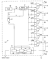
- an integrated circuit 12 illustrates aspects of the invention.
- the circuit 12 may be embodied on a circuit board or semiconductor chip 14 , such as a communications chip, which may be, for example, an Ethernet transceiver for use in 1000BASE-T, 100BASE-TX or 10BASE-T applications. While the present invention has particular utility in connection with an Ethernet communications chip operating in accordance with Ethernet standards and protocols, the invention is not so limited. The invention may also be employed with other communications chips operating according to other network standards and protocols, or with other chips that require the generation of configuration data.
- circuit 12 is designed to reduce the external terminal count of chip 14 by reducing the number of external input terminals needed for generating configuration data, e.g., during initialization of the chip.
- the circuit 12 includes a plurality of multiplexers 15 , 16 , 17 , 18 , 19 and 20 , each having an output in communication with a respective one of a plurality of external output terminals, such as output pins 21 , 22 , 23 , 24 , 25 and 26 on which digital output signals A, B, C, D, E and F are generated.
- Each output signal is representative of a sequence one or more bits in length. In the illustrated embodiment, these sequences each comprise 3 bits.
- output signals A, B, C, D, E and F represent bit sequences 001 , 010 , 011 , 100 , 101 and 110 respectively.
- Bit sequences 000 and 111 are respectively generated from the V SS and V DD connections of the chip. With a 3-bit sequence generated on each output pin, six output pins plus V SS and V DD are used to generate all possible 3-bit combinations. However, different bit sequence lengths will require different numbers of output pins. In general, with V SS and V DD being used to respectively generate the all low and the all high sequences, the number of output pins needed to generate all combinations of an n-bit sequence is 2 n ⁇ 2.
- Each multiplexer has a first input in communication with primary output data of the Ethernet transceiver which may be a light emitting diode (LED) signal.
- primary output data of the Ethernet transceiver which may be a light emitting diode (LED) signal.
- LED 1 through LED 6 there are six primary output data signals, designated LED 1 through LED 6 , one for each multiplexer.
- LED 1 through LED 6 are generated by an on-chip controller (not shown).
- Each multiplexer also has a second input in communication with a configuration data signal J.
- the configuration data signal J is generated by an appropriate signal generator 31 that is controlled by a timing device such as a clock 32 .
- Each of the multiplexers also receives a selection signal S that determines which of the two inputs is selected.
- a selected number of external output terminals or pins are used to generate configuration data through a reduced number of external input terminals or pins.
- an appropriate one of the output pins, V SS or V DD , according to which 3-bit value is desired, is coupled, via a selector 71 , to a single external input terminal, such as input pin 35 , that is in communication with the serial input of a shift register 43 .
- Selector 41 may be a jumper, DIP switch, or equivalent structure.
- the present invention further may comprise a second memory 43 ′ in communication with a second external input terminal 35 ′, such that the second external input terminal 43 ′ is connectable via selector 41 ′ with a selected one of the plurality of external output terminals as shown in FIG. 1 a.
- circuit 12 includes q n-bit shift registers, q input pins, each coupled to the input of a respective one of the q shift registers, and q selectors, one associated with a respective one of the q shift registers.
- each of the q selectors is coupled to an output pin, V SS or V DD to input the desired n-bit configuration code into the corresponding shift register.
- selectors may be coupled to the output pins, V SS and V DD in any number of different combinations, including combinations where more than one selector is coupled to the same output pin.
- each of the q configuration codes may be of different bit lengths, in which case the q shift registers may also be of different sizes.
- the configuration data may comprise an n-bit sequence that is shifted into to a first n-bit shift register and an m-bit sequence that is shifted into a second m-bit shift register.
- Each of the shift registers 43 may be implemented, for example, with a chain of n flip-flops connected in cascade, with the output of one flip-flop connected to the input of the next flip-flop.
- a 3-bit shift register having 3 flip-flops, respectively identified by the reference numerals 44 , 45 and 46 , is shown.
- Each flip-flop stores one bit of information and receives a pulse P from a two-input AND gate 51 that causes that flip-flop to shift its binary information one position to the left.
- the serial input on input pin 35 determines what goes into the rightmost flip-flop, e.g., flip-flop 44 , during the shift, and the contents of the left-most flip-flop, e.g., flip-flop 46 , determines the serial output of the shift register.
- the AND gate 51 controls the shift so that it occurs only with certain clock signals but not with others. Specifically, the serial shift of information occurs only when both the clock signal CL and a shift control signal X, which are inputs to the AND gate, are in the “1” or “high” state.
- Signal X is generated by signal generator 31 in response to an externally generated reset signal R.
- Signal X is synchronized with signals J and S also generated by the signal generator and changes value just after the negative edge of a clock pulse, as shown in the timing diagram of FIG. 2 .
- FIG. 2 also shows the timing of reset signal R, output signals A through F, V SS , V DD , select signal S, and the pulse signal P generated by AND gate 51 .
- FIG. 3 is a flow chart illustrating a process by which configuration data is generated using the output pins and a reduced number of input pins, in accordance with another aspect of the invention.
- each of q selectors 41 is connected between (i) an output pin, V SS or V DD and (ii) a corresponding input pin of a particular shift register.
- a configuration code is then generated on that output pin, V SS or V DD and shifted in to a particular shift register in step 302 . This is done by serially inputting the configuration code on that output pin, V SS or V DD into the particular shift register, as described above.
- the number of input pins on the chip is reduced from q ⁇ n to q, in the case where all of the configuration codes are of the same length. This is a significant reduction when n is large. Such a reduction of input pins has the further advantage of reducing the size of the chip.
- circuit 12 may be embodied on a network communications chip, such as an Ethernet transceiver, which may be, for example, a highly integrated physical layer device for Ethernet applications.
- FIG. 4 is a functional block diagram of such a device 54 in which circuit 12 may be embodied.
- the illustrated chip is manufactured using digital CMOS process and contains all of the active circuitry required to implement the physical layer functions to transmit and receive data on standard CAT5 unshielded twisted pair cable.
- the illustrated chip has an IEEE 802.3 compliant Gigabit Media Independent Interface (GMII) and a 10-bit (TBI) interface that interfaces directly onto a MAC/switch port.
- GMII Gigabit Media Independent Interface
- TBI 10-bit interface
- Speed selection is achieved through the Auto-Negotiation function.
- Mixed-signal processing technology is employed to perform equalization, echo and cross-talk cancellation, data recovery and error correction at a gigabit per second data rate.
- FIG. 4 is adapted to be used in connection with a computer system to enable the computer to link with other computers in a network, such as a LAN.
- FIG. 5 is a functional block diagram illustrating the architecture of an exemplary computer system 60 that may be employed in such a network using the network communications chip.
- the computer system includes bus 61 that interconnects central processing unit (CPU) 62 , system memory 63 and device interfaces.
- Bus 61 can be implemented by more than one physical bus such as a system bus and a processor local bus.
- CPU 62 represents processing circuitry such as a microprocessor, and may also include additional processors such as a floating point processor or a graphics processor.
- System memory 63 may include various memory components, such as random-access memory (RAM) and read-only memory (ROM).
- Input controller 64 represents interface circuitry that connects to one or more input devices 65 such as a keyboard, mouse, track ball and/or stylus.
- Display controller 66 represents interface circuitry that connects to one or more display devices 67 such as a cathode ray tube (CRT) display, liquid crystal display (LCD), or thin film transistor (TFT) display.
- Storage controller 68 represents interface circuitry that connects to one or more external and/or internal storage devices 69 , such as a magnetic disk or tape drive, optical disk drive or solid-state storage device, which may be used to store programs and data.
- computer system 60 further includes a communications controller 70 that represents interface circuitry which is adapted to connect to a communications device 71 , such as a network card in which network communications chip 14 and circuit 12 are embodied.
- a communications device 71 such as a network card in which network communications chip 14 and circuit 12 are embodied.
- the network card enables computer system 60 to link to other computers in the network, while incorporating the features and advantages provided by the invention.
- the present invention provides a circuit that reduces the external terminal count of a communications chip by reducing the number of external input terminals required for generating configuration data during initialization of the chip.
- the external input and output terminals are pins; however, the invention is not so limited. More broadly, the external terminals may be external connections, ball gate arrays, as well as other equivalent structure. The invention is also applicable to other types of chips where generation of configuration data is necessary or desirable.
Abstract
Description
Claims (12)
Priority Applications (3)
| Application Number | Priority Date | Filing Date | Title |
|---|---|---|---|
| US09/564,711 US6515506B1 (en) | 2000-05-03 | 2000-05-03 | Circuit for reducing pin count of a semiconductor chip and method for configuring the chip |
| US10/287,528 US6741097B2 (en) | 2000-05-03 | 2002-11-05 | Circuit for reducing pin count of a semiconductor chip and method for configuring the chip |
| US10/287,527 US6831479B2 (en) | 2000-05-03 | 2002-11-05 | Circuit for reducing pin count of a semiconductor chip and method for configuring the chip |
Applications Claiming Priority (1)
| Application Number | Priority Date | Filing Date | Title |
|---|---|---|---|
| US09/564,711 US6515506B1 (en) | 2000-05-03 | 2000-05-03 | Circuit for reducing pin count of a semiconductor chip and method for configuring the chip |
Related Child Applications (2)
| Application Number | Title | Priority Date | Filing Date |
|---|---|---|---|
| US10/287,528 Division US6741097B2 (en) | 2000-05-03 | 2002-11-05 | Circuit for reducing pin count of a semiconductor chip and method for configuring the chip |
| US10/287,527 Continuation US6831479B2 (en) | 2000-05-03 | 2002-11-05 | Circuit for reducing pin count of a semiconductor chip and method for configuring the chip |
Publications (1)
| Publication Number | Publication Date |
|---|---|
| US6515506B1 true US6515506B1 (en) | 2003-02-04 |
Family
ID=24255570
Family Applications (3)
| Application Number | Title | Priority Date | Filing Date |
|---|---|---|---|
| US09/564,711 Expired - Lifetime US6515506B1 (en) | 2000-05-03 | 2000-05-03 | Circuit for reducing pin count of a semiconductor chip and method for configuring the chip |
| US10/287,528 Expired - Lifetime US6741097B2 (en) | 2000-05-03 | 2002-11-05 | Circuit for reducing pin count of a semiconductor chip and method for configuring the chip |
| US10/287,527 Expired - Lifetime US6831479B2 (en) | 2000-05-03 | 2002-11-05 | Circuit for reducing pin count of a semiconductor chip and method for configuring the chip |
Family Applications After (2)
| Application Number | Title | Priority Date | Filing Date |
|---|---|---|---|
| US10/287,528 Expired - Lifetime US6741097B2 (en) | 2000-05-03 | 2002-11-05 | Circuit for reducing pin count of a semiconductor chip and method for configuring the chip |
| US10/287,527 Expired - Lifetime US6831479B2 (en) | 2000-05-03 | 2002-11-05 | Circuit for reducing pin count of a semiconductor chip and method for configuring the chip |
Country Status (1)
| Country | Link |
|---|---|
| US (3) | US6515506B1 (en) |
Cited By (12)
| Publication number | Priority date | Publication date | Assignee | Title |
|---|---|---|---|---|
| US20030057998A1 (en) * | 2000-05-03 | 2003-03-27 | William Lo | Circuit for reducing pin count of a semiconductor chip and method for configuring the chip |
| US20030084195A1 (en) * | 2001-08-24 | 2003-05-01 | Dove Daniel J. | Reduced pin-count system interface for gigabit ethernet physical layer devices |
| US7253658B1 (en) | 2005-06-14 | 2007-08-07 | Xilinx, Inc. | Integrated circuit providing direct access to multi-directional interconnect lines in a general interconnect structure |
| US7256612B1 (en) | 2005-06-14 | 2007-08-14 | Xilinx, Inc. | Programmable logic block providing carry chain with programmable initialization values |
| US7265576B1 (en) | 2005-06-14 | 2007-09-04 | Xilinx, Inc. | Programmable lookup table with dual input and output terminals in RAM mode |
| US7268587B1 (en) | 2005-06-14 | 2007-09-11 | Xilinx, Inc. | Programmable logic block with carry chains providing lookahead functions of different lengths |
| US7274214B1 (en) * | 2005-06-14 | 2007-09-25 | Xilinx, Inc. | Efficient tile layout for a programmable logic device |
| US7276934B1 (en) | 2005-06-14 | 2007-10-02 | Xilinx, Inc. | Integrated circuit with programmable routing structure including diagonal interconnect lines |
| US7375552B1 (en) | 2005-06-14 | 2008-05-20 | Xilinx, Inc. | Programmable logic block with dedicated and selectable lookup table outputs coupled to general interconnect structure |
| US20090267681A1 (en) * | 2008-04-23 | 2009-10-29 | Infineon Technologies Ag | Integrated Circuit and Method of Configuring an Integrated Circuit |
| US20100007535A1 (en) * | 2008-07-10 | 2010-01-14 | Infineon Technologies Ag | Circuit with Calibration Circuit Portion |
| US7804719B1 (en) | 2005-06-14 | 2010-09-28 | Xilinx, Inc. | Programmable logic block having reduced output delay during RAM write processes when programmed to function in RAM mode |
Families Citing this family (70)
| Publication number | Priority date | Publication date | Assignee | Title |
|---|---|---|---|---|
| US6845444B2 (en) * | 2001-08-23 | 2005-01-18 | Silicon Integrated Systems Corp. | Method and apparatus for reducing strapping devices |
| US20100141466A1 (en) * | 2002-04-05 | 2010-06-10 | Mary Thanhhuong Thi Nguyen | System and method for automatic detection of fiber and copper in data switch systems |
| US7193440B1 (en) | 2004-02-14 | 2007-03-20 | Herman Schmit | Configurable circuits, IC's, and systems |
| US7193432B1 (en) | 2004-02-14 | 2007-03-20 | Herman Schmit | VPA logic circuits |
| US7126381B1 (en) | 2004-02-14 | 2006-10-24 | Herman Schmit | VPA interconnect circuit |
| US7284222B1 (en) | 2004-06-30 | 2007-10-16 | Tabula, Inc. | Method and apparatus for identifying connections between configurable nodes in a configurable integrated circuit |
| US7157933B1 (en) | 2004-02-14 | 2007-01-02 | Herman Schmit | Configurable circuits, IC's, and systems |
| US7109752B1 (en) | 2004-02-14 | 2006-09-19 | Herman Schmit | Configurable circuits, IC's, and systems |
| US7126373B1 (en) | 2004-02-14 | 2006-10-24 | Herman Schmit | Configurable logic circuits with commutative properties |
| US7425841B2 (en) | 2004-02-14 | 2008-09-16 | Tabula Inc. | Configurable circuits, IC's, and systems |
| US7167025B1 (en) | 2004-02-14 | 2007-01-23 | Herman Schmit | Non-sequentially configurable IC |
| JP4489454B2 (en) * | 2004-02-16 | 2010-06-23 | 富士通マイクロエレクトロニクス株式会社 | Semiconductor integrated circuit |
| US7312630B2 (en) | 2004-06-30 | 2007-12-25 | Tabula, Inc. | Configurable integrated circuit with built-in turns |
| US7145361B1 (en) | 2004-06-30 | 2006-12-05 | Andre Rohe | Configurable integrated circuit with different connection schemes |
| US7282950B1 (en) | 2004-11-08 | 2007-10-16 | Tabula, Inc. | Configurable IC's with logic resources with offset connections |
| US7193438B1 (en) * | 2004-06-30 | 2007-03-20 | Andre Rohe | Configurable integrated circuit with offset connection |
| US7408382B2 (en) | 2004-06-30 | 2008-08-05 | Tabula, Inc. | Configurable circuits, IC's, and systems |
| US7449915B2 (en) | 2004-06-30 | 2008-11-11 | Tabula Inc. | VPA logic circuits |
| US7439766B2 (en) | 2004-06-30 | 2008-10-21 | Tabula, Inc. | Configurable logic circuits with commutative properties |
| US8319313B1 (en) | 2004-10-26 | 2012-11-27 | Marvell Israel (M.I.S.L) Ltd. | Circuits, systems, and methods for reducing effects of cross talk in I/O lines and wire bonds |
| US7342415B2 (en) * | 2004-11-08 | 2008-03-11 | Tabula, Inc. | Configurable IC with interconnect circuits that also perform storage operations |
| US7259587B1 (en) | 2004-11-08 | 2007-08-21 | Tabula, Inc. | Configurable IC's with configurable logic resources that have asymetric inputs and/or outputs |
| US7224181B1 (en) | 2004-11-08 | 2007-05-29 | Herman Schmit | Clock distribution in a configurable IC |
| US7276933B1 (en) | 2004-11-08 | 2007-10-02 | Tabula, Inc. | Reconfigurable IC that has sections running at different looperness |
| US7330050B2 (en) | 2004-11-08 | 2008-02-12 | Tabula, Inc. | Storage elements for a configurable IC and method and apparatus for accessing data stored in the storage elements |
| US7268586B1 (en) | 2004-11-08 | 2007-09-11 | Tabula, Inc. | Method and apparatus for accessing stored data in a reconfigurable IC |
| US7242216B1 (en) | 2004-11-08 | 2007-07-10 | Herman Schmit | Embedding memory between tile arrangement of a configurable IC |
| US7301368B2 (en) * | 2005-03-15 | 2007-11-27 | Tabula, Inc. | Embedding memory within tile arrangement of a configurable IC |
| US7317331B2 (en) | 2004-11-08 | 2008-01-08 | Tabula, Inc. | Reconfigurable IC that has sections running at different reconfiguration rates |
| US7917559B2 (en) | 2004-11-08 | 2011-03-29 | Tabula, Inc. | Configurable IC's with configurable logic circuits that perform adder and/or subtractor operations |
| US7295037B2 (en) * | 2004-11-08 | 2007-11-13 | Tabula, Inc. | Configurable IC with routing circuits with offset connections |
| US7743085B2 (en) | 2004-11-08 | 2010-06-22 | Tabula, Inc. | Configurable IC with large carry chains |
| US7496879B2 (en) | 2004-12-01 | 2009-02-24 | Tabula, Inc. | Concurrent optimization of physical design and operational cycle assignment |
| US7428721B2 (en) | 2004-12-01 | 2008-09-23 | Tabula, Inc. | Operational cycle assignment in a configurable IC |
| US7236009B1 (en) | 2004-12-01 | 2007-06-26 | Andre Rohe | Operational time extension |
| US7530033B2 (en) | 2005-03-15 | 2009-05-05 | Tabula, Inc. | Method and apparatus for decomposing functions in a configurable IC |
| US7230869B1 (en) | 2005-03-15 | 2007-06-12 | Jason Redgrave | Method and apparatus for accessing contents of memory cells |
| US7298169B2 (en) | 2005-03-15 | 2007-11-20 | Tabula, Inc | Hybrid logic/interconnect circuit in a configurable IC |
| US7825684B2 (en) | 2005-03-15 | 2010-11-02 | Tabula, Inc. | Variable width management for a memory of a configurable IC |
| US7224182B1 (en) | 2005-03-15 | 2007-05-29 | Brad Hutchings | Hybrid configurable circuit for a configurable IC |
| US7310003B2 (en) | 2005-03-15 | 2007-12-18 | Tabula, Inc. | Configurable IC with interconnect circuits that have select lines driven by user signals |
| US7292063B2 (en) * | 2005-05-02 | 2007-11-06 | Lsi Corporation | Method of interconnect for multi-slot metal-mask programmable relocatable function placed in an I/O region |
| US7456655B1 (en) | 2005-05-16 | 2008-11-25 | Marvell Israel (Misl) Ltd. | System and process for overcoming wire-bond originated cross-talk |
| US7512850B2 (en) | 2005-07-15 | 2009-03-31 | Tabula, Inc. | Checkpointing user design states in a configurable IC |
| US7818361B1 (en) | 2005-11-07 | 2010-10-19 | Tabula, Inc. | Method and apparatus for performing two's complement multiplication |
| US7765249B1 (en) | 2005-11-07 | 2010-07-27 | Tabula, Inc. | Use of hybrid interconnect/logic circuits for multiplication |
| US7372297B1 (en) | 2005-11-07 | 2008-05-13 | Tabula Inc. | Hybrid interconnect/logic circuits enabling efficient replication of a function in several sub-cycles to save logic and routing resources |
| US8463836B1 (en) | 2005-11-07 | 2013-06-11 | Tabula, Inc. | Performing mathematical and logical operations in multiple sub-cycles |
| US7679401B1 (en) | 2005-12-01 | 2010-03-16 | Tabula, Inc. | User registers implemented with routing circuits in a configurable IC |
| US7797497B1 (en) | 2006-03-08 | 2010-09-14 | Tabula, Inc. | System and method for providing more logical memory ports than physical memory ports |
| US7694083B1 (en) | 2006-03-08 | 2010-04-06 | Tabula, Inc. | System and method for providing a virtual memory architecture narrower and deeper than a physical memory architecture |
| US7609085B1 (en) | 2006-03-08 | 2009-10-27 | Tabula, Inc. | Configurable integrated circuit with a 4-to-1 multiplexer |
| US7669097B1 (en) | 2006-03-27 | 2010-02-23 | Tabula, Inc. | Configurable IC with error detection and correction circuitry |
| TWI323564B (en) * | 2006-11-22 | 2010-04-11 | Realtek Semiconductor Corp | Initial configuration device of an integrated circuit and initializing method thereof |
| US7930666B1 (en) | 2006-12-12 | 2011-04-19 | Tabula, Inc. | System and method of providing a memory hierarchy |
| TWI339499B (en) * | 2007-02-06 | 2011-03-21 | Realtek Semiconductor Corp | Configured circuit and method thereof |
| TWI339500B (en) * | 2007-02-06 | 2011-03-21 | Realtek Semiconductor Corp | Configured circuit and method thereof |
| US7525344B2 (en) | 2007-03-20 | 2009-04-28 | Tabula, Inc. | Configurable IC having a routing fabric with storage elements |
| US7535252B1 (en) | 2007-03-22 | 2009-05-19 | Tabula, Inc. | Configurable ICs that conditionally transition through configuration data sets |
| US8248101B2 (en) | 2007-09-06 | 2012-08-21 | Tabula, Inc. | Reading configuration data from internal storage node of configuration storage circuit |
| US8990651B2 (en) | 2007-09-19 | 2015-03-24 | Tabula, Inc. | Integrated circuit (IC) with primary and secondary networks and device containing such an IC |
| US8863067B1 (en) | 2008-02-06 | 2014-10-14 | Tabula, Inc. | Sequential delay analysis by placement engines |
| US20090201821A1 (en) * | 2008-02-11 | 2009-08-13 | Barnette James D | System and method for detecting early link failure in an ethernet network |
| US8166435B2 (en) | 2008-06-26 | 2012-04-24 | Tabula, Inc. | Timing operations in an IC with configurable circuits |
| WO2010016857A1 (en) | 2008-08-04 | 2010-02-11 | Tabula, Inc. | Trigger circuits and event counters for an ic |
| US8912820B2 (en) | 2010-04-02 | 2014-12-16 | Tabula, Inc. | System and method for reducing reconfiguration power |
| US8760193B2 (en) | 2011-07-01 | 2014-06-24 | Tabula, Inc. | Configurable storage elements |
| US9148151B2 (en) | 2011-07-13 | 2015-09-29 | Altera Corporation | Configurable storage elements |
| US9203397B1 (en) | 2011-12-16 | 2015-12-01 | Altera Corporation | Delaying start of user design execution |
| US10277228B1 (en) | 2018-01-17 | 2019-04-30 | Seagate Technology Llc | Configuration pin-strapping |
Citations (5)
| Publication number | Priority date | Publication date | Assignee | Title |
|---|---|---|---|---|
| US5168573A (en) * | 1987-08-31 | 1992-12-01 | Digital Equipment Corporation | Memory device for storing vector registers |
| US5446399A (en) | 1994-11-18 | 1995-08-29 | Varian Associates, Inc. | Method and structure for a fault-free input configuration control mechanism |
| US5990577A (en) * | 1996-11-01 | 1999-11-23 | Allied Telesis K. K. | Hub for local area network with backup power supply system |
| US6020760A (en) | 1997-07-16 | 2000-02-01 | Altera Corporation | I/O buffer circuit with pin multiplexing |
| US6026078A (en) | 1997-02-05 | 2000-02-15 | Nortel Networks Corporation | Apparatus and method for providing multiple network port configurations |
Family Cites Families (5)
| Publication number | Priority date | Publication date | Assignee | Title |
|---|---|---|---|---|
| US5701441A (en) * | 1995-08-18 | 1997-12-23 | Xilinx, Inc. | Computer-implemented method of optimizing a design in a time multiplexed programmable logic device |
| US6057705A (en) * | 1998-05-28 | 2000-05-02 | Microchip Technology Incorporated | Programmable pin designation for semiconductor devices |
| US6262596B1 (en) * | 1999-04-05 | 2001-07-17 | Xilinx, Inc. | Configuration bus interface circuit for FPGAS |
| US6255849B1 (en) * | 2000-02-04 | 2001-07-03 | Xilinx, Inc. | On-chip self-modification for PLDs |
| US6515506B1 (en) * | 2000-05-03 | 2003-02-04 | Marvell International, Ltd. | Circuit for reducing pin count of a semiconductor chip and method for configuring the chip |
-
2000
- 2000-05-03 US US09/564,711 patent/US6515506B1/en not_active Expired - Lifetime
-
2002
- 2002-11-05 US US10/287,528 patent/US6741097B2/en not_active Expired - Lifetime
- 2002-11-05 US US10/287,527 patent/US6831479B2/en not_active Expired - Lifetime
Patent Citations (5)
| Publication number | Priority date | Publication date | Assignee | Title |
|---|---|---|---|---|
| US5168573A (en) * | 1987-08-31 | 1992-12-01 | Digital Equipment Corporation | Memory device for storing vector registers |
| US5446399A (en) | 1994-11-18 | 1995-08-29 | Varian Associates, Inc. | Method and structure for a fault-free input configuration control mechanism |
| US5990577A (en) * | 1996-11-01 | 1999-11-23 | Allied Telesis K. K. | Hub for local area network with backup power supply system |
| US6026078A (en) | 1997-02-05 | 2000-02-15 | Nortel Networks Corporation | Apparatus and method for providing multiple network port configurations |
| US6020760A (en) | 1997-07-16 | 2000-02-01 | Altera Corporation | I/O buffer circuit with pin multiplexing |
Non-Patent Citations (1)
| Title |
|---|
| Part 3: Carrier Sense Multiple Access with Collision Detection (CSMA/CD) Access Method and Physical Layer Specifications, IEEE Std 802.3, 1998 Edition, Sections 14, 24, 25, 35, 36 and Supplement. |
Cited By (18)
| Publication number | Priority date | Publication date | Assignee | Title |
|---|---|---|---|---|
| US6831479B2 (en) * | 2000-05-03 | 2004-12-14 | Marvell International Ltd. | Circuit for reducing pin count of a semiconductor chip and method for configuring the chip |
| US20030071652A1 (en) * | 2000-05-03 | 2003-04-17 | William Lo | Circuit for reducing pin count of a semiconductor chip and method for configuring the chip |
| US20030057998A1 (en) * | 2000-05-03 | 2003-03-27 | William Lo | Circuit for reducing pin count of a semiconductor chip and method for configuring the chip |
| US6741097B2 (en) * | 2000-05-03 | 2004-05-25 | Iarvell International, Ltd. | Circuit for reducing pin count of a semiconductor chip and method for configuring the chip |
| US7466668B2 (en) * | 2001-08-24 | 2008-12-16 | Hewlett-Packard Development Company, L.P. | Reduced pin-count system interface for gigabit ethernet physical layer devices |
| US20030084195A1 (en) * | 2001-08-24 | 2003-05-01 | Dove Daniel J. | Reduced pin-count system interface for gigabit ethernet physical layer devices |
| US7375552B1 (en) | 2005-06-14 | 2008-05-20 | Xilinx, Inc. | Programmable logic block with dedicated and selectable lookup table outputs coupled to general interconnect structure |
| US7265576B1 (en) | 2005-06-14 | 2007-09-04 | Xilinx, Inc. | Programmable lookup table with dual input and output terminals in RAM mode |
| US7268587B1 (en) | 2005-06-14 | 2007-09-11 | Xilinx, Inc. | Programmable logic block with carry chains providing lookahead functions of different lengths |
| US7274214B1 (en) * | 2005-06-14 | 2007-09-25 | Xilinx, Inc. | Efficient tile layout for a programmable logic device |
| US7276934B1 (en) | 2005-06-14 | 2007-10-02 | Xilinx, Inc. | Integrated circuit with programmable routing structure including diagonal interconnect lines |
| US7253658B1 (en) | 2005-06-14 | 2007-08-07 | Xilinx, Inc. | Integrated circuit providing direct access to multi-directional interconnect lines in a general interconnect structure |
| US7256612B1 (en) | 2005-06-14 | 2007-08-14 | Xilinx, Inc. | Programmable logic block providing carry chain with programmable initialization values |
| US7804719B1 (en) | 2005-06-14 | 2010-09-28 | Xilinx, Inc. | Programmable logic block having reduced output delay during RAM write processes when programmed to function in RAM mode |
| US20090267681A1 (en) * | 2008-04-23 | 2009-10-29 | Infineon Technologies Ag | Integrated Circuit and Method of Configuring an Integrated Circuit |
| US7816907B2 (en) | 2008-04-23 | 2010-10-19 | Lantiq Deutschland Gmbh | Integrated circuit with a measuring circuit and method of configuring an integrated circuit with a measuring circuit |
| US20100007535A1 (en) * | 2008-07-10 | 2010-01-14 | Infineon Technologies Ag | Circuit with Calibration Circuit Portion |
| US7830285B2 (en) | 2008-07-10 | 2010-11-09 | Lantiq Deutschland Gmbh | Circuit with calibration circuit portion |
Also Published As
| Publication number | Publication date |
|---|---|
| US20030057998A1 (en) | 2003-03-27 |
| US6741097B2 (en) | 2004-05-25 |
| US6831479B2 (en) | 2004-12-14 |
| US20030071652A1 (en) | 2003-04-17 |
Similar Documents
| Publication | Publication Date | Title |
|---|---|---|
| US6515506B1 (en) | Circuit for reducing pin count of a semiconductor chip and method for configuring the chip | |
| EP1670199B1 (en) | Design of channel alignment, error handling, and clock routing using hard-wired blocks for data transmission within programmable logic integrated circuits | |
| US11693810B2 (en) | Interface bridge between integrated circuit die | |
| US7339502B2 (en) | Method and device for transmitting data over a plurality of transmission lines | |
| US5305317A (en) | Local area network adaptive circuit for multiple network types | |
| US6834318B2 (en) | Bidirectional bus repeater for communications on a chip | |
| US7890680B2 (en) | Physical layer device having a serdes pass through mode | |
| US8094668B1 (en) | Physical layer device including a serial media independent interface (SMII) | |
| US20100232485A1 (en) | Single conductor bidirectional communication link | |
| US20030217347A1 (en) | Method and apparatus for optimizing distributed multiplexed bus interconnects | |
| JP3384838B2 (en) | Interface device | |
| US20050099965A1 (en) | Method for computing speed map for IEEE-1394 network | |
| Wu et al. | A flexible FPGA-to-FPGA communication system | |
| JP2000353035A (en) | Signal communication interface formed by integrating single-end type and differential type | |
| US9594715B2 (en) | Integrated circuit devices, systems and methods having automatic configurable mapping of input and/or output data connections | |
| CN117056249A (en) | MDIO-to-AHB conversion method, system, equipment and medium | |
| US6980563B2 (en) | Method and system for fast ethernet serial port multiplexing to reduce I/O pin count | |
| US20040225862A1 (en) | Method and apparatus for interconnecting portions of circuitry within a data processing system | |
| US20030235203A1 (en) | Extender sublayer device | |
| US20240118983A1 (en) | Method for facilitating testing for an interconnection protocol, a controller, and an electronic device | |
| US6697385B1 (en) | Circuit(s), method(s) and architecture for configurable packet re-timing in network repeater hubs | |
| JP2003188929A (en) | Semiconductor integrated circuit and data transfer system | |
| US6954086B2 (en) | Low power data storage element with enhanced noise margin | |
| CN116340254A (en) | Processor system, starting method and computing device | |
| CN114512089A (en) | Display control circuit, display control method, display module and display device |
Legal Events
| Date | Code | Title | Description |
|---|---|---|---|
| AS | Assignment |
Owner name: MARVELL SEMICONDUCTOR, INC., CALIFORNIA Free format text: ASSIGNMENT OF ASSIGNORS INTEREST;ASSIGNOR:LO, WILLIAM;REEL/FRAME:010783/0352 Effective date: 20000502 |
|
| AS | Assignment |
Owner name: MARVELL INTERNATIONAL LTD., BERMUDA Free format text: ASSIGNMENT OF ASSIGNORS INTEREST;ASSIGNOR:MARVELL TECHNOLOGY GROUP, LTD.;REEL/FRAME:011514/0519 Effective date: 20010119 |
|
| STCF | Information on status: patent grant |
Free format text: PATENTED CASE |
|
| FPAY | Fee payment |
Year of fee payment: 4 |
|
| FPAY | Fee payment |
Year of fee payment: 8 |
|
| FPAY | Fee payment |
Year of fee payment: 12 |
|
| AS | Assignment |
Owner name: MARVELL TECHNOLOGY GROUP, LTD., BERMUDA Free format text: ASSIGNMENT OF ASSIGNORS INTEREST;ASSIGNOR:MARVELL SEMICONDUCTOR, INC.;REEL/FRAME:051242/0938 Effective date: 20000502 |
|
| AS | Assignment |
Owner name: CAVIUM INTERNATIONAL, CAYMAN ISLANDS Free format text: ASSIGNMENT OF ASSIGNORS INTEREST;ASSIGNOR:MARVELL INTERNATIONAL LTD.;REEL/FRAME:052918/0001 Effective date: 20191231 |
|
| AS | Assignment |
Owner name: MARVELL ASIA PTE, LTD., SINGAPORE Free format text: ASSIGNMENT OF ASSIGNORS INTEREST;ASSIGNOR:CAVIUM INTERNATIONAL;REEL/FRAME:053475/0001 Effective date: 20191231 |