US6541129B1 - Organic electroluminescence device and phenylenediamine derivative - Google Patents
Organic electroluminescence device and phenylenediamine derivative Download PDFInfo
- Publication number
- US6541129B1 US6541129B1 US09/530,597 US53059700A US6541129B1 US 6541129 B1 US6541129 B1 US 6541129B1 US 53059700 A US53059700 A US 53059700A US 6541129 B1 US6541129 B1 US 6541129B1
- Authority
- US
- United States
- Prior art keywords
- group
- carbon atoms
- substituted
- light emitting
- organic
- Prior art date
- Legal status (The legal status is an assumption and is not a legal conclusion. Google has not performed a legal analysis and makes no representation as to the accuracy of the status listed.)
- Expired - Lifetime
Links
- 150000004986 phenylenediamines Chemical class 0.000 title claims abstract description 38
- 238000005401 electroluminescence Methods 0.000 title claims abstract description 8
- 125000004432 carbon atom Chemical group C* 0.000 claims description 86
- 125000003118 aryl group Chemical group 0.000 claims description 45
- 229910052799 carbon Inorganic materials 0.000 claims description 32
- 125000003545 alkoxy group Chemical group 0.000 claims description 27
- 125000000217 alkyl group Chemical group 0.000 claims description 27
- 125000006615 aromatic heterocyclic group Chemical group 0.000 claims description 22
- 125000005504 styryl group Chemical group 0.000 claims description 21
- 229920006395 saturated elastomer Polymers 0.000 claims description 20
- 125000004435 hydrogen atom Chemical group [H]* 0.000 claims description 17
- 239000000126 substance Substances 0.000 claims description 17
- 125000000732 arylene group Chemical group 0.000 claims description 16
- 125000001624 naphthyl group Chemical group 0.000 claims description 16
- 125000002947 alkylene group Chemical group 0.000 claims description 13
- RTZKZFJDLAIYFH-UHFFFAOYSA-N ether Substances CCOCC RTZKZFJDLAIYFH-UHFFFAOYSA-N 0.000 claims description 12
- 125000005647 linker group Chemical group 0.000 claims description 12
- XMGMFRIEKMMMSU-UHFFFAOYSA-N phenylmethylbenzene Chemical group C=1C=CC=CC=1[C]C1=CC=CC=C1 XMGMFRIEKMMMSU-UHFFFAOYSA-N 0.000 claims description 12
- 229920002554 vinyl polymer Polymers 0.000 claims description 9
- 125000005427 anthranyl group Chemical group 0.000 claims description 8
- 125000001725 pyrenyl group Chemical group 0.000 claims description 7
- 125000000391 vinyl group Chemical group [H]C([*])=C([H])[H] 0.000 claims description 6
- 238000002347 injection Methods 0.000 abstract description 79
- 239000007924 injection Substances 0.000 abstract description 79
- 239000000463 material Substances 0.000 abstract description 52
- 230000001747 exhibiting effect Effects 0.000 abstract description 5
- 239000010410 layer Substances 0.000 description 120
- 150000001875 compounds Chemical class 0.000 description 73
- YXFVVABEGXRONW-UHFFFAOYSA-N Toluene Chemical compound CC1=CC=CC=C1 YXFVVABEGXRONW-UHFFFAOYSA-N 0.000 description 57
- -1 aromatic amine compound Chemical class 0.000 description 43
- 238000000034 method Methods 0.000 description 38
- 238000007740 vapor deposition Methods 0.000 description 36
- 239000002904 solvent Substances 0.000 description 34
- LQNUZADURLCDLV-UHFFFAOYSA-N nitrobenzene Chemical compound [O-][N+](=O)C1=CC=CC=C1 LQNUZADURLCDLV-UHFFFAOYSA-N 0.000 description 28
- BWHMMNNQKKPAPP-UHFFFAOYSA-L potassium carbonate Chemical compound [K+].[K+].[O-]C([O-])=O BWHMMNNQKKPAPP-UHFFFAOYSA-L 0.000 description 28
- VLKZOEOYAKHREP-UHFFFAOYSA-N n-Hexane Chemical compound CCCCCC VLKZOEOYAKHREP-UHFFFAOYSA-N 0.000 description 21
- 238000006243 chemical reaction Methods 0.000 description 17
- 239000010408 film Substances 0.000 description 17
- VYPSYNLAJGMNEJ-UHFFFAOYSA-N silicon dioxide Inorganic materials O=[Si]=O VYPSYNLAJGMNEJ-UHFFFAOYSA-N 0.000 description 17
- 239000013078 crystal Substances 0.000 description 16
- 239000007788 liquid Substances 0.000 description 16
- 239000000741 silica gel Substances 0.000 description 16
- 229910002027 silica gel Inorganic materials 0.000 description 16
- RYGMFSIKBFXOCR-UHFFFAOYSA-N Copper Chemical compound [Cu] RYGMFSIKBFXOCR-UHFFFAOYSA-N 0.000 description 14
- YTPLMLYBLZKORZ-UHFFFAOYSA-N Thiophene Chemical compound C=1C=CSC=1 YTPLMLYBLZKORZ-UHFFFAOYSA-N 0.000 description 14
- 230000015572 biosynthetic process Effects 0.000 description 14
- 229910000027 potassium carbonate Inorganic materials 0.000 description 14
- 238000003756 stirring Methods 0.000 description 14
- 0 CN(C)C1=CC=C(N(C)C2=CC=C(*C3=CC=C(N(C)C4=CC=C(N(C)[Ar])C=C4)C=C3)C=C2)C=C1.[1*]C.[2*]C.[Ar] Chemical compound CN(C)C1=CC=C(N(C)C2=CC=C(*C3=CC=C(N(C)C4=CC=C(N(C)[Ar])C=C4)C=C3)C=C2)C=C1.[1*]C.[2*]C.[Ar] 0.000 description 12
- 238000003786 synthesis reaction Methods 0.000 description 12
- YLQBMQCUIZJEEH-UHFFFAOYSA-N Furan Chemical compound C=1C=COC=1 YLQBMQCUIZJEEH-UHFFFAOYSA-N 0.000 description 10
- KAESVJOAVNADME-UHFFFAOYSA-N Pyrrole Chemical compound C=1C=CNC=1 KAESVJOAVNADME-UHFFFAOYSA-N 0.000 description 10
- SMWDFEZZVXVKRB-UHFFFAOYSA-N Quinoline Chemical compound N1=CC=CC2=CC=CC=C21 SMWDFEZZVXVKRB-UHFFFAOYSA-N 0.000 description 10
- XSCHRSMBECNVNS-UHFFFAOYSA-N quinoxaline Chemical compound N1=CC=NC2=CC=CC=C21 XSCHRSMBECNVNS-UHFFFAOYSA-N 0.000 description 10
- 239000000758 substrate Substances 0.000 description 10
- QTBSBXVTEAMEQO-UHFFFAOYSA-N Acetic acid Chemical compound CC(O)=O QTBSBXVTEAMEQO-UHFFFAOYSA-N 0.000 description 9
- 230000000052 comparative effect Effects 0.000 description 9
- 125000001997 phenyl group Chemical group [H]C1=C([H])C([H])=C(*)C([H])=C1[H] 0.000 description 9
- 239000010409 thin film Substances 0.000 description 9
- 238000000859 sublimation Methods 0.000 description 8
- 230000008022 sublimation Effects 0.000 description 8
- XSOBMWMSZLDXPQ-UHFFFAOYSA-N CC1=CC=C(N(C2=CC=CC=C2)C2=CC=C(N(C3=CC=C(C4=CC=C(N(C5=CC=C(N(C6=CC=CC=C6)C6=CC=C(C)C=C6)C=C5)C5=C6C=CC=CC6=CC=C5)C=C4)C=C3)C3=CC=CC4=C3C=CC=C4)C=C2)C=C1.CC1=CC=C(N(C2=CC=CC=C2)C2=CC=C(N(C3=CC=C(C4=CC=C(N(C5=CC=C(N(C6=CC=CC=C6)C6=CC=C(C)C=C6)C=C5)C5=C6C=CC=CC6=CC=C5)C=C4)C=C3)C3=CC=CC4=C3C=CC=C4)C=C2)C=C1.CC1=CC=C(N(C2=CC=CC=C2)C2=CC=C(N(C3=CC=C(C4=CC=C(N(C5=CC=C(N(C6=CC=CC=C6)C6=CC=C(C)C=C6)C=C5)C5=C6C=CC=CC6=CC=C5)C=C4)C=C3)C3=CC=CC4=C3C=CC=C4)C=C2)C=C1.CC1=CC=C(N(C2=CC=CC=C2)C2=CC=C(N(C3=CC=C(C4=CC=C(N(C5=CC=C(N(C6=CC=CC=C6)C6=CC=C(C)C=C6)C=C5)C5=C6C=CC=CC6=CC=C5)C=C4)C=C3)C3=CC=CC4=C3C=CC=C4)C=C2)C=C1 Chemical compound CC1=CC=C(N(C2=CC=CC=C2)C2=CC=C(N(C3=CC=C(C4=CC=C(N(C5=CC=C(N(C6=CC=CC=C6)C6=CC=C(C)C=C6)C=C5)C5=C6C=CC=CC6=CC=C5)C=C4)C=C3)C3=CC=CC4=C3C=CC=C4)C=C2)C=C1.CC1=CC=C(N(C2=CC=CC=C2)C2=CC=C(N(C3=CC=C(C4=CC=C(N(C5=CC=C(N(C6=CC=CC=C6)C6=CC=C(C)C=C6)C=C5)C5=C6C=CC=CC6=CC=C5)C=C4)C=C3)C3=CC=CC4=C3C=CC=C4)C=C2)C=C1.CC1=CC=C(N(C2=CC=CC=C2)C2=CC=C(N(C3=CC=C(C4=CC=C(N(C5=CC=C(N(C6=CC=CC=C6)C6=CC=C(C)C=C6)C=C5)C5=C6C=CC=CC6=CC=C5)C=C4)C=C3)C3=CC=CC4=C3C=CC=C4)C=C2)C=C1.CC1=CC=C(N(C2=CC=CC=C2)C2=CC=C(N(C3=CC=C(C4=CC=C(N(C5=CC=C(N(C6=CC=CC=C6)C6=CC=C(C)C=C6)C=C5)C5=C6C=CC=CC6=CC=C5)C=C4)C=C3)C3=CC=CC4=C3C=CC=C4)C=C2)C=C1 XSOBMWMSZLDXPQ-UHFFFAOYSA-N 0.000 description 7
- 238000000434 field desorption mass spectrometry Methods 0.000 description 7
- 239000011521 glass Substances 0.000 description 7
- 239000012535 impurity Substances 0.000 description 7
- 239000000843 powder Substances 0.000 description 7
- MCJGNVYPOGVAJF-UHFFFAOYSA-N quinolin-8-ol Chemical class C1=CN=C2C(O)=CC=CC2=C1 MCJGNVYPOGVAJF-UHFFFAOYSA-N 0.000 description 7
- 229930192474 thiophene Natural products 0.000 description 7
- XLYOFNOQVPJJNP-UHFFFAOYSA-N water Chemical compound O XLYOFNOQVPJJNP-UHFFFAOYSA-N 0.000 description 7
- OSQXTXTYKAEHQV-WXUKJITCSA-N 4-methyl-n-[4-[(e)-2-[4-[4-[(e)-2-[4-(4-methyl-n-(4-methylphenyl)anilino)phenyl]ethenyl]phenyl]phenyl]ethenyl]phenyl]-n-(4-methylphenyl)aniline Chemical compound C1=CC(C)=CC=C1N(C=1C=CC(\C=C\C=2C=CC(=CC=2)C=2C=CC(\C=C\C=3C=CC(=CC=3)N(C=3C=CC(C)=CC=3)C=3C=CC(C)=CC=3)=CC=2)=CC=1)C1=CC=C(C)C=C1 OSQXTXTYKAEHQV-WXUKJITCSA-N 0.000 description 6
- KDLHZDBZIXYQEI-UHFFFAOYSA-N Palladium Chemical compound [Pd] KDLHZDBZIXYQEI-UHFFFAOYSA-N 0.000 description 6
- 230000005684 electric field Effects 0.000 description 6
- 238000000746 purification Methods 0.000 description 6
- 238000004528 spin coating Methods 0.000 description 6
- 150000003852 triazoles Chemical class 0.000 description 6
- JYEUMXHLPRZUAT-UHFFFAOYSA-N 1,2,3-triazine Chemical compound C1=CN=NN=C1 JYEUMXHLPRZUAT-UHFFFAOYSA-N 0.000 description 5
- OWWVTWHBNAWUJO-UHFFFAOYSA-N 4-iodo-n,n-diphenylaniline Chemical compound C1=CC(I)=CC=C1N(C=1C=CC=CC=1)C1=CC=CC=C1 OWWVTWHBNAWUJO-UHFFFAOYSA-N 0.000 description 5
- WHXSMMKQMYFTQS-UHFFFAOYSA-N Lithium Chemical compound [Li] WHXSMMKQMYFTQS-UHFFFAOYSA-N 0.000 description 5
- ZCQWOFVYLHDMMC-UHFFFAOYSA-N Oxazole Chemical compound C1=COC=N1 ZCQWOFVYLHDMMC-UHFFFAOYSA-N 0.000 description 5
- CZPWVGJYEJSRLH-UHFFFAOYSA-N Pyrimidine Chemical compound C1=CN=CN=C1 CZPWVGJYEJSRLH-UHFFFAOYSA-N 0.000 description 5
- XAGFODPZIPBFFR-UHFFFAOYSA-N aluminium Chemical group [Al] XAGFODPZIPBFFR-UHFFFAOYSA-N 0.000 description 5
- 230000000694 effects Effects 0.000 description 5
- 125000001449 isopropyl group Chemical group [H]C([H])([H])C([H])(*)C([H])([H])[H] 0.000 description 5
- 229910052744 lithium Inorganic materials 0.000 description 5
- WCPAKWJPBJAGKN-UHFFFAOYSA-N oxadiazole Chemical compound C1=CON=N1 WCPAKWJPBJAGKN-UHFFFAOYSA-N 0.000 description 5
- 125000000843 phenylene group Chemical group C1(=C(C=CC=C1)*)* 0.000 description 5
- 239000004065 semiconductor Substances 0.000 description 5
- 238000001228 spectrum Methods 0.000 description 5
- 238000004544 sputter deposition Methods 0.000 description 5
- 125000000999 tert-butyl group Chemical group [H]C([H])([H])C(*)(C([H])([H])[H])C([H])([H])[H] 0.000 description 5
- GEYOCULIXLDCMW-UHFFFAOYSA-N 1,2-phenylenediamine Chemical group NC1=CC=CC=C1N GEYOCULIXLDCMW-UHFFFAOYSA-N 0.000 description 4
- NHPPIJMARIVBGU-UHFFFAOYSA-N 1-iodonaphthalene Chemical compound C1=CC=C2C(I)=CC=CC2=C1 NHPPIJMARIVBGU-UHFFFAOYSA-N 0.000 description 4
- LFQSCWFLJHTTHZ-UHFFFAOYSA-N Ethanol Chemical compound CCO LFQSCWFLJHTTHZ-UHFFFAOYSA-N 0.000 description 4
- 229910052782 aluminium Inorganic materials 0.000 description 4
- 150000004982 aromatic amines Chemical class 0.000 description 4
- DMBHHRLKUKUOEG-UHFFFAOYSA-N diphenylamine Chemical compound C=1C=CC=CC=1NC1=CC=CC=C1 DMBHHRLKUKUOEG-UHFFFAOYSA-N 0.000 description 4
- 238000001914 filtration Methods 0.000 description 4
- 239000007850 fluorescent dye Substances 0.000 description 4
- 229910052751 metal Inorganic materials 0.000 description 4
- 239000002184 metal Substances 0.000 description 4
- 238000002156 mixing Methods 0.000 description 4
- 150000004866 oxadiazoles Chemical class 0.000 description 4
- 229960003540 oxyquinoline Drugs 0.000 description 4
- UHXOHPVVEHBKKT-UHFFFAOYSA-N 1-(2,2-diphenylethenyl)-4-[4-(2,2-diphenylethenyl)phenyl]benzene Chemical group C=1C=C(C=2C=CC(C=C(C=3C=CC=CC=3)C=3C=CC=CC=3)=CC=2)C=CC=1C=C(C=1C=CC=CC=1)C1=CC=CC=C1 UHXOHPVVEHBKKT-UHFFFAOYSA-N 0.000 description 3
- YEDVRRNLTGKJSW-UHFFFAOYSA-N 1-(4-iodophenyl)-4-nitrobenzene Chemical group C1=CC([N+](=O)[O-])=CC=C1C1=CC=C(I)C=C1 YEDVRRNLTGKJSW-UHFFFAOYSA-N 0.000 description 3
- 239000005725 8-Hydroxyquinoline Substances 0.000 description 3
- UFHFLCQGNIYNRP-UHFFFAOYSA-N Hydrogen Chemical compound [H][H] UFHFLCQGNIYNRP-UHFFFAOYSA-N 0.000 description 3
- FYYHWMGAXLPEAU-UHFFFAOYSA-N Magnesium Chemical compound [Mg] FYYHWMGAXLPEAU-UHFFFAOYSA-N 0.000 description 3
- OKKJLVBELUTLKV-UHFFFAOYSA-N Methanol Chemical compound OC OKKJLVBELUTLKV-UHFFFAOYSA-N 0.000 description 3
- XQVWYOYUZDUNRW-UHFFFAOYSA-N N-Phenyl-1-naphthylamine Chemical compound C=1C=CC2=CC=CC=C2C=1NC1=CC=CC=C1 XQVWYOYUZDUNRW-UHFFFAOYSA-N 0.000 description 3
- 125000006267 biphenyl group Chemical group 0.000 description 3
- 125000002529 biphenylenyl group Chemical group C1(=CC=CC=2C3=CC=CC=C3C12)* 0.000 description 3
- 238000005266 casting Methods 0.000 description 3
- 239000003054 catalyst Substances 0.000 description 3
- 239000000412 dendrimer Substances 0.000 description 3
- 229920000736 dendritic polymer Polymers 0.000 description 3
- 239000000706 filtrate Substances 0.000 description 3
- 125000003983 fluorenyl group Chemical class C1(=CC=CC=2C3=CC=CC=C3CC12)* 0.000 description 3
- 229910052739 hydrogen Inorganic materials 0.000 description 3
- 239000001257 hydrogen Substances 0.000 description 3
- AMGQUBHHOARCQH-UHFFFAOYSA-N indium;oxotin Chemical compound [In].[Sn]=O AMGQUBHHOARCQH-UHFFFAOYSA-N 0.000 description 3
- 239000003446 ligand Substances 0.000 description 3
- 229910052749 magnesium Inorganic materials 0.000 description 3
- 239000011777 magnesium Substances 0.000 description 3
- 238000004519 manufacturing process Methods 0.000 description 3
- NIHNNTQXNPWCJQ-UHFFFAOYSA-N o-biphenylenemethane Natural products C1=CC=C2CC3=CC=CC=C3C2=C1 NIHNNTQXNPWCJQ-UHFFFAOYSA-N 0.000 description 3
- 125000005561 phenanthryl group Chemical group 0.000 description 3
- NLKNQRATVPKPDG-UHFFFAOYSA-M potassium iodide Chemical compound [K+].[I-] NLKNQRATVPKPDG-UHFFFAOYSA-M 0.000 description 3
- 125000005548 pyrenylene group Chemical group 0.000 description 3
- 229910052709 silver Inorganic materials 0.000 description 3
- 239000004332 silver Substances 0.000 description 3
- 239000000243 solution Substances 0.000 description 3
- 125000001424 substituent group Chemical group 0.000 description 3
- QAOWNCQODCNURD-UHFFFAOYSA-N sulfuric acid Substances OS(O)(=O)=O QAOWNCQODCNURD-UHFFFAOYSA-N 0.000 description 3
- 238000002834 transmittance Methods 0.000 description 3
- UWRZIZXBOLBCON-VOTSOKGWSA-N (e)-2-phenylethenamine Chemical class N\C=C\C1=CC=CC=C1 UWRZIZXBOLBCON-VOTSOKGWSA-N 0.000 description 2
- YJTKZCDBKVTVBY-UHFFFAOYSA-N 1,3-Diphenylbenzene Chemical group C1=CC=CC=C1C1=CC=CC(C=2C=CC=CC=2)=C1 YJTKZCDBKVTVBY-UHFFFAOYSA-N 0.000 description 2
- WFQDTOYDVUWQMS-UHFFFAOYSA-N 1-fluoro-4-nitrobenzene Chemical compound [O-][N+](=O)C1=CC=C(F)C=C1 WFQDTOYDVUWQMS-UHFFFAOYSA-N 0.000 description 2
- CSCPPACGZOOCGX-UHFFFAOYSA-N Acetone Chemical compound CC(C)=O CSCPPACGZOOCGX-UHFFFAOYSA-N 0.000 description 2
- 229910001148 Al-Li alloy Inorganic materials 0.000 description 2
- MHKKAXHLAFELPV-UHFFFAOYSA-N C.C1=CC=C(N(C2=CC=CC=C2)C2=CC=C(N(C3=CC=C(C4=CC=C(N(C5=CC=C(N(C6=CC=CC=C6)C6=CC=CC=C6)C=C5)C5=C6C=CC=CC6=CC=C5)C=C4)C=C3)C3=CC=CC4=C3C=CC=C4)C=C2)C=C1 Chemical compound C.C1=CC=C(N(C2=CC=CC=C2)C2=CC=C(N(C3=CC=C(C4=CC=C(N(C5=CC=C(N(C6=CC=CC=C6)C6=CC=CC=C6)C=C5)C5=C6C=CC=CC6=CC=C5)C=C4)C=C3)C3=CC=CC4=C3C=CC=C4)C=C2)C=C1 MHKKAXHLAFELPV-UHFFFAOYSA-N 0.000 description 2
- YVSWIDPWEWNHJN-UHFFFAOYSA-N C1=CC=C(C2=CC=C(N(C3=CC=C(N(C4=CC=CC=C4)C4=CC=CC=C4)C=C3)C3=CC=C(N(C4=CC=CC=C4)C4=CC=CC=C4)C=C3)C=C2)C=C1 Chemical compound C1=CC=C(C2=CC=C(N(C3=CC=C(N(C4=CC=CC=C4)C4=CC=CC=C4)C=C3)C3=CC=C(N(C4=CC=CC=C4)C4=CC=CC=C4)C=C3)C=C2)C=C1 YVSWIDPWEWNHJN-UHFFFAOYSA-N 0.000 description 2
- MJERKSSLYWJHJU-UHFFFAOYSA-N C1=CC=C(N(C2=CC=CC=C2)C2=CC=C(N(C3=CC=C(C4=C5C=CC=CC5=C(C5=CC=C(N(C6=CC=C(N(C7=CC=CC=C7)C7=CC=CC=C7)C=C6)C6=C7C=CC=CC7=CC=C6)C=C5)C5=C4C=CC=C5)C=C3)C3=CC=CC4=C3C=CC=C4)C=C2)C=C1.C1=CC=C(N(C2=CC=CC=C2)C2=CC=C(N(C3=CC=C(C4=CC=C(C5=CC=C(N(C6=CC=C(N(C7=CC=CC=C7)C7=CC=CC=C7)C=C6)C6=C7C=CC=CC7=CC=C6)C=C5)C=C4)C=C3)C3=CC=CC4=C3C=CC=C4)C=C2)C=C1.C1=CC=C(N(C2=CC=CC=C2)C2=CC=C(N(C3=CC=C(OC4=CC=C(N(C5=CC=C(N(C6=CC=CC=C6)C6=CC=CC=C6)C=C5)C5=C6C=CC=CC6=CC=C5)C=C4)C=C3)C3=CC=CC4=C3C=CC=C4)C=C2)C=C1.[H]C([H])(C1=CC=C(N(C2=CC=C(N(C3=CC=CC=C3)C3=CC=CC=C3)C=C2)C2=CC=CC3=C2C=CC=C3)C=C1)C1=CC=C(N(C2=CC=C(N(C3=CC=CC=C3)C3=CC=CC=C3)C=C2)C2=C3C=CC=CC3=CC=C2)C=C1 Chemical compound C1=CC=C(N(C2=CC=CC=C2)C2=CC=C(N(C3=CC=C(C4=C5C=CC=CC5=C(C5=CC=C(N(C6=CC=C(N(C7=CC=CC=C7)C7=CC=CC=C7)C=C6)C6=C7C=CC=CC7=CC=C6)C=C5)C5=C4C=CC=C5)C=C3)C3=CC=CC4=C3C=CC=C4)C=C2)C=C1.C1=CC=C(N(C2=CC=CC=C2)C2=CC=C(N(C3=CC=C(C4=CC=C(C5=CC=C(N(C6=CC=C(N(C7=CC=CC=C7)C7=CC=CC=C7)C=C6)C6=C7C=CC=CC7=CC=C6)C=C5)C=C4)C=C3)C3=CC=CC4=C3C=CC=C4)C=C2)C=C1.C1=CC=C(N(C2=CC=CC=C2)C2=CC=C(N(C3=CC=C(OC4=CC=C(N(C5=CC=C(N(C6=CC=CC=C6)C6=CC=CC=C6)C=C5)C5=C6C=CC=CC6=CC=C5)C=C4)C=C3)C3=CC=CC4=C3C=CC=C4)C=C2)C=C1.[H]C([H])(C1=CC=C(N(C2=CC=C(N(C3=CC=CC=C3)C3=CC=CC=C3)C=C2)C2=CC=CC3=C2C=CC=C3)C=C1)C1=CC=C(N(C2=CC=C(N(C3=CC=CC=C3)C3=CC=CC=C3)C=C2)C2=C3C=CC=CC3=CC=C2)C=C1 MJERKSSLYWJHJU-UHFFFAOYSA-N 0.000 description 2
- GFWAHHSCHZZZOA-UHFFFAOYSA-N CC1=CC=C(N(C2=CC=CC=C2)C2=CC=C(N(C3=CC=C(C4=CC=C(N(C5=CC=C(N(C6=CC=CC=C6)C6=CC=C(C)C=C6)C=C5)C5=C6C=CC=CC6=CC=C5)C=C4)C=C3)C3=CC=CC4=C3C=CC=C4)C=C2)C=C1.CC1=CC=C(N(C2=CC=CC=C2)C2=CC=C(N(C3=CC=C(C4=CC=C(N(C5=CC=C(N(C6=CC=CC=C6)C6=CC=C(C)C=C6)C=C5)C5=C6C=CC=CC6=CC=C5)C=C4)C=C3)C3=CC=CC4=C3C=CC=C4)C=C2)C=C1.CC1=CC=C(N(C2=CC=CC=C2)C2=CC=C(N(C3=CC=C(C4=CC=C(N(C5=CC=C(N(C6=CC=CC=C6)C6=CC=C(C)C=C6)C=C5)C5=C6C=CC=CC6=CC=C5)C=C4)C=C3)C3=CC=CC4=C3C=CC=C4)C=C2)C=C1.CC1=CC=CC=C1N(C1=CC=CC=C1)C1=CC=C(N(C2=CC=C(C3=CC=C(N(C4=CC=C(N(C5=CC=CC=C5)C5=C(C)C=CC=C5)C=C4)C4=C5C=CC=CC5=CC=C4)C=C3)C=C2)C2=CC=CC3=C2C=CC=C3)C=C1 Chemical compound CC1=CC=C(N(C2=CC=CC=C2)C2=CC=C(N(C3=CC=C(C4=CC=C(N(C5=CC=C(N(C6=CC=CC=C6)C6=CC=C(C)C=C6)C=C5)C5=C6C=CC=CC6=CC=C5)C=C4)C=C3)C3=CC=CC4=C3C=CC=C4)C=C2)C=C1.CC1=CC=C(N(C2=CC=CC=C2)C2=CC=C(N(C3=CC=C(C4=CC=C(N(C5=CC=C(N(C6=CC=CC=C6)C6=CC=C(C)C=C6)C=C5)C5=C6C=CC=CC6=CC=C5)C=C4)C=C3)C3=CC=CC4=C3C=CC=C4)C=C2)C=C1.CC1=CC=C(N(C2=CC=CC=C2)C2=CC=C(N(C3=CC=C(C4=CC=C(N(C5=CC=C(N(C6=CC=CC=C6)C6=CC=C(C)C=C6)C=C5)C5=C6C=CC=CC6=CC=C5)C=C4)C=C3)C3=CC=CC4=C3C=CC=C4)C=C2)C=C1.CC1=CC=CC=C1N(C1=CC=CC=C1)C1=CC=C(N(C2=CC=C(C3=CC=C(N(C4=CC=C(N(C5=CC=CC=C5)C5=C(C)C=CC=C5)C=C4)C4=C5C=CC=CC5=CC=C4)C=C3)C=C2)C2=CC=CC3=C2C=CC=C3)C=C1 GFWAHHSCHZZZOA-UHFFFAOYSA-N 0.000 description 2
- 108010043121 Green Fluorescent Proteins Proteins 0.000 description 2
- JFBZPFYRPYOZCQ-UHFFFAOYSA-N [Li].[Al] Chemical compound [Li].[Al] JFBZPFYRPYOZCQ-UHFFFAOYSA-N 0.000 description 2
- 229910045601 alloy Inorganic materials 0.000 description 2
- 239000000956 alloy Substances 0.000 description 2
- REDXJYDRNCIFBQ-UHFFFAOYSA-N aluminium(3+) Chemical compound [Al+3] REDXJYDRNCIFBQ-UHFFFAOYSA-N 0.000 description 2
- 239000005388 borosilicate glass Substances 0.000 description 2
- 239000013522 chelant Substances 0.000 description 2
- 239000011248 coating agent Substances 0.000 description 2
- 238000000576 coating method Methods 0.000 description 2
- 238000001816 cooling Methods 0.000 description 2
- 125000004980 cyclopropylene group Chemical group 0.000 description 2
- 230000003247 decreasing effect Effects 0.000 description 2
- ZUOUZKKEUPVFJK-UHFFFAOYSA-N diphenyl Chemical compound C1=CC=CC=C1C1=CC=CC=C1 ZUOUZKKEUPVFJK-UHFFFAOYSA-N 0.000 description 2
- 239000002019 doping agent Substances 0.000 description 2
- 239000007772 electrode material Substances 0.000 description 2
- 125000001495 ethyl group Chemical group [H]C([H])([H])C([H])([H])* 0.000 description 2
- 239000006081 fluorescent whitening agent Substances 0.000 description 2
- 239000001989 lithium alloy Substances 0.000 description 2
- VNWKTOKETHGBQD-UHFFFAOYSA-N methane Chemical compound C VNWKTOKETHGBQD-UHFFFAOYSA-N 0.000 description 2
- 125000002496 methyl group Chemical group [H]C([H])([H])* 0.000 description 2
- 125000001570 methylene group Chemical group [H]C([H])([*:1])[*:2] 0.000 description 2
- 239000000203 mixture Substances 0.000 description 2
- QYOZRFPMXCWCFQ-UHFFFAOYSA-N n-[2-[10-[2-(naphthalen-1-ylamino)phenyl]anthracen-9-yl]phenyl]naphthalen-1-amine Chemical compound C1=CC=C2C(NC=3C(=CC=CC=3)C=3C4=CC=CC=C4C(C=4C(=CC=CC=4)NC=4C5=CC=CC=C5C=CC=4)=C4C=CC=CC4=3)=CC=CC2=C1 QYOZRFPMXCWCFQ-UHFFFAOYSA-N 0.000 description 2
- 125000004108 n-butyl group Chemical group [H]C([H])([H])C([H])([H])C([H])([H])C([H])([H])* 0.000 description 2
- 125000001280 n-hexyl group Chemical group C(CCCCC)* 0.000 description 2
- 125000000740 n-pentyl group Chemical group [H]C([H])([H])C([H])([H])C([H])([H])C([H])([H])C([H])([H])* 0.000 description 2
- 125000004123 n-propyl group Chemical group [H]C([H])([H])C([H])([H])C([H])([H])* 0.000 description 2
- 230000003647 oxidation Effects 0.000 description 2
- 238000007254 oxidation reaction Methods 0.000 description 2
- 125000002080 perylenyl group Chemical group C1(=CC=C2C=CC=C3C4=CC=CC5=CC=CC(C1=C23)=C45)* 0.000 description 2
- 229920000642 polymer Polymers 0.000 description 2
- 230000002035 prolonged effect Effects 0.000 description 2
- 125000004805 propylene group Chemical group [H]C([H])([H])C([H])([*:1])C([H])([H])[*:2] 0.000 description 2
- 238000005215 recombination Methods 0.000 description 2
- 230000006798 recombination Effects 0.000 description 2
- 125000002914 sec-butyl group Chemical group [H]C([H])([H])C([H])([H])C([H])(*)C([H])([H])[H] 0.000 description 2
- LPXPTNMVRIOKMN-UHFFFAOYSA-M sodium nitrite Chemical compound [Na+].[O-]N=O LPXPTNMVRIOKMN-UHFFFAOYSA-M 0.000 description 2
- 125000006836 terphenylene group Chemical group 0.000 description 2
- XOLBLPGZBRYERU-UHFFFAOYSA-N tin dioxide Chemical compound O=[Sn]=O XOLBLPGZBRYERU-UHFFFAOYSA-N 0.000 description 2
- ODHXBMXNKOYIBV-UHFFFAOYSA-N triphenylamine Chemical compound C1=CC=CC=C1N(C=1C=CC=CC=1)C1=CC=CC=C1 ODHXBMXNKOYIBV-UHFFFAOYSA-N 0.000 description 2
- BCMCBBGGLRIHSE-UHFFFAOYSA-N 1,3-benzoxazole Chemical class C1=CC=C2OC=NC2=C1 BCMCBBGGLRIHSE-UHFFFAOYSA-N 0.000 description 1
- KLCLIOISYBHYDZ-UHFFFAOYSA-N 1,4,4-triphenylbuta-1,3-dienylbenzene Chemical compound C=1C=CC=CC=1C(C=1C=CC=CC=1)=CC=C(C=1C=CC=CC=1)C1=CC=CC=C1 KLCLIOISYBHYDZ-UHFFFAOYSA-N 0.000 description 1
- OMCUOJTVNIHQTI-UHFFFAOYSA-N 1,4-bis(4-phenylphenyl)benzene Chemical group C1=CC=CC=C1C1=CC=C(C=2C=CC(=CC=2)C=2C=CC(=CC=2)C=2C=CC=CC=2)C=C1 OMCUOJTVNIHQTI-UHFFFAOYSA-N 0.000 description 1
- VERMWGQSKPXSPZ-BUHFOSPRSA-N 1-[(e)-2-phenylethenyl]anthracene Chemical class C=1C=CC2=CC3=CC=CC=C3C=C2C=1\C=C\C1=CC=CC=C1 VERMWGQSKPXSPZ-BUHFOSPRSA-N 0.000 description 1
- KJCVRFUGPWSIIH-UHFFFAOYSA-N 1-naphthol Chemical compound C1=CC=C2C(O)=CC=CC2=C1 KJCVRFUGPWSIIH-UHFFFAOYSA-N 0.000 description 1
- KEHISZDJCIBJEK-UHFFFAOYSA-N 1-phenylanthracene-9,10-diamine Chemical compound C1=CC=C2C(N)=C3C=CC=CC3=C(N)C2=C1C1=CC=CC=C1 KEHISZDJCIBJEK-UHFFFAOYSA-N 0.000 description 1
- XFYQEBBUVNLYBR-UHFFFAOYSA-N 12-phthaloperinone Chemical compound C1=CC(N2C(=O)C=3C(=CC=CC=3)C2=N2)=C3C2=CC=CC3=C1 XFYQEBBUVNLYBR-UHFFFAOYSA-N 0.000 description 1
- HYZJCKYKOHLVJF-UHFFFAOYSA-N 1H-benzimidazole Chemical class C1=CC=C2NC=NC2=C1 HYZJCKYKOHLVJF-UHFFFAOYSA-N 0.000 description 1
- SULWTXOWAFVWOY-PHEQNACWSA-N 2,3-bis[(E)-2-phenylethenyl]pyrazine Chemical class C=1C=CC=CC=1/C=C/C1=NC=CN=C1\C=C\C1=CC=CC=C1 SULWTXOWAFVWOY-PHEQNACWSA-N 0.000 description 1
- ZPSJGADGUYYRKE-UHFFFAOYSA-N 2H-pyran-2-one Chemical class O=C1C=CC=CO1 ZPSJGADGUYYRKE-UHFFFAOYSA-N 0.000 description 1
- YBRVSVVVWCFQMG-UHFFFAOYSA-N 4,4'-diaminodiphenylmethane Chemical compound C1=CC(N)=CC=C1CC1=CC=C(N)C=C1 YBRVSVVVWCFQMG-UHFFFAOYSA-N 0.000 description 1
- FDRNXKXKFNHNCA-UHFFFAOYSA-N 4-(4-anilinophenyl)-n-phenylaniline Chemical compound C=1C=C(C=2C=CC(NC=3C=CC=CC=3)=CC=2)C=CC=1NC1=CC=CC=C1 FDRNXKXKFNHNCA-UHFFFAOYSA-N 0.000 description 1
- HLBLWEWZXPIGSM-UHFFFAOYSA-N 4-Aminophenyl ether Chemical compound C1=CC(N)=CC=C1OC1=CC=C(N)C=C1 HLBLWEWZXPIGSM-UHFFFAOYSA-N 0.000 description 1
- ZCYVEMRRCGMTRW-UHFFFAOYSA-N 7553-56-2 Chemical compound [I] ZCYVEMRRCGMTRW-UHFFFAOYSA-N 0.000 description 1
- 150000004325 8-hydroxyquinolines Chemical class 0.000 description 1
- 229910001316 Ag alloy Inorganic materials 0.000 description 1
- WLRYFDIKCKGMHB-UHFFFAOYSA-N C1=CC(C2=CC3=C(C=C2)CCCC3)=CC=C1C1=CC=C(C2=CC3=C(C=C2)CCCC3)C=C1.C1=CC=C(C2=CC3=C(C=C2)C2=C(C=C(C4=CC=CC=C4)C=C2)CC3)C=C1.C1=CC=C(C2=CC=C(C3=CC=C(C4=CC=C(C5=CC=C(C6=CC=CC=C6)C=C5)C=C4)C=C3)C=C2)C=C1.C1=CC=C(C2=CC=C(C3=CC=C(C4=CC=CC=C4)C=C3)C=C2)C=C1.C1=CC=C(C2=CC=C3C(=C2)CC2=CC(C4=CC=CC=C4)=CC=C23)C=C1.C1=CC=C2C(=C1)CC1=CC(C3=CC=C4C(=C3)CC3=CC=CC=C34)=CC=C12.CC1=CC(C)=CC(C2=CC=C(C3=CC=C(C4=CC=C(C5=CC=C(C6=CC(C)=CC(C)=C6)C=C5)C=C4)C=C3)C=C2)=C1.CC1=CC=C(C2=CC=C(C3=CC=C(C4=CC=C(C)C=C4)C=C3)C=C2)C=C1.CC1=CC=C(C2=CC=C(C3=CC=C(C4=CC=C(C)C=C4)C=C34CC3=C(C=CC=C3)C3=C4C=C(C4=CC=C5C(=C4)CCC4=CC=CC=C45)C=C3)C=C2)C=C1.CC1=CC=C(C2=CC=C(C3=CC=C(C4=CC=C(C5=CC=CC=C5)C=C4)C=C3)C=C2)C=C1 Chemical compound C1=CC(C2=CC3=C(C=C2)CCCC3)=CC=C1C1=CC=C(C2=CC3=C(C=C2)CCCC3)C=C1.C1=CC=C(C2=CC3=C(C=C2)C2=C(C=C(C4=CC=CC=C4)C=C2)CC3)C=C1.C1=CC=C(C2=CC=C(C3=CC=C(C4=CC=C(C5=CC=C(C6=CC=CC=C6)C=C5)C=C4)C=C3)C=C2)C=C1.C1=CC=C(C2=CC=C(C3=CC=C(C4=CC=CC=C4)C=C3)C=C2)C=C1.C1=CC=C(C2=CC=C3C(=C2)CC2=CC(C4=CC=CC=C4)=CC=C23)C=C1.C1=CC=C2C(=C1)CC1=CC(C3=CC=C4C(=C3)CC3=CC=CC=C34)=CC=C12.CC1=CC(C)=CC(C2=CC=C(C3=CC=C(C4=CC=C(C5=CC=C(C6=CC(C)=CC(C)=C6)C=C5)C=C4)C=C3)C=C2)=C1.CC1=CC=C(C2=CC=C(C3=CC=C(C4=CC=C(C)C=C4)C=C3)C=C2)C=C1.CC1=CC=C(C2=CC=C(C3=CC=C(C4=CC=C(C)C=C4)C=C34CC3=C(C=CC=C3)C3=C4C=C(C4=CC=C5C(=C4)CCC4=CC=CC=C45)C=C3)C=C2)C=C1.CC1=CC=C(C2=CC=C(C3=CC=C(C4=CC=C(C5=CC=CC=C5)C=C4)C=C3)C=C2)C=C1 WLRYFDIKCKGMHB-UHFFFAOYSA-N 0.000 description 1
- FFWMTKYVIHAHRT-VFUADWLWSA-N C1=CC=C(/C(C2=CC=C(N(C3=CC=CC=C3)C3=CC=C(N(C4=CC=CC=C4)C4=CC=CC=C4)C=C3)C=C2)=C(/C2=CC=CC=C2)C2=CC=C(N(C3=CC=CC=C3)C3=CC=C(N(C4=CC=CC=C4)C4=CC=CC=C4)C=C3)C=C2)C=C1 Chemical compound C1=CC=C(/C(C2=CC=C(N(C3=CC=CC=C3)C3=CC=C(N(C4=CC=CC=C4)C4=CC=CC=C4)C=C3)C=C2)=C(/C2=CC=CC=C2)C2=CC=C(N(C3=CC=CC=C3)C3=CC=C(N(C4=CC=CC=C4)C4=CC=CC=C4)C=C3)C=C2)C=C1 FFWMTKYVIHAHRT-VFUADWLWSA-N 0.000 description 1
- ZRPKJPDSZYCHIT-VWLIMKGVSA-N C1=CC=C(/C(C2=CC=C(N(C3=CC=CC=C3)C3=CC=C(N(C4=CC=CC=C4)C4=CC=CC=C4)C=C3)C=C2)=C(/C2=CC=CC=C2)C2=CC=C(N(C3=CC=CC=C3)C3=CC=C(N(C4=CC=CC=C4)C4=CC=CC=C4)C=C3)C=C2)C=C1.C1=CC=C(N(C2=CC=C(/C=C/C3=CC=C(N(C4=CC=CC=C4)C4=CC=C(N(C5=CC=CC=C5)C5=CC=CC6=C5C=CC=C6)C=C4)C=C3)C=C2)C2=CC=C(N(C3=CC=CC=C3)C3=CC=CC4=C3C=CC=C4)C=C2)C=C1.C1=CC=C(N(C2=CC=CC=C2)C2=CC=C(N(C3=CC=CC=C3)C3=CC=C(/C=C/C4=CC=C(N(C5=CC=CC=C5)C5=CC=C(N(C6=CC=CC=C6)C6=CC=CC=C6)C=C5)C=C4)C=C3)C=C2)C=C1 Chemical compound C1=CC=C(/C(C2=CC=C(N(C3=CC=CC=C3)C3=CC=C(N(C4=CC=CC=C4)C4=CC=CC=C4)C=C3)C=C2)=C(/C2=CC=CC=C2)C2=CC=C(N(C3=CC=CC=C3)C3=CC=C(N(C4=CC=CC=C4)C4=CC=CC=C4)C=C3)C=C2)C=C1.C1=CC=C(N(C2=CC=C(/C=C/C3=CC=C(N(C4=CC=CC=C4)C4=CC=C(N(C5=CC=CC=C5)C5=CC=CC6=C5C=CC=C6)C=C4)C=C3)C=C2)C2=CC=C(N(C3=CC=CC=C3)C3=CC=CC4=C3C=CC=C4)C=C2)C=C1.C1=CC=C(N(C2=CC=CC=C2)C2=CC=C(N(C3=CC=CC=C3)C3=CC=C(/C=C/C4=CC=C(N(C5=CC=CC=C5)C5=CC=C(N(C6=CC=CC=C6)C6=CC=CC=C6)C=C5)C=C4)C=C3)C=C2)C=C1 ZRPKJPDSZYCHIT-VWLIMKGVSA-N 0.000 description 1
- FMTYLOOZPGYKKN-UHFFFAOYSA-N C1=CC=C(C(=CC2=CC=C(C3=CC=C(C4=CC=C(C=C(C5=CC=CC=C5)C5=CC=CC=C5)C=C4)C=C3)C=C2)C2=CC=CC=C2)C=C1.C1=CC=C(N(C2=CC=CC=C2)C2=CC=C(C=CC3=CC=C(C4=CC=C(C=CC5=CC=C(N(C6=CC=CC=C6)C6=CC=CC=C6)C=C5)C=C4)C=C3)C=C2)C=C1 Chemical compound C1=CC=C(C(=CC2=CC=C(C3=CC=C(C4=CC=C(C=C(C5=CC=CC=C5)C5=CC=CC=C5)C=C4)C=C3)C=C2)C2=CC=CC=C2)C=C1.C1=CC=C(N(C2=CC=CC=C2)C2=CC=C(C=CC3=CC=C(C4=CC=C(C=CC5=CC=C(N(C6=CC=CC=C6)C6=CC=CC=C6)C=C5)C=C4)C=C3)C=C2)C=C1 FMTYLOOZPGYKKN-UHFFFAOYSA-N 0.000 description 1
- ISYZGTMBYXSMJR-UHFFFAOYSA-N C1=CC=C(C(=CC2=CC=C(C3=CC=C(N(C4=CC=C(N(C5=CC=CC=C5)C5=CC=CC=C5)C=C4)C4=CC=C(N(C5=CC=CC=C5)C5=CC=CC=C5)C=C4)C=C3)C3=C2C=CC=C3)C2=CC=CC=C2)C=C1.C1=CC=C(C(=CC2=CC=C(C3=CC=C(N(C4=CC=C(N(C5=CC=CC=C5)C5=CC=CC=C5)C=C4)C4=CC=C(N(C5=CC=CC=C5)C5=CC=CC=C5)C=C4)C=C3)C=C2)C2=CC=CC=C2)C=C1.C1=CC=C(C2=CC=C(C(=CC3=CC=C(C4=CC=C(N(C5=CC=C(N(C6=CC=CC=C6)C6=CC=CC=C6)C=C5)C5=CC=C(N(C6=CC=CC=C6)C6=CC=CC=C6)C=C5)C=C4)C=C3)C3=CC=CC=C3)C=C2)C=C1 Chemical compound C1=CC=C(C(=CC2=CC=C(C3=CC=C(N(C4=CC=C(N(C5=CC=CC=C5)C5=CC=CC=C5)C=C4)C4=CC=C(N(C5=CC=CC=C5)C5=CC=CC=C5)C=C4)C=C3)C3=C2C=CC=C3)C2=CC=CC=C2)C=C1.C1=CC=C(C(=CC2=CC=C(C3=CC=C(N(C4=CC=C(N(C5=CC=CC=C5)C5=CC=CC=C5)C=C4)C4=CC=C(N(C5=CC=CC=C5)C5=CC=CC=C5)C=C4)C=C3)C=C2)C2=CC=CC=C2)C=C1.C1=CC=C(C2=CC=C(C(=CC3=CC=C(C4=CC=C(N(C5=CC=C(N(C6=CC=CC=C6)C6=CC=CC=C6)C=C5)C5=CC=C(N(C6=CC=CC=C6)C6=CC=CC=C6)C=C5)C=C4)C=C3)C3=CC=CC=C3)C=C2)C=C1 ISYZGTMBYXSMJR-UHFFFAOYSA-N 0.000 description 1
- HDRDWQHRERBKIE-UHFFFAOYSA-N C1=CC=C(C(=CC2=CC=C(C3=CC=C(N(C4=CC=C(N(C5=CC=CC=C5)C5=CC=CC=C5)C=C4)C4=CC=C(N(C5=CC=CC=C5)C5=CC=CC=C5)C=C4)C=C3)C3=C2C=CC=C3)C2=CC=CC=C2)C=C1.C1=CC=C(C2=CC=C(C(=CC3=CC=C(C4=CC=C(N(C5=CC=C(N(C6=CC=CC=C6)C6=CC=CC=C6)C=C5)C5=CC=C(N(C6=CC=CC=C6)C6=CC=CC=C6)C=C5)C=C4)C=C3)C3=CC=CC=C3)C=C2)C=C1.C1=CC=C(C=CC2=NN=C(C3=CC=C(N(C4=CC=C(N(C5=CC=CC=C5)C5=CC=CC=C5)C=C4)C4=CC=C(N(C5=CC=CC=C5)C5=CC=CC=C5)C=C4)C=C3)N2)C=C1 Chemical compound C1=CC=C(C(=CC2=CC=C(C3=CC=C(N(C4=CC=C(N(C5=CC=CC=C5)C5=CC=CC=C5)C=C4)C4=CC=C(N(C5=CC=CC=C5)C5=CC=CC=C5)C=C4)C=C3)C3=C2C=CC=C3)C2=CC=CC=C2)C=C1.C1=CC=C(C2=CC=C(C(=CC3=CC=C(C4=CC=C(N(C5=CC=C(N(C6=CC=CC=C6)C6=CC=CC=C6)C=C5)C5=CC=C(N(C6=CC=CC=C6)C6=CC=CC=C6)C=C5)C=C4)C=C3)C3=CC=CC=C3)C=C2)C=C1.C1=CC=C(C=CC2=NN=C(C3=CC=C(N(C4=CC=C(N(C5=CC=CC=C5)C5=CC=CC=C5)C=C4)C4=CC=C(N(C5=CC=CC=C5)C5=CC=CC=C5)C=C4)C=C3)N2)C=C1 HDRDWQHRERBKIE-UHFFFAOYSA-N 0.000 description 1
- XPTHNBRVMUBXSY-UHFFFAOYSA-N C1=CC=C(C(=CC2=CC=C(C3=CC=C(N(C4=CC=C(N(C5=CC=CC=C5)C5=CC=CC=C5)C=C4)C4=CC=C(N(C5=CC=CC=C5)C5=CC=CC=C5)C=C4)C=C3)C=C2)C2=CC=CC=C2)C=C1.C1=CC=C(C(=CC2=CC=C(N(C3=CC=C(N(C4=CC=CC=C4)C4=CC=CC=C4)C=C3)C3=CC=C(N(C4=CC=CC=C4)C4=CC=CC=C4)C=C3)C=C2)C2=CC=CC=C2)C=C1.C1=CC=C(N(C2=CC=CC=C2)C2=CC=C(C=CC3=CC=C(N(C4=CC=C(N(C5=CC=CC=C5)C5=CC=CC6=C5C=CC=C6)C=C4)C4=CC=C(N(C5=CC=CC=C5)C5=CC=CC6=C5C=CC=C6)C=C4)C=C3)C=C2)C=C1 Chemical compound C1=CC=C(C(=CC2=CC=C(C3=CC=C(N(C4=CC=C(N(C5=CC=CC=C5)C5=CC=CC=C5)C=C4)C4=CC=C(N(C5=CC=CC=C5)C5=CC=CC=C5)C=C4)C=C3)C=C2)C2=CC=CC=C2)C=C1.C1=CC=C(C(=CC2=CC=C(N(C3=CC=C(N(C4=CC=CC=C4)C4=CC=CC=C4)C=C3)C3=CC=C(N(C4=CC=CC=C4)C4=CC=CC=C4)C=C3)C=C2)C2=CC=CC=C2)C=C1.C1=CC=C(N(C2=CC=CC=C2)C2=CC=C(C=CC3=CC=C(N(C4=CC=C(N(C5=CC=CC=C5)C5=CC=CC6=C5C=CC=C6)C=C4)C4=CC=C(N(C5=CC=CC=C5)C5=CC=CC6=C5C=CC=C6)C=C4)C=C3)C=C2)C=C1 XPTHNBRVMUBXSY-UHFFFAOYSA-N 0.000 description 1
- HVQBYDYUEMINNQ-UHFFFAOYSA-N C1=CC=C(C(=CC2=CC=C(N(C3=CC=C(C4=CC=C(N(C5=CC=C(C=C(C6=CC=CC=C6)C6=CC=CC=C6)C=C5)C5=CC=C(N(C6=CC=CC=C6)C6=CC=CC=C6)C=C5)C=C4)C=C3)C3=CC=C(N(C4=CC=CC=C4)C4=CC=CC=C4)C=C3)C=C2)C2=CC=CC=C2)C=C1 Chemical compound C1=CC=C(C(=CC2=CC=C(N(C3=CC=C(C4=CC=C(N(C5=CC=C(C=C(C6=CC=CC=C6)C6=CC=CC=C6)C=C5)C5=CC=C(N(C6=CC=CC=C6)C6=CC=CC=C6)C=C5)C=C4)C=C3)C3=CC=C(N(C4=CC=CC=C4)C4=CC=CC=C4)C=C3)C=C2)C2=CC=CC=C2)C=C1 HVQBYDYUEMINNQ-UHFFFAOYSA-N 0.000 description 1
- UMXWRXOWEKZPOW-OHXMBBGTSA-N C1=CC=C(C(=CC2=CC=C(N(C3=CC=C(C4=CC=C(N(C5=CC=C(C=C(C6=CC=CC=C6)C6=CC=CC=C6)C=C5)C5=CC=C(N(C6=CC=CC=C6)C6=CC=CC=C6)C=C5)C=C4)C=C3)C3=CC=C(N(C4=CC=CC=C4)C4=CC=CC=C4)C=C3)C=C2)C2=CC=CC=C2)C=C1.C1=CC=C(C(=CC2=CC=C(N(C3=CC=CC=C3)C3=CC=C(N(C4=CC=CC=C4)C4=CC=C(C5=CC=C(N(C6=CC=CC=C6)C6=CC=C(N(C7=CC=CC=C7)C7=CC=C(C=C(C8=CC=CC=C8)C8=CC=CC=C8)C=C7)C=C6)C=C5)C=C4)C=C3)C=C2)C2=CC=CC=C2)C=C1.C1=CC=C(N(C2=CC=C(/C=C/C3=CC=C(N(C4=CC=CC=C4)C4=CC=C(N(C5=CC=CC=C5)C5=CC=CC6=C5C=CC=C6)C=C4)C=C3)C=C2)C2=CC=C(N(C3=CC=CC=C3)C3=CC=CC4=C3C=CC=C4)C=C2)C=C1.C1=CC=C(N(C2=CC=CC=C2)C2=CC=C(N(C3=CC=CC=C3)C3=CC=C(/C=C/C4=CC=C(N(C5=CC=CC=C5)C5=CC=C(N(C6=CC=CC=C6)C6=CC=CC=C6)C=C5)C=C4)C=C3)C=C2)C=C1 Chemical compound C1=CC=C(C(=CC2=CC=C(N(C3=CC=C(C4=CC=C(N(C5=CC=C(C=C(C6=CC=CC=C6)C6=CC=CC=C6)C=C5)C5=CC=C(N(C6=CC=CC=C6)C6=CC=CC=C6)C=C5)C=C4)C=C3)C3=CC=C(N(C4=CC=CC=C4)C4=CC=CC=C4)C=C3)C=C2)C2=CC=CC=C2)C=C1.C1=CC=C(C(=CC2=CC=C(N(C3=CC=CC=C3)C3=CC=C(N(C4=CC=CC=C4)C4=CC=C(C5=CC=C(N(C6=CC=CC=C6)C6=CC=C(N(C7=CC=CC=C7)C7=CC=C(C=C(C8=CC=CC=C8)C8=CC=CC=C8)C=C7)C=C6)C=C5)C=C4)C=C3)C=C2)C2=CC=CC=C2)C=C1.C1=CC=C(N(C2=CC=C(/C=C/C3=CC=C(N(C4=CC=CC=C4)C4=CC=C(N(C5=CC=CC=C5)C5=CC=CC6=C5C=CC=C6)C=C4)C=C3)C=C2)C2=CC=C(N(C3=CC=CC=C3)C3=CC=CC4=C3C=CC=C4)C=C2)C=C1.C1=CC=C(N(C2=CC=CC=C2)C2=CC=C(N(C3=CC=CC=C3)C3=CC=C(/C=C/C4=CC=C(N(C5=CC=CC=C5)C5=CC=C(N(C6=CC=CC=C6)C6=CC=CC=C6)C=C5)C=C4)C=C3)C=C2)C=C1 UMXWRXOWEKZPOW-OHXMBBGTSA-N 0.000 description 1
- DUSNGWJKKQUOGU-UHFFFAOYSA-N C1=CC=C(C(=CC2=CC=C(N(C3=CC=C(N(C4=CC=CC=C4)C4=CC=CC=C4)C=C3)C3=CC=C(N(C4=CC=CC=C4)C4=CC=CC=C4)C=C3)C=C2)C2=CC=C(N(C3=CC=CC=C3)C3=CC=CC=C3)C=C2)C=C1.C1=CC=C(C(=CC2=CC=C(N(C3=CC=CC=C3)C3=CC=C(N(C4=CC=C(C5=CC=C(N(C6=CC=CC=C6)C6=CC=CC=C6)C=C5)C=C4)C4=CC=C(N(C5=CC=CC=C5)C5=CC=C(C=C(C6=CC=CC=C6)C6=CC=CC=C6)C=C5)C=C4)C=C3)C=C2)C2=CC=CC=C2)C=C1.C1=CC=C(C(CC2=CC=C(N(C3=CC=CC=C3)C3=CC=C(C4=CC=C(N(C5=CC=C(N(C6=CC=CC=C6)C6=CC=CC=C6)C=C5)C5=CC=C(N(C6=CC=CC=C6)C6=CC=CC=C6)C=C5)C=C4)C=C3)C=C2)C2=CC=CC=C2)C=C1 Chemical compound C1=CC=C(C(=CC2=CC=C(N(C3=CC=C(N(C4=CC=CC=C4)C4=CC=CC=C4)C=C3)C3=CC=C(N(C4=CC=CC=C4)C4=CC=CC=C4)C=C3)C=C2)C2=CC=C(N(C3=CC=CC=C3)C3=CC=CC=C3)C=C2)C=C1.C1=CC=C(C(=CC2=CC=C(N(C3=CC=CC=C3)C3=CC=C(N(C4=CC=C(C5=CC=C(N(C6=CC=CC=C6)C6=CC=CC=C6)C=C5)C=C4)C4=CC=C(N(C5=CC=CC=C5)C5=CC=C(C=C(C6=CC=CC=C6)C6=CC=CC=C6)C=C5)C=C4)C=C3)C=C2)C2=CC=CC=C2)C=C1.C1=CC=C(C(CC2=CC=C(N(C3=CC=CC=C3)C3=CC=C(C4=CC=C(N(C5=CC=C(N(C6=CC=CC=C6)C6=CC=CC=C6)C=C5)C5=CC=C(N(C6=CC=CC=C6)C6=CC=CC=C6)C=C5)C=C4)C=C3)C=C2)C2=CC=CC=C2)C=C1 DUSNGWJKKQUOGU-UHFFFAOYSA-N 0.000 description 1
- QZAYSWGSGRORBJ-UHFFFAOYSA-N C1=CC=C(C(=CC2=CC=C(N(C3=CC=C(N(C4=CC=CC=C4)C4=CC=CC=C4)C=C3)C3=CC=C(N(C4=CC=CC=C4)C4=CC=CC=C4)C=C3)C=C2)C2=CC=C(N(C3=CC=CC=C3)C3=CC=CC=C3)C=C2)C=C1.C1=CC=C(C(=CC2=CC=C(N(C3=CC=CC=C3)C3=CC=C(N(C4=CC=C(C5=CC=C(N(C6=CC=CC=C6)C6=CC=CC=C6)C=C5)C=C4)C4=CC=C(N(C5=CC=CC=C5)C5=CC=C(C=C(C6=CC=CC=C6)C6=CC=CC=C6)C=C5)C=C4)C=C3)C=C2)C2=CC=CC=C2)C=C1.C1=CC=C(N(C2=CC=CC=C2)C2=CC=C(C=CC3=CC=C(N(C4=CC=C(N(C5=CC=CC=C5)C5=CC=CC=C5)C=C4)C4=CC=C(N(C5=CC=CC=C5)C5=CC=CC=C5)C=C4)C=C3)C=C2)C=C1 Chemical compound C1=CC=C(C(=CC2=CC=C(N(C3=CC=C(N(C4=CC=CC=C4)C4=CC=CC=C4)C=C3)C3=CC=C(N(C4=CC=CC=C4)C4=CC=CC=C4)C=C3)C=C2)C2=CC=C(N(C3=CC=CC=C3)C3=CC=CC=C3)C=C2)C=C1.C1=CC=C(C(=CC2=CC=C(N(C3=CC=CC=C3)C3=CC=C(N(C4=CC=C(C5=CC=C(N(C6=CC=CC=C6)C6=CC=CC=C6)C=C5)C=C4)C4=CC=C(N(C5=CC=CC=C5)C5=CC=C(C=C(C6=CC=CC=C6)C6=CC=CC=C6)C=C5)C=C4)C=C3)C=C2)C2=CC=CC=C2)C=C1.C1=CC=C(N(C2=CC=CC=C2)C2=CC=C(C=CC3=CC=C(N(C4=CC=C(N(C5=CC=CC=C5)C5=CC=CC=C5)C=C4)C4=CC=C(N(C5=CC=CC=C5)C5=CC=CC=C5)C=C4)C=C3)C=C2)C=C1 QZAYSWGSGRORBJ-UHFFFAOYSA-N 0.000 description 1
- IUVCPJUJMYWYNM-UHFFFAOYSA-N C1=CC=C(C(=CC2=CC=C(N(C3=CC=C(N(C4=CC=CC=C4)C4=CC=CC=C4)C=C3)C3=CC=C(N(C4=CC=CC=C4)C4=CC=CC=C4)C=C3)C=C2)C2=CC=CC=C2)C=C1.C1=CC=C(N(C2=CC=CC=C2)C2=CC=C(C=CC3=CC=C(N(C4=CC=C(N(C5=CC=CC=C5)C5=CC=CC6=C5C=CC=C6)C=C4)C4=CC=C(N(C5=CC=CC=C5)C5=CC=CC6=C5C=CC=C6)C=C4)C=C3)C=C2)C=C1.C1=CC=C(N(C2=CC=CC=C2)C2=CC=C(C=CC3=CC=C(N(C4=CC=C(N(C5=CC=CC=C5)C5=CC=CC=C5)C=C4)C4=CC=C(N(C5=CC=CC=C5)C5=CC=CC=C5)C=C4)C=C3)C=C2)C=C1 Chemical compound C1=CC=C(C(=CC2=CC=C(N(C3=CC=C(N(C4=CC=CC=C4)C4=CC=CC=C4)C=C3)C3=CC=C(N(C4=CC=CC=C4)C4=CC=CC=C4)C=C3)C=C2)C2=CC=CC=C2)C=C1.C1=CC=C(N(C2=CC=CC=C2)C2=CC=C(C=CC3=CC=C(N(C4=CC=C(N(C5=CC=CC=C5)C5=CC=CC6=C5C=CC=C6)C=C4)C4=CC=C(N(C5=CC=CC=C5)C5=CC=CC6=C5C=CC=C6)C=C4)C=C3)C=C2)C=C1.C1=CC=C(N(C2=CC=CC=C2)C2=CC=C(C=CC3=CC=C(N(C4=CC=C(N(C5=CC=CC=C5)C5=CC=CC=C5)C=C4)C4=CC=C(N(C5=CC=CC=C5)C5=CC=CC=C5)C=C4)C=C3)C=C2)C=C1 IUVCPJUJMYWYNM-UHFFFAOYSA-N 0.000 description 1
- SPIMZDTZLUPODV-UHFFFAOYSA-N C1=CC=C(C(=CC2=CC=C(N(C3=CC=CC=C3)C3=CC=C(N(C4=CC=CC=C4)C4=CC=C(C5=CC=C(N(C6=CC=CC=C6)C6=CC=C(N(C7=CC=CC=C7)C7=CC=C(C=C(C8=CC=CC=C8)C8=CC=CC=C8)C=C7)C=C6)C=C5)C=C4)C=C3)C=C2)C2=CC=CC=C2)C=C1.C1=CC=C(C=CC2=CC=C(N(C3=CC=CC=C3)C3=CC=C(N(C4=CC=CC=C4)C4=CC=C(C5=CC=C(N(C6=CC=CC=C6)C6=CC=C(N(C7=CC=CC=C7)C7=CC=C(C=CC8=CC=CC=C8)C=C7)C=C6)C=C5)C=C4)C=C3)C=C2)C=C1.C1=CC=C(N(C2=CC=C(C3=C4C=CC=CC4=C(C4=CC=C(N(C5=CC=CC=C5)C5=CC=C(N(C6=CC=CC=C6)C6=C7C=CC=CC7=CC=C6)C=C5)C=C4)C4=C3C=CC=C4)C=C2)C2=CC=C(N(C3=CC=CC=C3)C3=CC=CC4=C3C=CC=C4)C=C2)C=C1.C1=CC=C(N(C2=CC=CC=C2)C2=CC=C(N(C3=CC=C(C4=CC=C(N(C5=CC=C(N(C6=CC=CC=C6)C6=CC=CC=C6)C=C5)C5=C6C=CC7=C8C(=CC=C7)/C=C\C(=C68)C=C5)C=C4)C=C3)C3=CC=C4C=CC5=CC=CC6=C5C4=C3/C=C\6)C=C2)C=C1 Chemical compound C1=CC=C(C(=CC2=CC=C(N(C3=CC=CC=C3)C3=CC=C(N(C4=CC=CC=C4)C4=CC=C(C5=CC=C(N(C6=CC=CC=C6)C6=CC=C(N(C7=CC=CC=C7)C7=CC=C(C=C(C8=CC=CC=C8)C8=CC=CC=C8)C=C7)C=C6)C=C5)C=C4)C=C3)C=C2)C2=CC=CC=C2)C=C1.C1=CC=C(C=CC2=CC=C(N(C3=CC=CC=C3)C3=CC=C(N(C4=CC=CC=C4)C4=CC=C(C5=CC=C(N(C6=CC=CC=C6)C6=CC=C(N(C7=CC=CC=C7)C7=CC=C(C=CC8=CC=CC=C8)C=C7)C=C6)C=C5)C=C4)C=C3)C=C2)C=C1.C1=CC=C(N(C2=CC=C(C3=C4C=CC=CC4=C(C4=CC=C(N(C5=CC=CC=C5)C5=CC=C(N(C6=CC=CC=C6)C6=C7C=CC=CC7=CC=C6)C=C5)C=C4)C4=C3C=CC=C4)C=C2)C2=CC=C(N(C3=CC=CC=C3)C3=CC=CC4=C3C=CC=C4)C=C2)C=C1.C1=CC=C(N(C2=CC=CC=C2)C2=CC=C(N(C3=CC=C(C4=CC=C(N(C5=CC=C(N(C6=CC=CC=C6)C6=CC=CC=C6)C=C5)C5=C6C=CC7=C8C(=CC=C7)/C=C\C(=C68)C=C5)C=C4)C=C3)C3=CC=C4C=CC5=CC=CC6=C5C4=C3/C=C\6)C=C2)C=C1 SPIMZDTZLUPODV-UHFFFAOYSA-N 0.000 description 1
- UDFVUKJOUYAFDA-KCLMDHFPSA-N C1=CC=C(C2=C3C=CC=CC3=C(C3=CC=CC=C3)C3=C(C4=CC=CC=C4)C4=CC=CC=C4C(C4=CC=CC=C4)=C23)C=C1.CC1=CC=C(C)C(C2CC3=CC(OC4=CC=CC=C4)=C4C5=C(OC6=CC=CC=C6)C=C6CC(C7=CC(C)=CC=C7C)C/C7=C/C(OC8=CC=CC=C8)=C(C5=C67)/C5=C(OC6=CC=CC=C6)/C=C(/C2)C3=C45)=C1.CC1=CC=C2N=C3C(=CC(=O)C4=C3C=CC=C4)OC2=C1.[C-]#[N+]/C(C#N)=C1\C=C(C)OC(C=CC2=CC=C(C)C=C2)=C1 Chemical compound C1=CC=C(C2=C3C=CC=CC3=C(C3=CC=CC=C3)C3=C(C4=CC=CC=C4)C4=CC=CC=C4C(C4=CC=CC=C4)=C23)C=C1.CC1=CC=C(C)C(C2CC3=CC(OC4=CC=CC=C4)=C4C5=C(OC6=CC=CC=C6)C=C6CC(C7=CC(C)=CC=C7C)C/C7=C/C(OC8=CC=CC=C8)=C(C5=C67)/C5=C(OC6=CC=CC=C6)/C=C(/C2)C3=C45)=C1.CC1=CC=C2N=C3C(=CC(=O)C4=C3C=CC=C4)OC2=C1.[C-]#[N+]/C(C#N)=C1\C=C(C)OC(C=CC2=CC=C(C)C=C2)=C1 UDFVUKJOUYAFDA-KCLMDHFPSA-N 0.000 description 1
- BHPFDLWDNJSMOS-UHFFFAOYSA-N C1=CC=C(C2=C3C=CC=CC3=C(C3=CC=CC=C3)C3=C2C=CC(C2=CC4=C(C5=CC=CC=C5)C5=C(C=CC=C5)C(C5=CC=CC=C5)=C4C=C2)=C3)C=C1 Chemical compound C1=CC=C(C2=C3C=CC=CC3=C(C3=CC=CC=C3)C3=C2C=CC(C2=CC4=C(C5=CC=CC=C5)C5=C(C=CC=C5)C(C5=CC=CC=C5)=C4C=C2)=C3)C=C1 BHPFDLWDNJSMOS-UHFFFAOYSA-N 0.000 description 1
- LALKMJCCXUWZMB-UHFFFAOYSA-N C1=CC=C(C2=CC=C(C3=NN=C(C4=CC=C(C5=CC=C(C6=NN=C(C7=CC=C(C8=CC=CC=C8)C=C7)O6)C=C5)C=C4)O3)C=C2)C=C1.C1=CC=C(C2=CC=C(C3=NN=C(C4=CC=C(OC5=CC=C(C6=NN=C(C7=CC=C(C8=CC=CC=C8)C=C7)O6)C=C5)C=C4)O3)C=C2)C=C1.CC1=CC(C2=CC(C)=C(C3=NN=C(C4=C5C=CC=CC5=CC=C4)O3)C=C2)=CC=C1C1=NN=C(C2=CC=CC3=C2C=CC=C3)O1.CC1=CC=C(C2=CC=C(C3=NN=C(C4=CC=C(C5=CC=C(C6=NN=C(C7=CC=C(C8=CC=C(C)C=C8)C=C7)O6)C=C5)C=C4)O3)C=C2)C=C1.CC1=CC=C(C2=CC=C(C3=NN=C(C4=CC=CC=C4)O3)C=C2)C=C1 Chemical compound C1=CC=C(C2=CC=C(C3=NN=C(C4=CC=C(C5=CC=C(C6=NN=C(C7=CC=C(C8=CC=CC=C8)C=C7)O6)C=C5)C=C4)O3)C=C2)C=C1.C1=CC=C(C2=CC=C(C3=NN=C(C4=CC=C(OC5=CC=C(C6=NN=C(C7=CC=C(C8=CC=CC=C8)C=C7)O6)C=C5)C=C4)O3)C=C2)C=C1.CC1=CC(C2=CC(C)=C(C3=NN=C(C4=C5C=CC=CC5=CC=C4)O3)C=C2)=CC=C1C1=NN=C(C2=CC=CC3=C2C=CC=C3)O1.CC1=CC=C(C2=CC=C(C3=NN=C(C4=CC=C(C5=CC=C(C6=NN=C(C7=CC=C(C8=CC=C(C)C=C8)C=C7)O6)C=C5)C=C4)O3)C=C2)C=C1.CC1=CC=C(C2=CC=C(C3=NN=C(C4=CC=CC=C4)O3)C=C2)C=C1 LALKMJCCXUWZMB-UHFFFAOYSA-N 0.000 description 1
- HJIAKCLEXLISJD-UHFFFAOYSA-N C1=CC=C(C2=CC=C(N(C3=CC=C(C4=CC=C(N(C5=CC=C(C6=CC=CC=C6)C=C5)C5=CC=C(N(C6=CC=CC=C6)C6=C7C=CC=CC7=CC=C6)C=C5)C=C4)C=C3)C3=CC=C(N(C4=CC=CC=C4)C4=CC=CC5=C4C=CC=C5)C=C3)C=C2)C=C1.C1=CC=C(C2=CC=C(N(C3=CC=CC=C3)C3=CC=C(N(C4=CC=C(C5=CC=C(N(C6=CC=C(N(C7=CC=CC=C7)C7=CC=C(C8=CC=CC=C8)C=C7)C=C6)C6=C7C=CC=CC7=CC=C6)C=C5)C=C4)C4=CC=CC5=C4C=CC=C5)C=C3)C=C2)C=C1.CC1=CC=C(N(C2=CC=C(C3=CC=C(N(C4=CC=C(N(C5=CC=CC=C5)C5=CC=CC=C5)C=C4)C4=C5C=CC=CC5=C(C)C=C4)C=C3)C=C2)C2=CC=C(N(C3=CC=CC=C3)C3=CC=CC=C3)C=C2)C2=C1C=CC=C2 Chemical compound C1=CC=C(C2=CC=C(N(C3=CC=C(C4=CC=C(N(C5=CC=C(C6=CC=CC=C6)C=C5)C5=CC=C(N(C6=CC=CC=C6)C6=C7C=CC=CC7=CC=C6)C=C5)C=C4)C=C3)C3=CC=C(N(C4=CC=CC=C4)C4=CC=CC5=C4C=CC=C5)C=C3)C=C2)C=C1.C1=CC=C(C2=CC=C(N(C3=CC=CC=C3)C3=CC=C(N(C4=CC=C(C5=CC=C(N(C6=CC=C(N(C7=CC=CC=C7)C7=CC=C(C8=CC=CC=C8)C=C7)C=C6)C6=C7C=CC=CC7=CC=C6)C=C5)C=C4)C4=CC=CC5=C4C=CC=C5)C=C3)C=C2)C=C1.CC1=CC=C(N(C2=CC=C(C3=CC=C(N(C4=CC=C(N(C5=CC=CC=C5)C5=CC=CC=C5)C=C4)C4=C5C=CC=CC5=C(C)C=C4)C=C3)C=C2)C2=CC=C(N(C3=CC=CC=C3)C3=CC=CC=C3)C=C2)C2=C1C=CC=C2 HJIAKCLEXLISJD-UHFFFAOYSA-N 0.000 description 1
- RECZAZKZLYXXGV-UHFFFAOYSA-N C1=CC=C(C2=CC=C(N(C3=CC=C(C4=CC=C(N(C5=CC=C(C6=CC=CC=C6)C=C5)C5=CC=C(N(C6=CC=CC=C6)C6=C7C=CC=CC7=CC=C6)C=C5)C=C4)C=C3)C3=CC=C(N(C4=CC=CC=C4)C4=CC=CC5=C4C=CC=C5)C=C3)C=C2)C=C1.C1=CC=C(N(C2=CC=CC=C2)C2=CC=C(N(C3=CC=C(C(C4=CC=CC=C4)(C4=CC=CC=C4)C4=CC=C(N(C5=CC=C(N(C6=CC=CC=C6)C6=CC=CC=C6)C=C5)C5=C6C=CC=CC6=CC=C5)C=C4)C=C3)C3=CC=CC4=C3C=CC=C4)C=C2)C=C1.C1=CC=C(N(C2=CC=CC=C2)C2=CC=C(N(C3=CC=C(C4(C5=CC=C(N(C6=CC=C(N(C7=CC=CC=C7)C7=CC=CC=C7)C=C6)C6=C7C=CC=CC7=CC=C6)C=C5)CCCCC4)C=C3)C3=CC=CC4=C3C=CC=C4)C=C2)C=C1.C1=CC=C(N(C2=CC=CC=C2)C2=CC=C(N(C3=CC=C(SC4=CC=C(N(C5=CC=C(N(C6=CC=CC=C6)C6=CC=CC=C6)C=C5)C5=C6C=CC=CC6=CC=C5)C=C4)C=C3)C3=CC=CC4=C3C=CC=C4)C=C2)C=C1 Chemical compound C1=CC=C(C2=CC=C(N(C3=CC=C(C4=CC=C(N(C5=CC=C(C6=CC=CC=C6)C=C5)C5=CC=C(N(C6=CC=CC=C6)C6=C7C=CC=CC7=CC=C6)C=C5)C=C4)C=C3)C3=CC=C(N(C4=CC=CC=C4)C4=CC=CC5=C4C=CC=C5)C=C3)C=C2)C=C1.C1=CC=C(N(C2=CC=CC=C2)C2=CC=C(N(C3=CC=C(C(C4=CC=CC=C4)(C4=CC=CC=C4)C4=CC=C(N(C5=CC=C(N(C6=CC=CC=C6)C6=CC=CC=C6)C=C5)C5=C6C=CC=CC6=CC=C5)C=C4)C=C3)C3=CC=CC4=C3C=CC=C4)C=C2)C=C1.C1=CC=C(N(C2=CC=CC=C2)C2=CC=C(N(C3=CC=C(C4(C5=CC=C(N(C6=CC=C(N(C7=CC=CC=C7)C7=CC=CC=C7)C=C6)C6=C7C=CC=CC7=CC=C6)C=C5)CCCCC4)C=C3)C3=CC=CC4=C3C=CC=C4)C=C2)C=C1.C1=CC=C(N(C2=CC=CC=C2)C2=CC=C(N(C3=CC=C(SC4=CC=C(N(C5=CC=C(N(C6=CC=CC=C6)C6=CC=CC=C6)C=C5)C5=C6C=CC=CC6=CC=C5)C=C4)C=C3)C3=CC=CC4=C3C=CC=C4)C=C2)C=C1 RECZAZKZLYXXGV-UHFFFAOYSA-N 0.000 description 1
- DRAPWEQNLDVDQS-UHFFFAOYSA-N C1=CC=C(C2=CC=C(N(C3=CC=C(C4=CC=CC=C4)C=C3)C3=CC=C(N(C4=CC=C(C5=CC=C(N(C6=CC=CC=C6)C6=CC=CC=C6)C=C5)C=C4)C4=CC=C(N(C5=CC=C(C6=CC=CC=C6)C=C5)C5=CC=C(C6=CC=CC=C6)C=C5)C=C4)C=C3)C=C2)C=C1.C1=CC=C(N(C2=CC=CC=C2)C2=CC=C(C3=CC=C(N(C4=CC=C(N(C5=CC=CC=C5)C5=CC=CC6=C5C=CC=C6)C=C4)C4=CC=C(N(C5=CC=CC=C5)C5=C6C=CC=CC6=CC=C5)C=C4)C=C3)C=C2)C=C1.C1=CC=C(N(C2=CC=CC=C2)C2=CC=C(C3=CC=C(N(C4=CC=C(N(C5=CC=CC=C5)C5=CC=CC=C5)C=C4)C4=CC=C(N(C5=CC=CC=C5)C5=CC=CC=C5)C=C4)C=C3)C=C2)C=C1 Chemical compound C1=CC=C(C2=CC=C(N(C3=CC=C(C4=CC=CC=C4)C=C3)C3=CC=C(N(C4=CC=C(C5=CC=C(N(C6=CC=CC=C6)C6=CC=CC=C6)C=C5)C=C4)C4=CC=C(N(C5=CC=C(C6=CC=CC=C6)C=C5)C5=CC=C(C6=CC=CC=C6)C=C5)C=C4)C=C3)C=C2)C=C1.C1=CC=C(N(C2=CC=CC=C2)C2=CC=C(C3=CC=C(N(C4=CC=C(N(C5=CC=CC=C5)C5=CC=CC6=C5C=CC=C6)C=C4)C4=CC=C(N(C5=CC=CC=C5)C5=C6C=CC=CC6=CC=C5)C=C4)C=C3)C=C2)C=C1.C1=CC=C(N(C2=CC=CC=C2)C2=CC=C(C3=CC=C(N(C4=CC=C(N(C5=CC=CC=C5)C5=CC=CC=C5)C=C4)C4=CC=C(N(C5=CC=CC=C5)C5=CC=CC=C5)C=C4)C=C3)C=C2)C=C1 DRAPWEQNLDVDQS-UHFFFAOYSA-N 0.000 description 1
- KPLXDTZHZLMXDC-UHFFFAOYSA-N C1=CC=C(C2=CC=C(N(C3=CC=C(C4=CC=CC=C4)C=C3)C3=CC=C(N(C4=CC=C(N(C5=CC=C(C6=CC=CC=C6)C=C5)C5=CC=C(C6=CC=CC=C6)C=C5)C=C4)C4=CC5=C(C=C4)C4=C(C=C(N(C6=CC=CC=C6)C6=CC=CC=C6)C=C4)/C=C\5)C=C3)C=C2)C=C1.C1=CC=C(N(C2=CC=CC=C2)C2=CC=C(C=CC3=CC=C(N(C4=CC=C(N(C5=CC=CC=C5)C5=CC=CC6=C5C=CC=C6)C=C4)C4=CC=C(N(C5=CC=CC=C5)C5=C6C=CC=CC6=CC=C5)C=C4)C=C3)C=C2)C=C1.C1=CC=C(N(C2=CC=CC=C2)C2=CC=C(C=CC3=CC=C(N(C4=CC=C(N(C5=CC=CC=C5)C5=CC=CC=C5)C=C4)C4=CC=C(N(C5=CC=CC=C5)C5=CC=CC=C5)C=C4)C=C3)C=C2)C=C1 Chemical compound C1=CC=C(C2=CC=C(N(C3=CC=C(C4=CC=CC=C4)C=C3)C3=CC=C(N(C4=CC=C(N(C5=CC=C(C6=CC=CC=C6)C=C5)C5=CC=C(C6=CC=CC=C6)C=C5)C=C4)C4=CC5=C(C=C4)C4=C(C=C(N(C6=CC=CC=C6)C6=CC=CC=C6)C=C4)/C=C\5)C=C3)C=C2)C=C1.C1=CC=C(N(C2=CC=CC=C2)C2=CC=C(C=CC3=CC=C(N(C4=CC=C(N(C5=CC=CC=C5)C5=CC=CC6=C5C=CC=C6)C=C4)C4=CC=C(N(C5=CC=CC=C5)C5=C6C=CC=CC6=CC=C5)C=C4)C=C3)C=C2)C=C1.C1=CC=C(N(C2=CC=CC=C2)C2=CC=C(C=CC3=CC=C(N(C4=CC=C(N(C5=CC=CC=C5)C5=CC=CC=C5)C=C4)C4=CC=C(N(C5=CC=CC=C5)C5=CC=CC=C5)C=C4)C=C3)C=C2)C=C1 KPLXDTZHZLMXDC-UHFFFAOYSA-N 0.000 description 1
- ATISOULIAXSMLB-UHFFFAOYSA-N C1=CC=C(C2=CC=C(N(C3=CC=CC=C3)C3=CC=C(N(C4=CC=C(C5=CC=C(N(C6=CC=C(N(C7=CC=CC=C7)C7=CC=C(C8=CC=CC=C8)C=C7)C=C6)C6=C7C=CC=CC7=CC=C6)C=C5)C=C4)C4=CC=CC5=C4C=CC=C5)C=C3)C=C2)C=C1.CC1=CC(C)=CC(N(C2=CC=C(N(C3=CC=C(C4=CC=C(N(C5=CC=C(N(C6=CC(C)=CC(C)=C6)C6=CC(C)=CC(C)=C6)C=C5)C5=C6C=CC=CC6=CC=C5)C=C4)C=C3)C3=CC=CC4=C3C=CC=C4)C=C2)C2=CC(C)=CC(C)=C2)=C1.CC1=CC=C(N(C2=CC=C(C3=CC=C(N(C4=CC=C(C)C=C4)C4=CC=C(N(C5=CC=CC=C5)C5=C6C=CC=CC6=CC=C5)C=C4)C=C3)C=C2)C2=CC=C(N(C3=CC=CC=C3)C3=CC=CC4=C3C=CC=C4)C=C2)C=C1.CC1=CC=C(N(C2=CC=C(C3=CC=C(N(C4=CC=C(N(C5=CC=CC=C5)C5=CC=CC=C5)C=C4)C4=C5C=CC=CC5=C(C)C=C4)C=C3)C=C2)C2=CC=C(N(C3=CC=CC=C3)C3=CC=CC=C3)C=C2)C2=C1C=CC=C2.CC1=CC=CC(N(C2=CC=C(C3=CC=C(N(C4=CC=C(N(C5=CC=CC=C5)C5=C6C=CC=CC6=CC=C5)C=C4)C4=CC=CC(C)=C4)C=C3)C=C2)C2=CC=C(N(C3=CC=CC=C3)C3=CC=CC4=C3C=CC=C4)C=C2)=C1.CC1=CC=CC=C1N(C1=CC=C(C2=CC=C(N(C3=CC=C(N(C4=CC=CC=C4)C4=CC=CC5=C4C=CC=C5)C=C3)C3=C(C)C=CC=C3)C=C2)C=C1)C1=CC=C(N(C2=CC=CC=C2)C2=C3C=CC=CC3=CC=C2)C=C1.CC1=CC=CC=C1N(C1=CC=CC=C1)C1=CC=C(N(C2=CC=C(C3=CC=C(N(C4=CC=C(N(C5=CC=CC=C5)C5=C(C)C=CC=C5)C=C4)C4=C5C=CC=CC5=CC=C4)C=C3)C=C2)C2=CC=CC3=C2C=CC=C3)C=C1 Chemical compound C1=CC=C(C2=CC=C(N(C3=CC=CC=C3)C3=CC=C(N(C4=CC=C(C5=CC=C(N(C6=CC=C(N(C7=CC=CC=C7)C7=CC=C(C8=CC=CC=C8)C=C7)C=C6)C6=C7C=CC=CC7=CC=C6)C=C5)C=C4)C4=CC=CC5=C4C=CC=C5)C=C3)C=C2)C=C1.CC1=CC(C)=CC(N(C2=CC=C(N(C3=CC=C(C4=CC=C(N(C5=CC=C(N(C6=CC(C)=CC(C)=C6)C6=CC(C)=CC(C)=C6)C=C5)C5=C6C=CC=CC6=CC=C5)C=C4)C=C3)C3=CC=CC4=C3C=CC=C4)C=C2)C2=CC(C)=CC(C)=C2)=C1.CC1=CC=C(N(C2=CC=C(C3=CC=C(N(C4=CC=C(C)C=C4)C4=CC=C(N(C5=CC=CC=C5)C5=C6C=CC=CC6=CC=C5)C=C4)C=C3)C=C2)C2=CC=C(N(C3=CC=CC=C3)C3=CC=CC4=C3C=CC=C4)C=C2)C=C1.CC1=CC=C(N(C2=CC=C(C3=CC=C(N(C4=CC=C(N(C5=CC=CC=C5)C5=CC=CC=C5)C=C4)C4=C5C=CC=CC5=C(C)C=C4)C=C3)C=C2)C2=CC=C(N(C3=CC=CC=C3)C3=CC=CC=C3)C=C2)C2=C1C=CC=C2.CC1=CC=CC(N(C2=CC=C(C3=CC=C(N(C4=CC=C(N(C5=CC=CC=C5)C5=C6C=CC=CC6=CC=C5)C=C4)C4=CC=CC(C)=C4)C=C3)C=C2)C2=CC=C(N(C3=CC=CC=C3)C3=CC=CC4=C3C=CC=C4)C=C2)=C1.CC1=CC=CC=C1N(C1=CC=C(C2=CC=C(N(C3=CC=C(N(C4=CC=CC=C4)C4=CC=CC5=C4C=CC=C5)C=C3)C3=C(C)C=CC=C3)C=C2)C=C1)C1=CC=C(N(C2=CC=CC=C2)C2=C3C=CC=CC3=CC=C2)C=C1.CC1=CC=CC=C1N(C1=CC=CC=C1)C1=CC=C(N(C2=CC=C(C3=CC=C(N(C4=CC=C(N(C5=CC=CC=C5)C5=C(C)C=CC=C5)C=C4)C4=C5C=CC=CC5=CC=C4)C=C3)C=C2)C2=CC=CC3=C2C=CC=C3)C=C1 ATISOULIAXSMLB-UHFFFAOYSA-N 0.000 description 1
- LKXVHTUTEGPTFA-UHFFFAOYSA-N C1=CC=C(C2=CC=CC(N(C3=CC=C(N(C4=CC=C(C5=CC=C(N(C6=CC=CC=C6)C6=CC=CC=C6)C=C5)C=C4)C4=CC=C(N(C5=CC=CC(C6=CC=CC=C6)=C5)C5=CC=CC(C6=CC=CC=C6)=C5)C=C4)C=C3)C3=CC(C4=CC=CC=C4)=CC=C3)=C2)C=C1.CC1=CC=C(N(C2=CC=C(C)C=C2)C2=CC=C(N(C3=CC=C(C4=CC=C(N(C5=CC=CC=C5)C5=CC=CC=C5)C=C4)C=C3)C3=CC=C(N(C4=CC=C(C)C=C4)C4=CC=C(C)C=C4)C=C3)C=C2)C=C1.CC1=CC=CC(N(C2=CC=C(N(C3=CC=C(C4=CC=C(N(C5=CC=CC=C5)C5=CC=CC=C5)C=C4)C=C3)C3=CC=C(N(C4=CC=CC(C)=C4)C4=CC=CC(C)=C4)C=C3)C=C2)C2=CC(C)=CC=C2)=C1 Chemical compound C1=CC=C(C2=CC=CC(N(C3=CC=C(N(C4=CC=C(C5=CC=C(N(C6=CC=CC=C6)C6=CC=CC=C6)C=C5)C=C4)C4=CC=C(N(C5=CC=CC(C6=CC=CC=C6)=C5)C5=CC=CC(C6=CC=CC=C6)=C5)C=C4)C=C3)C3=CC(C4=CC=CC=C4)=CC=C3)=C2)C=C1.CC1=CC=C(N(C2=CC=C(C)C=C2)C2=CC=C(N(C3=CC=C(C4=CC=C(N(C5=CC=CC=C5)C5=CC=CC=C5)C=C4)C=C3)C3=CC=C(N(C4=CC=C(C)C=C4)C4=CC=C(C)C=C4)C=C3)C=C2)C=C1.CC1=CC=CC(N(C2=CC=C(N(C3=CC=C(C4=CC=C(N(C5=CC=CC=C5)C5=CC=CC=C5)C=C4)C=C3)C3=CC=C(N(C4=CC=CC(C)=C4)C4=CC=CC(C)=C4)C=C3)C=C2)C2=CC(C)=CC=C2)=C1 LKXVHTUTEGPTFA-UHFFFAOYSA-N 0.000 description 1
- ARISUPNLAPSZIG-UHFFFAOYSA-N C1=CC=C(C2=CC=CC(N(C3=CC=C(N(C4=CC=C(N(C5=CC=CC(C6=CC=CC=C6)=C5)C5=CC=CC(C6=CC=CC=C6)=C5)C=C4)C4=CC5=C(C=C4)C4=C(C=C(N(C6=CC=CC=C6)C6=CC=CC=C6)C=C4)C5)C=C3)C3=CC(C4=CC=CC=C4)=CC=C3)=C2)C=C1.CC1=CC=C(N(C2=CC=C(C)C=C2)C2=CC=C(N(C3=CC=C(N(C4=CC=C(C)C=C4)C4=CC=C(C)C=C4)C=C3)C3=CC4=C(C=C3)C3=C(C=C(N(C5=CC=CC=C5)C5=CC=CC=C5)C=C3)/C=C\4)C=C2)C=C1.CC1=CC=CC(N(C2=CC=C(N(C3=CC=C(N(C4=CC=CC(C)=C4)C4=CC=CC(C)=C4)C=C3)C3=CC4=C(C=C3)C3=C(C=C(N(C5=CC=CC=C5)C5=CC=CC=C5)C=C3)C4)C=C2)C2=CC(C)=CC=C2)=C1 Chemical compound C1=CC=C(C2=CC=CC(N(C3=CC=C(N(C4=CC=C(N(C5=CC=CC(C6=CC=CC=C6)=C5)C5=CC=CC(C6=CC=CC=C6)=C5)C=C4)C4=CC5=C(C=C4)C4=C(C=C(N(C6=CC=CC=C6)C6=CC=CC=C6)C=C4)C5)C=C3)C3=CC(C4=CC=CC=C4)=CC=C3)=C2)C=C1.CC1=CC=C(N(C2=CC=C(C)C=C2)C2=CC=C(N(C3=CC=C(N(C4=CC=C(C)C=C4)C4=CC=C(C)C=C4)C=C3)C3=CC4=C(C=C3)C3=C(C=C(N(C5=CC=CC=C5)C5=CC=CC=C5)C=C3)/C=C\4)C=C2)C=C1.CC1=CC=CC(N(C2=CC=C(N(C3=CC=C(N(C4=CC=CC(C)=C4)C4=CC=CC(C)=C4)C=C3)C3=CC4=C(C=C3)C3=C(C=C(N(C5=CC=CC=C5)C5=CC=CC=C5)C=C3)C4)C=C2)C2=CC(C)=CC=C2)=C1 ARISUPNLAPSZIG-UHFFFAOYSA-N 0.000 description 1
- RIEYGLQQOVKHIK-UHFFFAOYSA-N C1=CC=C(C=CC2=CC=C(N(C3=CC=CC=C3)C3=CC=C(N(C4=CC=C(C5=C6C=CC=CC6=C(C6=CC=C(N(C7=CC=CC=C7)C7=CC=CC=C7)C=C6)C6=C5C=CC=C6)C=C4)C4=CC=C(N(C5=CC=CC=C5)C5=CC=C(C=CC6=CC=CC=C6)C=C5)C=C4)C=C3)C=C2)C=C1.C1=CC=C(N(C2=CC=C(C3NC4=C(C=CC=C4)NC3C3=CC=C(N(C4=CC=C(N(C5=CC=CC=C5)C5=CC=CC6=C5C=CC=C6)C=C4)C4=CC=C(N(C5=CC=CC=C5)C5=C6C=CC=CC6=CC=C5)C=C4)C=C3)C=C2)C2=CC=CC3=C2C=CC=C3)C=C1.C1=CC=C(N(C2=CC=CC=C2)C2=CC=C(N(C3=CC=C(C4=NNC(C5=CC=C(N(C6=CC=CC=C6)C6=CC=CC7=C6C=CC=C7)C=C5)O4)C=C3)C3=CC=C(N(C4=CC=CC=C4)C4=CC=CC=C4)C=C3)C=C2)C=C1 Chemical compound C1=CC=C(C=CC2=CC=C(N(C3=CC=CC=C3)C3=CC=C(N(C4=CC=C(C5=C6C=CC=CC6=C(C6=CC=C(N(C7=CC=CC=C7)C7=CC=CC=C7)C=C6)C6=C5C=CC=C6)C=C4)C4=CC=C(N(C5=CC=CC=C5)C5=CC=C(C=CC6=CC=CC=C6)C=C5)C=C4)C=C3)C=C2)C=C1.C1=CC=C(N(C2=CC=C(C3NC4=C(C=CC=C4)NC3C3=CC=C(N(C4=CC=C(N(C5=CC=CC=C5)C5=CC=CC6=C5C=CC=C6)C=C4)C4=CC=C(N(C5=CC=CC=C5)C5=C6C=CC=CC6=CC=C5)C=C4)C=C3)C=C2)C2=CC=CC3=C2C=CC=C3)C=C1.C1=CC=C(N(C2=CC=CC=C2)C2=CC=C(N(C3=CC=C(C4=NNC(C5=CC=C(N(C6=CC=CC=C6)C6=CC=CC7=C6C=CC=C7)C=C5)O4)C=C3)C3=CC=C(N(C4=CC=CC=C4)C4=CC=CC=C4)C=C3)C=C2)C=C1 RIEYGLQQOVKHIK-UHFFFAOYSA-N 0.000 description 1
- MJXAFFWNUAQWQJ-UHFFFAOYSA-N C1=CC=C(C=CC2=CC=C(N(C3=CC=CC=C3)C3=CC=C(N(C4=CC=C(C5=CC=C(N(C6=CC=CC=C6)C6=CC=CC=C6)C=C5)C=C4)C4=CC=C(N(C5=CC=CC=C5)C5=CC=C(C=CC6=CC=CC=C6)C=C5)C=C4)C=C3)C=C2)C=C1.C1=CC=C(N(C2=CC=CC=C2)C2=CC=C(C3=CC=C(C4=CC=C(N(C5=CC=C(N(C6=CC=CC=C6)C6=CC=CC=C6)C=C5)C5=CC=C(N(C6=CC=CC=C6)C6=CC=CC=C6)C=C5)C=C4)N3C3=CC=CC=C3)C=C2)C=C1.C1=CC=C(N(C2=CC=CC=C2)C2=CC=C(C3=NN=C(C4=CC=C(N(C5=CC=C(N(C6=CC=CC=C6)C6=CC=CC=C6)C=C5)C5=CC=C(N(C6=CC=CC=C6)C6=CC=CC=C6)C=C5)C=C4)O3)C=C2)C=C1 Chemical compound C1=CC=C(C=CC2=CC=C(N(C3=CC=CC=C3)C3=CC=C(N(C4=CC=C(C5=CC=C(N(C6=CC=CC=C6)C6=CC=CC=C6)C=C5)C=C4)C4=CC=C(N(C5=CC=CC=C5)C5=CC=C(C=CC6=CC=CC=C6)C=C5)C=C4)C=C3)C=C2)C=C1.C1=CC=C(N(C2=CC=CC=C2)C2=CC=C(C3=CC=C(C4=CC=C(N(C5=CC=C(N(C6=CC=CC=C6)C6=CC=CC=C6)C=C5)C5=CC=C(N(C6=CC=CC=C6)C6=CC=CC=C6)C=C5)C=C4)N3C3=CC=CC=C3)C=C2)C=C1.C1=CC=C(N(C2=CC=CC=C2)C2=CC=C(C3=NN=C(C4=CC=C(N(C5=CC=C(N(C6=CC=CC=C6)C6=CC=CC=C6)C=C5)C5=CC=C(N(C6=CC=CC=C6)C6=CC=CC=C6)C=C5)C=C4)O3)C=C2)C=C1 MJXAFFWNUAQWQJ-UHFFFAOYSA-N 0.000 description 1
- LKRILHGLTMGZKH-UHFFFAOYSA-N C1=CC=C(C=CC2=CC=C(N(C3=CC=CC=C3)C3=CC=C(N(C4=CC=CC=C4)C4=CC=C(C5=CC=C(N(C6=CC=CC=C6)C6=CC=C(N(C7=CC=CC=C7)C7=CC=C(C=CC8=CC=CC=C8)C=C7)C=C6)C=C5)C=C4)C=C3)C=C2)C=C1.C1=CC=C(N(C2=CC=C(C3=C4C=CC=CC4=C(C4=CC=C(N(C5=CC=CC=C5)C5=CC=C(N(C6=CC=CC=C6)C6=C7C=CC=CC7=CC=C6)C=C5)C=C4)C4=C3C=CC=C4)C=C2)C2=CC=C(N(C3=CC=CC=C3)C3=CC=CC4=C3C=CC=C4)C=C2)C=C1.C1=CC=C(N(C2=CC=CC=C2)C2=CC=C(N(C3=CC=C(C4=C5C=CC=CC5=C(C5=CC=C(N(C6=CC=C(N(C7=CC=CC=C7)C7=CC=CC=C7)C=C6)C6=C7C=CC=CC7=CC=C6)C=C5)N4C4=CC=CC=C4)C=C3)C3=CC=CC4=C3C=CC=C4)C=C2)C=C1.C1=CC=C(N(C2=CC=CC=C2)C2=CC=C(N(C3=CC=C(C4=CC=C(N(C5=CC=C(N(C6=CC=CC=C6)C6=CC=CC=C6)C=C5)C5=C6C=CC7=C8C(=CC=C7)/C=C\C(=C68)C=C5)C=C4)C=C3)C3=CC=C4C=CC5=CC=CC6=C5C4=C3/C=C\6)C=C2)C=C1 Chemical compound C1=CC=C(C=CC2=CC=C(N(C3=CC=CC=C3)C3=CC=C(N(C4=CC=CC=C4)C4=CC=C(C5=CC=C(N(C6=CC=CC=C6)C6=CC=C(N(C7=CC=CC=C7)C7=CC=C(C=CC8=CC=CC=C8)C=C7)C=C6)C=C5)C=C4)C=C3)C=C2)C=C1.C1=CC=C(N(C2=CC=C(C3=C4C=CC=CC4=C(C4=CC=C(N(C5=CC=CC=C5)C5=CC=C(N(C6=CC=CC=C6)C6=C7C=CC=CC7=CC=C6)C=C5)C=C4)C4=C3C=CC=C4)C=C2)C2=CC=C(N(C3=CC=CC=C3)C3=CC=CC4=C3C=CC=C4)C=C2)C=C1.C1=CC=C(N(C2=CC=CC=C2)C2=CC=C(N(C3=CC=C(C4=C5C=CC=CC5=C(C5=CC=C(N(C6=CC=C(N(C7=CC=CC=C7)C7=CC=CC=C7)C=C6)C6=C7C=CC=CC7=CC=C6)C=C5)N4C4=CC=CC=C4)C=C3)C3=CC=CC4=C3C=CC=C4)C=C2)C=C1.C1=CC=C(N(C2=CC=CC=C2)C2=CC=C(N(C3=CC=C(C4=CC=C(N(C5=CC=C(N(C6=CC=CC=C6)C6=CC=CC=C6)C=C5)C5=C6C=CC7=C8C(=CC=C7)/C=C\C(=C68)C=C5)C=C4)C=C3)C3=CC=C4C=CC5=CC=CC6=C5C4=C3/C=C\6)C=C2)C=C1 LKRILHGLTMGZKH-UHFFFAOYSA-N 0.000 description 1
- FORVUAHXQYUJDF-UHFFFAOYSA-N C1=CC=C(C=CC2=NN=C(C3=CC=C(N(C4=CC=C(N(C5=CC=CC=C5)C5=CC=CC=C5)C=C4)C4=CC=C(N(C5=CC=CC=C5)C5=CC=CC=C5)C=C4)C=C3)N2)C=C1.C1=CC=C(C=CC2=NN=C(C3=CC=C(N(C4=CC=C(N(C5=CC=CC=C5)C5=CC=CC=C5)C=C4)C4=CC=C(N(C5=CC=CC=C5)C5=CC=CC=C5)C=C4)C=C3)N2C2=CC=CC=C2)C=C1 Chemical compound C1=CC=C(C=CC2=NN=C(C3=CC=C(N(C4=CC=C(N(C5=CC=CC=C5)C5=CC=CC=C5)C=C4)C4=CC=C(N(C5=CC=CC=C5)C5=CC=CC=C5)C=C4)C=C3)N2)C=C1.C1=CC=C(C=CC2=NN=C(C3=CC=C(N(C4=CC=C(N(C5=CC=CC=C5)C5=CC=CC=C5)C=C4)C4=CC=C(N(C5=CC=CC=C5)C5=CC=CC=C5)C=C4)C=C3)N2C2=CC=CC=C2)C=C1 FORVUAHXQYUJDF-UHFFFAOYSA-N 0.000 description 1
- CGPHSGARUOAXHX-UHFFFAOYSA-N C1=CC=C(C=CC2=NN=C(C3=CC=C(N(C4=CC=C(N(C5=CC=CC=C5)C5=CC=CC=C5)C=C4)C4=CC=C(N(C5=CC=CC=C5)C5=CC=CC=C5)C=C4)C=C3)N2C2=CC=CC=C2)C=C1 Chemical compound C1=CC=C(C=CC2=NN=C(C3=CC=C(N(C4=CC=C(N(C5=CC=CC=C5)C5=CC=CC=C5)C=C4)C4=CC=C(N(C5=CC=CC=C5)C5=CC=CC=C5)C=C4)C=C3)N2C2=CC=CC=C2)C=C1 CGPHSGARUOAXHX-UHFFFAOYSA-N 0.000 description 1
- IZBFBGKBCBKVEM-UHFFFAOYSA-N C1=CC=C(N(C2=CC=C(C3=CC=C(N(C4=CC=C(N(C5=CC=CC=C5)C5=CC=CC6=C5C=CC=C6)C=C4)C4=CC=C(N(C5=CC=CC=C5)C5=C6C=CC=CC6=CC=C5)C=C4)C=C3)C=C2)C2=CC=CC3=C2C=CC=C3)C=C1.C1=CC=C(N(C2=CC=CC=C2)C2=CC=C(N(C3=CC=C(C4=CC=C(N(C5=CC=CC=C5)C5=CC=CC6=C5C=CC=C6)C=C4)C=C3)C3=CC=C(N(C4=CC=CC=C4)C4=CC=CC=C4)C=C3)C=C2)C=C1.C1=CC=C(N(C2=CC=CC=C2)C2=CC=C(OC3=CC=C(N(C4=CC=C(N(C5=CC=CC=C5)C5=CC=CC=C5)C=C4)C4=CC=C(N(C5=CC=CC=C5)C5=CC=CC=C5)C=C4)C=C3)C=C2)C=C1 Chemical compound C1=CC=C(N(C2=CC=C(C3=CC=C(N(C4=CC=C(N(C5=CC=CC=C5)C5=CC=CC6=C5C=CC=C6)C=C4)C4=CC=C(N(C5=CC=CC=C5)C5=C6C=CC=CC6=CC=C5)C=C4)C=C3)C=C2)C2=CC=CC3=C2C=CC=C3)C=C1.C1=CC=C(N(C2=CC=CC=C2)C2=CC=C(N(C3=CC=C(C4=CC=C(N(C5=CC=CC=C5)C5=CC=CC6=C5C=CC=C6)C=C4)C=C3)C3=CC=C(N(C4=CC=CC=C4)C4=CC=CC=C4)C=C3)C=C2)C=C1.C1=CC=C(N(C2=CC=CC=C2)C2=CC=C(OC3=CC=C(N(C4=CC=C(N(C5=CC=CC=C5)C5=CC=CC=C5)C=C4)C4=CC=C(N(C5=CC=CC=C5)C5=CC=CC=C5)C=C4)C=C3)C=C2)C=C1 IZBFBGKBCBKVEM-UHFFFAOYSA-N 0.000 description 1
- ZNDDTFFQODBXOI-UHFFFAOYSA-N C1=CC=C(N(C2=CC=C(C3=CC=C(N(C4=CC=CC=C4)C4=CC=C(N(C5=CC=CC=C5)C5=C6C=CC=CC6=CC=C5)C=C4)C=C3)C=C2)C2=CC=C(N(C3=CC=CC=C3)C3=CC=CC4=C3C=CC=C4)C=C2)C=C1.C1=CC=C(N(C2=CC=C(N(C3=CC=C(C4=C5C=CC=CC5=C(C5=CC=C(N(C6=CC=C(N(C7=CC=CC=C7)C7=C8C=CC=CC8=CC=C7)C=C6)C6=C7C=CC=CC7=CC=C6)C=C5)C5=C4C=CC=C5)C=C3)C3=CC=CC4=C3C=CC=C4)C=C2)C2=CC=CC3=C2C=CC=C3)C=C1.C1=CC=C(N(C2=CC=CC=C2)C2=CC=C(N(C3=CC=C(C4=CC=C(N(C5=CC=C(N(C6=CC=CC=C6)C6=CC=CC=C6)C=C5)C5=C6C=CC=CC6=CC=C5)C=C4)C=C3)C3=CC=CC4=C3C=CC=C4)C=C2)C=C1.CC1=CC=C(N(C2=CC=CC=C2)C2=CC=C(N(C3=CC=C(C4=CC=C(N(C5=CC=C(N(C6=CC=CC=C6)C6=CC=C(C)C=C6)C=C5)C5=C6C=CC=CC6=CC=C5)C=C4)C=C3)C3=CC=CC4=C3C=CC=C4)C=C2)C=C1 Chemical compound C1=CC=C(N(C2=CC=C(C3=CC=C(N(C4=CC=CC=C4)C4=CC=C(N(C5=CC=CC=C5)C5=C6C=CC=CC6=CC=C5)C=C4)C=C3)C=C2)C2=CC=C(N(C3=CC=CC=C3)C3=CC=CC4=C3C=CC=C4)C=C2)C=C1.C1=CC=C(N(C2=CC=C(N(C3=CC=C(C4=C5C=CC=CC5=C(C5=CC=C(N(C6=CC=C(N(C7=CC=CC=C7)C7=C8C=CC=CC8=CC=C7)C=C6)C6=C7C=CC=CC7=CC=C6)C=C5)C5=C4C=CC=C5)C=C3)C3=CC=CC4=C3C=CC=C4)C=C2)C2=CC=CC3=C2C=CC=C3)C=C1.C1=CC=C(N(C2=CC=CC=C2)C2=CC=C(N(C3=CC=C(C4=CC=C(N(C5=CC=C(N(C6=CC=CC=C6)C6=CC=CC=C6)C=C5)C5=C6C=CC=CC6=CC=C5)C=C4)C=C3)C3=CC=CC4=C3C=CC=C4)C=C2)C=C1.CC1=CC=C(N(C2=CC=CC=C2)C2=CC=C(N(C3=CC=C(C4=CC=C(N(C5=CC=C(N(C6=CC=CC=C6)C6=CC=C(C)C=C6)C=C5)C5=C6C=CC=CC6=CC=C5)C=C4)C=C3)C3=CC=CC4=C3C=CC=C4)C=C2)C=C1 ZNDDTFFQODBXOI-UHFFFAOYSA-N 0.000 description 1
- DMPCNECBUKZBAK-UHFFFAOYSA-N C1=CC=C(N(C2=CC=C(C3=CC=C(N(C4=CC=CC=C4)C4=CC=C(N(C5=CC=CC=C5)C5=C6C=CC=CC6=CC=C5)C=C4)C=C3)C=C2)C2=CC=C(N(C3=CC=CC=C3)C3=CC=CC4=C3C=CC=C4)C=C2)C=C1.C1=CC=C(N(C2=CC=C(N(C3=CC=C(C4=C5C=CC=CC5=C(C5=CC=C(N(C6=CC=C(N(C7=CC=CC=C7)C7=C8C=CC=CC8=CC=C7)C=C6)C6=C7C=CC=CC7=CC=C6)C=C5)C5=C4C=CC=C5)C=C3)C3=CC=CC4=C3C=CC=C4)C=C2)C2=CC=CC3=C2C=CC=C3)C=C1.C1=CC=C(N(C2=CC=CC=C2)C2=CC=C(N(C3=CC=C(C4=CC=C(N(C5=CC=C(N(C6=CC=CC=C6)C6=CC=CC=C6)C=C5)C5=C6C=CC=CC6=CC=C5)C=C4)C=C3)C3=CC=CC4=C3C=CC=C4)C=C2)C=C1.CC1=CC=C(N(C2=CC=CC=C2)C2=CC=C(N(C3=CC=C(C4=CC=C(N(C5=CC=C(N(C6=CC=CC=C6)C6=CC=C(C)C=C6)C=C5)C5=C6C=CC=CC6=CC=C5)C=C4)C=C3)C3=CC=CC4=C3C=CC=C4)C=C2)C=C1.CC1=CC=CC(N(C2=CC=CC=C2)C2=CC=C(N(C3=CC=CC=C3)C3=CC=C(C4=CC=C(N(C5=CC=CC=C5)C5=CC=C(N(C6=CC=CC=C6)C6=CC=CC(C)=C6)C=C5)C=C4)C=C3)C=C2)=C1 Chemical compound C1=CC=C(N(C2=CC=C(C3=CC=C(N(C4=CC=CC=C4)C4=CC=C(N(C5=CC=CC=C5)C5=C6C=CC=CC6=CC=C5)C=C4)C=C3)C=C2)C2=CC=C(N(C3=CC=CC=C3)C3=CC=CC4=C3C=CC=C4)C=C2)C=C1.C1=CC=C(N(C2=CC=C(N(C3=CC=C(C4=C5C=CC=CC5=C(C5=CC=C(N(C6=CC=C(N(C7=CC=CC=C7)C7=C8C=CC=CC8=CC=C7)C=C6)C6=C7C=CC=CC7=CC=C6)C=C5)C5=C4C=CC=C5)C=C3)C3=CC=CC4=C3C=CC=C4)C=C2)C2=CC=CC3=C2C=CC=C3)C=C1.C1=CC=C(N(C2=CC=CC=C2)C2=CC=C(N(C3=CC=C(C4=CC=C(N(C5=CC=C(N(C6=CC=CC=C6)C6=CC=CC=C6)C=C5)C5=C6C=CC=CC6=CC=C5)C=C4)C=C3)C3=CC=CC4=C3C=CC=C4)C=C2)C=C1.CC1=CC=C(N(C2=CC=CC=C2)C2=CC=C(N(C3=CC=C(C4=CC=C(N(C5=CC=C(N(C6=CC=CC=C6)C6=CC=C(C)C=C6)C=C5)C5=C6C=CC=CC6=CC=C5)C=C4)C=C3)C3=CC=CC4=C3C=CC=C4)C=C2)C=C1.CC1=CC=CC(N(C2=CC=CC=C2)C2=CC=C(N(C3=CC=CC=C3)C3=CC=C(C4=CC=C(N(C5=CC=CC=C5)C5=CC=C(N(C6=CC=CC=C6)C6=CC=CC(C)=C6)C=C5)C=C4)C=C3)C=C2)=C1 DMPCNECBUKZBAK-UHFFFAOYSA-N 0.000 description 1
- CRHRWHRNQKPUPO-UHFFFAOYSA-N C1=CC=C(N(C2=CC=C(N(C3=CC=C(N(C4=CC=CC=C4)C4=C5C=CC=CC5=CC=C4)C=C3)C3=CC=C(N(C4=CC=CC=C4)C4=C5C=CC=CC5=CC=C4)C=C3)C=C2)C2=C3C=CC=CC3=CC=C2)C=C1 Chemical compound C1=CC=C(N(C2=CC=C(N(C3=CC=C(N(C4=CC=CC=C4)C4=C5C=CC=CC5=CC=C4)C=C3)C3=CC=C(N(C4=CC=CC=C4)C4=C5C=CC=CC5=CC=C4)C=C3)C=C2)C2=C3C=CC=CC3=CC=C2)C=C1 CRHRWHRNQKPUPO-UHFFFAOYSA-N 0.000 description 1
- VQTXUMRXGAJIPR-UHFFFAOYSA-N C1=CC=C(N(C2=CC=CC=C2)C2=CC=C(C3=C4C=CC=CC4=C(C4=CC=C(N(C5=CC=C(N(C6=CC=CC=C6)C6=CC=CC=C6)C=C5)C5=CC=C(N(C6=CC=CC=C6)C6=CC=CC=C6)C=C5)C=C4)C4=C3C=CC=C4)C=C2)C=C1.C1=CC=C(N(C2=CC=CC=C2)C2=CC=C(C3=CC=C(C4=CC=C(N(C5=CC=C(N(C6=CC=CC=C6)C6=CC=CC=C6)C=C5)C5=CC=C(N(C6=CC=CC=C6)C6=CC=CC=C6)C=C5)C=C4)C=C3)C=C2)C=C1.C1=CC=C(N(C2=CC=CC=C2)C2=CC=C(N(C3=CC=C(N(C4=CC=CC=C4)C4=CC=CC=C4)C=C3)C3=CC=C(C4(C5=CC=C(N(C6=CC=CC=C6)C6=CC=CC=C6)C=C5)CCCCC4)C=C3)C=C2)C=C1 Chemical compound C1=CC=C(N(C2=CC=CC=C2)C2=CC=C(C3=C4C=CC=CC4=C(C4=CC=C(N(C5=CC=C(N(C6=CC=CC=C6)C6=CC=CC=C6)C=C5)C5=CC=C(N(C6=CC=CC=C6)C6=CC=CC=C6)C=C5)C=C4)C4=C3C=CC=C4)C=C2)C=C1.C1=CC=C(N(C2=CC=CC=C2)C2=CC=C(C3=CC=C(C4=CC=C(N(C5=CC=C(N(C6=CC=CC=C6)C6=CC=CC=C6)C=C5)C5=CC=C(N(C6=CC=CC=C6)C6=CC=CC=C6)C=C5)C=C4)C=C3)C=C2)C=C1.C1=CC=C(N(C2=CC=CC=C2)C2=CC=C(N(C3=CC=C(N(C4=CC=CC=C4)C4=CC=CC=C4)C=C3)C3=CC=C(C4(C5=CC=C(N(C6=CC=CC=C6)C6=CC=CC=C6)C=C5)CCCCC4)C=C3)C=C2)C=C1 VQTXUMRXGAJIPR-UHFFFAOYSA-N 0.000 description 1
- SEDNJMWKVWRUPF-UHFFFAOYSA-N C1=CC=C(N(C2=CC=CC=C2)C2=CC=C(C3=CC=C(C4=CC=C(N(C5=CC=C(N(C6=CC=CC=C6)C6=CC=CC=C6)C=C5)C5=CC=C(N(C6=CC=CC=C6)C6=CC=CC=C6)C=C5)C=C4)O3)C=C2)C=C1.C1=CC=C(N(C2=CC=CC=C2)C2=CC=C(C3=CC=C(C4=CC=C(N(C5=CC=C(N(C6=CC=CC=C6)C6=CC=CC=C6)C=C5)C5=CC=C(N(C6=CC=CC=C6)C6=CC=CC=C6)C=C5)C=C4)S3)C=C2)C=C1.C1=CC=C(N(C2=CC=CC=C2)C2=CC=C(C3=NC=C(C4=CC=C(N(C5=CC=C(N(C6=CC=CC=C6)C6=CC=CC=C6)C=C5)C5=CC=C(N(C6=CC=CC=C6)C6=CC=CC=C6)C=C5)C=C4)N=C3)C=C2)C=C1 Chemical compound C1=CC=C(N(C2=CC=CC=C2)C2=CC=C(C3=CC=C(C4=CC=C(N(C5=CC=C(N(C6=CC=CC=C6)C6=CC=CC=C6)C=C5)C5=CC=C(N(C6=CC=CC=C6)C6=CC=CC=C6)C=C5)C=C4)O3)C=C2)C=C1.C1=CC=C(N(C2=CC=CC=C2)C2=CC=C(C3=CC=C(C4=CC=C(N(C5=CC=C(N(C6=CC=CC=C6)C6=CC=CC=C6)C=C5)C5=CC=C(N(C6=CC=CC=C6)C6=CC=CC=C6)C=C5)C=C4)S3)C=C2)C=C1.C1=CC=C(N(C2=CC=CC=C2)C2=CC=C(C3=NC=C(C4=CC=C(N(C5=CC=C(N(C6=CC=CC=C6)C6=CC=CC=C6)C=C5)C5=CC=C(N(C6=CC=CC=C6)C6=CC=CC=C6)C=C5)C=C4)N=C3)C=C2)C=C1 SEDNJMWKVWRUPF-UHFFFAOYSA-N 0.000 description 1
- ANGNNTCMXCZREH-UHFFFAOYSA-N C1=CC=C(N(C2=CC=CC=C2)C2=CC=C(N(C3=CC=C(C(C4=CC=CC=C4)(C4=CC=CC=C4)C4=CC=C(N(C5=CC=C(N(C6=CC=CC=C6)C6=CC=CC=C6)C=C5)C5=C6C=CC=CC6=CC=C5)C=C4)C=C3)C3=CC=CC4=C3C=CC=C4)C=C2)C=C1.C1=CC=C(N(C2=CC=CC=C2)C2=CC=C(N(C3=CC=C(C4(C5=CC=C(N(C6=CC=C(N(C7=CC=CC=C7)C7=CC=CC=C7)C=C6)C6=C7C=CC=CC7=CC=C6)C=C5)CCCCC4)C=C3)C3=CC=CC4=C3C=CC=C4)C=C2)C=C1.C1=CC=C(N(C2=CC=CC=C2)C2=CC=C(N(C3=CC=C(C4=CC=C(C5=CC=C(N(C6=CC=C(N(C7=CC=CC=C7)C7=CC=CC=C7)C=C6)C6=C7C=CC=CC7=CC=C6)C=C5)C=N4)C=C3)C3=CC=CC4=C3C=CC=C4)C=C2)C=C1.C1=CC=C(N(C2=CC=CC=C2)C2=CC=C(N(C3=CC=C(SC4=CC=C(N(C5=CC=C(N(C6=CC=CC=C6)C6=CC=CC=C6)C=C5)C5=C6C=CC=CC6=CC=C5)C=C4)C=C3)C3=CC=CC4=C3C=CC=C4)C=C2)C=C1 Chemical compound C1=CC=C(N(C2=CC=CC=C2)C2=CC=C(N(C3=CC=C(C(C4=CC=CC=C4)(C4=CC=CC=C4)C4=CC=C(N(C5=CC=C(N(C6=CC=CC=C6)C6=CC=CC=C6)C=C5)C5=C6C=CC=CC6=CC=C5)C=C4)C=C3)C3=CC=CC4=C3C=CC=C4)C=C2)C=C1.C1=CC=C(N(C2=CC=CC=C2)C2=CC=C(N(C3=CC=C(C4(C5=CC=C(N(C6=CC=C(N(C7=CC=CC=C7)C7=CC=CC=C7)C=C6)C6=C7C=CC=CC7=CC=C6)C=C5)CCCCC4)C=C3)C3=CC=CC4=C3C=CC=C4)C=C2)C=C1.C1=CC=C(N(C2=CC=CC=C2)C2=CC=C(N(C3=CC=C(C4=CC=C(C5=CC=C(N(C6=CC=C(N(C7=CC=CC=C7)C7=CC=CC=C7)C=C6)C6=C7C=CC=CC7=CC=C6)C=C5)C=N4)C=C3)C3=CC=CC4=C3C=CC=C4)C=C2)C=C1.C1=CC=C(N(C2=CC=CC=C2)C2=CC=C(N(C3=CC=C(SC4=CC=C(N(C5=CC=C(N(C6=CC=CC=C6)C6=CC=CC=C6)C=C5)C5=C6C=CC=CC6=CC=C5)C=C4)C=C3)C3=CC=CC4=C3C=CC=C4)C=C2)C=C1 ANGNNTCMXCZREH-UHFFFAOYSA-N 0.000 description 1
- AMOSTONOUJOSEU-UHFFFAOYSA-N C1=CC=C(N(C2=CC=CC=C2)C2=CC=C(N(C3=CC=C(C4=C5C=CC=CC5=C(C5=CC=C(N(C6=CC=C(N(C7=CC=CC=C7)C7=CC=CC=C7)C=C6)C6=C7C=CC=CC7=CC=C6)C=C5)N4C4=CC=CC=C4)C=C3)C3=CC=CC4=C3C=CC=C4)C=C2)C=C1.C1=CC=C(N(C2=CC=CC=C2)C2=CC=C(N(C3=CC=C(C4=CC=C(C5=CC=C(N(C6=CC=C(N(C7=CC=CC=C7)C7=CC=CC=C7)C=C6)C6=C7C=CC=CC7=CC=C6)C=C5)N4C4=CC=CC=C4)C=C3)C3=CC=CC4=C3C=CC=C4)C=C2)C=C1.C1=CC=C(N(C2=CC=CC=C2)C2=CC=C(N(C3=CC=C(C4=NN=C(C5=CC=C(N(C6=CC=C(N(C7=CC=CC=C7)C7=CC=CC=C7)C=C6)C6=C7C=CC=CC7=CC=C6)C=C5)N4C4=CC=CC=C4)C=C3)C3=CC=CC4=C3C=CC=C4)C=C2)C=C1.C1=CC=C(N(C2=CC=CC=C2)C2=CC=C(N(C3=CC=C(C4=NN=C(C5=CC=C(N(C6=CC=C(N(C7=CC=CC=C7)C7=CC=CC=C7)C=C6)C6=C7C=CC=CC7=CC=C6)C=C5)O4)C=C3)C3=CC=CC4=C3C=CC=C4)C=C2)C=C1 Chemical compound C1=CC=C(N(C2=CC=CC=C2)C2=CC=C(N(C3=CC=C(C4=C5C=CC=CC5=C(C5=CC=C(N(C6=CC=C(N(C7=CC=CC=C7)C7=CC=CC=C7)C=C6)C6=C7C=CC=CC7=CC=C6)C=C5)N4C4=CC=CC=C4)C=C3)C3=CC=CC4=C3C=CC=C4)C=C2)C=C1.C1=CC=C(N(C2=CC=CC=C2)C2=CC=C(N(C3=CC=C(C4=CC=C(C5=CC=C(N(C6=CC=C(N(C7=CC=CC=C7)C7=CC=CC=C7)C=C6)C6=C7C=CC=CC7=CC=C6)C=C5)N4C4=CC=CC=C4)C=C3)C3=CC=CC4=C3C=CC=C4)C=C2)C=C1.C1=CC=C(N(C2=CC=CC=C2)C2=CC=C(N(C3=CC=C(C4=NN=C(C5=CC=C(N(C6=CC=C(N(C7=CC=CC=C7)C7=CC=CC=C7)C=C6)C6=C7C=CC=CC7=CC=C6)C=C5)N4C4=CC=CC=C4)C=C3)C3=CC=CC4=C3C=CC=C4)C=C2)C=C1.C1=CC=C(N(C2=CC=CC=C2)C2=CC=C(N(C3=CC=C(C4=NN=C(C5=CC=C(N(C6=CC=C(N(C7=CC=CC=C7)C7=CC=CC=C7)C=C6)C6=C7C=CC=CC7=CC=C6)C=C5)O4)C=C3)C3=CC=CC4=C3C=CC=C4)C=C2)C=C1 AMOSTONOUJOSEU-UHFFFAOYSA-N 0.000 description 1
- SGYAPIZULXCTGL-UHFFFAOYSA-N C1=CC=C(N(C2=CC=CC=C2)C2=CC=C(N(C3=CC=C(C4=CC=C(C5=CC=C(N(C6=CC=C(N(C7=CC=CC=C7)C7=CC=CC=C7)C=C6)C6=C7C=CC=CC7=CC=C6)C=C5)C=N4)C=C3)C3=CC=CC4=C3C=CC=C4)C=C2)C=C1.C1=CC=C(N(C2=CC=CC=C2)C2=CC=C(N(C3=CC=C(C4=CC=C(C5=CC=C(N(C6=CC=C(N(C7=CC=CC=C7)C7=CC=CC=C7)C=C6)C6=C7C=CC=CC7=CC=C6)C=C5)O4)C=C3)C3=CC=CC4=C3C=CC=C4)C=C2)C=C1.C1=CC=C(N(C2=CC=CC=C2)C2=CC=C(N(C3=CC=C(C4=CN=C(C5=CC=C(N(C6=CC=C(N(C7=CC=CC=C7)C7=CC=CC=C7)C=C6)C6=C7C=CC=CC7=CC=C6)C=C5)C=N4)C=C3)C3=CC=CC4=C3C=CC=C4)C=C2)C=C1.C1=CC=C(N(C2=CC=CC=C2)C2=CC=C(N(C3=CC=C(C4=NC=C(C5=CC=C(N(C6=CC=C(N(C7=CC=CC=C7)C7=CC=CC=C7)C=C6)C6=C7C=CC=CC7=CC=C6)C=C5)C=N4)C=C3)C3=CC=CC4=C3C=CC=C4)C=C2)C=C1 Chemical compound C1=CC=C(N(C2=CC=CC=C2)C2=CC=C(N(C3=CC=C(C4=CC=C(C5=CC=C(N(C6=CC=C(N(C7=CC=CC=C7)C7=CC=CC=C7)C=C6)C6=C7C=CC=CC7=CC=C6)C=C5)C=N4)C=C3)C3=CC=CC4=C3C=CC=C4)C=C2)C=C1.C1=CC=C(N(C2=CC=CC=C2)C2=CC=C(N(C3=CC=C(C4=CC=C(C5=CC=C(N(C6=CC=C(N(C7=CC=CC=C7)C7=CC=CC=C7)C=C6)C6=C7C=CC=CC7=CC=C6)C=C5)O4)C=C3)C3=CC=CC4=C3C=CC=C4)C=C2)C=C1.C1=CC=C(N(C2=CC=CC=C2)C2=CC=C(N(C3=CC=C(C4=CN=C(C5=CC=C(N(C6=CC=C(N(C7=CC=CC=C7)C7=CC=CC=C7)C=C6)C6=C7C=CC=CC7=CC=C6)C=C5)C=N4)C=C3)C3=CC=CC4=C3C=CC=C4)C=C2)C=C1.C1=CC=C(N(C2=CC=CC=C2)C2=CC=C(N(C3=CC=C(C4=NC=C(C5=CC=C(N(C6=CC=C(N(C7=CC=CC=C7)C7=CC=CC=C7)C=C6)C6=C7C=CC=CC7=CC=C6)C=C5)C=N4)C=C3)C3=CC=CC4=C3C=CC=C4)C=C2)C=C1 SGYAPIZULXCTGL-UHFFFAOYSA-N 0.000 description 1
- LOHSAYBPDJWQJC-UHFFFAOYSA-N C1=CC=C(N(C2=CC=CC=C2)C2=CC=C(N(C3=CC=C(C4=CC=C(C5=CC=C(N(C6=CC=C(N(C7=CC=CC=C7)C7=CC=CC=C7)C=C6)C6=C7C=CC=CC7=CC=C6)C=C5)N4C4=CC=CC=C4)C=C3)C3=CC=CC4=C3C=CC=C4)C=C2)C=C1.C1=CC=C(N(C2=CC=CC=C2)C2=CC=C(N(C3=CC=C(C4=CC=C(C5=CC=C(N(C6=CC=C(N(C7=CC=CC=C7)C7=CC=CC=C7)C=C6)C6=C7C=CC=CC7=CC=C6)C=C5)S4)C=C3)C3=CC=CC4=C3C=CC=C4)C=C2)C=C1.C1=CC=C(N(C2=CC=CC=C2)C2=CC=C(N(C3=CC=C(C4=NN=C(C5=CC=C(N(C6=CC=C(N(C7=CC=CC=C7)C7=CC=CC=C7)C=C6)C6=C7C=CC=CC7=CC=C6)C=C5)N4C4=CC=CC=C4)C=C3)C3=CC=CC4=C3C=CC=C4)C=C2)C=C1.C1=CC=C(N(C2=CC=CC=C2)C2=CC=C(N(C3=CC=C(C4=NN=C(C5=CC=C(N(C6=CC=C(N(C7=CC=CC=C7)C7=CC=CC=C7)C=C6)C6=C7C=CC=CC7=CC=C6)C=C5)O4)C=C3)C3=CC=CC4=C3C=CC=C4)C=C2)C=C1 Chemical compound C1=CC=C(N(C2=CC=CC=C2)C2=CC=C(N(C3=CC=C(C4=CC=C(C5=CC=C(N(C6=CC=C(N(C7=CC=CC=C7)C7=CC=CC=C7)C=C6)C6=C7C=CC=CC7=CC=C6)C=C5)N4C4=CC=CC=C4)C=C3)C3=CC=CC4=C3C=CC=C4)C=C2)C=C1.C1=CC=C(N(C2=CC=CC=C2)C2=CC=C(N(C3=CC=C(C4=CC=C(C5=CC=C(N(C6=CC=C(N(C7=CC=CC=C7)C7=CC=CC=C7)C=C6)C6=C7C=CC=CC7=CC=C6)C=C5)S4)C=C3)C3=CC=CC4=C3C=CC=C4)C=C2)C=C1.C1=CC=C(N(C2=CC=CC=C2)C2=CC=C(N(C3=CC=C(C4=NN=C(C5=CC=C(N(C6=CC=C(N(C7=CC=CC=C7)C7=CC=CC=C7)C=C6)C6=C7C=CC=CC7=CC=C6)C=C5)N4C4=CC=CC=C4)C=C3)C3=CC=CC4=C3C=CC=C4)C=C2)C=C1.C1=CC=C(N(C2=CC=CC=C2)C2=CC=C(N(C3=CC=C(C4=NN=C(C5=CC=C(N(C6=CC=C(N(C7=CC=CC=C7)C7=CC=CC=C7)C=C6)C6=C7C=CC=CC7=CC=C6)C=C5)O4)C=C3)C3=CC=CC4=C3C=CC=C4)C=C2)C=C1 LOHSAYBPDJWQJC-UHFFFAOYSA-N 0.000 description 1
- MYWKUFRPLRIVLJ-UHFFFAOYSA-N C1=CC=C(N(C2=CC=CC=C2)C2=CC=C(N(C3=CC=C(C4=CC=C(C5=CC=C(N(C6=CC=C(N(C7=CC=CC=C7)C7=CC=CC=C7)C=C6)C6=C7C=CC=CC7=CC=C6)C=C5)O4)C=C3)C3=CC=CC4=C3C=CC=C4)C=C2)C=C1.C1=CC=C(N(C2=CC=CC=C2)C2=CC=C(N(C3=CC=C(C4=CC=C(C5=CC=C(N(C6=CC=C(N(C7=CC=CC=C7)C7=CC=CC=C7)C=C6)C6=C7C=CC=CC7=CC=C6)C=C5)S4)C=C3)C3=CC=CC4=C3C=CC=C4)C=C2)C=C1.C1=CC=C(N(C2=CC=CC=C2)C2=CC=C(N(C3=CC=C(C4=CN=C(C5=CC=C(N(C6=CC=C(N(C7=CC=CC=C7)C7=CC=CC=C7)C=C6)C6=C7C=CC=CC7=CC=C6)C=C5)C=N4)C=C3)C3=CC=CC4=C3C=CC=C4)C=C2)C=C1.C1=CC=C(N(C2=CC=CC=C2)C2=CC=C(N(C3=CC=C(C4=NC=C(C5=CC=C(N(C6=CC=C(N(C7=CC=CC=C7)C7=CC=CC=C7)C=C6)C6=C7C=CC=CC7=CC=C6)C=C5)C=N4)C=C3)C3=CC=CC4=C3C=CC=C4)C=C2)C=C1 Chemical compound C1=CC=C(N(C2=CC=CC=C2)C2=CC=C(N(C3=CC=C(C4=CC=C(C5=CC=C(N(C6=CC=C(N(C7=CC=CC=C7)C7=CC=CC=C7)C=C6)C6=C7C=CC=CC7=CC=C6)C=C5)O4)C=C3)C3=CC=CC4=C3C=CC=C4)C=C2)C=C1.C1=CC=C(N(C2=CC=CC=C2)C2=CC=C(N(C3=CC=C(C4=CC=C(C5=CC=C(N(C6=CC=C(N(C7=CC=CC=C7)C7=CC=CC=C7)C=C6)C6=C7C=CC=CC7=CC=C6)C=C5)S4)C=C3)C3=CC=CC4=C3C=CC=C4)C=C2)C=C1.C1=CC=C(N(C2=CC=CC=C2)C2=CC=C(N(C3=CC=C(C4=CN=C(C5=CC=C(N(C6=CC=C(N(C7=CC=CC=C7)C7=CC=CC=C7)C=C6)C6=C7C=CC=CC7=CC=C6)C=C5)C=N4)C=C3)C3=CC=CC4=C3C=CC=C4)C=C2)C=C1.C1=CC=C(N(C2=CC=CC=C2)C2=CC=C(N(C3=CC=C(C4=NC=C(C5=CC=C(N(C6=CC=C(N(C7=CC=CC=C7)C7=CC=CC=C7)C=C6)C6=C7C=CC=CC7=CC=C6)C=C5)C=N4)C=C3)C3=CC=CC4=C3C=CC=C4)C=C2)C=C1 MYWKUFRPLRIVLJ-UHFFFAOYSA-N 0.000 description 1
- NGMZSURACMFYDT-UHFFFAOYSA-N C1=CC=C(N(C2=CC=CC=C2)C2=CC=C(N(C3=CC=C(C4=CC=C(C5=CC=C(N(C6=CC=C(N(C7=CC=CC=C7)C7=CC=CC=C7)C=C6)C6=CC=CC7=C6C=CC=C7)C=C5)C=C4)C=C3)C3=CC=CC4=C3C=CC=C4)C=C2)C=C1 Chemical compound C1=CC=C(N(C2=CC=CC=C2)C2=CC=C(N(C3=CC=C(C4=CC=C(C5=CC=C(N(C6=CC=C(N(C7=CC=CC=C7)C7=CC=CC=C7)C=C6)C6=CC=CC7=C6C=CC=C7)C=C5)C=C4)C=C3)C3=CC=CC4=C3C=CC=C4)C=C2)C=C1 NGMZSURACMFYDT-UHFFFAOYSA-N 0.000 description 1
- XZJCETCXAVNLLR-UHFFFAOYSA-N C1=CC=C(N(C2=CC=CC=C2)C2=CC=C(N(C3=CC=C(N(C4=CC=CC=C4)C4=CC=CC=C4)C=C3)C3=CC=C(C(C4=CC=CC=C4)(C4=CC=CC=C4)C4=CC=C(N(C5=CC=CC=C5)C5=CC=CC=C5)C=C4)C=C3)C=C2)C=C1.C1=CC=C(N(C2=CC=CC=C2)C2=CC=C(SC3=CC=C(N(C4=CC=C(N(C5=CC=CC=C5)C5=CC=CC=C5)C=C4)C4=CC=C(N(C5=CC=CC=C5)C5=CC=CC=C5)C=C4)C=C3)C=C2)C=C1.[H]C([H])(C1=CC=C(N(C2=CC=CC=C2)C2=CC=CC=C2)C=C1)C1=CC=C(N(C2=CC=C(N(C3=CC=CC=C3)C3=CC=CC=C3)C=C2)C2=CC=C(N(C3=CC=CC=C3)C3=CC=CC=C3)C=C2)C=C1 Chemical compound C1=CC=C(N(C2=CC=CC=C2)C2=CC=C(N(C3=CC=C(N(C4=CC=CC=C4)C4=CC=CC=C4)C=C3)C3=CC=C(C(C4=CC=CC=C4)(C4=CC=CC=C4)C4=CC=C(N(C5=CC=CC=C5)C5=CC=CC=C5)C=C4)C=C3)C=C2)C=C1.C1=CC=C(N(C2=CC=CC=C2)C2=CC=C(SC3=CC=C(N(C4=CC=C(N(C5=CC=CC=C5)C5=CC=CC=C5)C=C4)C4=CC=C(N(C5=CC=CC=C5)C5=CC=CC=C5)C=C4)C=C3)C=C2)C=C1.[H]C([H])(C1=CC=C(N(C2=CC=CC=C2)C2=CC=CC=C2)C=C1)C1=CC=C(N(C2=CC=C(N(C3=CC=CC=C3)C3=CC=CC=C3)C=C2)C2=CC=C(N(C3=CC=CC=C3)C3=CC=CC=C3)C=C2)C=C1 XZJCETCXAVNLLR-UHFFFAOYSA-N 0.000 description 1
- LSNAXNVALAUNRR-UHFFFAOYSA-N C1=CC=C2C=CC=CC2=C1.C1=CC=CC=C1.CC.CC Chemical compound C1=CC=C2C=CC=CC2=C1.C1=CC=CC=C1.CC.CC LSNAXNVALAUNRR-UHFFFAOYSA-N 0.000 description 1
- MDFZCJNJMBEQTE-UHFFFAOYSA-N CC(C)(C)C1(C(C)(C)C)C=CC=CC1C=CC1=CC=C(C=2C=CC(C=CC3C(C=CC=C3)(C(C)(C)C)C(C)(C)C)=CC=2)C=C1 Chemical group CC(C)(C)C1(C(C)(C)C)C=CC=CC1C=CC1=CC=C(C=2C=CC(C=CC3C(C=CC=C3)(C(C)(C)C)C(C)(C)C)=CC=2)C=C1 MDFZCJNJMBEQTE-UHFFFAOYSA-N 0.000 description 1
- KAKOUNRRKSHVJO-UHFFFAOYSA-N CC.CC1=CC=CC=C1 Chemical compound CC.CC1=CC=CC=C1 KAKOUNRRKSHVJO-UHFFFAOYSA-N 0.000 description 1
- CASJFYZJGHMWIC-UHFFFAOYSA-N CC1=CC(C)=CC(C2=CC=C(C3=CC=C(C4=CC=C(C5=CC(C)=CC(C)=C5)C=C4)C=C3)C=C2)=C1.CC1=CC=C(C2=CC=C(C3=CC=C(C4=CC=C(C)C=C4)C=C3)C=C2)C=C1.NC1=CC=C(C2=CC=C(C3=CC=C(C4=CC=C(N)C=C4)C=C3)C=C2)C=C1.O=C(O)C1=CC=C(C2=CC=C(C3=CC=C(C4=CC=C(C(=O)O)C=C4)C=C3)C=C2)C=C1.O=S(=O)(O)C1=CC=C(C2=CC=C(C3=CC=C(C4=CC=C(S(O)(O)O)C=C4)C=C3)C=C2)C=C1.OC1=CC=C(C2=CC=C(C3=CC=C(C4=CC=C(O)C=C4)C=C3)C=C2)C=C1 Chemical compound CC1=CC(C)=CC(C2=CC=C(C3=CC=C(C4=CC=C(C5=CC(C)=CC(C)=C5)C=C4)C=C3)C=C2)=C1.CC1=CC=C(C2=CC=C(C3=CC=C(C4=CC=C(C)C=C4)C=C3)C=C2)C=C1.NC1=CC=C(C2=CC=C(C3=CC=C(C4=CC=C(N)C=C4)C=C3)C=C2)C=C1.O=C(O)C1=CC=C(C2=CC=C(C3=CC=C(C4=CC=C(C(=O)O)C=C4)C=C3)C=C2)C=C1.O=S(=O)(O)C1=CC=C(C2=CC=C(C3=CC=C(C4=CC=C(S(O)(O)O)C=C4)C=C3)C=C2)C=C1.OC1=CC=C(C2=CC=C(C3=CC=C(C4=CC=C(O)C=C4)C=C3)C=C2)C=C1 CASJFYZJGHMWIC-UHFFFAOYSA-N 0.000 description 1
- WASQSQFSTKHWSD-UHFFFAOYSA-N CC1=CC(C)=CC(N(C2=CC=C(N(C3=CC=C(C4=CC=C(N(C5=CC=C(N(C6=CC(C)=CC(C)=C6)C6=CC(C)=CC(C)=C6)C=C5)C5=C6C=CC=CC6=CC=C5)C=C4)C=C3)C3=CC=CC4=C3C=CC=C4)C=C2)C2=CC(C)=CC(C)=C2)=C1.CC1=CC=C(N(C2=CC=C(C3=CC=C(N(C4=CC=C(C)C=C4)C4=CC=C(N(C5=CC=CC=C5)C5=C6C=CC=CC6=CC=C5)C=C4)C=C3)C=C2)C2=CC=C(N(C3=CC=CC=C3)C3=CC=CC4=C3C=CC=C4)C=C2)C=C1.CC1=CC=CC(N(C2=CC=C(C3=CC=C(N(C4=CC=C(N(C5=CC=CC=C5)C5=C6C=CC=CC6=CC=C5)C=C4)C4=CC=CC(C)=C4)C=C3)C=C2)C2=CC=C(N(C3=CC=CC=C3)C3=CC=CC4=C3C=CC=C4)C=C2)=C1.CC1=CC=CC=C1N(C1=CC=C(C2=CC=C(N(C3=CC=C(N(C4=CC=CC=C4)C4=CC=CC5=C4C=CC=C5)C=C3)C3=C(C)C=CC=C3)C=C2)C=C1)C1=CC=C(N(C2=CC=CC=C2)C2=C3C=CC=CC3=CC=C2)C=C1 Chemical compound CC1=CC(C)=CC(N(C2=CC=C(N(C3=CC=C(C4=CC=C(N(C5=CC=C(N(C6=CC(C)=CC(C)=C6)C6=CC(C)=CC(C)=C6)C=C5)C5=C6C=CC=CC6=CC=C5)C=C4)C=C3)C3=CC=CC4=C3C=CC=C4)C=C2)C2=CC(C)=CC(C)=C2)=C1.CC1=CC=C(N(C2=CC=C(C3=CC=C(N(C4=CC=C(C)C=C4)C4=CC=C(N(C5=CC=CC=C5)C5=C6C=CC=CC6=CC=C5)C=C4)C=C3)C=C2)C2=CC=C(N(C3=CC=CC=C3)C3=CC=CC4=C3C=CC=C4)C=C2)C=C1.CC1=CC=CC(N(C2=CC=C(C3=CC=C(N(C4=CC=C(N(C5=CC=CC=C5)C5=C6C=CC=CC6=CC=C5)C=C4)C4=CC=CC(C)=C4)C=C3)C=C2)C2=CC=C(N(C3=CC=CC=C3)C3=CC=CC4=C3C=CC=C4)C=C2)=C1.CC1=CC=CC=C1N(C1=CC=C(C2=CC=C(N(C3=CC=C(N(C4=CC=CC=C4)C4=CC=CC5=C4C=CC=C5)C=C3)C3=C(C)C=CC=C3)C=C2)C=C1)C1=CC=C(N(C2=CC=CC=C2)C2=C3C=CC=CC3=CC=C2)C=C1 WASQSQFSTKHWSD-UHFFFAOYSA-N 0.000 description 1
- WOAYMWRTTYEMMO-UHFFFAOYSA-N CC1=CC=C(N(C2=CC=CC=C2)C2=CC=C(N(C3=CC=C(C4=CC=C(N(C5=CC=C(N(C6=CC=CC=C6)C6=CC=C(C)C=C6)C=C5)C5=C6C=CC=CC6=CC=C5)C=C4)C=C3)C3=CC=CC4=C3C=CC=C4)C=C2)C=C1.CC1=CC=C(N(C2=CC=CC=C2)C2=CC=C(N(C3=CC=C(C4=CC=C(N(C5=CC=C(N(C6=CC=CC=C6)C6=CC=C(C)C=C6)C=C5)C5=C6C=CC=CC6=CC=C5)C=C4)C=C3)C3=CC=CC4=C3C=CC=C4)C=C2)C=C1.CC1=CC=C(N(C2=CC=CC=C2)C2=CC=C(N(C3=CC=C(C4=CC=C(N(C5=CC=C(N(C6=CC=CC=C6)C6=CC=C(C)C=C6)C=C5)C5=C6C=CC=CC6=CC=C5)C=C4)C=C3)C3=CC=CC4=C3C=CC=C4)C=C2)C=C1.CC1=CC=CC(N(C2=CC=CC=C2)C2=CC=C(N(C3=CC=C(C4=CC=C(N(C5=CC=C(N(C6=CC=CC=C6)C6=CC=CC(C)=C6)C=C5)C5=CC=CC6=C5C=CC=C6)C=C4)C=C3)C3=C4C=CC=CC4=CC=C3)C=C2)=C1 Chemical compound CC1=CC=C(N(C2=CC=CC=C2)C2=CC=C(N(C3=CC=C(C4=CC=C(N(C5=CC=C(N(C6=CC=CC=C6)C6=CC=C(C)C=C6)C=C5)C5=C6C=CC=CC6=CC=C5)C=C4)C=C3)C3=CC=CC4=C3C=CC=C4)C=C2)C=C1.CC1=CC=C(N(C2=CC=CC=C2)C2=CC=C(N(C3=CC=C(C4=CC=C(N(C5=CC=C(N(C6=CC=CC=C6)C6=CC=C(C)C=C6)C=C5)C5=C6C=CC=CC6=CC=C5)C=C4)C=C3)C3=CC=CC4=C3C=CC=C4)C=C2)C=C1.CC1=CC=C(N(C2=CC=CC=C2)C2=CC=C(N(C3=CC=C(C4=CC=C(N(C5=CC=C(N(C6=CC=CC=C6)C6=CC=C(C)C=C6)C=C5)C5=C6C=CC=CC6=CC=C5)C=C4)C=C3)C3=CC=CC4=C3C=CC=C4)C=C2)C=C1.CC1=CC=CC(N(C2=CC=CC=C2)C2=CC=C(N(C3=CC=C(C4=CC=C(N(C5=CC=C(N(C6=CC=CC=C6)C6=CC=CC(C)=C6)C=C5)C5=CC=CC6=C5C=CC=C6)C=C4)C=C3)C3=C4C=CC=CC4=CC=C3)C=C2)=C1 WOAYMWRTTYEMMO-UHFFFAOYSA-N 0.000 description 1
- FHVKRRRVAGUOAC-UHFFFAOYSA-N CC1=CC=C(N(C2=CC=CC=C2)C2=CC=C(N(C3=CC=C(C4=CC=C(N(C5=CC=C(N(C6=CC=CC=C6)C6=CC=C(C)C=C6)C=C5)C5=C6C=CC=CC6=CC=C5)C=C4)C=C3)C3=CC=CC4=C3C=CC=C4)C=C2)C=C1.CC1=CC=C(N(C2=CC=CC=C2)C2=CC=C(N(C3=CC=C(C4=CC=C(N(C5=CC=C(N(C6=CC=CC=C6)C6=CC=C(C)C=C6)C=C5)C5=C6C=CC=CC6=CC=C5)C=C4)C=C3)C3=CC=CC4=C3C=CC=C4)C=C2)C=C1.CC1=CC=CC(N(C2=CC=CC=C2)C2=CC=C(N(C3=CC=C(C4=CC=C(N(C5=CC=C(N(C6=CC=CC=C6)C6=CC=CC(C)=C6)C=C5)C5=CC=CC6=C5C=CC=C6)C=C4)C=C3)C3=C4C=CC=CC4=CC=C3)C=C2)=C1.CC1=CC=CC=C1N(C1=CC=CC=C1)C1=CC=C(N(C2=CC=C(C3=CC=C(N(C4=CC=C(N(C5=CC=CC=C5)C5=C(C)C=CC=C5)C=C4)C4=C5C=CC=CC5=CC=C4)C=C3)C=C2)C2=CC=CC3=C2C=CC=C3)C=C1 Chemical compound CC1=CC=C(N(C2=CC=CC=C2)C2=CC=C(N(C3=CC=C(C4=CC=C(N(C5=CC=C(N(C6=CC=CC=C6)C6=CC=C(C)C=C6)C=C5)C5=C6C=CC=CC6=CC=C5)C=C4)C=C3)C3=CC=CC4=C3C=CC=C4)C=C2)C=C1.CC1=CC=C(N(C2=CC=CC=C2)C2=CC=C(N(C3=CC=C(C4=CC=C(N(C5=CC=C(N(C6=CC=CC=C6)C6=CC=C(C)C=C6)C=C5)C5=C6C=CC=CC6=CC=C5)C=C4)C=C3)C3=CC=CC4=C3C=CC=C4)C=C2)C=C1.CC1=CC=CC(N(C2=CC=CC=C2)C2=CC=C(N(C3=CC=C(C4=CC=C(N(C5=CC=C(N(C6=CC=CC=C6)C6=CC=CC(C)=C6)C=C5)C5=CC=CC6=C5C=CC=C6)C=C4)C=C3)C3=C4C=CC=CC4=CC=C3)C=C2)=C1.CC1=CC=CC=C1N(C1=CC=CC=C1)C1=CC=C(N(C2=CC=C(C3=CC=C(N(C4=CC=C(N(C5=CC=CC=C5)C5=C(C)C=CC=C5)C=C4)C4=C5C=CC=CC5=CC=C4)C=C3)C=C2)C2=CC=CC3=C2C=CC=C3)C=C1 FHVKRRRVAGUOAC-UHFFFAOYSA-N 0.000 description 1
- YVSMRTOGMKSFCA-UHFFFAOYSA-N CC1=NN=C(C)O1.CC1=NN=C(CC2=NN=C(C)O2)O1.CC1=NN=C(COCC2=NN=C(C)O2)O1 Chemical compound CC1=NN=C(C)O1.CC1=NN=C(CC2=NN=C(C)O2)O1.CC1=NN=C(COCC2=NN=C(C)O2)O1 YVSMRTOGMKSFCA-UHFFFAOYSA-N 0.000 description 1
- 239000004215 Carbon black (E152) Substances 0.000 description 1
- 241000284156 Clerodendrum quadriloculare Species 0.000 description 1
- DGAQECJNVWCQMB-PUAWFVPOSA-M Ilexoside XXIX Chemical compound C[C@@H]1CC[C@@]2(CC[C@@]3(C(=CC[C@H]4[C@]3(CC[C@@H]5[C@@]4(CC[C@@H](C5(C)C)OS(=O)(=O)[O-])C)C)[C@@H]2[C@]1(C)O)C)C(=O)O[C@H]6[C@@H]([C@H]([C@@H]([C@H](O6)CO)O)O)O.[Na+] DGAQECJNVWCQMB-PUAWFVPOSA-M 0.000 description 1
- 229910000799 K alloy Inorganic materials 0.000 description 1
- GRYLNZFGIOXLOG-UHFFFAOYSA-N Nitric acid Chemical compound O[N+]([O-])=O GRYLNZFGIOXLOG-UHFFFAOYSA-N 0.000 description 1
- 239000004695 Polyether sulfone Substances 0.000 description 1
- FAPWRFPIFSIZLT-UHFFFAOYSA-M Sodium chloride Chemical class [Na+].[Cl-] FAPWRFPIFSIZLT-UHFFFAOYSA-M 0.000 description 1
- 239000007983 Tris buffer Substances 0.000 description 1
- WOIHABYNKOEWFG-UHFFFAOYSA-N [Sr].[Ba] Chemical compound [Sr].[Ba] WOIHABYNKOEWFG-UHFFFAOYSA-N 0.000 description 1
- 238000004220 aggregation Methods 0.000 description 1
- 230000002776 aggregation Effects 0.000 description 1
- 239000005354 aluminosilicate glass Substances 0.000 description 1
- 125000003277 amino group Chemical group 0.000 description 1
- 239000010405 anode material Substances 0.000 description 1
- YCOXTKKNXUZSKD-UHFFFAOYSA-N as-o-xylenol Natural products CC1=CC=C(O)C=C1C YCOXTKKNXUZSKD-UHFFFAOYSA-N 0.000 description 1
- 229910052788 barium Inorganic materials 0.000 description 1
- DSAJWYNOEDNPEQ-UHFFFAOYSA-N barium atom Chemical compound [Ba] DSAJWYNOEDNPEQ-UHFFFAOYSA-N 0.000 description 1
- 230000004888 barrier function Effects 0.000 description 1
- XJHABGPPCLHLLV-UHFFFAOYSA-N benzo[de]isoquinoline-1,3-dione Chemical class C1=CC(C(=O)NC2=O)=C3C2=CC=CC3=C1 XJHABGPPCLHLLV-UHFFFAOYSA-N 0.000 description 1
- IOJUPLGTWVMSFF-UHFFFAOYSA-N benzothiazole Chemical class C1=CC=C2SC=NC2=C1 IOJUPLGTWVMSFF-UHFFFAOYSA-N 0.000 description 1
- 239000011230 binding agent Substances 0.000 description 1
- 239000004305 biphenyl Substances 0.000 description 1
- 235000010290 biphenyl Nutrition 0.000 description 1
- CUSKFJGWKSCSEI-UHFFFAOYSA-N c(cc1)ccc1-c1nnc(-c(cc2)ccc2N(c(cc2)ccc2N(c2ccccc2)c2ccccc2)c(cc2)ccc2N(c2ccccc2)c2ccccc2)[n]1-c1ccccc1 Chemical compound c(cc1)ccc1-c1nnc(-c(cc2)ccc2N(c(cc2)ccc2N(c2ccccc2)c2ccccc2)c(cc2)ccc2N(c2ccccc2)c2ccccc2)[n]1-c1ccccc1 CUSKFJGWKSCSEI-UHFFFAOYSA-N 0.000 description 1
- 125000002915 carbonyl group Chemical group [*:2]C([*:1])=O 0.000 description 1
- 239000007795 chemical reaction product Substances 0.000 description 1
- 239000003086 colorant Substances 0.000 description 1
- 229920001577 copolymer Polymers 0.000 description 1
- 125000004093 cyano group Chemical group *C#N 0.000 description 1
- 125000004956 cyclohexylene group Chemical group 0.000 description 1
- ZSWFCLXCOIISFI-UHFFFAOYSA-N cyclopentadiene Chemical class C1C=CC=C1 ZSWFCLXCOIISFI-UHFFFAOYSA-N 0.000 description 1
- 230000000593 degrading effect Effects 0.000 description 1
- 238000000151 deposition Methods 0.000 description 1
- 238000010586 diagram Methods 0.000 description 1
- 150000004985 diamines Chemical class 0.000 description 1
- 125000002147 dimethylamino group Chemical group [H]C([H])([H])N(*)C([H])([H])[H] 0.000 description 1
- 150000008376 fluorenones Chemical class 0.000 description 1
- 229910052736 halogen Inorganic materials 0.000 description 1
- 150000002367 halogens Chemical class 0.000 description 1
- 238000010438 heat treatment Methods 0.000 description 1
- 150000007857 hydrazones Chemical class 0.000 description 1
- 229930195733 hydrocarbon Natural products 0.000 description 1
- 150000002430 hydrocarbons Chemical class 0.000 description 1
- 125000002887 hydroxy group Chemical group [H]O* 0.000 description 1
- 238000005286 illumination Methods 0.000 description 1
- 150000002460 imidazoles Chemical class 0.000 description 1
- 229910052738 indium Inorganic materials 0.000 description 1
- APFVFJFRJDLVQX-UHFFFAOYSA-N indium atom Chemical compound [In] APFVFJFRJDLVQX-UHFFFAOYSA-N 0.000 description 1
- 150000002484 inorganic compounds Chemical class 0.000 description 1
- 229910010272 inorganic material Inorganic materials 0.000 description 1
- 238000011835 investigation Methods 0.000 description 1
- PNDPGZBMCMUPRI-UHFFFAOYSA-N iodine Chemical compound II PNDPGZBMCMUPRI-UHFFFAOYSA-N 0.000 description 1
- 229910052740 iodine Inorganic materials 0.000 description 1
- 239000011630 iodine Substances 0.000 description 1
- SNHMUERNLJLMHN-UHFFFAOYSA-N iodobenzene Chemical compound IC1=CC=CC=C1 SNHMUERNLJLMHN-UHFFFAOYSA-N 0.000 description 1
- 150000002605 large molecules Chemical class 0.000 description 1
- 239000005355 lead glass Substances 0.000 description 1
- SJCKRGFTWFGHGZ-UHFFFAOYSA-N magnesium silver Chemical compound [Mg].[Ag] SJCKRGFTWFGHGZ-UHFFFAOYSA-N 0.000 description 1
- 229910000474 mercury oxide Inorganic materials 0.000 description 1
- UKWHYYKOEPRTIC-UHFFFAOYSA-N mercury(ii) oxide Chemical compound [Hg]=O UKWHYYKOEPRTIC-UHFFFAOYSA-N 0.000 description 1
- IBHBKWKFFTZAHE-UHFFFAOYSA-N n-[4-[4-(n-naphthalen-1-ylanilino)phenyl]phenyl]-n-phenylnaphthalen-1-amine Chemical group C1=CC=CC=C1N(C=1C2=CC=CC=C2C=CC=1)C1=CC=C(C=2C=CC(=CC=2)N(C=2C=CC=CC=2)C=2C3=CC=CC=C3C=CC=2)C=C1 IBHBKWKFFTZAHE-UHFFFAOYSA-N 0.000 description 1
- ZOQXMEDOTSCWAG-UHFFFAOYSA-N n-phenyl-n-(2-phenylethenyl)aniline Chemical compound C=1C=CC=CC=1N(C=1C=CC=CC=1)C=CC1=CC=CC=C1 ZOQXMEDOTSCWAG-UHFFFAOYSA-N 0.000 description 1
- 125000004957 naphthylene group Chemical group 0.000 description 1
- 150000002894 organic compounds Chemical class 0.000 description 1
- 239000012044 organic layer Substances 0.000 description 1
- TWLXDPFBEPBAQB-UHFFFAOYSA-N orthoperiodic acid Chemical compound OI(O)(O)(O)(O)=O TWLXDPFBEPBAQB-UHFFFAOYSA-N 0.000 description 1
- 150000007978 oxazole derivatives Chemical class 0.000 description 1
- TWNQGVIAIRXVLR-UHFFFAOYSA-N oxo(oxoalumanyloxy)alumane Chemical compound O=[Al]O[Al]=O TWNQGVIAIRXVLR-UHFFFAOYSA-N 0.000 description 1
- 125000005563 perylenylene group Chemical group 0.000 description 1
- ISWSIDIOOBJBQZ-UHFFFAOYSA-M phenolate Chemical compound [O-]C1=CC=CC=C1 ISWSIDIOOBJBQZ-UHFFFAOYSA-M 0.000 description 1
- 229940031826 phenolate Drugs 0.000 description 1
- 229920000548 poly(silane) polymer Polymers 0.000 description 1
- 229920002492 poly(sulfone) Polymers 0.000 description 1
- 239000004417 polycarbonate Substances 0.000 description 1
- 229920000515 polycarbonate Polymers 0.000 description 1
- 229920006393 polyether sulfone Polymers 0.000 description 1
- 229920000139 polyethylene terephthalate Polymers 0.000 description 1
- 239000005020 polyethylene terephthalate Substances 0.000 description 1
- 229920006389 polyphenyl polymer Polymers 0.000 description 1
- BITYAPCSNKJESK-UHFFFAOYSA-N potassiosodium Chemical compound [Na].[K] BITYAPCSNKJESK-UHFFFAOYSA-N 0.000 description 1
- 230000001681 protective effect Effects 0.000 description 1
- JEXVQSWXXUJEMA-UHFFFAOYSA-N pyrazol-3-one Chemical class O=C1C=CN=N1 JEXVQSWXXUJEMA-UHFFFAOYSA-N 0.000 description 1
- 150000003219 pyrazolines Chemical class 0.000 description 1
- RQGPLDBZHMVWCH-UHFFFAOYSA-N pyrrolo[3,2-b]pyrrole Chemical class C1=NC2=CC=NC2=C1 RQGPLDBZHMVWCH-UHFFFAOYSA-N 0.000 description 1
- 239000010453 quartz Substances 0.000 description 1
- 229910052761 rare earth metal Inorganic materials 0.000 description 1
- 150000002910 rare earth metals Chemical class 0.000 description 1
- 238000010992 reflux Methods 0.000 description 1
- 239000011347 resin Substances 0.000 description 1
- 229920005989 resin Polymers 0.000 description 1
- 230000002441 reversible effect Effects 0.000 description 1
- 239000002356 single layer Substances 0.000 description 1
- 239000005361 soda-lime glass Substances 0.000 description 1
- 229910052708 sodium Inorganic materials 0.000 description 1
- 239000011734 sodium Substances 0.000 description 1
- 235000010288 sodium nitrite Nutrition 0.000 description 1
- 239000007787 solid Substances 0.000 description 1
- PJANXHGTPQOBST-UHFFFAOYSA-N stilbene Chemical class C=1C=CC=CC=1C=CC1=CC=CC=C1 PJANXHGTPQOBST-UHFFFAOYSA-N 0.000 description 1
- 125000000472 sulfonyl group Chemical group *S(*)(=O)=O 0.000 description 1
- 239000000979 synthetic dye Substances 0.000 description 1
- NZFNXWQNBYZDAQ-UHFFFAOYSA-N thioridazine hydrochloride Chemical class Cl.C12=CC(SC)=CC=C2SC2=CC=CC=C2N1CCC1CCCCN1C NZFNXWQNBYZDAQ-UHFFFAOYSA-N 0.000 description 1
- 150000003613 toluenes Chemical class 0.000 description 1
- JFLKFZNIIQFQBS-FNCQTZNRSA-N trans,trans-1,4-Diphenyl-1,3-butadiene Chemical compound C=1C=CC=CC=1\C=C\C=C\C1=CC=CC=C1 JFLKFZNIIQFQBS-FNCQTZNRSA-N 0.000 description 1
- YVJYDECLDWHYHD-UHFFFAOYSA-N tri(quinolin-8-yl)alumane Chemical compound C1=CN=C2C([Al](C=3C4=NC=CC=C4C=CC=3)C=3C4=NC=CC=C4C=CC=3)=CC=CC2=C1 YVJYDECLDWHYHD-UHFFFAOYSA-N 0.000 description 1
- 125000006617 triphenylamine group Chemical group 0.000 description 1
Images

Classifications
-
- C—CHEMISTRY; METALLURGY
- C07—ORGANIC CHEMISTRY
- C07D—HETEROCYCLIC COMPOUNDS
- C07D239/00—Heterocyclic compounds containing 1,3-diazine or hydrogenated 1,3-diazine rings
- C07D239/02—Heterocyclic compounds containing 1,3-diazine or hydrogenated 1,3-diazine rings not condensed with other rings
- C07D239/24—Heterocyclic compounds containing 1,3-diazine or hydrogenated 1,3-diazine rings not condensed with other rings having three or more double bonds between ring members or between ring members and non-ring members
- C07D239/26—Heterocyclic compounds containing 1,3-diazine or hydrogenated 1,3-diazine rings not condensed with other rings having three or more double bonds between ring members or between ring members and non-ring members with only hydrogen atoms, hydrocarbon or substituted hydrocarbon radicals, directly attached to ring carbon atoms
-
- C—CHEMISTRY; METALLURGY
- C07—ORGANIC CHEMISTRY
- C07C—ACYCLIC OR CARBOCYCLIC COMPOUNDS
- C07C211/00—Compounds containing amino groups bound to a carbon skeleton
- C07C211/43—Compounds containing amino groups bound to a carbon skeleton having amino groups bound to carbon atoms of six-membered aromatic rings of the carbon skeleton
- C07C211/54—Compounds containing amino groups bound to a carbon skeleton having amino groups bound to carbon atoms of six-membered aromatic rings of the carbon skeleton having amino groups bound to two or three six-membered aromatic rings
-
- C—CHEMISTRY; METALLURGY
- C07—ORGANIC CHEMISTRY
- C07C—ACYCLIC OR CARBOCYCLIC COMPOUNDS
- C07C211/00—Compounds containing amino groups bound to a carbon skeleton
- C07C211/43—Compounds containing amino groups bound to a carbon skeleton having amino groups bound to carbon atoms of six-membered aromatic rings of the carbon skeleton
- C07C211/57—Compounds containing amino groups bound to a carbon skeleton having amino groups bound to carbon atoms of six-membered aromatic rings of the carbon skeleton having amino groups bound to carbon atoms of six-membered aromatic rings being part of condensed ring systems of the carbon skeleton
- C07C211/58—Naphthylamines; N-substituted derivatives thereof
-
- C—CHEMISTRY; METALLURGY
- C07—ORGANIC CHEMISTRY
- C07C—ACYCLIC OR CARBOCYCLIC COMPOUNDS
- C07C211/00—Compounds containing amino groups bound to a carbon skeleton
- C07C211/43—Compounds containing amino groups bound to a carbon skeleton having amino groups bound to carbon atoms of six-membered aromatic rings of the carbon skeleton
- C07C211/57—Compounds containing amino groups bound to a carbon skeleton having amino groups bound to carbon atoms of six-membered aromatic rings of the carbon skeleton having amino groups bound to carbon atoms of six-membered aromatic rings being part of condensed ring systems of the carbon skeleton
- C07C211/61—Compounds containing amino groups bound to a carbon skeleton having amino groups bound to carbon atoms of six-membered aromatic rings of the carbon skeleton having amino groups bound to carbon atoms of six-membered aromatic rings being part of condensed ring systems of the carbon skeleton with at least one of the condensed ring systems formed by three or more rings
-
- C—CHEMISTRY; METALLURGY
- C07—ORGANIC CHEMISTRY
- C07C—ACYCLIC OR CARBOCYCLIC COMPOUNDS
- C07C217/00—Compounds containing amino and etherified hydroxy groups bound to the same carbon skeleton
- C07C217/78—Compounds containing amino and etherified hydroxy groups bound to the same carbon skeleton having amino groups and etherified hydroxy groups bound to carbon atoms of six-membered aromatic rings of the same carbon skeleton
- C07C217/80—Compounds containing amino and etherified hydroxy groups bound to the same carbon skeleton having amino groups and etherified hydroxy groups bound to carbon atoms of six-membered aromatic rings of the same carbon skeleton having amino groups and etherified hydroxy groups bound to carbon atoms of non-condensed six-membered aromatic rings
- C07C217/82—Compounds containing amino and etherified hydroxy groups bound to the same carbon skeleton having amino groups and etherified hydroxy groups bound to carbon atoms of six-membered aromatic rings of the same carbon skeleton having amino groups and etherified hydroxy groups bound to carbon atoms of non-condensed six-membered aromatic rings of the same non-condensed six-membered aromatic ring
- C07C217/92—Compounds containing amino and etherified hydroxy groups bound to the same carbon skeleton having amino groups and etherified hydroxy groups bound to carbon atoms of six-membered aromatic rings of the same carbon skeleton having amino groups and etherified hydroxy groups bound to carbon atoms of non-condensed six-membered aromatic rings of the same non-condensed six-membered aromatic ring the nitrogen atom of at least one of the amino groups being further bound to a carbon atom of a six-membered aromatic ring
-
- C—CHEMISTRY; METALLURGY
- C09—DYES; PAINTS; POLISHES; NATURAL RESINS; ADHESIVES; COMPOSITIONS NOT OTHERWISE PROVIDED FOR; APPLICATIONS OF MATERIALS NOT OTHERWISE PROVIDED FOR
- C09K—MATERIALS FOR MISCELLANEOUS APPLICATIONS, NOT PROVIDED FOR ELSEWHERE
- C09K11/00—Luminescent, e.g. electroluminescent, chemiluminescent materials
- C09K11/06—Luminescent, e.g. electroluminescent, chemiluminescent materials containing organic luminescent materials
-
- H—ELECTRICITY
- H05—ELECTRIC TECHNIQUES NOT OTHERWISE PROVIDED FOR
- H05B—ELECTRIC HEATING; ELECTRIC LIGHT SOURCES NOT OTHERWISE PROVIDED FOR; CIRCUIT ARRANGEMENTS FOR ELECTRIC LIGHT SOURCES, IN GENERAL
- H05B33/00—Electroluminescent light sources
- H05B33/12—Light sources with substantially two-dimensional radiating surfaces
- H05B33/14—Light sources with substantially two-dimensional radiating surfaces characterised by the chemical or physical composition or the arrangement of the electroluminescent material, or by the simultaneous addition of the electroluminescent material in or onto the light source
-
- H—ELECTRICITY
- H05—ELECTRIC TECHNIQUES NOT OTHERWISE PROVIDED FOR
- H05B—ELECTRIC HEATING; ELECTRIC LIGHT SOURCES NOT OTHERWISE PROVIDED FOR; CIRCUIT ARRANGEMENTS FOR ELECTRIC LIGHT SOURCES, IN GENERAL
- H05B33/00—Electroluminescent light sources
- H05B33/12—Light sources with substantially two-dimensional radiating surfaces
- H05B33/22—Light sources with substantially two-dimensional radiating surfaces characterised by the chemical or physical composition or the arrangement of auxiliary dielectric or reflective layers
-
- H—ELECTRICITY
- H10—SEMICONDUCTOR DEVICES; ELECTRIC SOLID-STATE DEVICES NOT OTHERWISE PROVIDED FOR
- H10K—ORGANIC ELECTRIC SOLID-STATE DEVICES
- H10K50/00—Organic light-emitting devices
- H10K50/10—OLEDs or polymer light-emitting diodes [PLED]
- H10K50/17—Carrier injection layers
-
- H—ELECTRICITY
- H10—SEMICONDUCTOR DEVICES; ELECTRIC SOLID-STATE DEVICES NOT OTHERWISE PROVIDED FOR
- H10K—ORGANIC ELECTRIC SOLID-STATE DEVICES
- H10K85/00—Organic materials used in the body or electrodes of devices covered by this subclass
- H10K85/60—Organic compounds having low molecular weight
- H10K85/631—Amine compounds having at least two aryl rest on at least one amine-nitrogen atom, e.g. triphenylamine
- H10K85/633—Amine compounds having at least two aryl rest on at least one amine-nitrogen atom, e.g. triphenylamine comprising polycyclic condensed aromatic hydrocarbons as substituents on the nitrogen atom
-
- H—ELECTRICITY
- H10—SEMICONDUCTOR DEVICES; ELECTRIC SOLID-STATE DEVICES NOT OTHERWISE PROVIDED FOR
- H10K—ORGANIC ELECTRIC SOLID-STATE DEVICES
- H10K85/00—Organic materials used in the body or electrodes of devices covered by this subclass
- H10K85/60—Organic compounds having low molecular weight
- H10K85/631—Amine compounds having at least two aryl rest on at least one amine-nitrogen atom, e.g. triphenylamine
- H10K85/636—Amine compounds having at least two aryl rest on at least one amine-nitrogen atom, e.g. triphenylamine comprising heteroaromatic hydrocarbons as substituents on the nitrogen atom
-
- C—CHEMISTRY; METALLURGY
- C07—ORGANIC CHEMISTRY
- C07C—ACYCLIC OR CARBOCYCLIC COMPOUNDS
- C07C2603/00—Systems containing at least three condensed rings
- C07C2603/02—Ortho- or ortho- and peri-condensed systems
- C07C2603/04—Ortho- or ortho- and peri-condensed systems containing three rings
- C07C2603/06—Ortho- or ortho- and peri-condensed systems containing three rings containing at least one ring with less than six ring members
- C07C2603/10—Ortho- or ortho- and peri-condensed systems containing three rings containing at least one ring with less than six ring members containing five-membered rings
- C07C2603/12—Ortho- or ortho- and peri-condensed systems containing three rings containing at least one ring with less than six ring members containing five-membered rings only one five-membered ring
- C07C2603/18—Fluorenes; Hydrogenated fluorenes
-
- C—CHEMISTRY; METALLURGY
- C07—ORGANIC CHEMISTRY
- C07C—ACYCLIC OR CARBOCYCLIC COMPOUNDS
- C07C2603/00—Systems containing at least three condensed rings
- C07C2603/02—Ortho- or ortho- and peri-condensed systems
- C07C2603/04—Ortho- or ortho- and peri-condensed systems containing three rings
- C07C2603/22—Ortho- or ortho- and peri-condensed systems containing three rings containing only six-membered rings
- C07C2603/24—Anthracenes; Hydrogenated anthracenes
-
- C—CHEMISTRY; METALLURGY
- C09—DYES; PAINTS; POLISHES; NATURAL RESINS; ADHESIVES; COMPOSITIONS NOT OTHERWISE PROVIDED FOR; APPLICATIONS OF MATERIALS NOT OTHERWISE PROVIDED FOR
- C09K—MATERIALS FOR MISCELLANEOUS APPLICATIONS, NOT PROVIDED FOR ELSEWHERE
- C09K2211/00—Chemical nature of organic luminescent or tenebrescent compounds
- C09K2211/10—Non-macromolecular compounds
- C09K2211/1018—Heterocyclic compounds
- C09K2211/1022—Heterocyclic compounds bridged by heteroatoms, e.g. N, P, Si or B
-
- H—ELECTRICITY
- H10—SEMICONDUCTOR DEVICES; ELECTRIC SOLID-STATE DEVICES NOT OTHERWISE PROVIDED FOR
- H10K—ORGANIC ELECTRIC SOLID-STATE DEVICES
- H10K2102/00—Constructional details relating to the organic devices covered by this subclass
- H10K2102/10—Transparent electrodes, e.g. using graphene
- H10K2102/101—Transparent electrodes, e.g. using graphene comprising transparent conductive oxides [TCO]
- H10K2102/103—Transparent electrodes, e.g. using graphene comprising transparent conductive oxides [TCO] comprising indium oxides, e.g. ITO
-
- H—ELECTRICITY
- H10—SEMICONDUCTOR DEVICES; ELECTRIC SOLID-STATE DEVICES NOT OTHERWISE PROVIDED FOR
- H10K—ORGANIC ELECTRIC SOLID-STATE DEVICES
- H10K50/00—Organic light-emitting devices
- H10K50/10—OLEDs or polymer light-emitting diodes [PLED]
- H10K50/11—OLEDs or polymer light-emitting diodes [PLED] characterised by the electroluminescent [EL] layers
-
- H—ELECTRICITY
- H10—SEMICONDUCTOR DEVICES; ELECTRIC SOLID-STATE DEVICES NOT OTHERWISE PROVIDED FOR
- H10K—ORGANIC ELECTRIC SOLID-STATE DEVICES
- H10K50/00—Organic light-emitting devices
- H10K50/10—OLEDs or polymer light-emitting diodes [PLED]
- H10K50/14—Carrier transporting layers
-
- H—ELECTRICITY
- H10—SEMICONDUCTOR DEVICES; ELECTRIC SOLID-STATE DEVICES NOT OTHERWISE PROVIDED FOR
- H10K—ORGANIC ELECTRIC SOLID-STATE DEVICES
- H10K85/00—Organic materials used in the body or electrodes of devices covered by this subclass
- H10K85/30—Coordination compounds
- H10K85/321—Metal complexes comprising a group IIIA element, e.g. Tris (8-hydroxyquinoline) gallium [Gaq3]
- H10K85/324—Metal complexes comprising a group IIIA element, e.g. Tris (8-hydroxyquinoline) gallium [Gaq3] comprising aluminium, e.g. Alq3
-
- H—ELECTRICITY
- H10—SEMICONDUCTOR DEVICES; ELECTRIC SOLID-STATE DEVICES NOT OTHERWISE PROVIDED FOR
- H10K—ORGANIC ELECTRIC SOLID-STATE DEVICES
- H10K85/00—Organic materials used in the body or electrodes of devices covered by this subclass
- H10K85/60—Organic compounds having low molecular weight
- H10K85/615—Polycyclic condensed aromatic hydrocarbons, e.g. anthracene
- H10K85/622—Polycyclic condensed aromatic hydrocarbons, e.g. anthracene containing four rings, e.g. pyrene
-
- H—ELECTRICITY
- H10—SEMICONDUCTOR DEVICES; ELECTRIC SOLID-STATE DEVICES NOT OTHERWISE PROVIDED FOR
- H10K—ORGANIC ELECTRIC SOLID-STATE DEVICES
- H10K85/00—Organic materials used in the body or electrodes of devices covered by this subclass
- H10K85/60—Organic compounds having low molecular weight
- H10K85/615—Polycyclic condensed aromatic hydrocarbons, e.g. anthracene
- H10K85/626—Polycyclic condensed aromatic hydrocarbons, e.g. anthracene containing more than one polycyclic condensed aromatic rings, e.g. bis-anthracene
-
- H—ELECTRICITY
- H10—SEMICONDUCTOR DEVICES; ELECTRIC SOLID-STATE DEVICES NOT OTHERWISE PROVIDED FOR
- H10K—ORGANIC ELECTRIC SOLID-STATE DEVICES
- H10K85/00—Organic materials used in the body or electrodes of devices covered by this subclass
- H10K85/60—Organic compounds having low molecular weight
- H10K85/649—Aromatic compounds comprising a hetero atom
- H10K85/654—Aromatic compounds comprising a hetero atom comprising only nitrogen as heteroatom
-
- H—ELECTRICITY
- H10—SEMICONDUCTOR DEVICES; ELECTRIC SOLID-STATE DEVICES NOT OTHERWISE PROVIDED FOR
- H10K—ORGANIC ELECTRIC SOLID-STATE DEVICES
- H10K85/00—Organic materials used in the body or electrodes of devices covered by this subclass
- H10K85/60—Organic compounds having low molecular weight
- H10K85/649—Aromatic compounds comprising a hetero atom
- H10K85/655—Aromatic compounds comprising a hetero atom comprising only sulfur as heteroatom
-
- H—ELECTRICITY
- H10—SEMICONDUCTOR DEVICES; ELECTRIC SOLID-STATE DEVICES NOT OTHERWISE PROVIDED FOR
- H10K—ORGANIC ELECTRIC SOLID-STATE DEVICES
- H10K85/00—Organic materials used in the body or electrodes of devices covered by this subclass
- H10K85/60—Organic compounds having low molecular weight
- H10K85/649—Aromatic compounds comprising a hetero atom
- H10K85/656—Aromatic compounds comprising a hetero atom comprising two or more different heteroatoms per ring
- H10K85/6565—Oxadiazole compounds
-
- H—ELECTRICITY
- H10—SEMICONDUCTOR DEVICES; ELECTRIC SOLID-STATE DEVICES NOT OTHERWISE PROVIDED FOR
- H10K—ORGANIC ELECTRIC SOLID-STATE DEVICES
- H10K85/00—Organic materials used in the body or electrodes of devices covered by this subclass
- H10K85/60—Organic compounds having low molecular weight
- H10K85/649—Aromatic compounds comprising a hetero atom
- H10K85/657—Polycyclic condensed heteroaromatic hydrocarbons
-
- Y—GENERAL TAGGING OF NEW TECHNOLOGICAL DEVELOPMENTS; GENERAL TAGGING OF CROSS-SECTIONAL TECHNOLOGIES SPANNING OVER SEVERAL SECTIONS OF THE IPC; TECHNICAL SUBJECTS COVERED BY FORMER USPC CROSS-REFERENCE ART COLLECTIONS [XRACs] AND DIGESTS
- Y10—TECHNICAL SUBJECTS COVERED BY FORMER USPC
- Y10S—TECHNICAL SUBJECTS COVERED BY FORMER USPC CROSS-REFERENCE ART COLLECTIONS [XRACs] AND DIGESTS
- Y10S428/00—Stock material or miscellaneous articles
- Y10S428/917—Electroluminescent
Definitions
- the present invention relates to an organic electroluminescence device (hereinafter, referred to as organic EL device) and a phenylenediamine derivative, and more particularly, an organic EL device comprising a pair of electrodes and an organic light emitting layer sandwiched in the electrodes, and a phenylenediamine derivative used as a material for the organic EL device and the like.
- organic EL device organic electroluminescence device
- a phenylenediamine derivative used as a material for the organic EL device and the like.
- An organic EL device is being earnestly studied since it is a complete solid state device and can form a display and an illumination of light-weight and thin-form that is driven at a low voltage.
- a problem on applying the organic EL device to a display is to make the driving voltage being a lower voltage.
- the driving voltage is lowered.
- the compound has a small ionization potential of 5.2 eV owing to the phenylenediamine skeleton, and exhibits an effect of lowering the driving voltage.
- the compound having a phenylenediamine skeleton has a small hole mobility of 3 ⁇ 10 ⁇ 5 cm 2 /V ⁇ s, and therefore the driving voltage in the region of high electric current injection is insufficiently lowered.
- a high molecular weight aromatic amine compound disclosed in JP-A-9-301934 has a small ionization potential of 5.2 eV but has a problem in that the hole mobility is insufficient. It is expected that the hole mobility be lowered due to the mixing of impurities.
- An object of the invention is to provide an organic EL device having a long life time that can decrease the driving voltage of the organic EL device.
- Another object of the invention is to provide a material having a small ionization potential and exhibits a large hole mobility when it is used as a layer or a zone.
- the invention is an organic electroluminescence device comprising a pair of electrodes and an organic light emitting layer sandwiched in the electrodes, characterized in that a hole transporting zone provided between the electrodes comprises a phenylenediamine derivative represented by the general formula (I), the general formula (II) or the general formula (II)′, the phenylenediamine derivative exhibits a hole mobility of at least 10 ⁇ 4 cm 2 /V ⁇ s on using as a layer or a zone, and the organic light emitting layer contains a charge injection auxiliary.
- Ar 1 to Ar 6 represent an aryl group having from 6 to 24 nucleus carbon atoms, which may be substituted with a hydrogen atom, an alkyl or an alkoxy group having from 1 to 6 carbon atom(s), an aryl group having from 6 to 24 nucleus carbon atoms, or a styryl group.
- X represents a linking group, which is a single bond, arylene having from 6 to 24 nucleus carbon atoms, alkylene having from 1 to 6 carbon atom(s), diphenylmethylene, an ether bond, a thioether bond, a substituted or unsubstituted vinyl bond, or an aromatic heterocyclic ring.
- R 1 and R 2 represent an alkyl group having from 1 to 6 carbon atom(s), an alkoxy group, or a hydrogen atom, which may be bonded to each other to form a substituted or unsubstituted saturated 5-membered ring or a saturated 6-membered ring.
- Ar 7 to Ar 12 represent an aryl group having from 6 to 24 nucleus carbon atoms, which may be substituted with hydrogen atoms, an alkyl or an alkoxy group having from 1 to 6 carbon atom(s), an aryl group having from 6 to 24 nucleus carbon atoms, or a styryl group.
- Y represents a linking group, which is a single bond, arylene having from 6 to 24 nucleus carbon atoms, alkylene having from 1 to 6 carbon atom(s), diphenylmethylene, an ether bond, a thioether bond, an aromatic heterocyclic ring, or a substituted or unsubstituted vinyl bond.
- R 3 and R 4 represent an alkyl group having from 1 to 6 carbon atoms, an alkoxy group, or a hydrogen atom, which may be bonded to each other to form a substituted or unsubstituted saturated 5-membered ring or a saturated 6-membered ring.
- Ar 7 to Ar 12 represent an aryl group having from 6 to 24 nucleus carbon atoms, which may be substituted with a hydrogen atom, an alkyl or an alkoxy group having from 1 to 6 carbon atom(s), an aryl group having from 6 to 24 nucleus carbon atoms, or a styryl group.
- Y represents a linking group, which is a single bond, arylene having from 6 to 24 nucleus carbon atoms, alkylene having from 1 to 6 carbon atom(s), diphenylmethylene, an ether bond, a thioether bond, an aromatic heterocyclic ring, or a substituted or unsubstituted vinyl bond.
- R 5 and R 6 represent an alkyl group having from 1 to 6 carbon atom(s), an alkoxy group, or a hydrogen atom, which may be bonded to each other to form a substituted or unsubstituted saturated 5-membered ring or a saturated 6-membered ring.
- the hole transporting zone herein means a region of the organic EL device that has a function of transporting a hole from an anode.
- the function of transporting a hole is that it has a hole mobility of 10 ⁇ 4 cm 2 /V ⁇ s or more under an electric field of from 10 4 to 10 6 V/cm.
- Specific examples of the hole transporting zone include a hole injecting layer, a hole transporting layer and the like, and a light emitting layer may be included in some cases.
- the compound represented by the general formulae (I), (II) and (II)′ has a phenylenediamine skeleton and has a small ionization potential, and furthermore an excellent hole mobility can be ensured by the central skeleton shown by X and Y.
- the phenylenediamine derivative suitable as a hole injecting and transporting material is contained in the hole transporting zone, the driving voltage of the organic EL device can be decreased, and the increase of the driving voltage due to continuous driving can be suppressed.
- a light emitting layer containing a charge injection auxiliary is necessarily used.
- the charge injection auxiliary herein means a compound having an ionization energy that is smaller than-the ionization energy of the main material forming the light emitting layer, and preferably a material assisting hole injection by adding in an amount of from 0.1 to 20 wt % into the light emitting layer.
- the organic EL device of the invention can lower the driving voltage and also can stabilize the driving voltage.
- the use of the phenylenediamine and the addition of the charge injection auxiliary into the light emitting layer bring about the effect that has not been obtained.
- a compound such as a styrylamine derivative, a distyrylarylene derivative, a tristyrylarylene derivative, a diamine derivative and the like, can be used, and particularly, a compound having an ionization energy of from 5.0 to 5.6 eV is preferred.
- the charge injection auxiliary may emit light in response to the recombination of a hole and an electron occurring in the light emitting layer, or may exhibit the effect of assisting charge injection without emission of light.
- the hole transporting zone preferably has a hole injection layer containing the phenylenediamine derivative represented by the general formula (I), the general formula (II) or the general formula (II)′.
- the hole transporting zone may have a hole transporting layer containing the phenylenediamine derivative represented by the general formula (I), the general formula (II) or the general formula (II)′.
- At least one of Ar 1 to Ar 6 in the general formula (I) is preferably a condensed aromatic ring having from 10 to 24 nucleus carbon atoms. According to this, the low voltage driving can be realized, and further the life time of the device can be prolonged.
- the compound of the invention is a phenylenediamine derivative represented by the general formula (III).
- Ar 13 to Ar 18 represent an aryl group having from 6 to 24 nucleus carbon atoms, which may be substituted with a hydrogen atom, an alkyl or an alkoxy group having from 1 to 6 carbon atoms, an aryl group having from 6 to 24 nucleus carbon atoms, or a styryl group.
- X represents a linking group, which is a single bond, arylene having from 6 to 24 nucleus carbon atoms, alkylene having from 1 to 6 carbon atoms, diphenylmethylene, an ether bond, a thioether bond, a substituted or unsubstituted vinyl bond, or an aromatic heterocyclic ring.
- R 7 and R 8 represent an alkyl group having from 1 to 6 carbon atom(s), an alkoxy group, or a hydrogen atom, which may be bonded to each other to form a substituted or unsubstituted saturated 5-membered ring or a saturated 6-membered ring.
- the compound of the invention is a phenylenediamine derivative represented by the general formula (IV).
- Ar 19 to Ar 24 represent an aryl group having from 6 to 24 nucleus carbon atoms, which may be substituted with a hydrogen atom, an alkyl or an alkoxy group having from 1 to 6 carbon atom(s), an aryl group having from 6 to 24 nucleus carbon atoms, or a styryl group.
- Y represents a linking group, which is a single bond, arylene having from 6 to 24 nucleus carbon atoms, alkylene having from 1 to 6 carbon atom(s), diphenylmethylene, an ether bond, a thioether bond, an aromatic heterocyclic ring, or a substituted or unsubstituted vinyl bond.
- R 9 and R 10 represent an alkyl group having from 1 to 6 carbon atoms, an alkoxy group, or a hydrogen atom, which may be bonded to each other to form a substituted or unsubstituted saturated 5-membered ring or a saturated 6-membered ring.
- the compound of the invention is a phenylenediamine derivative represented by the general formula (V).
- Ar 25 to Ar 30 represent an aryl group having from 6 to 24 nucleus carbon atoms, which may be substituted with a hydrogen atom, an alkyl or an alkoxy group having from 1 to 6 carbon atom(s), an aryl group having from 6 to 24 nucleus carbon atoms, or a styryl group.
- Y represents a linking group, which is a single bond, arylene having from 6 to 24 nucleus carbon atoms, alkylene having from 1 to 6 carbon atom(s), diphenylmethylene, an ether bond, a thioether bond, an aromatic heterocyclic ring, or a substituted or unsubstituted vinyl bond.
- R 11 and R 12 represent an alkyl group having from 1 to 6 carbon atoms, an alkoxy group, or a hydrogen atom, which may be bonded to each other to form a substituted or unsubstituted saturated 5-membered ring or a saturated 6-membered ring.
- FIG. 1 is a diagram showing a fluorescent spectrum of the phenylenediamine derivative of the invention, STBA-1.
- the phenylenediamine derivative used in the organic EL device of the invention is a compound represented by the general formulae (I), (II) and (II)′.
- examples of the aryl group having from 6 to 24 nucleus carbon atoms include a phenyl group, a biphenyl group, a naphthyl group, an anthranyl group, a terphenyl group, a pyrenyl group and the like.
- a phenyl group and a naphthyl group are preferred.
- alkyl group having from 1 to 6 carbon atoms examples include methyl, ethyl, n-propyl, i-propyl, n-butyl, s-butyl, t-butyl, n-pentyl, n-hexyl and the like.
- alkoxy group having from 1 to 6 carbon atom(s) examples include methoxy, ethoxy, n-propyloxy, i-propyloxy, n-butoxy, s-butoxy, t-butoxy, n-pentyloxy, n-hexyloxy groups and the like.
- styryl group examples include 1-phenylvinyl-1-yl, 2-phenylvinyl-1-yl, 2,2-diphenylvinyl-1-yl, 2-phenyl-2-(naphthyl-1-yl)vinyl-1-yl, 2,2-bis(diphenyl-1-yl)vinyl-1-yl groups and the like.
- a 2,2-diphenylvinyl-1-yl group is preferred.
- X in the general formula (I), Y in the general formula (II) and Y in the general formula (II)′ each is a linking group, which is a single bond, arylene having from 6 to 24 nucleus carbon atoms, alkylene having from 1 to 6 carbon atom(s), diphenylmethylene, an ether bond, a thioether bond or an aromatic heterocyclic ring.
- arylene having from 6 to 24 nucleus carbon atoms examples include phenylene, biphenylene, naphtylene, anthranylene, terphenylene, pyrenylene and the like.
- alkylene having from 1 to 6 carbon atoms examples include methylene, isopropylene, cyclopropylene, cyclohexylene, cyclopentalene and the like.
- the diphenylmethylene may be substituted with the alkyl having from 1 to 6 carbon atom(s) or an alkoxy group.
- the aromatic heterocyclic ring include pyrrole, furan, thiophene, schirole, triazine, oxadiazole, triazole, oxazole, quinoline, quinoxaline, pyrimidine and the like.
- At least one of Ar 1 to Ar 6 preferably represents a condensed aromatic ring having from 10 to 24 nucleus carbon atoms or a phenyl group substituted with a styryl group.
- the condensed aromatic ring include naphthyl, anthranyl, pyrenyl, phenanthryl and the like, and in particular, a naphthyl group is preferred.
- Examples of the styryl group include 1-phenylvinyl-1-yl, 2-phenylvinyl-1-yl, 2,2-diphenylvinyl-1-yl, 2-phenyl-2-(naphthyl-1-yl)vinyl-1-yl, 2,2-bis(diphenyl-1-yl)vinyl-1-yl groups and the like, and in particular, 2,2-diphenylvinyl-1-yl is preferred.
- the compound of the invention is contained in the hole transporting zone of the device, it has a hole mobility of 10 ⁇ 4 cm 2 /V ⁇ s or more under an electric field of from 10 4 to 10 6 V/cm.
- phenylenediamine derivative represented by the general formula (I) include the following compounds shown by (PD-01) to (PD-59) and (STBA-1). The invention is not limited to them.
- phenylenediamine derivative represented by the general formula (II) include the following compounds shown by (PT-01) to (PT-31). The invention is not limited to them.
- the compound of the general formulae (I), (II) and (II)′ has a small ionization potential, impurities are liable to be mixed, such as oxidation on purifying, and the hole mobility may be decreased by the impurities in some cases That is, in th e method of JP-A-9-301934, because impurities are mixed in the high molecular weight aromatic amine compound as observed in the fluorescent spectrum, a sufficient hole mobility cannot be obtained due to traps and the like.
- a pure phenylenediamine dimer exhibiting a fluorescent spectrum which is shown as in FIG. 1, having a peak wavelength within the range of from 400 to 480 nm can be obtained.
- the inventors have confirmed that a hole mobility of 10 ⁇ 4 cm 2 /V ⁇ s or more is obtained only by the phenylenediamine dimer of the invention exhibiting blue or violet fluorescence (peak wavelength: 400 to 480 nm).
- the structure and the materials that are generally used for producing an organic EL device can be employed.
- the structure (viii) is generally preferred.
- the compound of the invention is contained in the hole transporting zone of these constituting components.
- the amount to be contained is selected from the range of from 30 to 100 mol %.
- the organic EL device of the invention is produced on a light transmitting substrate.
- the light transmitting substrate herein is a substrate supporting the organic EL device, and is preferably a flat substrate having a transmittance to a visible light of from 400 to 700 nm of 50% or more.
- Specific examples thereof include a glass plate, a polymer plate and the like.
- the glass plate particularly include soda lime glass, barium-strontium-containing glass, lead glass, aluminosilicate glass, borosilicate glass, barium borosilicate glass, quartz and the like.
- the polymer plate include polycarbonate, acryl, polyethyleneterephthalate, polyether sulfone, polysulfone and the like.
- anode a metal, an alloy, an electroconductive compound and a mixture thereof having a large work function (4 eV or more) are preferably employed.
- an electrode material include a metal, such as Au and the like, and an electroconductive material, such as CuI, ITO, SnO 2 , ZnO and the like.
- the anode can be produced by forming a thin film of the electrode material by a vapor deposition method, a sputtering method or the like.
- the transmittance of the anode to the emitted light is 10% or more.
- the sheet resistance of the anode is preferably several hundreds ohm per square or less.
- the film thickness of the anode is generally selected, while depending on the material, from the range of from 10 nm to 1 ⁇ m, and preferably from 10 to 200 nm.
- the light emitting layer of the organic EL device has the following functions in combination. That is, there are
- injection function a function in that under an electric field, a hole can be injected from a hole injection layer, and an electron can be injected from a cathode or an electron injection layer,
- the light emitting material of the organic EL device is mainly an organic compound, and specific examples are shown below depending on desired colors.
- X represents the following compound.
- n 2, 3, 4 or 5.
- Y represents the following compound.
- the compounds represented by the general formulae may be a phenyl group, a phenylene group or a naphthyl group substituted with a single or plural groups, such as an alkyl group having from 1 to 4 carbon atom(s), an alkoxy group, a hydroxyl group, sulfonyl, a carbonyl group, an amino group, a dimethylamino group, a diphenylamino group and the like.
- a p-quarterphenyl derivative and a p-quinquephenyl derivative are preferred.
- a fluorescent whitening agent such as a benzothiazole series, a benzoimidazole series, a benzoxazole series and the like, a metal-chelated oxinoid compound, and a styrylbenzene series compound.
- metal-chelated oxinoid compound for example, those disclosed in JP-A-63-295695 can be used.
- Representative examples thereof include an 8-hydroxyquinoline series metallic complex, such as tris(8-quinolyl)aluminum (hereinafter abbreviated as Alq) and the like, dilithiumepndolidione and the like.
- styrylbenzene series compound for example, those disclosed in European Patent No. 0,319,881 and European Patent No. 0,373,582 can be used.
- a distyrylpyrazine derivative disclosed in JP-A-2-252793 can be used as a material for the light emitting layer.
- a polyphenyl series compound disclosed in European Patent No. 0,387,715 can also be used as a material for the light emitting layer.
- the metal-chelated oxinoid compound for example, 12-phthaloperinone ( J. Appl. Phys ., vol. 27, L713 (1988)), 1,4-diphenyl-1,3-butadiene and 1,1,4,4-tetraphenyl-1,3-butadiene ( Appl. Phys. Lett ., vol.
- JP-A-2-305886 a perylene derivative
- JP-A-2-189890 an oxadiazole derivative
- JP-A-2-216791 or an oxadiazole derivative disclosed by Hamada et al. in the 38th United Lectures relating to Applied Physics
- an aldazine derivative JP-A-2-220393
- a pyraziline derivative JP-A-2-220394
- a cyclopentadiene derivative JP-A-2-289675
- a pyrrolopyrrol derivative JP-A-2-296891
- a styrylamine derivative Appl. Phys.
- an aromatic dimethylidyne series compound (those disclosed in European Patent No. 0,388,768 and JP-A-3-231970) as a material for the light emitting layer.
- aromatic dimethylidyne series compound examples include 4,4′-bis(2,2-di-t-butylphenylvinyl)biphenyl (hereinafter abbreviated as DTBPBBi), 4,4′-bis(2,2-diphenylvinyl) biphenyl (hereinafter abbreviated as DPVBi) and the like, as well as an derivative thereof.
- a compound represented by the general formula (Rs—Q) 2 —Al—O—L disclosed in JP-A-5-258862 can be exemplified.
- L represents a hydrocarbon having from 6 to 24 carbon atoms containing a phenyl part
- O—L represents a phenolate ligand
- Q represents a substituted 8-quinolinolate ligand
- Rs represents a substituent on the 8-quinolinolate ring selected to inhibit by steric hindrance two or more of the substituted B-quinolinolate ligands bonded to the aluminum atom.
- PC-7 bis(2-methyl-8-quinolilate)(para-phenylphenolate)aluminum(III)
- PC-17 bis(2-methyl-8-quinolilate)(1-naphtholate)aluminum(III)
- a method for obtaining mixed light emission of blue color and green color with high efficiency using doping according to JP-A-6-9953 can be exemplified.
- the light emitting materials described in the foregoing can be exemplified as the host, and a strong fluorescent dye of from blue color to green color, for example, a coumalin series and the similar fluorescent dye used as the host, can be exemplified as the dopant.
- examples of the host include a light emitting material having a distyrylarylene skeleton, and particularly preferably DPVBi
- examples of the dopant include diphenylaminovinylarylene, and particularly preferably, for example, N,N-diphenylaminovinylbenzene (DPAVB).
- DPAVB N,N-diphenylaminovinylbenzene
- a light emitting layerobtaining emission of white light is not particularly limited, and examples thereof include the following.
- a device utilizes tunnel injection similar to (i) with a white light emitting device disclosed as an example.
- a light emitting layer is divided into plural parts, each of which is constituted by materials having different light emission wavelengths.
- a blue light emitting layer contains a blue fluorescent dye, a green light emitting layer contains a red fluorescent dye and a green fluorescent substance.
- the structure (v) is preferably employed.
- red fluorescent substance examples are shown below.
- a known method such as a vapor deposition method, a spin coating method, an LB method and the like, can be applied.
- the light emitting layer is a molecular accumulated film.
- the molecular accumulated film herein means a thin film formed by depositing from the material compound in a gaseous state and a film formed by solidifying from the material compound in a solution state or a liquid state, and the molecular accumulated film can be distinguished from a thin film formed by an LB method (molecular accumulated film) by the difference in aggregation structure and high dimensional structure and the functional difference derived therefrom.
- the light emitting layer can be formed by dissolving a binder, such as a resin, and the material compound in a solvent to form a solution, and then making it to a thin film by a spin coating method or the like.
- the film thickness of the light emitting layer thus formed is not particularly limited, and is appropriately selected depending on the circumstances, and in general, it is preferably in the range of from 5 nm to 5 ⁇ m.
- the light emitting layer may be constituted by a single layer comprising one or two or more of the materials, or may be formed by accumulating with a light emitting layer comprising a compound of a different kind from the light emitting layer described above.
- the hole injection and transporting layers are layers assisting the injection of a hole to the light emitting layer and transporting it to a light emitting region, and has a large hole mobility and a small ionization energy, which is generally 5.5 eV or less.
- a material transporting a hole to the light emitting layer under a lower electric field intensity is preferred, and the hole mobility thereof is preferably at least 10 ⁇ 4 cm 2 /V ⁇ s under an electric field of from 10 4 to 10 6 V/cm.
- the phenylenediamine derivative represented by the general formula (I) or the general formula (II) is preferably used.
- the sole compound of the invention is used for forming the hole injection and transporting layers, or the material may be used by mixing with other materials.
- the material that is mixed with the compound of the invention to form the hole injection and transporting layers is not particularly limited as far as they have the preferred properties described in the foregoing, and an arbitrary one may be used selected from those conventionally used as the charge transporting material of a hole in the photoconductive material and known ones used in a hole injection layer of an EL device.
- JP-A-54-59143 JP-A-55-52063, JP-A-55-52064, JP-A-55-46760, JP-A-55-85495, JP-A-57-11350, JP-A-57-148749 and JP-A-2-311591
- a stilbene derivative see JP-A-61-210363, JP-A-61-228451, JP-A-61-14642, JP-A-61-72255, JP-A-62-47646, JP-A-62-36674, JP-A-62-10652, JP-A-62-30255, JP-A-60-93455, JP-A-60-94462, JP-A-60-174749 and JP-A-60-175052), a silazane derivative (U.S.
- NPD 4,4′-bis(N-(1-naphthyl)-N-phenylamino)biphenyl
- MTDATA 4,4′,4′′-tris(N-(3-methylphneyl)-N-phenylamino)triphenylamine
- an inorganic compound such as p-type Si, p-type SiC and the like, can be used as the material for the hole injection layer.
- the hole injection and transporting layers can be formed by making the compound into a thin film by a known method, such as a vacuum vapor deposition method, a spin coating method, a casting method, an LB method and the like.
- the film thickness of the hole injection and transporting layers is not particularly limited, and is generally from 5 nm to 5 ⁇ m.
- the hole injection and transporting layers may be constituted by one layer comprising one or two or more kinds of the materials, or may be formed by accumulating another hole injection and transporting layers comprising the other compound than the hole injection and transporting layers described above.
- the organic semiconductor layer is a layer assisting injection of a hole or injection of an electron into the light emitting layer, and preferably has a conductivity of 10 ⁇ 10 S/cm or more.
- the material for the organic semiconductor layer include a conductive dendrimer, such as a thiophene-containing oligomer, an arylamine-containing oligomer disclosed in JP-A-8-193191, an arylamine-containing dendrimer and the like.
- the electron injection layer is a layer assisting injection of an electron into the light emitting layer, and has a large electron mobility
- the adhesion improving layer is a layer exhibiting particularly good adhesion to the cathode among the electron injection layers.
- the material used in the electron injection layer 8-hydroxyquinoline and a metallic complex of a derivative thereof.
- 8-hydroxyquinoline and the metallic complex of a derivative thereof include a metallic chelate oxinoid compound containing a chelate of oxine (in general, 8-quinolinol or 8-hydroxyquinoline).
- Alq disclosed for the light emitting material can be used as the electron injection layer.
- examples of the oxadiazole derivative include the following electron transmitting compounds.
- Ar 31 , Ar 32 , Ar 33 , Ar 35 , Ar 36 and Ar 39 each represents a substituted or unsubstituted aryl group, which may be the same or different.
- Ar 34 , Ar 37 and Ar 38 represent a substituted or unsubstituted arylene group, which may be the same or different.
- Examples of the aryl group include a phenyl group, a biphenyl group, an anthranyl group, a perylenyl group and a pyrenyl group.
- Examples of the arylene group include a phenylene group, a naphthylene group, a biphenylene group, an anthranylene group, a perylenylene group, a pyrenylene group and the like.
- Examples of the substituent include an alkyl group having from 1 to 10 carbon atom(s), an alkoxy group having from 1 to 10 carbon atom(s), a cyano group and the like.
- the electron transmitting compound is preferably those that can be formed into a thin film.
- electron transmitting compound examples include the following.
- the cathode those comprising a metal, an alloy and an electroconductive compound having a small work function (4 eV or less), as well as a mixture thereof as an electrode substance are employed.
- the electrode substance include sodium, a sodium-potassium alloy, magnesium, lithium, a magnesium-silver alloy, aluminum/aluminum oxide, an aluminum-lithium alloy, indium, a rare earth metal and the like.
- the cathode can be produced by forming the electrode substance into a thin film by amethod, such as vapor deposition, sputtering or the like.
- the transmittance of the cathode to the emitted light is 10% or more.
- the sheet resistance of the cathode is preferably several hundreds ohm per square or less, and the film thickness is generally from 10 nm to 1 ⁇ m, and preferably from 50 to 200 nm.
- an anode, a light emitting layer, a hole injection layer depending on necessity, and an electron injection layer depending on necessity are formed, and then a cathode is further formed, so as to produce the organic EL device.
- the organic EL device can be produced from the cathode to the anode in the order contrary to the above.
- a production example will be described below, which has a structure comprising a light transmitting substrate having thereon an anode/a hole injection layer/a light emitting layer/an electron injection layer/a cathode in this order.
- a thin film comprising an anode material is formed to have a film thickness of 1 ⁇ m or less, preferably from 10 to 200 nm, by a method, such as vapor deposition, sputtering or the like, so as to produce an anode.
- a hole injection layer is then formed on the anode. While the formation of the hole injection layer can be conducted by a method, such as a vacuum vapor deposition method, a spin coating method, a casting method, an LB method and the like, as described in the foregoing, it is preferred to form by a vacuum vapor deposition method since a uniform film can be easily obtained and a pinhole is difficult to form.
- the hole injection layer is produced by the vacuum vapor deposition method
- the vapor deposition conditions vary depending on the compound used (the material for the hole injection layer), the crystalline structure and the association structure of the objective hole injection layer, and the like.
- the conditions are appropriately selected from the temperature of the vapor deposition source of from 50 to 450° C., the degree of vacuum of from 10 ⁇ 7 to 10 ⁇ 3 torr, the vapor deposition rate of from 0.01 to 50 nm/sec, the substrate temperature of from ⁇ 50 to 300° C., and the film thickness of from 5 nm to 5 ⁇ m.
- the formation of the light emitting layer in which the light emitting layer is provided on the hole injection layer, can be conducted by forming the desired organic light emitting material into a thin film by a method, such as a vacuum vapor deposition method, sputtering, a spin coating method, a casting method and the like, and it is preferred to form by a vacuum vapor deposition method since a uniform film can be easily obtained and a pinhole is difficult to form.
- the vapor deposition conditions vary depending on the compound used, and can be generally selected from the similar ranges of the conditions as the hole injection layer.
- the electron injection layer is provided on the light emitting layer.
- the vapor deposition conditions may be selected from the similar ranges of the conditions as the hole injection layer and the light emitting layer.
- the compound of the invention can be subjected to co-vapor deposition with other materials when the vacuum vapor deposition method is used.
- the other materials can be contained by mixing.
- the cathode is finally accumulated to obtain the organic EL device.
- the cathode comprises a metal and can be formed by a vapor deposition method or sputtering. However, in order to protect the underlying organic layer from damage on forming the film, the vacuum vapor deposition method is preferred.
- the organic EL device described in the foregoing is preferably produced with a single shot of evacuation continuously from the anode through the cathode.
- a direct current voltage is applied to the organic EL device
- light emission can be observed when a voltage of from 5 to 40 V is applied with the anode being positive and the cathode being negative.
- the voltage is applied with the reverse polarity, no electric current flows, and light emission does not occur.
- a alternating current voltage is applied, uniform light emission is observed when the polarity becomes such a state that the anode is positive and the cathode is negative.
- the wave form of the alternating current may be arbitrary.
- substituents which may be added to the aryl group having from 6 to 24 nucleus carbon atoms in the general formulae (III), (IV) and (V) representing the phenylenediamine dimer of the invention, include an alkyl group having from 1 to 6 carbon atom(s), an alkoxy group, a styryl group and the like.
- aryl group having from 6 to 24 nucleus carbon atoms examples include a phenyl group, a biphenyl group, a naphthyl group, an anthranyl group, a terphenyl group, a pyrenyl group and the like, and a phenyl group and a naphthyl group are preferred.
- alkyl group having from 1 to 6 carbon atom(s) examples include methyl, ethyl, n-propyl, i-propyl, n-butyl, s-butyl, t-butyl, n-pentyl, n-hexyl and the like.
- alkoxy group having from 1 to 6 carbon atom(s) examples include methoxy, ethoxy, n-propyloxy, i-propyloxy, n-butoxy, s-butoxy, t-butoxy, n-pentyloxy, n-hexyloxy groups and the like.
- styryl group examples include 1-phenylvinyl-1-yl, 2-phenylvinyl-1-yl, 2,2-diphenylvinyl-1-yl, 2-phenyl-2-(naphthyl-1-yl)vinyl-1-yl, 2,2-bis(diphenyl-1-yl)vinyl-1-yl groups and the like.
- a 2,2-diphenylvinyl-1-yl group is preferred.
- X in the general formula (III), Y in the general formula (IV) and Y in the general formula (V) each is a linking group, which is a single bond, arylene having from 6 to 24 nucleus carbon atoms, alkylene having from 1 to 6 carbon atoms, diphenylmethylene, an ether bond, a thioether bond, an aromatic heterocyclic ring or a substituted or unsubstituted vinyl bond.
- arylene having from 6 to 24 nucleus carbon atoms examples include phenylene, biphenylene, naphtylene, anthranylene, terphenylene, pyrenylene and the like.
- alkylene having from 1 to 6 carbon atom(s) examples include methylene, isopropylene, cyclopropylene and the like.
- the diphenylmethylene may be substituted with the alkyl having from 1 to 6 carbon atom(s) or an alkoxy group.
- aromatic heterocyclic ring examples include pyrrole, furan, thiophene, schirole, triazine, oxadiazole, triazole, oxazole, quinoline, quinoxaline, pyrimidine and the like.
- At least one of Ar 13 to Ar 18 in the general formula (III) represents an aryl group having from 10 to 24 nucleus carbon atoms, which is substituted with a styryl group, or one of Ar 15 , Ar 18 and X is a condensed aromatic ring having from 10 to 24 nucleus carbon atoms, an aromatic heterocyclic ring or a substituted or unsubstituted vinyl group.
- condensed aromatic ring examples include naphthyl, anthranyl, pytenyl, phenanoryl and the like, and in particular, a naphthyl group is preferred.
- Examples of the styryl group include 1-phenylvinyl-1-yl, 2-phenylvinyl-1-yl, 2,2-diphenylvinyl-1-yl, 2-phenyl-2-(naphthyl-1-yl)vinyl-1-yl, 2,2-bis(diphenyl-1-yl)vinyl-1-yl groups and the like. In particular, a 2,2-diphenylvinyl-1-yl group is preferred.
- Examples of the aromatic heterocyclic ring include pyrrole, furan, thiophene, schirole, triazine, oxadiazole, triazole, oxazole, quinoline, quinoxaline, pyrimidine and the like.
- Preferred examples of the alkyl group as R 7 and R 8 include methylethyl, i-propyl, t-butyl and the like, and preferred examples of the alkoxy group include methoxy, ethoxy, i-propoxy, t-butoxy and the like.
- R 7 and R 8 are bonded to form a divalent group comprising substituted or unsubstituted fluorene.
- At least one of Ar 19 to Ar 24 in the general formula (IV) represents an aryl group having from 10 to 24 nucleus carbon atoms, which is substituted with a styryl group, or one of Ar 19 to Ar 24 and Y is a condensed aromatic ring having from 10 to 24 nucleus carbon atoms, an aromatic heterocyclic ring or a substituted or unsubstituted vinyl group.
- condensed aromatic ring examples include naphthyl, anthranyl, pyrenyl, phenanthryl and the like, and in particular, a naphthyl group is preferred.
- styryl group examples include 1-phenylvinyl-1-yl, 2-phenylvinyl-1-yl, 2,2-diphenylvinyl-1-yl, 2-phenyl-2-(naphthyl-1-yl)vinyl-1-yl, 2,2-bis(diphenyl-1-yl)vinyl-1-yl groups and the like.
- a 2,2-diphenylvinyl-1-yl group is preferred.
- aromatic heterocyclic ring examples include pyrrole, furan, thiophene, schirole, triazine, oxadiazole, triazole, oxazole, quinoline, quinoxaline, pyrimidine and the like.
- Preferred examples of the alkyl group as R 9 and R 10 include methylethyl, i-propyl, t-butyl and the like, and preferred examples of the alkoxy group include methoxy, ethoxy, i-propoxy, t-butoxy and the like.
- R 9 and R 10 are bonded to form a divalent group comprising substituted or unsubstituted fluorene.
- At least one of Ar 25 to Ar 30 in the general formula (V) represents an aryl group having from 10 to 24 nucleus carbon atoms, which is substituted with a styryl group, or one of Ar 25 to Ar 30 and Y is a condensed aromatic ring having from 10 to 24 nucleus carbon atoms, an aromatic heterocyclic ring or a substituted or unsubstituted vinyl group.
- condensed aromatic ring examples include naphthyl, anthranyl, pyrenyl, phenanthryl and the like, and in particular, a naphthyl group is preferred.
- styryl group examples include 1-phenylvinyl-1-yl, 2-phenylvinyl-1-yl, 2,2-diphenylvinyl-1-yl, 2-phenyl-2-(naphthyl-1-yl)vinyl-1-yl, 2,2-bis(diphenyl-1-yl)vinyl-1-yl groups and the like.
- a 2,2-diphenylvinyl-1-yl group is preferred.
- aromatic heterocyclic ring examples include pyrrole, furan, thiophene, schirole, triazine, oxadiazole, triazole, oxazole, quinoline, quinoxaline, pyrimidine and the like.
- Preferred examples of the alkyl group as R 11 and R 12 include methylethyl, i-propyl, t-butyl and the like, and preferred examples of the alkoxy group include methoxy, ethoxy, i-propoxy, t-butoxy and the like.
- R 11 and R 12 are bonded to form a divalent group comprising substituted or unsubstituted fluorene.
- phenylenediamine dimer represented by the general formula (III) include compound shown by the following chemical formulae (PD-01′) to (PD-56′). The invention is not limited to them.
- the phenylenediamine derivative represented by the general formula (III) is particularly preferred among the derivatives represented by the general formula (I). That is, in comparison to the conventionally known ones disclosed in International Patent Publication WO98/30071, characteristics can be obtained that are not obtained by the conventional ones, i.e., (1) the compound having an aryl group containing a styryl group exhibits a long life time and high fluorescent property upon injection of an electron, and thus it can be used as a light emitting material., and (2) when an electron is injected to the compound where one of Ar 15 , Ar 18 and the basic skeleton shown by the following chemical formula contains a condensed aromatic ring, an aromatic heterocyclic ring or a substituted or unsubstituted vinyl group, it is difficult to be degraded and the life time is long.
- phenylenediamine dimer represented by the general formula (IV) include compound shown by the following chemical formulae (PT-01′) to (PT-11′) and (PT-23′) to (PT-31′). The invention is not limited to them.
- the phenylenediamine derivatives represented by the general formula (IV) and the general formula (V) are particularly preferred. It has been found that because these compounds is not degraded with high fluorescent property upon electron injection, it can be used as a light emitting material, and further a long life time can be obtained as a hole injection layer and a hole transporting layer owing to the resistance to electron injection.
- the crystals were dissolved in 7 L of DMF, which was placed in a 10-L autoclave along with 30 g of 5% Pd/C. Hydrogen was charged to 25 Kg/cm 2 , and the temperature was increased to 50° C., followed by stirring for 8 hours with maintaining at 10 to 25 kg/cm 2 . After filtering the catalyst, the filtrate was put into water, and the deposited matters were filtered, which was then recrystallized from 40 L of tolaene to obtain 283 g of crystals.
- the crystals were dissolved in 4 L of DMF, which was placed in a 10-L autoclave along with 30 g of 5% Pd/C. Hydrogen was charged to 25 Kg/cm 2 , and the temperature was increased to 50° C., followed by stirring for 8 hours with maintaining at 10 to 25 kg/cm 2 . After filtering the catalyst, the filtrate was put into water, and the deposited matters were filtered, which was then recrystallized from 20 L of toluene to obtain 128 g of crystals.
- An organic EL device was produced by using PD-1 described in the foregoing.
- a transparent anode of indium tin oxide was provided by coating on glass.
- the indium tin oxide had a thickness of about 750 ⁇ , and the glass has a size of 25 mm ⁇ 75 mm ⁇ 1.1 mm.
- NPD NPD was then vapor-deposited to a thickness of 200 ⁇ .
- the vapor deposition rate herein was 2 ⁇ /sec.
- DPVTP as a light emitting material and DPAVBi as an carrier injection auxiliary were simultaneously vapor-deposited to form a light emitting layer having a thickness of 400 ⁇ .
- the vapor deposition rate of DPVTP was 50 ⁇ /sec, and the vapor deposition rate of DPAVBi was 1 ⁇ /sec.
- Alq was vapor-deposited at a vapor deposition rate of 2 ⁇ /sec.
- aluminum and lithium were simultaneously vapor-deposited to form a cathode having a thickness of 2,000 ⁇ .
- the vapor deposition rate of aluminum was 10 ⁇ /sec, and the vapor deposition rate of lithium was 0.1 ⁇ /sec.
- the driving voltage was 6.2 V.
- the voltage increase after driving at a constant current for 100 hours was 0.4 V, the driving voltage increase after 1,000 hours was 0.6 V, and the half life time was 600 hours.
- the ionization energy of DPVTP is 5.9 eV
- the ionization energy of DPAVBi is 5.5 eV.
- An organic EL device was produced in the same manner as in Example 8 except that PD-02 was used instead of PD-01.
- the driving voltage was 6.0 V.
- the voltage increase after driving at a constant current for 100 hours was 0.5 V
- the driving voltage increase after 1,000 hours was 0.7 V
- the half life time was 2,000 hours.
- An organic EL device was produced in the same manner as in Example 8 except that PD-03 was used instead of PD-01.
- the driving voltage was 6.3 V.
- the voltage increase after driving at a constant current for 100 hours was 0.4 V, and the driving voltage increase after 1,000 hours was 0.6 V.
- An organic EL device was produced in the same manner as in Example 8 except that PD-04 was used instead of PD-01.
- the driving voltage was 6.2 V.
- the voltage increase after driving at a constant current for 100 hours was 0.4 V, and the driving voltage increase after 1,000 hours was 0.7 V.
- An organic EL device was produced in the same manner as in Example 8 except that PD-05 was used instead of PD-01.
- the driving voltage was 6.1 V.
- the voltage increase after driving at a constant current for 100 hours was 0.5 V
- the driving voltage increase after 1,000 hours was 0.6 V
- the half life time was 2,100 hours.
- An organic EL device was produced in the same manner as in Example 8 except that STBA-1 was used instead of PD-01.
- the driving voltage was 6.1 V.
- the voltage increase after driving at a constant current for 100 hours was 0.4 V
- the driving voltage increase after 1,000 hours was 0.6 V
- the half life time was 1,200 hours.
- the compound (III) of the invention exhibited a particularly low driving voltage, a small voltage increase, and a long half life time.
- the results indicate that the compound (III) of the invention has the excellent characteristics described in the foregoing in comparison to STBA-1.
- a glass substrate having an ITO coating (produced by Asahi Glass Company, 15 ohm per square, 1,500 ⁇ ) was cut into 25 mm ⁇ 25 mm, and a clear tape (width: 12 mm) produced by Scotch Corp. was adhered on the center of the side of the ITO without biting air bubbles.
- the substrate was immersed in a corrosive liquid to form a pattern.
- Alq was then vapor-deposited to a thickness of 500 ⁇ at a vapor deposition rate of 2 ⁇ /sec.
- magnesium and silver were simultaneously vapor-deposited to form a cathode having a thickness of 2,000 ⁇ .
- the vapor deposition rate of magnesium was 10 ⁇ /sec, and the vapor deposition rate of silver was 1 ⁇ /sec.
- silver was accumulated by vapor deposition to 1,000 ⁇ as an oxidation protective film.
- the area of the electrode was 5 mm ⁇ 5 mm.
- the driving voltage was 4.8 V.
- the voltage increase after driving at a constant current for 100 hours was 0.8 V, and the driving voltage increase after 1,000 hours was 1.3 V.
- An organic EL device was produced in the same manner as in Example 8 except that PT-01 was used instead of PD-01.
- the driving voltage was 6.2 V.
- the voltage increase after driving at a constant current for 100 hours was 0.3 V, and the driving voltage increase after 1,000 hours was 0.5 V.
- An organic EL device was produced in the same manner as in Example 8. However, STBA-1 was used instead of PD-01, and as a blue color light emitting material, DPA2 shown by the following chemical formula disclosed in International Patent Publication WO98/30071 (published on Jul. 9, 1998) was used instead of DPVTP. DPAVBi was added as a charge injection auxiliary.
- the driving voltage was 6.3 V.
- the voltage increase after driving at a constant current for 100 hours was 0.4 V
- the driving voltage increase after 1,000 hours was 0.7 V
- the half life time was 1,200 hours.
- This example is a use example as a light emitting material.
- PD-05′ was vapor-deposited to a thickness of 800 ⁇ on glass having indium tin oxide coated thereon.
- Aluminum and lithium were then simultaneously vapor-deposited to form a cathode comprising an aluminum-lithium alloy containing 3 wt % of lithium.
- a light emitting device was produced in the same manner as in Example 17 except that PD-35′ was used instead of PD-05′.
- a light emitting device was produced in the same manner as in Example 17 except that PD-36′ was used instead of PD-05′.
- a light emitting device was produced in the same manner as in Example 17 except that PD-38′ was used instead of PD-05′.
- a light emitting device was produced in the same manner as in Example 17 except that PD-44′ was used instead of PD-05′.
- a light emitting device was produced in the same manner as in Example 17 except that PD-49′ was used instead of PD-05′.
- a light emitting device was produced in the same manner as in Example 17 except that PD-54′ was used instead of PD-05′.
- a light emitting device was produced in the same manner as in Example 17 except that PT-01′ was used instead of PD-05′.
- a light emitting device was produced in the same manner as in Example 17 except that PT-04′ was used instead of PD-05′.
- a light emitting device was produced in the same manner as in Example 17 except that PT-08′ was used instead of PD-05′.
- a light emitting device was produced in the same manner as in Example 17 except that PT-10′ was used instead of PD-05′.
- a light emitting device was produced in the same manner as in Example 17 except that PT-25′ was used instead of PD-05′.
- An organic EL device was produced in the same manner as in Example 8 except that NPDATA was used instead of PD-01.
- the driving voltage was 8.4 V.
- the voltage increase after driving at a constant current for 100 hours was 0.5 V, and the driving voltage increase after 1,000 hours was 0.7 V.
- An organic EL device was produced in the same manner as in Example 8 except that NPD was used instead of PD-01.
- the driving voltage was 11.8 V.
- the voltage increase after driving at a constant current for 100 hours was 1.4 V, and the driving voltage increase after 1,000 hours was 3.8 V.
- An organic EL device was produced in the same manner as in Example 8 except that HI-01 was used instead of PD-01.
- the driving voltage was 8.1 V.
- the voltage increase after driving at a constant current for 100 hours was 0.5 V, and the driving voltage increase after 1,000 hours was 0.8 V..
- An organic EL device was produced in the same manner as in Example 16, provided that the charge injection auxiliary, DPAVBi, was not added.
- the driving voltage was 7.0 V.
- the voltage increase after driving at a constant current for 100 hours was 1.2 V, and the driving voltage-increase after 1,000 hours was 2.0 V.
- the half life time herein was 800 hours.
- a light emitting device was produced in the same manner as in Example 17 except that STBA-1 was used instead of PD-05′.
- the compound represented by the general formula (III) of the invention has a long half life time and is difficult to be degraded on electron injection.
- the compound represented by the general formula (III) having resistance to electron injection is used in the hole transporting zone.
- a light emitting device was produced in the same manner as in Example 17 except that PT-01 was used instead of PD-05′.
- a phenylenediamine derivative having a small ionization potential and a large hole mobility can be obtained.
- the phenylenediamine derivative is contained in the hole transporting layer in the organic light emitting layer between a pair of electrodes, and the organic light emitting layer of the organic EL device is formed with addition of a charge injection auxiliary, decrease in driving voltage and prolongation of the life time of the device are realized.
Abstract
Description


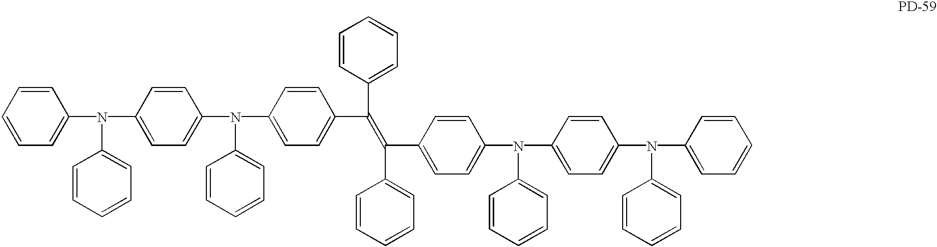


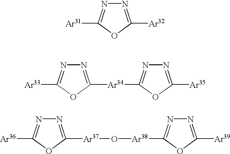


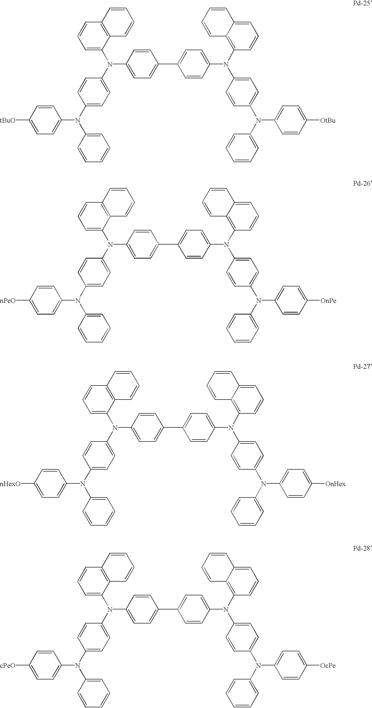


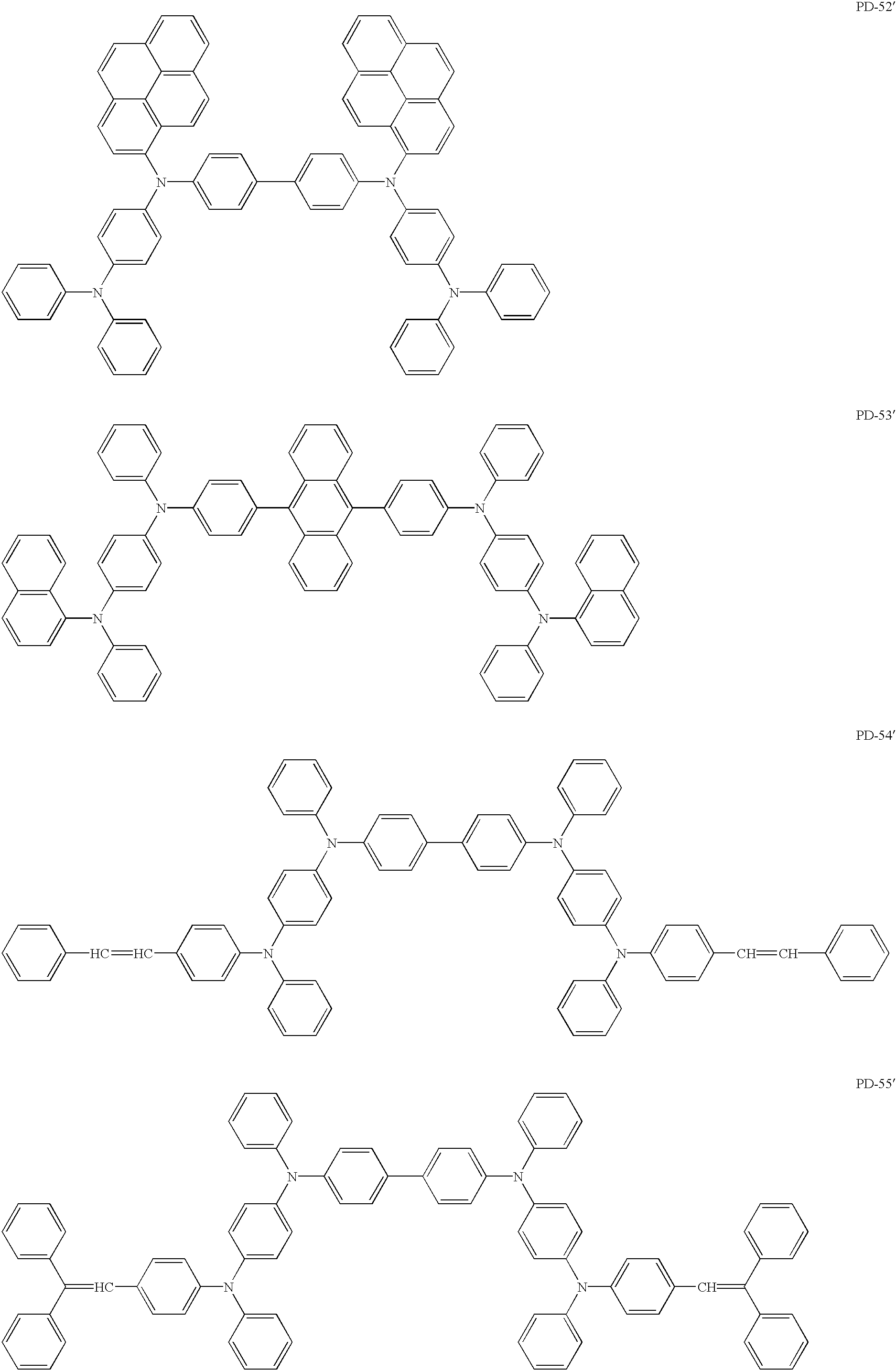


Claims (8)


Priority Applications (3)
| Application Number | Priority Date | Filing Date | Title |
|---|---|---|---|
| US10/331,645 US20030143430A1 (en) | 1998-09-09 | 2002-12-31 | Organic electroluminescence device and phenylenediamine derivative |
| US11/201,263 US7399537B2 (en) | 1998-09-09 | 2005-08-11 | Organic electroluminescence device and phenylenediamine derivative |
| US12/131,977 US20080241591A1 (en) | 1998-09-09 | 2008-06-03 | Organic electroluminescence device and phenylenediamine derivative |
Applications Claiming Priority (5)
| Application Number | Priority Date | Filing Date | Title |
|---|---|---|---|
| JP25556398 | 1998-09-09 | ||
| JP10-255563 | 1999-02-24 | ||
| JP11-047110 | 1999-02-24 | ||
| JP4711099 | 1999-02-24 | ||
| PCT/JP1999/004794 WO2000014174A1 (en) | 1998-09-09 | 1999-09-03 | Organic electroluminescence device and phenylenediamine derivative |
Related Parent Applications (1)
| Application Number | Title | Priority Date | Filing Date |
|---|---|---|---|
| PCT/JP1999/004794 A-371-Of-International WO2000014174A1 (en) | 1998-09-09 | 1999-09-03 | Organic electroluminescence device and phenylenediamine derivative |
Related Child Applications (1)
| Application Number | Title | Priority Date | Filing Date |
|---|---|---|---|
| US10/331,645 Division US20030143430A1 (en) | 1998-09-09 | 2002-12-31 | Organic electroluminescence device and phenylenediamine derivative |
Publications (1)
| Publication Number | Publication Date |
|---|---|
| US6541129B1 true US6541129B1 (en) | 2003-04-01 |
Family
ID=26387261
Family Applications (4)
| Application Number | Title | Priority Date | Filing Date |
|---|---|---|---|
| US09/530,597 Expired - Lifetime US6541129B1 (en) | 1998-09-09 | 1999-09-03 | Organic electroluminescence device and phenylenediamine derivative |
| US10/331,645 Pending US20030143430A1 (en) | 1998-09-09 | 2002-12-31 | Organic electroluminescence device and phenylenediamine derivative |
| US11/201,263 Expired - Fee Related US7399537B2 (en) | 1998-09-09 | 2005-08-11 | Organic electroluminescence device and phenylenediamine derivative |
| US12/131,977 Abandoned US20080241591A1 (en) | 1998-09-09 | 2008-06-03 | Organic electroluminescence device and phenylenediamine derivative |
Family Applications After (3)
| Application Number | Title | Priority Date | Filing Date |
|---|---|---|---|
| US10/331,645 Pending US20030143430A1 (en) | 1998-09-09 | 2002-12-31 | Organic electroluminescence device and phenylenediamine derivative |
| US11/201,263 Expired - Fee Related US7399537B2 (en) | 1998-09-09 | 2005-08-11 | Organic electroluminescence device and phenylenediamine derivative |
| US12/131,977 Abandoned US20080241591A1 (en) | 1998-09-09 | 2008-06-03 | Organic electroluminescence device and phenylenediamine derivative |
Country Status (6)
| Country | Link |
|---|---|
| US (4) | US6541129B1 (en) |
| EP (1) | EP1029909A4 (en) |
| KR (3) | KR100805451B1 (en) |
| CN (1) | CN1213127C (en) |
| TW (2) | TWI261583B (en) |
| WO (1) | WO2000014174A1 (en) |
Cited By (35)
| Publication number | Priority date | Publication date | Assignee | Title |
|---|---|---|---|---|
| US20020086180A1 (en) * | 2000-12-28 | 2002-07-04 | Satoshi Seo | Luminescent device |
| US20030030370A1 (en) * | 2001-08-13 | 2003-02-13 | Takumu Tada | Organic electroluminescence element and manufacturing method thereof |
| US20030143430A1 (en) * | 1998-09-09 | 2003-07-31 | Idemitsu Kosan Co., Ltd. | Organic electroluminescence device and phenylenediamine derivative |
| US20040076854A1 (en) * | 1999-12-20 | 2004-04-22 | Matsushita Electric Industrial Co., Ltd. | Thin film EL device |
| US20040110030A1 (en) * | 1996-12-28 | 2004-06-10 | Tdk Corporation | Organic EL device |
| US20050038296A1 (en) * | 1998-12-28 | 2005-02-17 | Idemitsu Kosan Co., Ltd. | Organic electrolumescence device |
| US20050065342A1 (en) * | 2003-07-28 | 2005-03-24 | Semiconductor Energy Laboratory Co., Ltd. | Quinoxaline derivatives, and light emitting element using thereof |
| US20050170737A1 (en) * | 2001-01-17 | 2005-08-04 | Semiconductor Energy Laboratory Co., Ltd., A Japan Corporation | Luminescent device and method of manufacturing same |
| US20050186446A1 (en) * | 2003-04-18 | 2005-08-25 | Semiconductor Energy Laboratory Co., Ltd. | Quinoxaline derivative, and organic semiconductor device, electric field light emitting device, and electronic device which have the same |
| US20050225235A1 (en) * | 2004-03-19 | 2005-10-13 | Kim Ji E | Materials for injecting or transporting holes and organic electroluminescence devices using the same |
| US20060061265A1 (en) * | 2002-11-06 | 2006-03-23 | Hisayuki Kawamura | Aromatic amine derivative and organic electroluminescent element employing the same |
| US20060232198A1 (en) * | 2005-04-18 | 2006-10-19 | Idemitsu Kosan Co., Ltd. | Aromatic triamine compound and organic electroluminescence device using the same |
| WO2006121237A1 (en) * | 2005-05-07 | 2006-11-16 | Doosan Corporation | Novel deuterated aryl amine compound, preparation method thereof, and organic light emitting diode using the same |
| US20070004280A1 (en) * | 2005-06-30 | 2007-01-04 | Hon Hai Precision Industry Co., Ltd. | Universal serial bus connector |
| US20070037011A1 (en) * | 2005-08-12 | 2007-02-15 | Semiconductor Energy Laboratory Co. | Arylamine compound and synthetic method thereof |
| US20070059553A1 (en) * | 2005-09-12 | 2007-03-15 | Semiconductor Energy Laboratory Co., Ltd. | Quinoxaline derivative, and light emitting element, light emitting device, and electronic appliance using the same |
| US20070152572A1 (en) * | 2004-11-26 | 2007-07-05 | Semiconductor Energy Laboratory Co., Ltd. | Light-emitting element, light-emitting device, and electronic device |
| US20070161793A1 (en) * | 2005-12-28 | 2007-07-12 | Hiroko Murata | Pyrazine derivative, and light emitting element, display device, electronic device using the pyrazine derivative |
| US20070222374A1 (en) * | 2006-03-21 | 2007-09-27 | Masakazu Egawa | Quinoxaline derivative, and light-emitting element, light-emitting device, electronic device using the quinoxaline derivative |
| US20070267969A1 (en) * | 2004-12-28 | 2007-11-22 | Harue Nakashima | Anthracene Derivative, Light Emitting Element Using the Same, and Light Emitting Device Using the Same |
| KR100799223B1 (en) | 2005-03-04 | 2008-01-29 | 에스케이씨 주식회사 | Hole injecting material and organic electroluminescent device comprising same |
| US20080074047A1 (en) * | 2006-09-22 | 2008-03-27 | Chung-Chun Lee | Tandem organic electroluminescent element and display use of the same |
| US20080136325A1 (en) * | 2005-02-28 | 2008-06-12 | Semiconductor Energy Laboratory Co., Ltd. | Composite Material, Light Emitting Element, Light Emitting Device and Electronic Appliance Using the Composite Material |
| US20090026928A1 (en) * | 2007-07-24 | 2009-01-29 | Samsung Electronics Co., Ltd. | Phenylphenoxazine or phenylphenothiazine- based compound and organic electroluminescent device using the same |
| US20090058267A1 (en) * | 2004-11-30 | 2009-03-05 | Semiconductor Energy Laboratory Co., Ltd. | Light emitting element and light emitting device |
| US20090072718A1 (en) * | 2007-02-28 | 2009-03-19 | Semiconductor Energy Laboratory Co., Ltd. | Quinoxaline derivative, and light-emitting element, light-emitting device, and electronic device including quinoxaline derivative |
| US20090140644A1 (en) * | 2007-12-03 | 2009-06-04 | Semiconductor Energy Laboratory Co., Ltd. | Quinoxaline Derivative, and Light-Emitting Element, Light-Emitting Device, and Electronic Device Using the Same |
| US20090160324A1 (en) * | 2007-12-21 | 2009-06-25 | Semiconductor Energy Laboratory Co., Ltd. | Triazole Derivative, Light-Emitting Element, Light-Emitting Device, and Electronic Device |
| US7564052B2 (en) | 2004-11-05 | 2009-07-21 | Semiconductor Energy Laboratory Co., Ltd. | Light-emitting element and light emitting device using the same |
| US20090230847A1 (en) * | 2005-07-25 | 2009-09-17 | Semiconductor Energy Laboratory Co., Ltd. | Light-Emitting Element, Light-Emitting Device, and Electronic Appliance |
| US7670506B1 (en) * | 2004-12-30 | 2010-03-02 | E. I. Du Pont De Nemours And Company | Photoactive compositions for liquid deposition |
| US8313845B2 (en) | 2009-03-31 | 2012-11-20 | Semiconductor Energy Laboratory Co., Ltd. | Quinoxaline derivative, and light-emitting element, light-emitting device, lighting device, and electronic device using quinoxaline derivative |
| US8974918B2 (en) | 2006-07-04 | 2015-03-10 | Semiconductor Energy Laboratory Co., Ltd. | Display device and electronic device |
| US10556864B2 (en) | 2007-12-03 | 2020-02-11 | Semiconductor Energy Laboratory Co., Ltd. | Carbazole derivative, and light-emitting element, light-emitting device, and electronic device using the carbazole derivative |
| US20220033342A1 (en) * | 2020-08-03 | 2022-02-03 | Ecole Polytechnique Federale De Lausanne (Epfl) | Hole transport material, synthesis thereof, and solar cell |
Families Citing this family (142)
| Publication number | Priority date | Publication date | Assignee | Title |
|---|---|---|---|---|
| KR100721656B1 (en) | 2005-11-01 | 2007-05-23 | 주식회사 엘지화학 | Organic electronic devices |
| CN100430515C (en) | 2001-02-01 | 2008-11-05 | 株式会社半导体能源研究所 | Sediment appts. and sediment method |
| SK9782003A3 (en) * | 2001-02-02 | 2004-01-08 | Schering Corp | 3,4-Di-substituted cyclobutene-1,2-diones as CXC chemokine receptor antagonists |
| GB0117377D0 (en) * | 2001-07-17 | 2001-09-05 | Opsys Ltd | "Tertiary diamines containing heterocyclic groups and their use in organic electroluminescent devices" |
| US6849345B2 (en) | 2001-09-28 | 2005-02-01 | Eastman Kodak Company | Organic electroluminescent devices with high luminance |
| US6610455B1 (en) | 2002-01-30 | 2003-08-26 | Eastman Kodak Company | Making electroluminscent display devices |
| US6872472B2 (en) | 2002-02-15 | 2005-03-29 | Eastman Kodak Company | Providing an organic electroluminescent device having stacked electroluminescent units |
| US6771021B2 (en) | 2002-05-28 | 2004-08-03 | Eastman Kodak Company | Lighting apparatus with flexible OLED area illumination light source and fixture |
| US6890627B2 (en) | 2002-08-02 | 2005-05-10 | Eastman Kodak Company | Laser thermal transfer from a donor element containing a hole-transporting layer |
| US6939660B2 (en) | 2002-08-02 | 2005-09-06 | Eastman Kodak Company | Laser thermal transfer donor including a separate dopant layer |
| US6747618B2 (en) | 2002-08-20 | 2004-06-08 | Eastman Kodak Company | Color organic light emitting diode display with improved lifetime |
| US6911961B2 (en) * | 2002-10-11 | 2005-06-28 | Eastman Kodak Company | Method of designing an OLED display with lifetime optimized primaries |
| US7230594B2 (en) | 2002-12-16 | 2007-06-12 | Eastman Kodak Company | Color OLED display with improved power efficiency |
| US7221332B2 (en) | 2003-12-19 | 2007-05-22 | Eastman Kodak Company | 3D stereo OLED display |
| DE102004020046A1 (en) * | 2003-12-22 | 2005-07-28 | Sensient Imaging Technologies Gmbh | New tris(diarylaminoaryl)amine derivatives, used as hole transport substance or luminescent substance in organic electroluminescent or electrophotographic device, have triaryl-methyl- or -silyl-aryl substituent(s) |
| US7541099B2 (en) * | 2004-05-21 | 2009-06-02 | Semiconductor Energy Laboratory Co., Ltd. | Anthracene derivative and light emitting element and light emitting device using the same |
| US7316756B2 (en) | 2004-07-27 | 2008-01-08 | Eastman Kodak Company | Desiccant for top-emitting OLED |
| US9040170B2 (en) | 2004-09-20 | 2015-05-26 | Global Oled Technology Llc | Electroluminescent device with quinazoline complex emitter |
| US7501151B2 (en) | 2004-09-21 | 2009-03-10 | Eastman Kodak Company | Delivering particulate material to a vaporization zone |
| US7501152B2 (en) | 2004-09-21 | 2009-03-10 | Eastman Kodak Company | Delivering particulate material to a vaporization zone |
| JPWO2006046441A1 (en) * | 2004-10-29 | 2008-05-22 | 出光興産株式会社 | Aromatic amine compound and organic electroluminescence device using the same |
| KR101210858B1 (en) * | 2004-11-05 | 2012-12-11 | 가부시키가이샤 한도오따이 에네루기 켄큐쇼 | Light emitting element and light emitting device using the same |
| JP4809666B2 (en) * | 2004-11-26 | 2011-11-09 | 株式会社半導体エネルギー研究所 | LIGHT EMITTING ELEMENT, LIGHT EMITTING DEVICE, AND ELECTRONIC DEVICE |
| EP1844005A4 (en) * | 2004-12-30 | 2010-07-28 | Du Pont | Charge transport materials |
| US8057916B2 (en) | 2005-04-20 | 2011-11-15 | Global Oled Technology, Llc. | OLED device with improved performance |
| KR100696528B1 (en) * | 2005-07-22 | 2007-03-19 | 삼성에스디아이 주식회사 | Triarylamine-based compound, preparing method thereof and Organic luminescence display device using the same |
| KR101479473B1 (en) * | 2005-09-02 | 2015-01-06 | 가부시키가이샤 한도오따이 에네루기 켄큐쇼 | Anthracene derivative |
| US8956738B2 (en) | 2005-10-26 | 2015-02-17 | Global Oled Technology Llc | Organic element for low voltage electroluminescent devices |
| US9666826B2 (en) | 2005-11-30 | 2017-05-30 | Global Oled Technology Llc | Electroluminescent device including an anthracene derivative |
| KR100845694B1 (en) | 2006-01-18 | 2008-07-11 | 주식회사 엘지화학 | Oled having stacked organic light-emitting units |
| US7799439B2 (en) | 2006-01-25 | 2010-09-21 | Global Oled Technology Llc | Fluorocarbon electrode modification layer |
| US9118020B2 (en) | 2006-04-27 | 2015-08-25 | Global Oled Technology Llc | Electroluminescent devices including organic eil layer |
| EP2355198B1 (en) | 2006-05-08 | 2015-09-09 | Global OLED Technology LLC | OLED electron-injecting layer |
| KR101422864B1 (en) | 2006-06-22 | 2014-07-24 | 소니 주식회사 | Organic electroluminescent device employing heterocycle-containing arylamine derivative |
| GB2440368A (en) | 2006-07-26 | 2008-01-30 | Oled T Ltd | Cathode coating for an electroluminescent device |
| KR101315379B1 (en) * | 2006-11-23 | 2013-10-10 | 삼성디스플레이 주식회사 | Manufacturing method of display device |
| DE102006059215A1 (en) | 2006-12-13 | 2008-07-10 | Sensient Imaging Technologies Gmbh | Arylamine-substituted divinylfluorenes and their use for electrophotographic applications and for OLEDS (Organic Light Emitting Devices) |
| GB0625540D0 (en) | 2006-12-22 | 2007-01-31 | Oled T Ltd | Electroluminescent devices |
| GB0625865D0 (en) | 2006-12-29 | 2007-02-07 | Oled T Ltd | Electro-optical or opto-electronic device |
| US8795855B2 (en) | 2007-01-30 | 2014-08-05 | Global Oled Technology Llc | OLEDs having high efficiency and excellent lifetime |
| JP2008258272A (en) * | 2007-04-02 | 2008-10-23 | Fuji Xerox Co Ltd | Organic electroluminescent element, and display unit |
| US7911133B2 (en) | 2007-05-10 | 2011-03-22 | Global Oled Technology Llc | Electroluminescent device having improved light output |
| US8034465B2 (en) | 2007-06-20 | 2011-10-11 | Global Oled Technology Llc | Phosphorescent oled having double exciton-blocking layers |
| US7812531B2 (en) | 2007-07-25 | 2010-10-12 | Global Oled Technology Llc | Preventing stress transfer in OLED display components |
| WO2009037155A1 (en) | 2007-09-20 | 2009-03-26 | Basf Se | Electroluminescent device |
| US8129039B2 (en) | 2007-10-26 | 2012-03-06 | Global Oled Technology, Llc | Phosphorescent OLED device with certain fluoranthene host |
| US8431242B2 (en) | 2007-10-26 | 2013-04-30 | Global Oled Technology, Llc. | OLED device with certain fluoranthene host |
| US8076009B2 (en) | 2007-10-26 | 2011-12-13 | Global Oled Technology, Llc. | OLED device with fluoranthene electron transport materials |
| US8420229B2 (en) | 2007-10-26 | 2013-04-16 | Global OLED Technologies LLC | OLED device with certain fluoranthene light-emitting dopants |
| US8016631B2 (en) | 2007-11-16 | 2011-09-13 | Global Oled Technology Llc | Desiccant sealing arrangement for OLED devices |
| US8900722B2 (en) | 2007-11-29 | 2014-12-02 | Global Oled Technology Llc | OLED device employing alkali metal cluster compounds |
| US8877350B2 (en) | 2007-12-11 | 2014-11-04 | Global Oled Technology Llc | White OLED with two blue light-emitting layers |
| CN101960636B (en) * | 2008-02-25 | 2012-07-18 | 昭和电工株式会社 | Organic electroluminescent element, and manufacturing method and uses therefor |
| GB0804469D0 (en) | 2008-03-11 | 2008-04-16 | Oled T Ltd | Compounds having electroluminescent or electron transport properties |
| US7947974B2 (en) | 2008-03-25 | 2011-05-24 | Global Oled Technology Llc | OLED device with hole-transport and electron-transport materials |
| JP5611538B2 (en) * | 2008-05-16 | 2014-10-22 | 株式会社半導体エネルギー研究所 | Benzoxazole derivative, and light-emitting element, light-emitting device, lighting device, and electronic device using benzoxazole derivative |
| US8324800B2 (en) | 2008-06-12 | 2012-12-04 | Global Oled Technology Llc | Phosphorescent OLED device with mixed hosts |
| US8247088B2 (en) | 2008-08-28 | 2012-08-21 | Global Oled Technology Llc | Emitting complex for electroluminescent devices |
| JP5459903B2 (en) * | 2008-09-02 | 2014-04-02 | 株式会社半導体エネルギー研究所 | Anthracene derivative, light emitting element, light emitting device, electronic device, and lighting device |
| EP2161272A1 (en) | 2008-09-05 | 2010-03-10 | Basf Se | Phenanthrolines |
| US7931975B2 (en) | 2008-11-07 | 2011-04-26 | Global Oled Technology Llc | Electroluminescent device containing a flouranthene compound |
| US8088500B2 (en) | 2008-11-12 | 2012-01-03 | Global Oled Technology Llc | OLED device with fluoranthene electron injection materials |
| US7968215B2 (en) | 2008-12-09 | 2011-06-28 | Global Oled Technology Llc | OLED device with cyclobutene electron injection materials |
| US8216697B2 (en) | 2009-02-13 | 2012-07-10 | Global Oled Technology Llc | OLED with fluoranthene-macrocyclic materials |
| US8147989B2 (en) | 2009-02-27 | 2012-04-03 | Global Oled Technology Llc | OLED device with stabilized green light-emitting layer |
| US8102114B2 (en) | 2009-02-27 | 2012-01-24 | Global Oled Technology, Llc. | Method of manufacturing an inverted bottom-emitting OLED device |
| US8283054B2 (en) | 2009-04-03 | 2012-10-09 | Global Oled Technology Llc | Tandem white OLED with efficient electron transfer |
| US8206842B2 (en) | 2009-04-06 | 2012-06-26 | Global Oled Technology Llc | Organic element for electroluminescent devices |
| EP2443213B1 (en) | 2009-06-18 | 2014-04-23 | Basf Se | Phenanthroazole compounds as hole transporting materials for electro luminescent devices |
| WO2011015265A2 (en) | 2009-08-04 | 2011-02-10 | Merck Patent Gmbh | Electronic devices comprising multi cyclic hydrocarbons |
| WO2011032686A1 (en) | 2009-09-16 | 2011-03-24 | Merck Patent Gmbh | Formulas for producing electronic devices |
| JP5897472B2 (en) | 2009-12-22 | 2016-03-30 | メルク パテント ゲーエムベーハー | Electroluminescent functional surfactant |
| EP2517278B1 (en) | 2009-12-22 | 2019-07-17 | Merck Patent GmbH | Electroluminescent formulations |
| EP2517275B1 (en) | 2009-12-22 | 2018-11-07 | Merck Patent GmbH | Formulations comprising phase-separated functional materials |
| EP2544765A1 (en) | 2010-03-11 | 2013-01-16 | Merck Patent GmbH | Fibers in therapy and cosmetics |
| JP2013522816A (en) | 2010-03-11 | 2013-06-13 | メルク パテント ゲーエムベーハー | Light emitting fiber |
| WO2011137922A1 (en) | 2010-05-03 | 2011-11-10 | Merck Patent Gmbh | Formulations and electronic devices |
| EP2576723B1 (en) | 2010-05-27 | 2017-09-20 | Merck Patent GmbH | Compositions comprising quantum dots |
| US8586206B2 (en) * | 2010-06-30 | 2013-11-19 | Idemitsu Kosan Co., Ltd. | Aromatic amine derivative and organic electroluminescence device using the same |
| CN103026525B (en) | 2010-07-26 | 2016-11-09 | 默克专利有限公司 | Nanocrystal in the devices |
| DE102010055901A1 (en) | 2010-12-23 | 2012-06-28 | Merck Patent Gmbh | Organic electroluminescent device |
| WO2012110178A1 (en) | 2011-02-14 | 2012-08-23 | Merck Patent Gmbh | Device and method for treatment of cells and cell tissue |
| EP2688646A1 (en) | 2011-03-24 | 2014-01-29 | Merck Patent GmbH | Organic ionic functional materials |
| WO2012152366A1 (en) | 2011-05-12 | 2012-11-15 | Merck Patent Gmbh | Organic ionic compounds, compositions and electronic devices |
| KR20140036279A (en) | 2011-06-01 | 2014-03-25 | 메르크 파텐트 게엠베하 | Hybrid ambipolar tfts |
| EP2737553A1 (en) | 2011-07-25 | 2014-06-04 | Merck Patent GmbH | Copolymers with functionalized side chains |
| DE102011117422A1 (en) | 2011-10-28 | 2013-05-02 | Merck Patent Gmbh | Hyperbranched polymers, process for their preparation and their use in electronic devices |
| US9263681B2 (en) | 2012-12-10 | 2016-02-16 | Nitto Denko Corporation | Organic light emitting host materials |
| WO2014099864A2 (en) | 2012-12-17 | 2014-06-26 | Nitto Denko Corporation | Light-emitting devices comprising emissive layer |
| GB201306365D0 (en) | 2013-04-09 | 2013-05-22 | Kathirgamanathan Poopathy | Heterocyclic compounds and their use in electro-optical or opto-electronic devices |
| US10593886B2 (en) | 2013-08-25 | 2020-03-17 | Molecular Glasses, Inc. | OLED devices with improved lifetime using non-crystallizable molecular glass mixture hosts |
| JP6601390B2 (en) * | 2014-03-14 | 2019-11-06 | 日産化学株式会社 | Aniline derivatives and uses thereof |
| WO2016034262A1 (en) | 2014-09-05 | 2016-03-10 | Merck Patent Gmbh | Formulations and electronic devices |
| EP3241248A1 (en) | 2014-12-30 | 2017-11-08 | Merck Patent GmbH | Formulations and electronic devices |
| JP6800879B2 (en) | 2015-03-30 | 2020-12-16 | メルク パテント ゲーエムベーハー | Formulations of organic functional materials containing siloxane solvents |
| KR101671277B1 (en) * | 2015-05-08 | 2016-11-01 | 머티어리얼사이언스 주식회사 | The method for manufacturing compound for organic electroluminescent device |
| EP3307846B1 (en) | 2015-06-12 | 2019-08-14 | Merck Patent GmbH | Esters containing non-aromatic cycles as solvents for oled formulations |
| JP2018527733A (en) | 2015-08-28 | 2018-09-20 | メルク パテント ゲーエムベーハー | Formulation of organic functional material containing epoxy group-containing solvent |
| WO2017097391A1 (en) | 2015-12-10 | 2017-06-15 | Merck Patent Gmbh | Formulations containing ketones comprising non-aromatic cycles |
| CN108369997B (en) | 2015-12-15 | 2020-03-24 | 默克专利有限公司 | Aromatic group-containing esters as solvents for organic electronic formulations |
| US11407916B2 (en) | 2015-12-16 | 2022-08-09 | Merck Patent Gmbh | Formulations containing a mixture of at least two different solvents |
| JP7438661B2 (en) | 2015-12-16 | 2024-02-27 | メルク パテント ゲーエムベーハー | Formulations containing solid solvents |
| EP3417033B1 (en) | 2016-02-17 | 2021-02-24 | Merck Patent GmbH | Formulation of an organic functional material |
| DE102016003104A1 (en) | 2016-03-15 | 2017-09-21 | Merck Patent Gmbh | Container comprising a formulation containing at least one organic semiconductor |
| KR20170124957A (en) * | 2016-05-03 | 2017-11-13 | 롬엔드하스전자재료코리아유한회사 | Organic electroluminescent compound and organic electroluminescent device comprising the same |
| JP2019523997A (en) | 2016-06-16 | 2019-08-29 | メルク パテント ゲーエムベーハー | Formulation of organic functional materials |
| EP3472249B1 (en) | 2016-06-17 | 2022-02-02 | Merck Patent GmbH | Formulation of an organic functional material |
| TW201815998A (en) | 2016-06-28 | 2018-05-01 | 德商麥克專利有限公司 | Formulation of an organic functional material |
| CN109563402B (en) | 2016-08-04 | 2022-07-15 | 默克专利有限公司 | Preparation of organic functional materials |
| KR102436600B1 (en) | 2016-10-31 | 2022-08-25 | 메르크 파텐트 게엠베하 | Formulation of organic functional materials |
| CN109863223B (en) | 2016-10-31 | 2023-06-20 | 默克专利有限公司 | Preparation of organic functional material |
| KR102472751B1 (en) | 2016-12-06 | 2022-11-30 | 메르크 파텐트 게엠베하 | Manufacturing method of electronic device |
| KR102486614B1 (en) | 2016-12-13 | 2023-01-09 | 메르크 파텐트 게엠베하 | Formulation of organic functional materials |
| WO2018114883A1 (en) | 2016-12-22 | 2018-06-28 | Merck Patent Gmbh | Mixtures comprising at least two organofunctional compounds |
| TWI763772B (en) | 2017-01-30 | 2022-05-11 | 德商麥克專利有限公司 | Method for forming an organic element of an electronic device |
| TWI791481B (en) | 2017-01-30 | 2023-02-11 | 德商麥克專利有限公司 | Method for forming an organic electroluminescence (el) element |
| JP7123967B2 (en) | 2017-03-31 | 2022-08-23 | メルク パテント ゲーエムベーハー | Printing method for organic light emitting diodes (OLEDs) |
| JP7200128B2 (en) | 2017-04-10 | 2023-01-06 | メルク パテント ゲーエムベーハー | Formulation of organic functional material |
| KR20200003068A (en) | 2017-05-03 | 2020-01-08 | 메르크 파텐트 게엠베하 | Formulations of Organic Functional Materials |
| WO2019016184A1 (en) | 2017-07-18 | 2019-01-24 | Merck Patent Gmbh | Formulation of an organic functional material |
| KR20200093653A (en) | 2017-12-15 | 2020-08-05 | 메르크 파텐트 게엠베하 | Formulation of organic functional materials |
| US20190237676A1 (en) | 2018-01-26 | 2019-08-01 | Samsung Display Co., Ltd. | Organic electroluminescence device and monoamine compound for organic electroluminescence device |
| US11871656B2 (en) | 2018-01-26 | 2024-01-09 | Samsung Display Co., Ltd. | Organic electroluminescence device and monoamine compound for organic electroluminescence device |
| CN111712551A (en) | 2018-02-26 | 2020-09-25 | 默克专利有限公司 | Preparation of organic functional material |
| KR102508497B1 (en) | 2018-03-26 | 2023-03-10 | 삼성디스플레이 주식회사 | Heterocyclic compound and organic light emitting device comprising the same |
| JP7379389B2 (en) | 2018-06-15 | 2023-11-14 | メルク パテント ゲーエムベーハー | Formulations of organic functional materials |
| KR102628848B1 (en) | 2018-08-10 | 2024-01-25 | 삼성디스플레이 주식회사 | Condensed compound and organic light-emitting device including the same |
| KR20210056432A (en) | 2018-09-24 | 2021-05-18 | 메르크 파텐트 게엠베하 | Method of manufacturing granular material |
| KR20210083347A (en) | 2018-11-06 | 2021-07-06 | 메르크 파텐트 게엠베하 | Method of Forming Organic Elements of Electronic Devices |
| US11043639B2 (en) | 2018-12-28 | 2021-06-22 | Samsung Electronics Co., Ltd. | Charge transport material, composition including the charge transport material, and organic light-emitting device including the composition |
| KR20200099249A (en) | 2019-02-13 | 2020-08-24 | 삼성디스플레이 주식회사 | Organic light emitting device |
| KR20200113057A (en) | 2019-03-20 | 2020-10-06 | 삼성디스플레이 주식회사 | AMINE-BASED compound and organic light emitting device comprising the same |
| KR20210038736A (en) | 2019-09-27 | 2021-04-08 | 삼성디스플레이 주식회사 | Condensed-cyclic compound and organic light emitting device including the same |
| CN111205237B (en) * | 2020-01-13 | 2020-12-29 | 长春海谱润斯科技股份有限公司 | Triamine derivative and organic electroluminescent device thereof |
| KR20230002860A (en) | 2020-04-21 | 2023-01-05 | 메르크 파텐트 게엠베하 | Emulsion containing organic functional materials |
| CN115867426A (en) | 2020-06-23 | 2023-03-28 | 默克专利有限公司 | Method for producing a mixture |
| JP2023552761A (en) | 2020-12-08 | 2023-12-19 | メルク パテント ゲーエムベーハー | Methods for ink-based and inkjet printing |
| EP4340969A1 (en) | 2021-05-21 | 2024-03-27 | Merck Patent GmbH | Method for the continuous purification of at least one functional material and device for the continuous purification of at least one functional material |
| CN117730638A (en) | 2021-08-02 | 2024-03-19 | 默克专利有限公司 | Printing method by combining inks |
| WO2023031073A1 (en) | 2021-08-31 | 2023-03-09 | Merck Patent Gmbh | Composition |
| TW202349760A (en) | 2021-10-05 | 2023-12-16 | 德商麥克專利有限公司 | Method for forming an organic element of an electronic device |
| WO2023237458A1 (en) | 2022-06-07 | 2023-12-14 | Merck Patent Gmbh | Method of printing a functional layer of an electronic device by combining inks |
Citations (13)
| Publication number | Priority date | Publication date | Assignee | Title |
|---|---|---|---|---|
| JPS62267749A (en) * | 1986-05-16 | 1987-11-20 | Fuji Xerox Co Ltd | Novel benzidine compound and its production |
| JPH0394262A (en) * | 1989-09-06 | 1991-04-19 | Konica Corp | Electrophotographic sensitive body |
| JPH0820771A (en) * | 1994-07-08 | 1996-01-23 | Toyo Ink Mfg Co Ltd | Hole-transporting material and its use |
| US5536949A (en) * | 1992-08-28 | 1996-07-16 | Idemistu Kosan Co., Ltd. | Charge injection auxiliary material and organic electroluminescence device containing the same |
| WO1996022273A1 (en) * | 1995-01-19 | 1996-07-25 | Idemitsu Kosan Co., Ltd. | Organic electroluminescent element, organic thin film, and triamine compounds |
| JPH08259934A (en) * | 1995-03-20 | 1996-10-08 | Matsushita Electric Ind Co Ltd | Electroluminescent element |
| JPH09301934A (en) * | 1996-05-10 | 1997-11-25 | Kemipuro Kasei Kk | High molecular weight aromatic amine compound and hole-transporting material |
| WO1998030071A1 (en) * | 1996-12-28 | 1998-07-09 | Tdk Corporation | Organic electroluminescent elements |
| JPH1154280A (en) * | 1997-07-31 | 1999-02-26 | Chisso Corp | Organic electroluminescent element using naphthylamine derivative |
| JPH11167992A (en) * | 1997-12-05 | 1999-06-22 | Mitsui Chem Inc | Organic electroluminescent element |
| US6259203B1 (en) * | 1997-07-31 | 2001-07-10 | Idemitsu Kosan Co., Ltd. | Organic electroluminescent device |
| US6406804B1 (en) * | 1998-04-09 | 2002-06-18 | Idemitsu Kosan Co., Ltd. | Organic electroluminescent device |
| US6437373B1 (en) * | 1998-05-08 | 2002-08-20 | Idemitsu Kosan Co., Ltd. | Organic electroluminescence layer with oligomer hole injection layer |
Family Cites Families (10)
| Publication number | Priority date | Publication date | Assignee | Title |
|---|---|---|---|---|
| EP0439627B1 (en) * | 1989-08-18 | 1996-07-10 | Idemitsu Kosan Company Limited | Organic electroluminescent element |
| JP3016896B2 (en) * | 1991-04-08 | 2000-03-06 | パイオニア株式会社 | Organic electroluminescence device |
| DE69432686T2 (en) | 1993-09-29 | 2004-03-18 | Idemitsu Kosan Co. Ltd. | Acrylenediamine derivatives and organic electroluminescent element containing them |
| JPH09222741A (en) * | 1995-12-11 | 1997-08-26 | Toyo Ink Mfg Co Ltd | Positive hole transferring material and its use |
| EP0857007B1 (en) * | 1996-08-19 | 2004-07-21 | TDK Corporation | Organic electroluminescent device |
| US5853905A (en) * | 1997-09-08 | 1998-12-29 | Motorola, Inc. | Efficient single layer electroluminescent device |
| US5853906A (en) * | 1997-10-14 | 1998-12-29 | Xerox Corporation | Conductive polymer compositions and processes thereof |
| WO2000014174A1 (en) * | 1998-09-09 | 2000-03-16 | Idemitsu Kosan Co., Ltd. | Organic electroluminescence device and phenylenediamine derivative |
| KR100702763B1 (en) * | 1999-02-15 | 2007-04-03 | 이데미쓰 고산 가부시키가이샤 | Organic electroluminescent device and method of manufacture thereof |
| JP3895178B2 (en) | 1999-09-30 | 2007-03-22 | 出光興産株式会社 | Amine compound and organic electroluminescence device using the same |
-
1999
- 1999-09-03 WO PCT/JP1999/004794 patent/WO2000014174A1/en active Application Filing
- 1999-09-03 KR KR1020067012880A patent/KR100805451B1/en not_active IP Right Cessation
- 1999-09-03 CN CNB998015229A patent/CN1213127C/en not_active Expired - Lifetime
- 1999-09-03 KR KR1020007004003A patent/KR100841842B1/en active IP Right Grant
- 1999-09-03 KR KR1020077012605A patent/KR100837029B1/en active IP Right Grant
- 1999-09-03 US US09/530,597 patent/US6541129B1/en not_active Expired - Lifetime
- 1999-09-03 EP EP99940653A patent/EP1029909A4/en not_active Withdrawn
- 1999-09-08 TW TW091117339A patent/TWI261583B/en not_active IP Right Cessation
- 1999-09-08 TW TW088115517A patent/TWI222965B/en not_active IP Right Cessation
-
2002
- 2002-12-31 US US10/331,645 patent/US20030143430A1/en active Pending
-
2005
- 2005-08-11 US US11/201,263 patent/US7399537B2/en not_active Expired - Fee Related
-
2008
- 2008-06-03 US US12/131,977 patent/US20080241591A1/en not_active Abandoned
Patent Citations (15)
| Publication number | Priority date | Publication date | Assignee | Title |
|---|---|---|---|---|
| JPS62267749A (en) * | 1986-05-16 | 1987-11-20 | Fuji Xerox Co Ltd | Novel benzidine compound and its production |
| JPH0394262A (en) * | 1989-09-06 | 1991-04-19 | Konica Corp | Electrophotographic sensitive body |
| US5536949A (en) * | 1992-08-28 | 1996-07-16 | Idemistu Kosan Co., Ltd. | Charge injection auxiliary material and organic electroluminescence device containing the same |
| JPH0820771A (en) * | 1994-07-08 | 1996-01-23 | Toyo Ink Mfg Co Ltd | Hole-transporting material and its use |
| WO1996022273A1 (en) * | 1995-01-19 | 1996-07-25 | Idemitsu Kosan Co., Ltd. | Organic electroluminescent element, organic thin film, and triamine compounds |
| JPH08259934A (en) * | 1995-03-20 | 1996-10-08 | Matsushita Electric Ind Co Ltd | Electroluminescent element |
| JPH09301934A (en) * | 1996-05-10 | 1997-11-25 | Kemipuro Kasei Kk | High molecular weight aromatic amine compound and hole-transporting material |
| WO1998030071A1 (en) * | 1996-12-28 | 1998-07-09 | Tdk Corporation | Organic electroluminescent elements |
| EP0891121A1 (en) | 1996-12-28 | 1999-01-13 | TDK Corporation | Organic electroluminescent elements |
| US6344283B1 (en) * | 1996-12-28 | 2002-02-05 | Tdk Corporation | Organic electroluminescent elements |
| JPH1154280A (en) * | 1997-07-31 | 1999-02-26 | Chisso Corp | Organic electroluminescent element using naphthylamine derivative |
| US6259203B1 (en) * | 1997-07-31 | 2001-07-10 | Idemitsu Kosan Co., Ltd. | Organic electroluminescent device |
| JPH11167992A (en) * | 1997-12-05 | 1999-06-22 | Mitsui Chem Inc | Organic electroluminescent element |
| US6406804B1 (en) * | 1998-04-09 | 2002-06-18 | Idemitsu Kosan Co., Ltd. | Organic electroluminescent device |
| US6437373B1 (en) * | 1998-05-08 | 2002-08-20 | Idemitsu Kosan Co., Ltd. | Organic electroluminescence layer with oligomer hole injection layer |
Non-Patent Citations (4)
| Title |
|---|
| U.S. patent application Ser. No. 09/121,831, filed Jul. 24, 1998, pending. |
| U.S. patent application Ser. No. 09/424,870, filed Dec. 9, 1999, pending. |
| U.S. patent application Ser. No. 09/446,905, filed Jan. 3, 2000, pending. |
| U.S. patent application Ser. No. 09/530,597, filed May 9, 2000, pending. |
Cited By (85)
| Publication number | Priority date | Publication date | Assignee | Title |
|---|---|---|---|---|
| US7097918B2 (en) * | 1996-12-28 | 2006-08-29 | Tdk Corporation | Organic EL device |
| US20040110030A1 (en) * | 1996-12-28 | 2004-06-10 | Tdk Corporation | Organic EL device |
| US20080241591A1 (en) * | 1998-09-09 | 2008-10-02 | Idemitsu Kosan Co., Ltd. | Organic electroluminescence device and phenylenediamine derivative |
| US20030143430A1 (en) * | 1998-09-09 | 2003-07-31 | Idemitsu Kosan Co., Ltd. | Organic electroluminescence device and phenylenediamine derivative |
| US7399537B2 (en) | 1998-09-09 | 2008-07-15 | Idemitsu Kosan Co., Ltd. | Organic electroluminescence device and phenylenediamine derivative |
| US20060082294A1 (en) * | 1998-09-09 | 2006-04-20 | Idemitsu Kosan Co., Ltd. | Organic electroluminescence device and phenylenediamine derivative |
| US20110175521A1 (en) * | 1998-12-28 | 2011-07-21 | Idemitsu Kosan Co., Ltd. | Organic electrolumescence device |
| US20070142671A1 (en) * | 1998-12-28 | 2007-06-21 | Idemitsu Kosan Co., Ltd | Organic electrolumescence device |
| US20050038296A1 (en) * | 1998-12-28 | 2005-02-17 | Idemitsu Kosan Co., Ltd. | Organic electrolumescence device |
| US20060189828A1 (en) * | 1998-12-28 | 2006-08-24 | Idemitsu Kosan Co., Ltd. | Organic electrolumescence device |
| US6989201B2 (en) | 1999-12-20 | 2006-01-24 | Matsushita Electric Industrial Co., Ltd. | Thin film EL device |
| US20040076854A1 (en) * | 1999-12-20 | 2004-04-22 | Matsushita Electric Industrial Co., Ltd. | Thin film EL device |
| US7579089B2 (en) | 2000-12-28 | 2009-08-25 | Semiconductor Energy Laboratory Co., Ltd. | Luminescent device |
| US20050260440A1 (en) * | 2000-12-28 | 2005-11-24 | Semiconductor Energy Laboratory Co., Ltd., A Japan Corporation | Luminescent device |
| US7572522B2 (en) | 2000-12-28 | 2009-08-11 | Semiconductor Energy Laboratory Co., Ltd. | Luminescent device |
| US8310147B2 (en) | 2000-12-28 | 2012-11-13 | Semiconductor Energy Laboratory Co., Ltd. | Luminescent device |
| US20020086180A1 (en) * | 2000-12-28 | 2002-07-04 | Satoshi Seo | Luminescent device |
| US20050170737A1 (en) * | 2001-01-17 | 2005-08-04 | Semiconductor Energy Laboratory Co., Ltd., A Japan Corporation | Luminescent device and method of manufacturing same |
| US7550173B2 (en) | 2001-01-17 | 2009-06-23 | Semiconductor Energy Laboratory Co., Ltd. | Luminescent device and method of manufacturing same |
| US6690109B2 (en) * | 2001-08-13 | 2004-02-10 | Victor Company Of Japan, Ltd. | Organic electroluminescence element and manufacturing method thereof |
| US20030030370A1 (en) * | 2001-08-13 | 2003-02-13 | Takumu Tada | Organic electroluminescence element and manufacturing method thereof |
| US20060061265A1 (en) * | 2002-11-06 | 2006-03-23 | Hisayuki Kawamura | Aromatic amine derivative and organic electroluminescent element employing the same |
| US20050186446A1 (en) * | 2003-04-18 | 2005-08-25 | Semiconductor Energy Laboratory Co., Ltd. | Quinoxaline derivative, and organic semiconductor device, electric field light emitting device, and electronic device which have the same |
| US8231984B2 (en) | 2003-04-18 | 2012-07-31 | Semiconductor Energy Laboratory Co., Ltd. | Quinoxaline derivative, and organic semiconductor device, electric field light emitting device, and electronic device which have the same |
| US7601435B2 (en) | 2003-04-18 | 2009-10-13 | Semiconductor Energy Laboratory Co., Ltd. | Quinoxaline derivative, and organic semiconductor device, electric field light emitting device, and electronic device which have the same |
| US8758905B2 (en) | 2003-04-18 | 2014-06-24 | Semiconductor Energy Laboratory Co., Ltd. | Quinoxaline derivative, and organic semiconductor device, electric field light emitting device, and electronic device which have the same |
| US20050065342A1 (en) * | 2003-07-28 | 2005-03-24 | Semiconductor Energy Laboratory Co., Ltd. | Quinoxaline derivatives, and light emitting element using thereof |
| US7245073B2 (en) | 2003-07-28 | 2007-07-17 | Semiconductor Energy Laboratory Co., Ltd. | Quinoxaline derivatives, and light emitting element using thereof |
| US8198801B2 (en) | 2004-03-19 | 2012-06-12 | Lg Chem, Ltd. | Materials for injecting or transporting holes and organic electroluminescence devices using the same |
| US20050225235A1 (en) * | 2004-03-19 | 2005-10-13 | Kim Ji E | Materials for injecting or transporting holes and organic electroluminescence devices using the same |
| US8207555B2 (en) | 2004-11-05 | 2012-06-26 | Semiconductor Energy Laboratory Co., Ltd. | Light-emitting element and light emitting device using the same |
| US8338196B2 (en) | 2004-11-05 | 2012-12-25 | Semiconductor Energy Laboratory Co., Ltd. | Light-emitting element and light emitting device using the same |
| US20090275161A1 (en) * | 2004-11-05 | 2009-11-05 | Semiconductor Energy Laboratory Co., Ltd. | Light-emitting element and light emitting device using the same |
| US7564052B2 (en) | 2004-11-05 | 2009-07-21 | Semiconductor Energy Laboratory Co., Ltd. | Light-emitting element and light emitting device using the same |
| US7646010B2 (en) * | 2004-11-26 | 2010-01-12 | Semiconductor Energy Laboratory Co., Ltd. | Light-emitting element, light-emitting device, and electronic device |
| US20070152572A1 (en) * | 2004-11-26 | 2007-07-05 | Semiconductor Energy Laboratory Co., Ltd. | Light-emitting element, light-emitting device, and electronic device |
| US9142783B2 (en) * | 2004-11-30 | 2015-09-22 | Semiconductor Energy Laboratory Co., Ltd. | Light emitting element and light emitting device |
| US20090058267A1 (en) * | 2004-11-30 | 2009-03-05 | Semiconductor Energy Laboratory Co., Ltd. | Light emitting element and light emitting device |
| US8815410B2 (en) | 2004-12-28 | 2014-08-26 | Semiconductor Energy Laboratory Co., Ltd. | Anthracene derivative, light emitting element using the same, and light emitting device using the same |
| US11296280B2 (en) | 2004-12-28 | 2022-04-05 | Semiconductor Energy Laboratory Co., Ltd. | Anthracene derivative, light emitting element using the same, and light emitting device using the same |
| US9478751B2 (en) | 2004-12-28 | 2016-10-25 | Semiconductor Energy Laboratory Co., Ltd. | Anthracene derivative, light emitting element using the same, and light emitting device using the same |
| US10326078B2 (en) | 2004-12-28 | 2019-06-18 | Semiconductor Energy Laboratory Co., Ltd. | Anthracene derivative, light-emitting element using the same, and light-emitting device using the same |
| US20070267969A1 (en) * | 2004-12-28 | 2007-11-22 | Harue Nakashima | Anthracene Derivative, Light Emitting Element Using the Same, and Light Emitting Device Using the Same |
| US7670506B1 (en) * | 2004-12-30 | 2010-03-02 | E. I. Du Pont De Nemours And Company | Photoactive compositions for liquid deposition |
| US20080136325A1 (en) * | 2005-02-28 | 2008-06-12 | Semiconductor Energy Laboratory Co., Ltd. | Composite Material, Light Emitting Element, Light Emitting Device and Electronic Appliance Using the Composite Material |
| US8586197B2 (en) | 2005-02-28 | 2013-11-19 | Semiconductor Energy Laboratory Co., Ltd. | Composite material, light emitting element, light emitting device and electronic appliance using the composite material |
| KR100799223B1 (en) | 2005-03-04 | 2008-01-29 | 에스케이씨 주식회사 | Hole injecting material and organic electroluminescent device comprising same |
| US20090115320A1 (en) * | 2005-04-18 | 2009-05-07 | Idemitsu Kosan Co., Ltd. | Aromatic triamine compound and organic electtroluminescence device using the same |
| US20060232198A1 (en) * | 2005-04-18 | 2006-10-19 | Idemitsu Kosan Co., Ltd. | Aromatic triamine compound and organic electroluminescence device using the same |
| US7425654B2 (en) * | 2005-04-18 | 2008-09-16 | Idemitsu Kosan Co., Ltd. | Aromatic triamine compound and organic electroluminescence device using the same |
| US20080191614A1 (en) * | 2005-05-07 | 2008-08-14 | Doosan Corporation | Novel Deuterated Aryl Amine Compound, Preparation Method Thereof, and Organic Light Emitting Diode Using The Same |
| WO2006121237A1 (en) * | 2005-05-07 | 2006-11-16 | Doosan Corporation | Novel deuterated aryl amine compound, preparation method thereof, and organic light emitting diode using the same |
| US8026665B2 (en) | 2005-05-07 | 2011-09-27 | Doosan Corporation | Deuterated aryl amine compound, preparation method thereof, and organic light emitting diode using the same |
| US20070004280A1 (en) * | 2005-06-30 | 2007-01-04 | Hon Hai Precision Industry Co., Ltd. | Universal serial bus connector |
| US20090230847A1 (en) * | 2005-07-25 | 2009-09-17 | Semiconductor Energy Laboratory Co., Ltd. | Light-Emitting Element, Light-Emitting Device, and Electronic Appliance |
| US8227982B2 (en) | 2005-07-25 | 2012-07-24 | Semiconductor Energy Laboratory Co., Ltd. | Light-emitting element, light-emitting device, and electronic appliance |
| US9224968B2 (en) | 2005-07-25 | 2015-12-29 | Semiconductor Energy Laboratory Co., Ltd. | Light-emitting element, light-emitting device, and electronic appliance |
| US20070037011A1 (en) * | 2005-08-12 | 2007-02-15 | Semiconductor Energy Laboratory Co. | Arylamine compound and synthetic method thereof |
| US8623523B2 (en) | 2005-09-12 | 2014-01-07 | Semiconductor Energy Laboratory Co., Ltd. | Quinoxaline derivative, and light emitting element, light emitting device, and electronic appliance using the same |
| US7901792B2 (en) | 2005-09-12 | 2011-03-08 | Semiconductor Energy Laboratory Co., Ltd. | Quinoxaline derivative, and light emitting element, light emitting device, and electronic appliance using the same |
| US8173277B2 (en) | 2005-09-12 | 2012-05-08 | Semiconductor Energy Laboratory Co., Ltd. | Quinoxaline derivative, and light-emitting element, light-emitting device, and electronic appliance using the same |
| US20110186825A1 (en) * | 2005-09-12 | 2011-08-04 | Semiconductor Energy Laboratory Co., Ltd. | Quinoxaline Derivative, and Light-Emitting Element, Light-Emitting Device, and Electronic Appliance Using the Same |
| US20070059553A1 (en) * | 2005-09-12 | 2007-03-15 | Semiconductor Energy Laboratory Co., Ltd. | Quinoxaline derivative, and light emitting element, light emitting device, and electronic appliance using the same |
| US20070161793A1 (en) * | 2005-12-28 | 2007-07-12 | Hiroko Murata | Pyrazine derivative, and light emitting element, display device, electronic device using the pyrazine derivative |
| US8920941B2 (en) * | 2005-12-28 | 2014-12-30 | Semiconductor Energy Laboratory Co., Ltd. | Pyrazine derivative, and light emitting element, display device, electronic device using the pyrazine derivative |
| US9324951B2 (en) | 2005-12-28 | 2016-04-26 | Semiconductor Energy Laboratory Co., Ltd. | Pyrazine derivative, and light emitting element, display device, electronic device using the pyrazine derivative |
| US20100141130A1 (en) * | 2006-03-21 | 2010-06-10 | Semiconductor Energy Laboratory Co., Ltd. | Quinoxaline derivative, and light-emitting element, light-emitting device, electronic device using the quinoxaline derivative |
| US7696348B2 (en) | 2006-03-21 | 2010-04-13 | Semiconductor Energy Laboratories Co., Ltd. | Quinoxaline derivative, and light-emitting element, light-emitting device, electronic device using the quinoxaline derivative |
| US8471017B2 (en) | 2006-03-21 | 2013-06-25 | Semiconductor Energy Laboratory Co. Ltd. | Quinoxaline derivative, and light-emitting element, light-emitting device, electronic device using the quinoxaline derivative |
| US8008489B2 (en) | 2006-03-21 | 2011-08-30 | Semiconductor Energy Laboratory Co., Ltd. | Quinoxaline derivative, and light-emitting element, light-emitting device, electronic device using the quinoxaline derivative |
| US20070222374A1 (en) * | 2006-03-21 | 2007-09-27 | Masakazu Egawa | Quinoxaline derivative, and light-emitting element, light-emitting device, electronic device using the quinoxaline derivative |
| US8974918B2 (en) | 2006-07-04 | 2015-03-10 | Semiconductor Energy Laboratory Co., Ltd. | Display device and electronic device |
| US20080074047A1 (en) * | 2006-09-22 | 2008-03-27 | Chung-Chun Lee | Tandem organic electroluminescent element and display use of the same |
| US8178216B2 (en) | 2007-02-28 | 2012-05-15 | Semiconductor Energy Laboratory Co., Ltd. | Quinoxaline derivative, and light-emitting element, light-emitting device, and electronic device including quinoxaline derivative |
| US20090072718A1 (en) * | 2007-02-28 | 2009-03-19 | Semiconductor Energy Laboratory Co., Ltd. | Quinoxaline derivative, and light-emitting element, light-emitting device, and electronic device including quinoxaline derivative |
| US7794858B2 (en) | 2007-07-24 | 2010-09-14 | Samsung Electronics Co., Ltd. | Phenylphenoxazine or phenylphenothiazine- based compound and organic electroluminescent device using the same |
| US20090026928A1 (en) * | 2007-07-24 | 2009-01-29 | Samsung Electronics Co., Ltd. | Phenylphenoxazine or phenylphenothiazine- based compound and organic electroluminescent device using the same |
| US20090140644A1 (en) * | 2007-12-03 | 2009-06-04 | Semiconductor Energy Laboratory Co., Ltd. | Quinoxaline Derivative, and Light-Emitting Element, Light-Emitting Device, and Electronic Device Using the Same |
| US7993761B2 (en) | 2007-12-03 | 2011-08-09 | Semiconductor Energy Laboratory Co., Ltd. | Quinoxaline derivative, and light-emitting element, light-emitting device, and electronic device using the same |
| US10556864B2 (en) | 2007-12-03 | 2020-02-11 | Semiconductor Energy Laboratory Co., Ltd. | Carbazole derivative, and light-emitting element, light-emitting device, and electronic device using the carbazole derivative |
| US8906518B2 (en) | 2007-12-21 | 2014-12-09 | Semiconductor Energy Laboratory Co., Ltd. | Triazole derivative, light-emitting element, light-emitting device, and electronic device |
| US20090160324A1 (en) * | 2007-12-21 | 2009-06-25 | Semiconductor Energy Laboratory Co., Ltd. | Triazole Derivative, Light-Emitting Element, Light-Emitting Device, and Electronic Device |
| US8313845B2 (en) | 2009-03-31 | 2012-11-20 | Semiconductor Energy Laboratory Co., Ltd. | Quinoxaline derivative, and light-emitting element, light-emitting device, lighting device, and electronic device using quinoxaline derivative |
| US20220033342A1 (en) * | 2020-08-03 | 2022-02-03 | Ecole Polytechnique Federale De Lausanne (Epfl) | Hole transport material, synthesis thereof, and solar cell |
| US11680035B2 (en) * | 2020-08-03 | 2023-06-20 | Ecole Polytechnique Federale De Lausanne (Epfl) | Hole transport material, synthesis thereof, and solar cell |
Also Published As
| Publication number | Publication date |
|---|---|
| US20080241591A1 (en) | 2008-10-02 |
| TWI222965B (en) | 2004-11-01 |
| US20030143430A1 (en) | 2003-07-31 |
| CN1277626A (en) | 2000-12-20 |
| KR20070073966A (en) | 2007-07-10 |
| KR20010031112A (en) | 2001-04-16 |
| KR20060085255A (en) | 2006-07-26 |
| EP1029909A4 (en) | 2007-01-10 |
| US20060082294A1 (en) | 2006-04-20 |
| KR100837029B1 (en) | 2008-06-10 |
| CN1213127C (en) | 2005-08-03 |
| US7399537B2 (en) | 2008-07-15 |
| EP1029909A1 (en) | 2000-08-23 |
| KR100841842B1 (en) | 2008-06-27 |
| WO2000014174A1 (en) | 2000-03-16 |
| TWI261583B (en) | 2006-09-11 |
| KR100805451B1 (en) | 2008-02-20 |
Similar Documents
| Publication | Publication Date | Title |
|---|---|---|
| US6541129B1 (en) | Organic electroluminescence device and phenylenediamine derivative | |
| EP1182183B1 (en) | Anthracene derivatives and organic electroluminescent devices made by using the same | |
| JP4542646B2 (en) | Organic electroluminescence device and phenylenediamine derivative | |
| US8137823B2 (en) | Anthracene derivatives, process for preparation thereof, and organic electronic light emitting device using the same | |
| JP4169085B2 (en) | Carbazole-containing amine compounds and uses thereof | |
| EP1136469B1 (en) | Organic electroluminescence element using an amine compound | |
| JP4211869B2 (en) | Diaminoarylene compound having carbazolyl group and use thereof | |
| US20060186799A1 (en) | Novel arylamine compound and organic electroluminescence device | |
| US8026514B2 (en) | Diamine derivatives and organic electronic device using the same | |
| US8173273B2 (en) | Anthracene derivatives, method for preparation thereof, and organic electronic device using the same | |
| WO2004083162A1 (en) | Aromatic amine derivative and organic electroluminescent element made with the same | |
| JP2000086595A (en) | Triphenylamine derivative and organic electroluminescent element using the same | |
| JP2007126439A (en) | Carbazole-containing amine compound and use thereof | |
| JP3251932B2 (en) | Novel diamine hole transfer material and organic electroluminescent device containing the same | |
| JP2000191560A (en) | Aromatic hydrocarbon compound and organic electroluminescence element using thereof | |
| JP2000192028A (en) | Aromatic hydrocarbon compound and organic electroluminescent element prepared by using the same | |
| JP2002175885A (en) | Organic electroluminescent element | |
| US20070243416A1 (en) | Amine Compound and Organic Electroluminescent Element Employing the Same | |
| JP4792687B2 (en) | Charge transport material, light-emitting material containing diazapentacene derivative, and organic electroluminescent device using the same | |
| JP2000186094A (en) | Silole compound and organic electroluminescent element using the same | |
| JP2004327455A (en) | Organic electroluminescent element | |
| JP2004327454A (en) | Organic electroluminescent element | |
| JP2000178549A (en) | Organic electroluminescence element |
Legal Events
| Date | Code | Title | Description |
|---|---|---|---|
| AS | Assignment |
Owner name: IDEMITSU KOSAN CO., LTD., JAPAN Free format text: ASSIGNMENT OF ASSIGNORS INTEREST;ASSIGNORS:KAWAMURA, HISAYUKI;HOSOKAWA, CHISHIO;REEL/FRAME:011042/0636 Effective date: 20000309 |
|
| STCF | Information on status: patent grant |
Free format text: PATENTED CASE |
|
| FEPP | Fee payment procedure |
Free format text: PAYOR NUMBER ASSIGNED (ORIGINAL EVENT CODE: ASPN); ENTITY STATUS OF PATENT OWNER: LARGE ENTITY Free format text: PAYER NUMBER DE-ASSIGNED (ORIGINAL EVENT CODE: RMPN); ENTITY STATUS OF PATENT OWNER: LARGE ENTITY |
|
| FPAY | Fee payment |
Year of fee payment: 4 |
|
| FPAY | Fee payment |
Year of fee payment: 8 |
|
| FPAY | Fee payment |
Year of fee payment: 12 |