US6542654B1 - Reconfigurable optical switch and method - Google Patents
Reconfigurable optical switch and method Download PDFInfo
- Publication number
- US6542654B1 US6542654B1 US09/902,908 US90290801A US6542654B1 US 6542654 B1 US6542654 B1 US 6542654B1 US 90290801 A US90290801 A US 90290801A US 6542654 B1 US6542654 B1 US 6542654B1
- Authority
- US
- United States
- Prior art keywords
- state
- crystal
- rods
- path
- rate
- Prior art date
- Legal status (The legal status is an assumption and is not a legal conclusion. Google has not performed a legal analysis and makes no representation as to the accuracy of the status listed.)
- Expired - Fee Related
Links
Images


Classifications
-
- G—PHYSICS
- G02—OPTICS
- G02F—OPTICAL DEVICES OR ARRANGEMENTS FOR THE CONTROL OF LIGHT BY MODIFICATION OF THE OPTICAL PROPERTIES OF THE MEDIA OF THE ELEMENTS INVOLVED THEREIN; NON-LINEAR OPTICS; FREQUENCY-CHANGING OF LIGHT; OPTICAL LOGIC ELEMENTS; OPTICAL ANALOGUE/DIGITAL CONVERTERS
- G02F1/00—Devices or arrangements for the control of the intensity, colour, phase, polarisation or direction of light arriving from an independent light source, e.g. switching, gating or modulating; Non-linear optics
- G02F1/29—Devices or arrangements for the control of the intensity, colour, phase, polarisation or direction of light arriving from an independent light source, e.g. switching, gating or modulating; Non-linear optics for the control of the position or the direction of light beams, i.e. deflection
- G02F1/31—Digital deflection, i.e. optical switching
- G02F1/313—Digital deflection, i.e. optical switching in an optical waveguide structure
-
- B—PERFORMING OPERATIONS; TRANSPORTING
- B82—NANOTECHNOLOGY
- B82Y—SPECIFIC USES OR APPLICATIONS OF NANOSTRUCTURES; MEASUREMENT OR ANALYSIS OF NANOSTRUCTURES; MANUFACTURE OR TREATMENT OF NANOSTRUCTURES
- B82Y20/00—Nanooptics, e.g. quantum optics or photonic crystals
-
- G—PHYSICS
- G02—OPTICS
- G02B—OPTICAL ELEMENTS, SYSTEMS OR APPARATUS
- G02B6/00—Light guides; Structural details of arrangements comprising light guides and other optical elements, e.g. couplings
- G02B6/10—Light guides; Structural details of arrangements comprising light guides and other optical elements, e.g. couplings of the optical waveguide type
- G02B6/12—Light guides; Structural details of arrangements comprising light guides and other optical elements, e.g. couplings of the optical waveguide type of the integrated circuit kind
- G02B6/122—Basic optical elements, e.g. light-guiding paths
- G02B6/1225—Basic optical elements, e.g. light-guiding paths comprising photonic band-gap structures or photonic lattices
-
- G—PHYSICS
- G02—OPTICS
- G02B—OPTICAL ELEMENTS, SYSTEMS OR APPARATUS
- G02B6/00—Light guides; Structural details of arrangements comprising light guides and other optical elements, e.g. couplings
- G02B6/10—Light guides; Structural details of arrangements comprising light guides and other optical elements, e.g. couplings of the optical waveguide type
- G02B6/12—Light guides; Structural details of arrangements comprising light guides and other optical elements, e.g. couplings of the optical waveguide type of the integrated circuit kind
- G02B2006/12133—Functions
- G02B2006/12145—Switch
-
- G—PHYSICS
- G02—OPTICS
- G02B—OPTICAL ELEMENTS, SYSTEMS OR APPARATUS
- G02B6/00—Light guides; Structural details of arrangements comprising light guides and other optical elements, e.g. couplings
- G02B6/24—Coupling light guides
- G02B6/26—Optical coupling means
- G02B6/35—Optical coupling means having switching means
- G02B6/354—Switching arrangements, i.e. number of input/output ports and interconnection types
- G02B6/3544—2D constellations, i.e. with switching elements and switched beams located in a plane
- G02B6/3548—1xN switch, i.e. one input and a selectable single output of N possible outputs
-
- G—PHYSICS
- G02—OPTICS
- G02B—OPTICAL ELEMENTS, SYSTEMS OR APPARATUS
- G02B6/00—Light guides; Structural details of arrangements comprising light guides and other optical elements, e.g. couplings
- G02B6/24—Coupling light guides
- G02B6/26—Optical coupling means
- G02B6/35—Optical coupling means having switching means
- G02B6/3594—Characterised by additional functional means, e.g. means for variably attenuating or branching or means for switching differently polarized beams
-
- G—PHYSICS
- G02—OPTICS
- G02F—OPTICAL DEVICES OR ARRANGEMENTS FOR THE CONTROL OF LIGHT BY MODIFICATION OF THE OPTICAL PROPERTIES OF THE MEDIA OF THE ELEMENTS INVOLVED THEREIN; NON-LINEAR OPTICS; FREQUENCY-CHANGING OF LIGHT; OPTICAL LOGIC ELEMENTS; OPTICAL ANALOGUE/DIGITAL CONVERTERS
- G02F1/00—Devices or arrangements for the control of the intensity, colour, phase, polarisation or direction of light arriving from an independent light source, e.g. switching, gating or modulating; Non-linear optics
- G02F1/01—Devices or arrangements for the control of the intensity, colour, phase, polarisation or direction of light arriving from an independent light source, e.g. switching, gating or modulating; Non-linear optics for the control of the intensity, phase, polarisation or colour
- G02F1/0147—Devices or arrangements for the control of the intensity, colour, phase, polarisation or direction of light arriving from an independent light source, e.g. switching, gating or modulating; Non-linear optics for the control of the intensity, phase, polarisation or colour based on thermo-optic effects
-
- G—PHYSICS
- G02—OPTICS
- G02F—OPTICAL DEVICES OR ARRANGEMENTS FOR THE CONTROL OF LIGHT BY MODIFICATION OF THE OPTICAL PROPERTIES OF THE MEDIA OF THE ELEMENTS INVOLVED THEREIN; NON-LINEAR OPTICS; FREQUENCY-CHANGING OF LIGHT; OPTICAL LOGIC ELEMENTS; OPTICAL ANALOGUE/DIGITAL CONVERTERS
- G02F2202/00—Materials and properties
- G02F2202/32—Photonic crystals
Definitions
- This application is related to:
- This invention relates generally to the field of optical devices, and more specifically to a reconfigurable optical switch and method.
- Photonic crystals may be used to manipulate light in optical devices, such as photonic bandgap devices.
- a photonic crystal typically includes regions periodically composed of materials with different refractive indices. The periodic changes in the refractive index of the crystal prevent light within a certain range or “band” of frequencies from entering or leaving the crystal. The band of frequencies that cannot propagate through the crystal may be referred to as a “bandgap.” To allow light within this band of frequencies to pass through certain paths in the photonic crystal, defects are created in the crystal. These defects represent points where the periodic changes in the refractive index of the crystal have been interrupted, which breaks the symmetry of the crystal. As a result of these defects, light may exist in localized states within the bandgap.
- Waveguides Sequences of defects allow light within the bandgap to propagate through the crystal in paths created by the defects. These paths may be referred to as “waveguides.”
- the waveguides control how light is transported through the crystal, so the waveguides control how the optical device operates.
- an optical switch in one embodiment, includes a photonic crystal and a controller.
- the photonic crystal includes a first path having a plurality of first regions. At least one of the first regions is set to a first state to allow an optical signal to propagate through at least a portion of the crystal.
- the photonic crystal also includes a second path having a plurality of second regions. At least one of the second regions is set to the first state.
- the photonic crystal further includes a third path coupling the first path and the second path and providing the optical signal for propagation through at least one of the first and second paths.
- the photonic crystal includes a first actuator coupled to at least one of the first regions, and a second actuator coupled to at least one of the second regions.
- the controller is coupled to the first and second actuators. The controller is operable to switch the first and second regions between the first state and a second state. The second state reduces the propagation of the optical signal through at least a portion of the crystal.
- a photonic crystal in another embodiment, includes a first path having a plurality of first regions. At least one of the first regions is set to a first state to allow an optical signal to propagate through at least a portion of the crystal.
- the photonic crystal also includes a second path having a plurality of second regions. At least one of the second regions is set to the first state.
- the photonic crystal further includes a third path coupling the first path and the second path and providing the optical signal for propagation through at least one of the first and second paths.
- the photonic crystal also includes a first actuator coupled to at least one of the first regions. The first actuator is operable to switch the first region between the first state and a second state. The second state reduces the propagation of the optical signal through at least a portion of the crystal.
- the photonic crystal includes a second actuator coupled to at least one of the second regions. The second actuator is operable to switch the second region between the first state and the second state.
- a method for reconfiguring an optical switch includes selecting a first path through a photonic crystal.
- the crystal includes the first path and a second path.
- the first path includes a plurality of first regions
- the second path includes a plurality of second regions.
- the crystal also includes a third path coupling the first path and the second path and providing an optical signal for propagation through one of the first and second paths.
- the method also includes heating at least one of the first regions and at least one of the second regions.
- the method further includes cooling the first region at a first rate to place the first region in a first state.
- the first state allows propagation of the optical signal through at least a portion of the crystal.
- the method includes cooling the second region at a second rate to place the second region in a second state. The second state reduces the propagation of the optical signal through at least a portion of the crystal.
- a photonic crystal includes rods of a material, such as a chalcogenide. At least one of the rods may switch between a first state and a second state. In the first state, a defect forms in the photonic crystal, and an optical signal may propagate through at least a portion of the crystal. In the second state, no defect forms around the rod, which reduces the propagation of the optical signal through at least a portion of the crystal.
- a defect may be formed by heating a rod and cooling the rod at one rate, and a defect may be removed by heating the rod and cooling the rod at another rate.
- the present invention may also allow the waveguides in the optical switch to be reconfigured more easily than conventional systems.
- the present invention may vary the refractive index of the rods to a greater degree than previous systems could achieve.
- the present invention may also change the refractive index of the rods faster than conventional systems.
- FIG. 1 is a block diagram illustrating an exemplary optical switch constructed according to the teachings of the present invention
- FIGS. 2A and 2B are block diagrams illustrating portions of an exemplary photonic crystal constructed according to the teachings of the present invention
- FIGS. 3A-3H are block diagrams illustrating an exemplary series of steps in manufacturing a photonic crystal
- FIGS. 4A and 4B are timing diagrams illustrating the reconfiguration of a photonic crystal according to the teachings of the present invention.
- FIG. 5 is a flow diagram illustrating an exemplary method for reconfiguring an optical switch according to the teachings of the present invention.
- FIG. 1 is a block diagram illustrating an exemplary optical switch 100 constructed according to the teachings of the present invention.
- switch 100 includes a photonic bandgap (PBG) crystal 102 and a controller 104 .
- PBG photonic bandgap
- Other embodiments of switch 100 may be used without departing from the scope of the present invention.
- crystal 102 contains waveguides 106 .
- Waveguides 106 represent areas of crystal 102 where light may exist in and propagate through defects in crystal 102 .
- crystal 102 includes one or more rods 108 operable to switch between at least a first state and a second state. Rods 108 that are operable to change states may be referred to as “switchable” rods.
- a defect exists in crystal 102 when rod 108 is in the first state, and light may exist in and propagate through the defect.
- a defect is removed from crystal 102 by switching rod 108 from the first state to the second state, which reduces or eliminates the propagation of light through that rod 108 .
- defects in crystal 102 may be formed by heating and cooling rod 108 at one rate, and defects may be removed in crystal 102 by heating and cooling rod 108 at another rate.
- crystal 102 may be reconfigured to perform different switching functions. For example, by reconfiguring waveguides 106 , switch 100 could reconfigure crystal 102 to route input signals from input lines 110 a - 110 b (referred to generally as input lines 110 ) to different output lines 112 a - 112 b (referred to generally as output lines 112 ).
- Other embodiments and/or uses of crystal 102 may be used without departing from the scope of the present invention.
- crystal 102 has been simplified to illustrate the various components of crystal 102 .
- crystal 102 may include any suitable number of waveguides 106 and rods 108 without departing from the scope of the present invention.
- crystal 102 may receive input signals from any number of input lines 110 and deliver optical signals to any number of output lines 112 .
- Crystal 102 is coupled to controller 104 .
- the term “couple” refers to any direct or indirect communication between two or more elements, whether or not those elements are in physical contact with one another.
- the term “crystal” refers to any structure or structures operable to receive and route optical signals, such as a photonic bandgap crystal.
- the term “photonic bandgap” refers to an ability to reduce or eliminate the propagation of light within a range or “band” of frequencies.
- Crystal 102 receives input optical signals from at least one input line 110 and routes the signals to one or more output lines 112 . The routing of signals from input line 110 to output line 112 is conducted by the waveguides 106 in crystal 102 .
- an input signal from input line 110 a may be routed to output line 112 a or output line 112 b, depending on which waveguide 106 is set to allow an optical signal to pass.
- crystal 102 may perform different switching functions in switch 100 .
- Crystal 102 may comprise any suitable structure operable to perform switching functions in switch 100 .
- FIGS. 2A and 2B One embodiment of a crystal is shown in FIGS. 2A and 2B, which are described below.
- crystal 102 includes a plurality of rods 108 .
- Rods 108 represent regions where the refractive index of the region may be altered to create and/or remove defects in crystal 102 .
- the term “rod” refers to any structure or structures having any suitable size, shape, and/or arrangement and operable to switch between at least a first state and a second state.
- the first state is associated with a refractive index that creates a defect in crystal 102
- the second state is associated with a refractive index that does not create a defect in crystal 102 .
- rod 108 may remain fixed or “latched” in one state until driven into another state.
- Rods 108 may comprise any suitable material or materials operable to switch between at least a first state and a second state.
- Rods 108 may, for example, comprise a chalcogenide, such as Ge 2 Sb 2 Te 5 .
- the chalcogenide may form part or all of rod 108 .
- the chalcogenide in rod 108 may exist in a different phase depending on whether the rod 108 is in the first state or second state. In a particular embodiment, when rod 108 is in the first state, the chalcogenide is in an amorphous or lower permittivity phase and forms a defect in crystal 102 .
- rod 108 When rod 108 is in the second state, the chalcogenide is in a polycrystalline or higher permittivity phase, and no defect exists at the point where rod 108 is located in crystal 102 .
- rod 108 may be polycrystalline in the first state and amorphous in the second state.
- Other state-phase combinations may be used without departing from the scope of the present invention.
- materials having other phases and/or states may be used in crystal 102 without departing from the scope of the present invention.
- the terms “higher” and “lower” refer to relative values and do not correspond to particular ranges of values.
- the phase of the rod 108 that creates a defect may depend, at least in part, on the phases of the other rods 108 in crystal 102 .
- a defect may be created in crystal 102 by changing at least one of the rods 108 to the amorphous phase.
- the rods 108 are in an amorphous phase, a defect may be created in crystal 102 by changing at least one of the rods 108 to the polycrystalline phase. While rods 108 may be described in other portions of this document as creating a defect in the amorphous phase, rods 108 may also create defects while in any other suitable phase.
- Input lines 110 are operable to provide an input optical signal to crystal 102
- output lines 112 are operable to receive an output optical signal from crystal 102 .
- the output signal received by output line 112 may be all or a portion of the input signal received by crystal 102 through input line 110 and routed through one or more waveguides 106 in crystal 102 .
- Input lines 110 and output lines 112 may comprise fibers, waveguides, free space coupling, focused optical beams, or any other structure operable to communicate optical energy.
- Input lines 110 and output lines 112 may have any suitable relationship between the lines.
- input lines 110 and output lines 112 may have a one-to-one relationship, where each input line 110 is associated with one output line 112 .
- Input lines 110 and output lines 112 may also have a one-to-many relationship, a many-to-one relationship, a many-to-many relationship, or any other suitable type of relationship.
- Controller 104 is coupled to crystal 102 . Controller 104 is operable to reconfigure crystal 102 by switching various rods 108 in crystal 102 between the first and second states of rods 108 .
- rods 108 in crystal 102 comprise a reversible phase-changeable chalcogenide, where a first phase creates a defect in crystal 102 and a second phase does not create a defect in crystal 102 .
- controller 104 may place a rod 108 in the first state by heating rod 108 and allowing rod 108 to cool at one rate. Controller 104 may also place a rod 108 in the second state by heating rod 108 and allowing rod 108 to cool at another rate.
- rod 108 is amorphous in the first state and polycrystalline in the second state.
- controller 104 may place rod 108 in the first state by heating rod 108 and allowing rod 108 to cool quickly, and controller 104 may place rod 108 in the second state by heating rod 108 and allowing rod 108 to cool gradually.
- the terms “quick” and “gradual” refer to relative time periods and are not meant to correspond to particular durations of time.
- controller 104 is described as changing the state of rod 108 by varying the heating and/or cooling rates of rod 108
- controller 104 may change the state of rod 108 and the optical characteristics of rod 108 using any other changes to the electrical and/or thermal profile of rod 108 .
- controller 104 may heat and/or cool a rod 108 by directly heating and/or cooling rod 108 , by activating appropriate elements in crystal 102 to heat and/or cool rod 108 , or in any other suitable manner.
- the terms “cool” and “cooling” include, but are not limited to, actively reducing the temperature of a rod 108 , and passively allowing the temperature of a rod 108 to fall.
- controller 104 may actively reduce the temperature of rod 108 by reducing the current flowing through rod 108 at a particular rate, and controller 104 may passively allow rod 108 to cool by eliminating the current flowing through rod 108 .
- Other methods of cooling rod 108 may be used without departing from the scope of the present invention.
- controller 104 may form different waveguides 106 in crystal 102 .
- Controller 104 may comprise any hardware, software, firmware, or combination thereof operable to reconfigure crystal 102 .
- controller 104 heats and cools a rod 108 in crystal 102 using an electric current.
- the electric current causes a rod 108 to heat, due to the resistance of rod 108 .
- the rate at which the rod 108 cools may depend on one or more characteristics of the current. For example, in one embodiment, a current having a larger amplitude and smaller duration may cause the rod 108 to cool quickly, while a current having a smaller amplitude and larger duration may cause the rod 108 to cool gradually. In this document, the terms “larger” and “smaller” refer to relative sizes and do not correspond to particular ranges of values.
- the rate at which the electric current is reduced controls the rate at which rod 108 cools.
- Controller 104 may control which state rod 108 enters by varying the characteristics of the electric current. For example, to cause rod 108 to become polycrystalline, the current controlled by controller 104 may cause rod 108 to cool gradually, such as between approximately ten to approximately fifty nanoseconds. To cause rod 108 to become amorphous, the current controlled by controller 104 causes rod 108 to cool quickly, such as between approximately one to approximately two nanoseconds. As a result, different waveguides 106 may be formed in crystal 102 by heating and cooling rods 108 at these different rates.
- Other embodiments of switch 100 may be used without departing from the scope of the present invention. For example, controller 104 could switch the states of rods 108 using an optical beam, such as from a laser, or any other suitable structure or structures operable to switch the states of rods 108 .
- Controller 104 may switch rods 108 in crystal 102 between the first and second states under the control of one or more input control signals received over control lines 114 .
- the control signals received over control lines 114 allow controller 104 to identify which rods 108 need to be in the first state and which rods 108 need to be in the second state.
- controller 104 includes a library 116 containing a plurality of entries. Each entry corresponds to a configuration of waveguides 106 in crystal 102 to achieve a mapping between one or more input lines 110 and one or more output lines 112 . For example, an entry may identify which rods 108 should be in the first and second states to establish particular waveguides 106 in crystal 102 .
- control signals received over control lines 114 identify the entry in library 116 that should be used to reconfigure crystal 102 .
- Controller 104 accesses library 116 , identifies the selected entry in library 116 , and retrieves the identity of the rods 108 that should be in the first and/or second states. After identifying the states of the rods 108 in crystal 102 , controller 104 may reconfigure crystal 102 .
- controller 104 may use an algorithm 118 to determine the states of rods 108 in crystal 102 .
- controller 104 processes the control signals using algorithm 118 .
- Algorithm 118 performs one or more operations on the control signals and identifies which rods 108 should be in the first state and/or the second state. After identifying the states of rods 108 , controller 104 may reconfigure crystal 102 . Other methods for identifying which rods 108 are to be placed in the first and second states may be used without departing from the scope of the present invention.
- Controller 104 may be coupled to crystal 102 by one or more signal lines 120 .
- Signal lines 120 are operable to transport signals, such as electric currents or optical signals used to reconfigure rods 108 , to and from crystal 102 .
- a switchable rod 108 may be coupled to at least two electrodes, and controller 104 may create a voltage differential across the electrodes using signal lines 120 .
- Signal lines 120 may comprise any suitable structure operable to communicate electrical signals used to reconfigure crystal 102 .
- FIG. 1 illustrates one example of an optical switch 100
- other embodiments of switch 100 may be used without departing from the scope of the present invention.
- any number of input lines 110 , output lines 112 , and control lines 114 may be used with switch 100 .
- any number of rods 108 may be switchable between different states.
- FIG. 1 illustrates controller 104 and crystal 102 as separate components of switch 100
- controller 104 and crystal 102 could be combined into a single component.
- controller 104 and crystal 102 may be fabricated on a single substrate using any suitable technique or techniques to provide an integral photonic device.
- FIGS. 2A and 2B are block diagrams illustrating portions of an exemplary photonic crystal 200 constructed according to the teachings of the present invention.
- Photonic crystal 200 may be useful, for example, in optical switch 100 of FIG. 1 .
- crystal 200 includes a plurality of rods 206 and a plurality of electrodes 204 .
- Other embodiments of crystal 200 may be used without departing from the scope of the present invention.
- Rods 206 represent areas of crystal 200 that may reduce or eliminate the propagation of an optical signal through crystal 200 or that may allow the optical signal to propagate through a defect in crystal 200 .
- at least one rod 206 a may be fixed in the second state. These rods 206 a reduce or eliminate the propagation of an optical signal through at least a portion of crystal 200 .
- At least one rod 206 b may also be fixed in the first state. These rods 206 b allow the propagation of the optical signal through at least a portion of crystal 200 .
- rods 206 a and rods 206 b have different refractive indices. In a particular embodiment, rods 206 a have a refractive index of approximately seven, and rods 206 b have a refractive index of approximately four. Other state-refractive index combinations may be used without departing from the scope of the present invention.
- At least one rod 206 in crystal 200 is a switchable rod.
- rod 206 c allows an optical signal to propagate through at least a portion of crystal 200
- rod 206 c reduces the propagation of the optical signal through crystal 200 .
- the two states of rod 206 c may correspond to different refractive indices of rod 206 c.
- the refractive index of rod 206 c may be the same or similar to the refractive index of rods 206 b.
- the refractive index of rod 206 c may be the same or similar to the refractive index of rods 206 a.
- Other materials having different refractive indices may be used without departing from the scope of the present invention.
- a series of rods 206 b form a waveguide 214 in crystal 200 .
- Waveguide 214 represents a path where optical signals may exist in and propagate through crystal 200 .
- An optical signal may propagate through waveguide 214 until reaching branch 216 .
- Branch 216 represents an area where waveguide 214 divides into two waveguides 218 a and 218 b.
- One or more switchable rods 206 c may make up the first portion of each waveguide 218 , and each waveguide 218 may also include one or more rods 206 b.
- the state of the switchable rods 206 c determines whether an optical signal propagating through waveguide 214 follows waveguide 218 a and/or waveguide 218 b.
- switchable rods 206 c in waveguide 218 a are amorphous while switchable rods 206 c in waveguide 218 b are polycrystalline
- optical signals would enter waveguide 218 a.
- Switchable rods 206 c in waveguide 218 b would reduce the propagation of the signals through waveguide 218 b.
- electrodes 204 would switch switchable rods 206 c in waveguide 218 a to the polycrystalline phase and switchable rods 206 c in waveguide 218 b to the amorphous phase.
- Optical signals would then enter waveguide 218 b, and switchable rods 206 c in waveguide 218 a would reduce the propagation of the signals through waveguide 218 a.
- Rods 206 a may surround at least a portion of waveguides 214 and 218 , which helps to conduct the optical signals through waveguides 214 and 218 and limit the conduction of the optical signals through other portions of crystal 200 . Because waveguides 218 may allow or reduce the propagation of optical signals based on the states of switchable rods 206 c, waveguides 218 may be referred to as “switchable” waveguides or paths.
- Rods 206 may comprise any suitable material or materials. In one embodiment, all rods 206 are composed of the same material operable to switch between at least a first state and a second state. In a particular embodiment, rods 206 comprise a reversible phase-changeable chalcogenide, such as Ge 2 Sb 2 Te 5 . In one embodiment, the material forming rod 206 a may be fixed in a higher-index phase, the material forming rod 206 b may be fixed in a lower-index phase, and the material forming rod 206 c may switch between phases.
- rods 206 a and 206 b may be fixed in the higher-index phase and the lower-index phase, respectively, many of the rods 206 in crystal 200 may be configured to operate in the first or second states during fabrication of crystal 200 . This may reduce the number of switchable rods 206 c in crystal 200 and simplify the operation of crystal 200 . This may also allow different waveguide geometries to be formed during fabrication of crystal 200 . For example, different waveguides can be formed in crystal 200 during fabrication by fixing at least some of the rods 206 in the lower-index or higher-index phases. At least one of the rods 206 may comprise a switchable rod 206 c, which may be switched between states to route optical signals through different waveguides in crystal 200 . Any suitable number of rods 206 a and 206 b may be fixed in the higher-index or lower-index phases, and any suitable number of rods 206 c may be switchable between states. In another embodiment, rods 206 may comprise different materials.
- Background material 208 separates rods 206 .
- Background material 208 may comprise any suitable material or materials in one or multiple layers.
- Background material 208 may, for example, comprise a dielectric material such as silicon dioxide or air.
- Electrodes 204 are coupled to at least one switchable rod 206 c. Electrodes 204 are operable to change the state of one or more rods 206 c. For example, in one embodiment, a defect may be formed in crystal 200 by heating and cooling rod 206 c at one rate, and defects in crystal 200 may be removed by heating and cooling rod 206 c at another rate. In a particular embodiment, rod 206 c may be heated using an electric current. The rate at which the rod 206 c cools may depend on one or more characteristics of the current, such as the amplitude, duration, and/or rate of reduction. In one embodiment, a pair of electrodes 204 a and 204 b may be coupled to a switchable rod 206 c.
- a voltage differential may be applied to the electrodes 204 a and 204 b, creating a current flowing through rod 206 c.
- the current generates heat due to the resistance of rod 206 c.
- rod 206 c is heated by applying a current for between approximately one and approximately two nanoseconds.
- rod 206 c is cooled at a rate of between approximately one and approximately two nanoseconds. This may form a defect in crystal 200 .
- rod 206 c is cooled at a rate of between approximately ten and approximately fifty nanoseconds. This may remove a defect from crystal 200 .
- Electrodes 204 may comprise any suitable material or materials in one or multiple layers. Electrodes 204 may, for example, comprise copper, gold, silver, and/or doped polysilicon. Although FIG. 2A illustrates one electrode 204 a coupled to each rod 206 c and one electrode 204 b coupled to three rods 206 c, other embodiments of crystal 200 may be used without departing from the scope of the present invention. For example, electrode 204 and/or electrode 204 b may be coupled to any number of switchable rods 206 c.
- the arrangement, size, and shape of rods 206 and the refractive indices of the materials in crystal 200 determine the optical characteristics of crystal 200 .
- crystal 200 prevents light within a certain range or band of frequencies from propagating through crystal 200 , unless a defect is formed in crystal 200 .
- the center of the frequency range depends, at least in part, on the center-to-center distance 219 of rods 206 . In one embodiment, distance 219 is approximately 0.5 micrometers.
- a crystal 200 may be constructed having properties suitable for a particular application.
- a crystal 200 having normalized bandgaps of fifteen to twenty-five percent or more is achievable, and localized states may exist near the center of the bandgaps.
- the center-to-center distance 219 of rods 206 is 0.5 micrometers
- the radius of rods 206 is 0.11 micrometers
- the height of rods 206 is 0.6 micrometers
- the thickness of cladding 210 is 3 micrometers. This provides a normalized bandgap of approximately fifteen percent.
- the center-to-center distance 219 of rods 206 is 0.5 micrometers, the radius of rods 206 is 0.08 micrometers, the height of rods 206 is 0.9 micrometers, and the thickness of cladding 210 is 3 micrometers. This provides a normalized bandgap of approximately twenty-five percent.
- Other embodiments of crystal 200 may be used without departing from the scope of the present invention.
- crystal 200 in FIG. 2A has a single branch 216 dividing waveguide 214 into two waveguides 218 , crystal 200 acts as a 1 ⁇ 2 optical switch.
- An input signal may take one of two paths through crystal 200 .
- Cascading the 1 ⁇ 2 switches produces a 1 ⁇ N switch, meaning that an input signal may take one of N paths through the switch.
- Cascading N 1 ⁇ N switches in parallel produces half of a N ⁇ N switch.
- each 1 ⁇ 2 switch may occupy less than 10 square micrometers of space, and up to one million 1 ⁇ 2 switches may be placed in a square centimeter.
- FIG. 2B illustrates the cross-section of crystal 200 along line A—A in FIG. 2 A.
- crystal 200 includes a waveguide area 202 and two electrodes 204 a and 204 b.
- Waveguide area 202 represents the area of crystal 200 where optical signals may be guided through waveguides in crystal 200 .
- waveguide area 202 includes rods 206 , background material 208 , and a confinement cladding 210 disposed around rods 206 .
- confinement claddings 210 a and 210 b are disposed on top and bottom of rods 206 .
- Each confinement cladding 210 may confine optical signals traveling through crystal 200 to the region 212 in which rods 206 are located. This helps to prevent the optical signals from radiating out of crystal 200 .
- Confinement cladding 210 may comprise any suitable material or materials in one or multiple layers.
- confinement cladding 210 comprises the same material as background material 208 , such as silicon dioxide.
- confinement cladding 210 and background material 208 comprise different materials.
- confinement cladding 210 may have a refractive index that is less than or equal to the refractive index of background material 208 .
- Electrodes 204 a and 204 b may have any suitable size and/or shape in crystal 200 .
- each electrode 204 protrudes through a confinement cladding 210 in order to contact rod 206 c.
- the use of a protruding electrode 204 may help to reduce the perturbation of crystal 200 caused by the presence of a conductive material within waveguide area 202 of crystal 200 .
- Other electrodes 204 may be used without departing from the scope of the present invention.
- the crystal 200 illustrated in FIGS. 2A and 2B may be formed by any suitable process or processes.
- rods 206 in crystal 200 may be formed using interference lithography.
- one or more rods 206 may be fixed in the first state and one or more rods 206 may be fixed in the second state.
- different waveguides 214 and 218 may be formed in crystal 200 .
- One or more electrodes 204 may also be formed in crystal 200 , and electrodes 204 may be used to switch one or more rods 206 between the first and second states. By overlaying the electrodes on switchable rods 206 , the waveguides in crystal 200 may be reconfigured.
- FIGS. 2A and 2B illustrate one embodiment of crystal 200
- any suitable number of waveguides 214 , branches 216 , and waveguides 218 may be used in crystal 200 .
- Any number of rods 206 may be used in crystal 200 , and any number of rods 206 may be fixed in the first state and/or the second state.
- any number of rods 206 may comprise switchable rods 206 c, and any suitable number of switchable rods 206 c may be used to block waveguides 218 in crystal 200 .
- FIG. 2A illustrates rods 206 arranged in a triangular lattice within a planar region 212 of crystal 200
- other arrangements such as rectangular and honeycomb lattices, may be used in crystal 200
- other methods may be used to change the state of rods 206 c in place of electrodes 204 .
- one or more Vertical Cavity Surface Emitting Lasers (VCSEL) and focusing lenses to target the lasers may be used to change the state of rods 206 c.
- VCSEL Vertical Cavity Surface Emitting Lasers
- Other changes may be used without departing from the scope of the present invention.
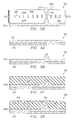
- FIGS. 3A-3H are block diagrams illustrating an exemplary series of steps in manufacturing a photonic crystal 300 .
- the steps shown in FIGS. 3A-3H are for illustration only. Other fabrication methods may be used without departing from the scope of the present invention.
- a layer 322 of a conductive material is deposited on a substrate 320 .
- Substrate 320 may comprise any suitable material or materials in one or multiple layers, such as a layer of silicon.
- Layer 322 may comprise any suitable conductive material or materials in one or multiple layers, such as a layer of gold, silver, copper, and/or doped polysilicon. Layer 322 may be deposited on substrate 320 using any suitable method.
- layer 322 is formed into the shape of an electrode 304 b. Any suitable method, such as a pattern and etch, may be used to form electrode 304 b.
- a layer 324 of a dielectric material is deposited on electrode 304 b.
- Layer 324 may comprise any suitable dielectric material or materials in one or multiple layers, such as a layer of silicon dioxide.
- Layer 324 may be formed using any suitable method, such as chemical vapor deposition.
- layer 324 is planarized, and a plurality of cavities 326 are formed in layer 324 .
- the cavities 326 may be formed to approximately conform to the shape of rods 206 . Cavities 326 could also be formed to any other suitable shape in crystal 300 . Cavities 326 may be formed in layer 324 using any suitable method, such as a pattern and etch, a photomask, or a three-beam interference lithography technique. Cavities 326 may have any suitable geometric pattern, such as a triangular, rectangular, or honeycomb lattice.
- rods 306 are formed in cavities 326 .
- Rods 306 may, for example, be formed by depositing a layer of a chalcogenide in cavities 326 and then planarizing the material. This forms rods 306 separated by dielectric material 308 and a confinement cladding 310 b disposed under rods 306 .
- FIG. 3E illustrates the material from layer 324 separating rods 306 , a different material than layer 324 could also be used.
- layer 324 could be planarized, an additional material could be disposed on layer 324 , and cavities 326 could be formed in the additional layer.
- rods 306 may be placed into the first state or the second state at this point.
- rods 306 a could be placed in the second state.
- Switchable rods 306 c may or may not be initially placed in the first or second states at this step or later.
- Rods 306 could be placed in one of the states through laser irradiation or any other suitable method.
- a layer 328 of a dielectric material is deposited on rods 306 .
- Layer 328 may comprise any suitable dielectric material or materials in one or multiple layers, such as a layer of silicon dioxide.
- Layer 328 may be formed using any suitable method, such as chemical vapor deposition.
- a cavity 330 is formed in layer 328 .
- the cavity 330 may be formed to approximately conform to the shape of electrode 204 a.
- Cavity 330 may be formed in layer 328 using any suitable method, such as a pattern and etch.
- electrode 304 a is formed in cavity 330 .
- Electrode 304 a may be formed, for example, by depositing a conductive material in and around cavity 330 and forming the material into electrode 304 a.
- FIGS. 3A-3H illustrate an exemplary series of steps in the formation of a photonic crystal 300
- various changes may be made to the series of steps without departing from the scope of the present invention.
- an optical device may use one or more lasers to switch switchable rods 306 c from one state to another, and electrodes 304 need not be formed in crystal 300 .
- other suitable fabrication techniques may be used to form crystal 300 without departing from the scope of the present invention.
- FIGS. 4A and 4B are timing diagrams illustrating the reconfiguration of a photonic crystal according to the teachings of the present invention. Although FIGS. 4A and 4B are described with respect to crystal 200 of FIGS. 2A and 2B, the same or similar timing may be used in crystal 102 of FIG. 1, crystal 300 of FIGS. 3A through 3H, and any other suitable photonic crystal.
- timing diagram 400 illustrates how a current applied to a rod 206 changes the temperature of rod 206 , which causes a change in the phase of the material forming rod 206 .
- the current applied to rod 206 may, for example, be delivered to rod 206 by a controller, such as controller 104 , through one or more signal lines 120 and associated electrodes 204 .
- the material in rod 206 may have a first phase 402 , which creates a defect in crystal 200 , and a second phase 404 , which does not form a defect in crystal 200 .
- a rod 206 in the first phase 402 is amorphous
- a rod 206 in the second phase 404 is polycrystalline.
- Other phase-defect combinations may be used without departing from the scope of the present invention.
- a current 406 is applied to rod 206 for a time 408 .
- This may include, for example, a controller such as controller 104 providing a square wave to one of the electrodes 204 coupled to rod 206 .
- current 406 is applied to rod 206 for a time 408 of between one to two nanoseconds.
- the amplitude of current 406 may depend, at least in part, on the amount of material forming rod 206 .
- Current 406 increases the temperature 410 of rod 206 during a time 412 .
- Time 412 may, for example, be between one and two nanoseconds.
- current 406 increases temperature 410 of rod 206 to the melting point of rod 206 .
- rod 206 comprises a chalcogenide such as Ge 2 Sb 2 Te 5 , and current 406 heats rod 206 to at least 620° Centigrade. This causes the material in rod 206 to enter a third phase 405 in which the material in rod 206 becomes liquid. After time 412 , the temperature 410 of rod 206 decreases during a time 414 . In one embodiment, time 414 represents a time of one to two nanoseconds. Because the temperature 410 of rod 206 falls quickly, the material in rod 206 enters the first phase 402 , and a defect is formed in crystal 200 .
- a current 416 is applied to rod 206 for a time 418 .
- This may include controller 104 providing a square wave to one of the electrodes 204 coupled to rod 206 .
- current 416 is applied to rod 206 for a time 418 of between ten to fifty nanoseconds.
- Current 416 increases the temperature 420 of rod 206 during a time 422 .
- Time 422 may, for example, be between one and two nanoseconds. This may cause the material in rod 206 to enter the liquid phase 405 .
- the temperature 420 of rod 206 then decreases during a time 424 .
- time 424 represents a time of ten to fifty nanoseconds. This reduces the temperature 420 of rod 206 gradually, placing the material in rod 206 in the second phase 404 . As a result, no defect is formed in crystal 200 at the location of rod 206 .
- timing diagram 450 illustrates how another current applied to rod 206 changes the temperature of rod 206 and the phase of the material forming rod 206 .
- Rod 206 may have a first phase 452 , which creates a defect in crystal 200 , and a second phase 454 , which does not form a defect in crystal 200 .
- rod 206 is amorphous in the first phase 452 and polycrystalline in the second phase 454 .
- Other phase-defect combinations may be used without departing from the scope of the present invention.
- a current 456 is applied to rod 206 for a time 458 .
- This may include, for example, creating a voltage differential between the electrodes 204 coupled to rod 206 to establish current 456 through rod 206 .
- current 456 is reduced during a time 460 .
- time 458 and time 460 each represents a period of one to two nanoseconds.
- the amplitude of current 456 may depend, at least in part, on the amount of material forming rod 206 .
- Current 456 causes the temperature 462 of rod 206 to increase during a time 464 and then decrease during time 466 .
- current 456 increases temperature 462 of rod 206 to the point where the material in rod 206 melts and enters a liquid phase 455 .
- time 464 and time 466 each represents a time of one to two nanoseconds. Because the temperature 462 of rod 206 falls quickly, the material in rod 206 enters the first phase 452 , and a defect is formed in crystal 200 .
- a current 468 is applied to rod 206 for a time 470 , and current 468 is reduced during a time 472 .
- time 470 represents a period of one to two nanoseconds
- time 472 represents a time of ten to fifty nanoseconds.
- Current 468 causes the temperature 474 of rod 206 to increase during a time 476 and then decrease during time 478 .
- time 476 represents a period of one to two nanoseconds
- time 478 represents a period of ten to fifty nanoseconds.
- the current 468 causes the material in rod 206 to enter the liquid phase 455 , and the gradual reduction in temperature 474 of rod 206 causes the material in rod 206 to enter the second phase 454 . As a result, no defect is formed at rod 206 in crystal 200 .
- FIGS. 4A and 4B illustrate example currents that may be used to reconfigure a rod 206
- various changes may be made to FIGS. 4A and 4B without departing from the scope of the present invention.
- the currents, times, temperatures, and phases shown in FIGS. 4A and 4B are for illustration only. Other and/or additional currents, times, temperatures, and/or phases may be used without departing from the scope of the present invention.
- the material in rods 206 is shown to have three phases, rods 206 may be formed from a material having any suitable number of phases.
- any suitable currents may be used to heat rods 206 and/or cool rods 206 . In one embodiment, any currents operable to allow rod 206 to cool at different rates and enter different phases may be used without departing from the scope of the present invention.
- FIG. 5 is a flow diagram illustrating an exemplary method 500 for reconfiguring an optical switch according to the teachings of the present invention. Although FIG. 5 is described with respect to crystal 200 of FIGS. 2A and 2B, the same or similar method may be used by switch 100 of FIG. 1, crystal 300 of FIGS. 3A through 3H, or any other suitable optical switch.
- a controller or other logic determines the desired path through crystal 200 at step 502 . This may include, for example, determining how an optical signal is to be routed through the waveguides 214 and 218 in crystal 200 .
- the controller or other logic determines if crystal 200 is configured correctly at step 504 . This may include, for example, determining if a waveguide 214 branches toward the desired waveguide 218 in crystal 200 .
- controller 104 retrieves a path-to-rod mapping from memory at step 505 .
- the path-to-rod mapping may, for example, be stored as an entry in library 116 or computed by algorithm 118 .
- Controller 104 heats the switchable rods 206 c along the desired path in crystal 200 at step 506 .
- the desired path may represent one of the waveguides 218 that travels through crystal 200 in the proper direction, such as a waveguide 218 leading toward the final destination of the optical signal.
- the switchable rods 206 c along the desired path may be heated, for example, by applying a current to the rods 206 c through the electrodes 204 coupled to the rods 206 c.
- the current may last for any suitable length of time, such as one to two nanoseconds.
- the switchable rods 206 c along the desired path are cooled quickly at step 508 .
- This may include, for example, controller 104 cooling the rods 206 c quickly by controlling at least one of the duration of the current, the amplitude of the current, and the rate at which the current is reduced. Because of the quick cooling rate, switchable rods 206 c enter the first state at step 510 .
- the material that forms rods 206 c may, for example, enter an amorphous phase, and defects form at the locations of switchable rods 206 c. This reconfigures crystal 200 by opening the desired path through crystal 200 .
- Controller 104 also heats the switchable rods 206 c along the undesired path in crystal 200 at step 512 .
- the undesired path may represent one of the waveguides 218 that travels through crystal 200 in an improper direction, such as a waveguide 218 that diverges from the desired path and leads away from the final destination of the optical signal.
- the switchable rods 206 c along the undesired path may be heated, for example, by applying a current to the rods 206 c.
- the switchable rods 206 c along the undesired path are cooled gradually at step 514 .
- This may include, for example, controller 104 cooling the rods 206 c gradually by controlling at least one of the duration of the current, the amplitude of the current, and the rate at which the current is reduced. Because of the gradual cooling rate, switchable rods 206 c enter the second state at step 516 .
- the material that forms rods 206 c may, for example, enter a polycrystalline phase, and defects are removed from crystal 200 . This reconfigures crystal 200 by closing the undesired paths through crystal 200 . At this point, crystal 200 has been reconfigured to guide an optical signal in a desired path through crystal 200 . At a branch 216 in crystal 200 , the desired path has been opened and the undesired path has been closed.
- FIG. 5 illustrates one example of a method 500 for reconfiguring an optical switch
- various changes may be made to method 500 without departing from the scope of the present invention.
- FIG. 5 illustrates a series of steps 506 - 516 to reconfigure crystal 200
- steps 506 - 510 that open the desired path through crystal 200 could be performed in parallel with steps 512 - 516 that close the undesired path through crystal 200 .
Abstract
A method for reconfiguring an optical switch includes selecting a first path through a photonic crystal. The crystal includes the first path having a plurality of first regions and a second path having a plurality of second regions. The crystal also includes a third path that provides an optical signal for propagation through one of the first and second paths. The method also includes heating at least one of the first regions and at least one of the second regions. The method further includes cooling the first region at a first rate to place the first region in a first state. The first state allows propagation of the optical signal through at least a portion of the crystal. In addition, the method includes cooling the second region at a second rate to place the second region in a second state. The second state reduces the propagation of the optical signal through at least a portion of the crystal.
Description
This application is related to:
U.S. application Ser. No. 09/898,926 filed on Jul. 3, 2001 for a “Reconfigurable Optical Device and Method”; and
U.S. application Ser. No. 09/902,858 filed on Jul. 10, 2001 for a “Method for Making a Reconfigurable Optical Switch.”
This invention relates generally to the field of optical devices, and more specifically to a reconfigurable optical switch and method.
Photonic crystals may be used to manipulate light in optical devices, such as photonic bandgap devices. A photonic crystal typically includes regions periodically composed of materials with different refractive indices. The periodic changes in the refractive index of the crystal prevent light within a certain range or “band” of frequencies from entering or leaving the crystal. The band of frequencies that cannot propagate through the crystal may be referred to as a “bandgap.” To allow light within this band of frequencies to pass through certain paths in the photonic crystal, defects are created in the crystal. These defects represent points where the periodic changes in the refractive index of the crystal have been interrupted, which breaks the symmetry of the crystal. As a result of these defects, light may exist in localized states within the bandgap. Sequences of defects allow light within the bandgap to propagate through the crystal in paths created by the defects. These paths may be referred to as “waveguides.” The waveguides control how light is transported through the crystal, so the waveguides control how the optical device operates.
According to the present invention, problems and disadvantages associated with previous optical switches and methods have been substantially reduced or eliminated.
In one embodiment of the invention, an optical switch includes a photonic crystal and a controller. The photonic crystal includes a first path having a plurality of first regions. At least one of the first regions is set to a first state to allow an optical signal to propagate through at least a portion of the crystal. The photonic crystal also includes a second path having a plurality of second regions. At least one of the second regions is set to the first state. The photonic crystal further includes a third path coupling the first path and the second path and providing the optical signal for propagation through at least one of the first and second paths. In addition, the photonic crystal includes a first actuator coupled to at least one of the first regions, and a second actuator coupled to at least one of the second regions. The controller is coupled to the first and second actuators. The controller is operable to switch the first and second regions between the first state and a second state. The second state reduces the propagation of the optical signal through at least a portion of the crystal.
In another embodiment of the invention, a photonic crystal includes a first path having a plurality of first regions. At least one of the first regions is set to a first state to allow an optical signal to propagate through at least a portion of the crystal. The photonic crystal also includes a second path having a plurality of second regions. At least one of the second regions is set to the first state. The photonic crystal further includes a third path coupling the first path and the second path and providing the optical signal for propagation through at least one of the first and second paths. The photonic crystal also includes a first actuator coupled to at least one of the first regions. The first actuator is operable to switch the first region between the first state and a second state. The second state reduces the propagation of the optical signal through at least a portion of the crystal. In addition, the photonic crystal includes a second actuator coupled to at least one of the second regions. The second actuator is operable to switch the second region between the first state and the second state.
In yet another embodiment of the invention, a method for reconfiguring an optical switch includes selecting a first path through a photonic crystal. The crystal includes the first path and a second path. The first path includes a plurality of first regions, and the second path includes a plurality of second regions. The crystal also includes a third path coupling the first path and the second path and providing an optical signal for propagation through one of the first and second paths. The method also includes heating at least one of the first regions and at least one of the second regions. The method further includes cooling the first region at a first rate to place the first region in a first state. The first state allows propagation of the optical signal through at least a portion of the crystal. In addition, the method includes cooling the second region at a second rate to place the second region in a second state. The second state reduces the propagation of the optical signal through at least a portion of the crystal.
Numerous technical advantages are provided according to various embodiments of the present invention. Particular embodiments of the invention may exhibit none, some, or all of the following advantages depending on the implementation. For example, the present invention may allow waveguides in an optical switch to be reconfigured. In one embodiment, a photonic crystal includes rods of a material, such as a chalcogenide. At least one of the rods may switch between a first state and a second state. In the first state, a defect forms in the photonic crystal, and an optical signal may propagate through at least a portion of the crystal. In the second state, no defect forms around the rod, which reduces the propagation of the optical signal through at least a portion of the crystal. In a particular embodiment, a defect may be formed by heating a rod and cooling the rod at one rate, and a defect may be removed by heating the rod and cooling the rod at another rate. By switching the states of the rods, the present invention allows the waveguides in a photonic crystal to be reconfigured. This allows the optical switch to be reconfigured so that the switch may route optical signals to different destinations.
The present invention may also allow the waveguides in the optical switch to be reconfigured more easily than conventional systems. For example, the present invention may vary the refractive index of the rods to a greater degree than previous systems could achieve. The present invention may also change the refractive index of the rods faster than conventional systems.
Other technical advantages are readily apparent to one of skill in the art from the attached figures, description, and claims.
To provide a more complete understanding of the present invention and features and advantages thereof, reference is made to the following description in conjunction with the accompanying drawings, in which:
FIG. 1 is a block diagram illustrating an exemplary optical switch constructed according to the teachings of the present invention;
FIGS. 2A and 2B are block diagrams illustrating portions of an exemplary photonic crystal constructed according to the teachings of the present invention;
FIGS. 3A-3H are block diagrams illustrating an exemplary series of steps in manufacturing a photonic crystal;
FIGS. 4A and 4B are timing diagrams illustrating the reconfiguration of a photonic crystal according to the teachings of the present invention; and
FIG. 5 is a flow diagram illustrating an exemplary method for reconfiguring an optical switch according to the teachings of the present invention.
FIG. 1 is a block diagram illustrating an exemplary optical switch 100 constructed according to the teachings of the present invention. In the illustrated embodiment, switch 100 includes a photonic bandgap (PBG) crystal 102 and a controller 104. Other embodiments of switch 100 may be used without departing from the scope of the present invention.
In one aspect of operation, crystal 102 contains waveguides 106. Waveguides 106 represent areas of crystal 102 where light may exist in and propagate through defects in crystal 102. In one embodiment, crystal 102 includes one or more rods 108 operable to switch between at least a first state and a second state. Rods 108 that are operable to change states may be referred to as “switchable” rods. A defect exists in crystal 102 when rod 108 is in the first state, and light may exist in and propagate through the defect. A defect is removed from crystal 102 by switching rod 108 from the first state to the second state, which reduces or eliminates the propagation of light through that rod 108. In a particular embodiment, defects in crystal 102 may be formed by heating and cooling rod 108 at one rate, and defects may be removed in crystal 102 by heating and cooling rod 108 at another rate. By changing the states of rods 108, crystal 102 may be reconfigured to perform different switching functions. For example, by reconfiguring waveguides 106, switch 100 could reconfigure crystal 102 to route input signals from input lines 110 a-110 b (referred to generally as input lines 110) to different output lines 112 a-112 b (referred to generally as output lines 112). Other embodiments and/or uses of crystal 102 may be used without departing from the scope of the present invention. In the illustrated embodiment, crystal 102 has been simplified to illustrate the various components of crystal 102. For example, crystal 102 may include any suitable number of waveguides 106 and rods 108 without departing from the scope of the present invention. Also, crystal 102 may receive input signals from any number of input lines 110 and deliver optical signals to any number of output lines 112.
In the illustrated embodiment, crystal 102 includes a plurality of rods 108. Rods 108 represent regions where the refractive index of the region may be altered to create and/or remove defects in crystal 102. In this document, the term “rod” refers to any structure or structures having any suitable size, shape, and/or arrangement and operable to switch between at least a first state and a second state. In one embodiment, the first state is associated with a refractive index that creates a defect in crystal 102, and the second state is associated with a refractive index that does not create a defect in crystal 102. In this embodiment, rod 108 may remain fixed or “latched” in one state until driven into another state.
In one embodiment, the phase of the rod 108 that creates a defect may depend, at least in part, on the phases of the other rods 108 in crystal 102. For example, if the rods 108 in crystal 102 are in a polycrystalline phase, a defect may be created in crystal 102 by changing at least one of the rods 108 to the amorphous phase. Similarly, if the rods 108 are in an amorphous phase, a defect may be created in crystal 102 by changing at least one of the rods 108 to the polycrystalline phase. While rods 108 may be described in other portions of this document as creating a defect in the amorphous phase, rods 108 may also create defects while in any other suitable phase.
Input lines 110 are operable to provide an input optical signal to crystal 102, and output lines 112 are operable to receive an output optical signal from crystal 102. The output signal received by output line 112 may be all or a portion of the input signal received by crystal 102 through input line 110 and routed through one or more waveguides 106 in crystal 102. Input lines 110 and output lines 112 may comprise fibers, waveguides, free space coupling, focused optical beams, or any other structure operable to communicate optical energy. Input lines 110 and output lines 112 may have any suitable relationship between the lines. For example, input lines 110 and output lines 112 may have a one-to-one relationship, where each input line 110 is associated with one output line 112. Input lines 110 and output lines 112 may also have a one-to-many relationship, a many-to-one relationship, a many-to-many relationship, or any other suitable type of relationship.
In a particular embodiment, controller 104 heats and cools a rod 108 in crystal 102 using an electric current. The electric current causes a rod 108 to heat, due to the resistance of rod 108. The rate at which the rod 108 cools may depend on one or more characteristics of the current. For example, in one embodiment, a current having a larger amplitude and smaller duration may cause the rod 108 to cool quickly, while a current having a smaller amplitude and larger duration may cause the rod 108 to cool gradually. In this document, the terms “larger” and “smaller” refer to relative sizes and do not correspond to particular ranges of values. In another embodiment, the rate at which the electric current is reduced controls the rate at which rod 108 cools. Controller 104 may control which state rod 108 enters by varying the characteristics of the electric current. For example, to cause rod 108 to become polycrystalline, the current controlled by controller 104 may cause rod 108 to cool gradually, such as between approximately ten to approximately fifty nanoseconds. To cause rod 108 to become amorphous, the current controlled by controller 104 causes rod 108 to cool quickly, such as between approximately one to approximately two nanoseconds. As a result, different waveguides 106 may be formed in crystal 102 by heating and cooling rods 108 at these different rates. Other embodiments of switch 100 may be used without departing from the scope of the present invention. For example, controller 104 could switch the states of rods 108 using an optical beam, such as from a laser, or any other suitable structure or structures operable to switch the states of rods 108.
In another embodiment, controller 104 may use an algorithm 118 to determine the states of rods 108 in crystal 102. When controller 104 receives control signals over control lines 114, controller 104 processes the control signals using algorithm 118. Algorithm 118 performs one or more operations on the control signals and identifies which rods 108 should be in the first state and/or the second state. After identifying the states of rods 108, controller 104 may reconfigure crystal 102. Other methods for identifying which rods 108 are to be placed in the first and second states may be used without departing from the scope of the present invention.
Although FIG. 1 illustrates one example of an optical switch 100, other embodiments of switch 100 may be used without departing from the scope of the present invention. For example, any number of input lines 110, output lines 112, and control lines 114 may be used with switch 100. Also, any number of rods 108 may be switchable between different states. Further, although FIG. 1 illustrates controller 104 and crystal 102 as separate components of switch 100, controller 104 and crystal 102 could be combined into a single component. In addition, controller 104 and crystal 102 may be fabricated on a single substrate using any suitable technique or techniques to provide an integral photonic device.
FIGS. 2A and 2B are block diagrams illustrating portions of an exemplary photonic crystal 200 constructed according to the teachings of the present invention. Photonic crystal 200 may be useful, for example, in optical switch 100 of FIG. 1. In FIG. 2A, crystal 200 includes a plurality of rods 206 and a plurality of electrodes 204. Other embodiments of crystal 200 may be used without departing from the scope of the present invention.
Rods 206 represent areas of crystal 200 that may reduce or eliminate the propagation of an optical signal through crystal 200 or that may allow the optical signal to propagate through a defect in crystal 200. In one embodiment, at least one rod 206 a may be fixed in the second state. These rods 206 a reduce or eliminate the propagation of an optical signal through at least a portion of crystal 200. At least one rod 206 b may also be fixed in the first state. These rods 206 b allow the propagation of the optical signal through at least a portion of crystal 200. In one embodiment, rods 206 a and rods 206 b have different refractive indices. In a particular embodiment, rods 206 a have a refractive index of approximately seven, and rods 206 b have a refractive index of approximately four. Other state-refractive index combinations may be used without departing from the scope of the present invention.
At least one rod 206 in crystal 200, such as rod 206 c, is a switchable rod. In one state, rod 206 c allows an optical signal to propagate through at least a portion of crystal 200, and in another state rod 206 c reduces the propagation of the optical signal through crystal 200. The two states of rod 206 c may correspond to different refractive indices of rod 206 c. In a particular embodiment, when rod 206 c is in the first state, the refractive index of rod 206 c may be the same or similar to the refractive index of rods 206 b. When rod 206 c is in the second state, the refractive index of rod 206 c may be the same or similar to the refractive index of rods 206 a. Other materials having different refractive indices may be used without departing from the scope of the present invention.
In the illustrated embodiment, a series of rods 206 b form a waveguide 214 in crystal 200. Waveguide 214 represents a path where optical signals may exist in and propagate through crystal 200. An optical signal may propagate through waveguide 214 until reaching branch 216. Branch 216 represents an area where waveguide 214 divides into two waveguides 218 a and 218 b. One or more switchable rods 206 c may make up the first portion of each waveguide 218, and each waveguide 218 may also include one or more rods 206 b. The state of the switchable rods 206 c determines whether an optical signal propagating through waveguide 214 follows waveguide 218 a and/or waveguide 218 b. For example, in one embodiment, if switchable rods 206 c in waveguide 218 a are amorphous while switchable rods 206 c in waveguide 218 b are polycrystalline, optical signals would enter waveguide 218 a. Switchable rods 206 c in waveguide 218 b would reduce the propagation of the signals through waveguide 218 b. Similarly, if crystal 200 needs to route signals through waveguide 218 b, electrodes 204 would switch switchable rods 206 c in waveguide 218 a to the polycrystalline phase and switchable rods 206 c in waveguide 218 b to the amorphous phase. Optical signals would then enter waveguide 218 b, and switchable rods 206 c in waveguide 218 a would reduce the propagation of the signals through waveguide 218 a. Rods 206 a may surround at least a portion of waveguides 214 and 218, which helps to conduct the optical signals through waveguides 214 and 218 and limit the conduction of the optical signals through other portions of crystal 200. Because waveguides 218 may allow or reduce the propagation of optical signals based on the states of switchable rods 206 c, waveguides 218 may be referred to as “switchable” waveguides or paths.
Rods 206 may comprise any suitable material or materials. In one embodiment, all rods 206 are composed of the same material operable to switch between at least a first state and a second state. In a particular embodiment, rods 206 comprise a reversible phase-changeable chalcogenide, such as Ge2Sb2Te5. In one embodiment, the material forming rod 206 a may be fixed in a higher-index phase, the material forming rod 206 b may be fixed in a lower-index phase, and the material forming rod 206 c may switch between phases. Because the material that forms rods 206 a and 206 b may be fixed in the higher-index phase and the lower-index phase, respectively, many of the rods 206 in crystal 200 may be configured to operate in the first or second states during fabrication of crystal 200. This may reduce the number of switchable rods 206 c in crystal 200 and simplify the operation of crystal 200. This may also allow different waveguide geometries to be formed during fabrication of crystal 200. For example, different waveguides can be formed in crystal 200 during fabrication by fixing at least some of the rods 206 in the lower-index or higher-index phases. At least one of the rods 206 may comprise a switchable rod 206 c, which may be switched between states to route optical signals through different waveguides in crystal 200. Any suitable number of rods 206 a and 206 b may be fixed in the higher-index or lower-index phases, and any suitable number of rods 206 c may be switchable between states. In another embodiment, rods 206 may comprise different materials.
Electrodes 204 are coupled to at least one switchable rod 206 c. Electrodes 204 are operable to change the state of one or more rods 206 c. For example, in one embodiment, a defect may be formed in crystal 200 by heating and cooling rod 206 c at one rate, and defects in crystal 200 may be removed by heating and cooling rod 206 c at another rate. In a particular embodiment, rod 206 c may be heated using an electric current. The rate at which the rod 206 c cools may depend on one or more characteristics of the current, such as the amplitude, duration, and/or rate of reduction. In one embodiment, a pair of electrodes 204 a and 204 b may be coupled to a switchable rod 206 c. In this embodiment, a voltage differential may be applied to the electrodes 204 a and 204 b, creating a current flowing through rod 206 c. The current generates heat due to the resistance of rod 206 c. In a particular embodiment, rod 206 c is heated by applying a current for between approximately one and approximately two nanoseconds. To place the material forming rod 206 c in an amorphous phase, rod 206 c is cooled at a rate of between approximately one and approximately two nanoseconds. This may form a defect in crystal 200. To place the material forming rod 206 in the polycrystalline phase, rod 206 c is cooled at a rate of between approximately ten and approximately fifty nanoseconds. This may remove a defect from crystal 200. Electrodes 204 may comprise any suitable material or materials in one or multiple layers. Electrodes 204 may, for example, comprise copper, gold, silver, and/or doped polysilicon. Although FIG. 2A illustrates one electrode 204 a coupled to each rod 206 c and one electrode 204 b coupled to three rods 206 c, other embodiments of crystal 200 may be used without departing from the scope of the present invention. For example, electrode 204 and/or electrode 204 b may be coupled to any number of switchable rods 206 c.
The arrangement, size, and shape of rods 206 and the refractive indices of the materials in crystal 200 determine the optical characteristics of crystal 200. For example, crystal 200 prevents light within a certain range or band of frequencies from propagating through crystal 200, unless a defect is formed in crystal 200. The center of the frequency range depends, at least in part, on the center-to-center distance 219 of rods 206. In one embodiment, distance 219 is approximately 0.5 micrometers. By altering one or more characteristics of crystal 200, such as the center-to-center distance 219 of rods 206 or any other suitable characteristics, a crystal 200 may be constructed having properties suitable for a particular application. For example, a crystal 200 having normalized bandgaps of fifteen to twenty-five percent or more is achievable, and localized states may exist near the center of the bandgaps. In one embodiment, the center-to-center distance 219 of rods 206 is 0.5 micrometers, the radius of rods 206 is 0.11 micrometers, the height of rods 206 is 0.6 micrometers, and the thickness of cladding 210 is 3 micrometers. This provides a normalized bandgap of approximately fifteen percent. In another embodiment, the center-to-center distance 219 of rods 206 is 0.5 micrometers, the radius of rods 206 is 0.08 micrometers, the height of rods 206 is 0.9 micrometers, and the thickness of cladding 210 is 3 micrometers. This provides a normalized bandgap of approximately twenty-five percent. Other embodiments of crystal 200 may be used without departing from the scope of the present invention.
Because crystal 200 in FIG. 2A has a single branch 216 dividing waveguide 214 into two waveguides 218, crystal 200 acts as a 1×2 optical switch. An input signal may take one of two paths through crystal 200. Cascading the 1×2 switches produces a 1×N switch, meaning that an input signal may take one of N paths through the switch. Cascading N 1×N switches in parallel produces half of a N×N switch. In one embodiment, each 1×2 switch may occupy less than 10 square micrometers of space, and up to one million 1×2 switches may be placed in a square centimeter.
FIG. 2B illustrates the cross-section of crystal 200 along line A—A in FIG. 2A. As illustrated in FIG. 2B, crystal 200 includes a waveguide area 202 and two electrodes 204 a and 204 b. Waveguide area 202 represents the area of crystal 200 where optical signals may be guided through waveguides in crystal 200. In the illustrated embodiment, waveguide area 202 includes rods 206, background material 208, and a confinement cladding 210 disposed around rods 206.
In the illustrated embodiment, confinement claddings 210 a and 210 b are disposed on top and bottom of rods 206. Each confinement cladding 210 may confine optical signals traveling through crystal 200 to the region 212 in which rods 206 are located. This helps to prevent the optical signals from radiating out of crystal 200. Confinement cladding 210 may comprise any suitable material or materials in one or multiple layers. In one embodiment, confinement cladding 210 comprises the same material as background material 208, such as silicon dioxide. In another embodiment, confinement cladding 210 and background material 208 comprise different materials. In a particular embodiment, confinement cladding 210 may have a refractive index that is less than or equal to the refractive index of background material 208.
The crystal 200 illustrated in FIGS. 2A and 2B may be formed by any suitable process or processes. In one embodiment, rods 206 in crystal 200 may be formed using interference lithography. In a particular embodiment, after rods 206 are formed, one or more rods 206 may be fixed in the first state and one or more rods 206 may be fixed in the second state. By fixing at least some of rods 206 in the first and second states, different waveguides 214 and 218 may be formed in crystal 200. One or more electrodes 204 may also be formed in crystal 200, and electrodes 204 may be used to switch one or more rods 206 between the first and second states. By overlaying the electrodes on switchable rods 206, the waveguides in crystal 200 may be reconfigured.
Although FIGS. 2A and 2B illustrate one embodiment of crystal 200, various changes may be made to crystal 200 without departing from the scope of the present invention. For example, any suitable number of waveguides 214, branches 216, and waveguides 218 may be used in crystal 200. Any number of rods 206 may be used in crystal 200, and any number of rods 206 may be fixed in the first state and/or the second state. Also, any number of rods 206 may comprise switchable rods 206 c, and any suitable number of switchable rods 206 c may be used to block waveguides 218 in crystal 200. Further, while FIG. 2A illustrates rods 206 arranged in a triangular lattice within a planar region 212 of crystal 200, other arrangements, such as rectangular and honeycomb lattices, may be used in crystal 200. In addition, other methods may be used to change the state of rods 206 c in place of electrodes 204. For example, one or more Vertical Cavity Surface Emitting Lasers (VCSEL) and focusing lenses to target the lasers may be used to change the state of rods 206 c. Other changes may be used without departing from the scope of the present invention.
FIGS. 3A-3H are block diagrams illustrating an exemplary series of steps in manufacturing a photonic crystal 300. The steps shown in FIGS. 3A-3H are for illustration only. Other fabrication methods may be used without departing from the scope of the present invention.
In FIG. 3A, a layer 322 of a conductive material is deposited on a substrate 320. Substrate 320 may comprise any suitable material or materials in one or multiple layers, such as a layer of silicon. Layer 322 may comprise any suitable conductive material or materials in one or multiple layers, such as a layer of gold, silver, copper, and/or doped polysilicon. Layer 322 may be deposited on substrate 320 using any suitable method.
In FIG. 3B, layer 322 is formed into the shape of an electrode 304 b. Any suitable method, such as a pattern and etch, may be used to form electrode 304 b. In FIG. 3C, a layer 324 of a dielectric material is deposited on electrode 304 b. Layer 324 may comprise any suitable dielectric material or materials in one or multiple layers, such as a layer of silicon dioxide. Layer 324 may be formed using any suitable method, such as chemical vapor deposition.
In FIG. 3D, layer 324 is planarized, and a plurality of cavities 326 are formed in layer 324. The cavities 326 may be formed to approximately conform to the shape of rods 206. Cavities 326 could also be formed to any other suitable shape in crystal 300. Cavities 326 may be formed in layer 324 using any suitable method, such as a pattern and etch, a photomask, or a three-beam interference lithography technique. Cavities 326 may have any suitable geometric pattern, such as a triangular, rectangular, or honeycomb lattice. In FIG. 3E, rods 306 are formed in cavities 326. Rods 306 may, for example, be formed by depositing a layer of a chalcogenide in cavities 326 and then planarizing the material. This forms rods 306 separated by dielectric material 308 and a confinement cladding 310 b disposed under rods 306. Although FIG. 3E illustrates the material from layer 324 separating rods 306, a different material than layer 324 could also be used. For example, layer 324 could be planarized, an additional material could be disposed on layer 324, and cavities 326 could be formed in the additional layer.
One or more of rods 306 may be placed into the first state or the second state at this point. For example, rods 306 a could be placed in the second state. Switchable rods 306 c may or may not be initially placed in the first or second states at this step or later. Rods 306 could be placed in one of the states through laser irradiation or any other suitable method.
In FIG. 3F, a layer 328 of a dielectric material is deposited on rods 306. Layer 328 may comprise any suitable dielectric material or materials in one or multiple layers, such as a layer of silicon dioxide. Layer 328 may be formed using any suitable method, such as chemical vapor deposition. In FIG. 3G, a cavity 330 is formed in layer 328. The cavity 330 may be formed to approximately conform to the shape of electrode 204 a. Cavity 330 may be formed in layer 328 using any suitable method, such as a pattern and etch. In FIG. 3H, electrode 304 a is formed in cavity 330. Electrode 304 a may be formed, for example, by depositing a conductive material in and around cavity 330 and forming the material into electrode 304 a.
Although FIGS. 3A-3H illustrate an exemplary series of steps in the formation of a photonic crystal 300, various changes may be made to the series of steps without departing from the scope of the present invention. For example, in another embodiment, an optical device may use one or more lasers to switch switchable rods 306 c from one state to another, and electrodes 304 need not be formed in crystal 300. Also, other suitable fabrication techniques may be used to form crystal 300 without departing from the scope of the present invention.
FIGS. 4A and 4B are timing diagrams illustrating the reconfiguration of a photonic crystal according to the teachings of the present invention. Although FIGS. 4A and 4B are described with respect to crystal 200 of FIGS. 2A and 2B, the same or similar timing may be used in crystal 102 of FIG. 1, crystal 300 of FIGS. 3A through 3H, and any other suitable photonic crystal.
In FIG. 4A, timing diagram 400 illustrates how a current applied to a rod 206 changes the temperature of rod 206, which causes a change in the phase of the material forming rod 206. The current applied to rod 206 may, for example, be delivered to rod 206 by a controller, such as controller 104, through one or more signal lines 120 and associated electrodes 204. The material in rod 206 may have a first phase 402, which creates a defect in crystal 200, and a second phase 404, which does not form a defect in crystal 200. In the illustrated embodiment, a rod 206 in the first phase 402 is amorphous, and a rod 206 in the second phase 404 is polycrystalline. Other phase-defect combinations may be used without departing from the scope of the present invention.
As shown in FIG. 4A, to place the material in rod 206 in the first phase 402, a current 406 is applied to rod 206 for a time 408. This may include, for example, a controller such as controller 104 providing a square wave to one of the electrodes 204 coupled to rod 206. In one embodiment, current 406 is applied to rod 206 for a time 408 of between one to two nanoseconds. The amplitude of current 406 may depend, at least in part, on the amount of material forming rod 206. Current 406 increases the temperature 410 of rod 206 during a time 412. Time 412 may, for example, be between one and two nanoseconds. In one embodiment, current 406 increases temperature 410 of rod 206 to the melting point of rod 206. In a particular embodiment, rod 206 comprises a chalcogenide such as Ge2Sb2Te5, and current 406 heats rod 206 to at least 620° Centigrade. This causes the material in rod 206 to enter a third phase 405 in which the material in rod 206 becomes liquid. After time 412, the temperature 410 of rod 206 decreases during a time 414. In one embodiment, time 414 represents a time of one to two nanoseconds. Because the temperature 410 of rod 206 falls quickly, the material in rod 206 enters the first phase 402, and a defect is formed in crystal 200.
To place the material in rod 206 in the second phase 404, a current 416 is applied to rod 206 for a time 418. This may include controller 104 providing a square wave to one of the electrodes 204 coupled to rod 206. In one embodiment, current 416 is applied to rod 206 for a time 418 of between ten to fifty nanoseconds. Current 416 increases the temperature 420 of rod 206 during a time 422. Time 422 may, for example, be between one and two nanoseconds. This may cause the material in rod 206 to enter the liquid phase 405. The temperature 420 of rod 206 then decreases during a time 424. In one embodiment, time 424 represents a time of ten to fifty nanoseconds. This reduces the temperature 420 of rod 206 gradually, placing the material in rod 206 in the second phase 404. As a result, no defect is formed in crystal 200 at the location of rod 206.
In FIG. 4B, timing diagram 450 illustrates how another current applied to rod 206 changes the temperature of rod 206 and the phase of the material forming rod 206. Rod 206 may have a first phase 452, which creates a defect in crystal 200, and a second phase 454, which does not form a defect in crystal 200. In the illustrated embodiment, rod 206 is amorphous in the first phase 452 and polycrystalline in the second phase 454. Other phase-defect combinations may be used without departing from the scope of the present invention.
As shown in FIG. 4B, to place the material in rod 206 in the first phase 452, a current 456 is applied to rod 206 for a time 458. This may include, for example, creating a voltage differential between the electrodes 204 coupled to rod 206 to establish current 456 through rod 206. After that, current 456 is reduced during a time 460. In one embodiment, time 458 and time 460 each represents a period of one to two nanoseconds. The amplitude of current 456 may depend, at least in part, on the amount of material forming rod 206. Current 456 causes the temperature 462 of rod 206 to increase during a time 464 and then decrease during time 466. In one embodiment, current 456 increases temperature 462 of rod 206 to the point where the material in rod 206 melts and enters a liquid phase 455. In a particular embodiment, time 464 and time 466 each represents a time of one to two nanoseconds. Because the temperature 462 of rod 206 falls quickly, the material in rod 206 enters the first phase 452, and a defect is formed in crystal 200.
To place the material in rod 206 in the second phase 454, a current 468 is applied to rod 206 for a time 470, and current 468 is reduced during a time 472. In one embodiment, time 470 represents a period of one to two nanoseconds, and time 472 represents a time of ten to fifty nanoseconds. Current 468 causes the temperature 474 of rod 206 to increase during a time 476 and then decrease during time 478. In one embodiment, time 476 represents a period of one to two nanoseconds, and time 478 represents a period of ten to fifty nanoseconds. The current 468 causes the material in rod 206 to enter the liquid phase 455, and the gradual reduction in temperature 474 of rod 206 causes the material in rod 206 to enter the second phase 454. As a result, no defect is formed at rod 206 in crystal 200.
While FIGS. 4A and 4B illustrate example currents that may be used to reconfigure a rod 206, various changes may be made to FIGS. 4A and 4B without departing from the scope of the present invention. For example, the currents, times, temperatures, and phases shown in FIGS. 4A and 4B are for illustration only. Other and/or additional currents, times, temperatures, and/or phases may be used without departing from the scope of the present invention. Also, while the material in rods 206 is shown to have three phases, rods 206 may be formed from a material having any suitable number of phases. Further, any suitable currents may be used to heat rods 206 and/or cool rods 206. In one embodiment, any currents operable to allow rod 206 to cool at different rates and enter different phases may be used without departing from the scope of the present invention.
FIG. 5 is a flow diagram illustrating an exemplary method 500 for reconfiguring an optical switch according to the teachings of the present invention. Although FIG. 5 is described with respect to crystal 200 of FIGS. 2A and 2B, the same or similar method may be used by switch 100 of FIG. 1, crystal 300 of FIGS. 3A through 3H, or any other suitable optical switch.
A controller or other logic, such as a controller 104, determines the desired path through crystal 200 at step 502. This may include, for example, determining how an optical signal is to be routed through the waveguides 214 and 218 in crystal 200. The controller or other logic determines if crystal 200 is configured correctly at step 504. This may include, for example, determining if a waveguide 214 branches toward the desired waveguide 218 in crystal 200.
If crystal 200 is configured correctly, method 500 ends. Crystal 200 does not need to be reconfigured. Otherwise, controller 104 retrieves a path-to-rod mapping from memory at step 505. The path-to-rod mapping may, for example, be stored as an entry in library 116 or computed by algorithm 118. Controller 104 heats the switchable rods 206 c along the desired path in crystal 200 at step 506. The desired path may represent one of the waveguides 218 that travels through crystal 200 in the proper direction, such as a waveguide 218 leading toward the final destination of the optical signal. The switchable rods 206 c along the desired path may be heated, for example, by applying a current to the rods 206 c through the electrodes 204 coupled to the rods 206 c. The current may last for any suitable length of time, such as one to two nanoseconds. The switchable rods 206 c along the desired path are cooled quickly at step 508. This may include, for example, controller 104 cooling the rods 206 c quickly by controlling at least one of the duration of the current, the amplitude of the current, and the rate at which the current is reduced. Because of the quick cooling rate, switchable rods 206 c enter the first state at step 510. The material that forms rods 206 c may, for example, enter an amorphous phase, and defects form at the locations of switchable rods 206 c. This reconfigures crystal 200 by opening the desired path through crystal 200.
Although FIG. 5 illustrates one example of a method 500 for reconfiguring an optical switch, various changes may be made to method 500 without departing from the scope of the present invention. For example, although FIG. 5 illustrates a series of steps 506-516 to reconfigure crystal 200, various steps may be performed in parallel. As a particular example, steps 506-510 that open the desired path through crystal 200 could be performed in parallel with steps 512-516 that close the undesired path through crystal 200.
Although the present invention has been described with several embodiments, a number of changes, substitutions, variations, alterations, and modifications may be suggested to one skilled in the art, and it is intended that the invention encompass all such changes, substitutions, variations, alterations, and modifications that fall within the spirit and scope of the appended claims.
Claims (35)
1. A photonic crystal, comprising:
a first path comprising a plurality of first regions, at least one of the first regions set to a first state to allow an optical signal to propagate through at least a portion of the crystal;
a second path comprising a plurality of second regions, at least one of the second regions set to the first state;
a third path coupling the first path and the second path and providing the optical signal for propagation through at least one of the first and second paths;
a first actuator coupled to at least one of the first regions, the first actuator operable to switch the first region between the first state and a second state, the second state reducing the propagation of the optical signal through at least a portion of the crystal; and
a second actuator coupled to at least one of the second regions, the second actuator operable to switch the second region between the first state and the second state.
2. The photonic crystal of claim 1 , wherein the first region is amorphous in the first state and polycrystalline in the second state.
3. The photonic crystal of claim 1 , wherein:
the first region enters the first state when heated and then cooled at a first rate; and
the first region enters the second state when heated and then cooled at a second rate.
4. The photonic crystal of claim 3 , wherein:
the first rate is between approximately one and approximately two nanoseconds; and
the second rate is between approximately ten and approximately fifty nanoseconds.
5. The photonic crystal of claim 1 , wherein the first actuator comprises two electrodes coupled to the first region.
6. The photonic crystal of claim 5 , wherein a current flowing through the first actuator switches the first region between the first state and the second state.
7. The photonic crystal of claim 6 , wherein the current is generated by creating a voltage differential between the electrodes.
8. The photonic crystal of claim 6 , wherein:
the current heats the first region; and
the first region enters the first state or the second state based on a rate at which the first region cools.
9. The photonic crystal of claim 8 , wherein the rate at which the first region cools depends on at least one of an amplitude of the current, a duration of the current, and a rate at which the current is reduced.
10. The photonic crystal of claim 1 , wherein the first and second regions comprise a chalcogenide.
11. The photonic crystal of claim 1 , wherein the first and second regions comprise Ge2Sb2Te5.
12. The photonic crystal of claim 1 , wherein the first and second regions comprise rods.
13. The photonic crystal of claim 1 , wherein the first and second regions are planar.
14. The photonic crystal of claim 1 , further comprising at least one confinement cladding disposed around the first and second regions and operable to reduce the propagation of the optical signal through the cladding.
15. The photonic crystal of claim 1 , wherein the first and second regions form a triangular lattice.
16. The photonic crystal of claim 1 , wherein the crystal has a normalized bandgap of between fifteen percent and twenty five percent.
17. The photonic crystal of claim 1 , wherein the crystal has an area of ten square micrometers or less.
18. An optical switch, comprising:
a photonic crystal comprising:
a first path comprising a plurality of first regions, at least one of the first regions set to a first state to allow an optical signal to propagate through at least a portion of the crystal;
a second path comprising a plurality of second regions, at least one of the second regions set to the first state;
a third path coupling the first path and the second path and providing the optical signal for propagation through at least one of the first and second paths;
a first actuator coupled to at least one of the first regions; and
a second actuator coupled to at least one of the second regions; and
a controller coupled to the first and second actuators, the controller operable to switch the first and second regions between the first state and a second state, the second state reducing the propagation of the optical signal through at least a portion of the crystal.
19. The optical switch of claim 18 , wherein:
the first region enters the first state when heated and then cooled at a first rate; and
the first region enters the second state when heated and then cooled at a second rate.
20. The optical switch of claim 19 , wherein:
the first rate is between approximately one and approximately two nanoseconds; and
the second rate is between approximately ten and approximately fifty nanoseconds.
21. The optical switch of claim 18 , wherein:
the first actuator comprises two electrodes coupled to the first region; and
the controller is operable to generate a voltage differential across the electrodes to create a current that heats the first region.
22. The optical switch of claim 21 , wherein:
the first region enters the first state or the second state based on a rate at which the first region cools; and
the rate at which the first region cools depends on at least one of an amplitude of the current, a duration of the current, and a rate at which the current is reduced.
23. The optical switch of claim 18 , wherein the first and second regions comprise a chalcogenide.
24. The optical switch of claim 18 , wherein the controller is operable to determine the state of the first and second regions based on an input control signal.
25. The optical switch of claim 18 , wherein:
the first, second, and third paths form a 1×2 switch;
the crystal comprises at least one million 1×2 switches; and
the switches have a combined area of one square centimeter or less.
26. A method for reconfiguring an optical switch, comprising:
selecting a first path through a photonic crystal, the crystal comprising the first path and a second path, the first path comprising a plurality of first regions, the second path comprising a plurality of second regions, the crystal also comprising a third path coupling the first path and the second path and providing an optical signal for propagation through one of the first and second paths;
heating at least one of the first regions and at least one of the second regions;
cooling the first region at a first rate to place the first region in a first state, the first state allowing propagation of the optical signal through at least a portion of the crystal; and
cooling the second region at a second rate to place the second region in a second state, the second state reducing the propagation of the optical signal through at least a portion of the crystal.
27. The method of claim 26 , wherein:
the first rate is between approximately one and approximately two nanoseconds; and
the second rate is between approximately ten and approximately fifty nanoseconds.
28. The method of claim 26 , wherein the first and second regions comprise a chalcogenide.
29. The method of claim 26 , further comprising receiving an input control signal; and
wherein selecting the first path through the photonic crystal comprises selecting the first path using the input control signal.
30. The method of claim 26 , wherein heating at least one of the first regions comprises generating a current through the first region.
31. The method of claim 30 , wherein:
two electrodes are coupled to the first region; and
generating the current through the first region comprises generating a voltage differential across the electrodes.
32. The method of claim 30 , wherein:
the first region enters the first state or the second state based on a rate at which the first region cools; and
the rate at which the first region cools depends on at least one of an amplitude of the current, a duration of the current, and a rate at which the current is reduced.
33. A photonic crystal, comprising:
a first path comprising a plurality of first rods, at least one of the first rods comprising a chalcogenide and set to a first state;
a second path comprising a plurality of second rods, at least one of the second rods comprising a chalcogenide and set to the first state;
a third path coupling the first path and the second path and providing an optical signal for propagation through at least one of the first and second paths;
at least one first electrode coupled to at least one of the first rods and operable to switch the first rod between the first state and a second state;
at least one second electrode coupled to at least one of the second rods and operable to switch the second rod between the first state and the second state;
the first state allowing propagation of the optical signal through at least a portion of the crystal, the first and second rods entering the first state when heated and then cooled at a rate of between approximately one and approximately two nanoseconds;
the second state reducing the propagation of the optical signal through at least a portion of the crystal, the first and second rods entering the second state when heated and then cooled at a rate of between approximately ten and approximately fifty nanoseconds;
the first rod heated by an electric current flowing through the first electrode, the second rod heated by an electric current flowing through the second electrode, the rate at which the first and second rods cool depending on at least one of an amplitude of the current, a duration of the current, and a rate at which the current is reduced.
34. An optical switch, comprising:
a photonic crystal comprising:
a first path comprising a plurality of first rods, at least one of the first rods comprising a chalcogenide and set to a first state;
a second path comprising a plurality of second rods, at least one of the second rods comprising a chalcogenide and set to the first state;
a third path coupling the first path and the second path and providing an optical signal for propagation through at least one of the first and second paths;
at least one first electrode coupled to at least one of the first rods and operable to switch the first rod between the first state and a second state;
at least one second electrode coupled to at least one of the second rods and operable to switch the second rod between the first state and the second state;
the first state allowing propagation of the optical signal through at least a portion of the crystal, the first and second rods entering the first state when heated and then cooled at a rate of between approximately one and approximately two nanoseconds; and
the second state reducing the propagation of the optical signal through at least a portion of the crystal, the first and second rods entering the second state when heated and then cooled at a rate of between approximately ten and approximately fifty nanoseconds; and
a controller operable to switch the first and second rods between the first state and the second state, the controller operable to heat at least one of the first or second rods by generating a current through the first or second electrodes, the controller operable to cool the rod at at least two rates by varying at least one of an amplitude of the current, a duration of the current, and a rate at which the current is reduced.
35. A method for reconfiguring an optical switch, comprising:
selecting a first path through a photonic crystal, the crystal comprising the first path and a second path, the first path comprising a plurality of first rods, the second path comprising a plurality of second rods, the first and second rods comprising a chalcogenide, the crystal also comprising a third path coupling the first path and the second path and providing an optical signal for propagation through one of the first and second paths;
generating a current through at least one of the first rods and a current through at least one of the second rods, the currents operable to heat the rods;
cooling the first rod at a rate of between approximately one and approximately two nanoseconds to place the first rod in a first state, the first state allowing propagation of the optical signal through at least a portion of the crystal;
cooling the second rod at a rate of between approximately ten and approximately fifty nanoseconds to place the second rod in a second state, the second state reducing the propagation of the optical signal through at least a portion of the crystal; and
the rate at which a rod cools depending on at least one of an amplitude of the current flowing through the rod, a duration of the current flowing through the rod, and a rate at which the current flowing through the rod is reduced.
Priority Applications (1)
| Application Number | Priority Date | Filing Date | Title |
|---|---|---|---|
| US09/902,908 US6542654B1 (en) | 2001-07-10 | 2001-07-10 | Reconfigurable optical switch and method |
Applications Claiming Priority (1)
| Application Number | Priority Date | Filing Date | Title |
|---|---|---|---|
| US09/902,908 US6542654B1 (en) | 2001-07-10 | 2001-07-10 | Reconfigurable optical switch and method |
Publications (1)
| Publication Number | Publication Date |
|---|---|
| US6542654B1 true US6542654B1 (en) | 2003-04-01 |
Family
ID=25416599
Family Applications (1)
| Application Number | Title | Priority Date | Filing Date |
|---|---|---|---|
| US09/902,908 Expired - Fee Related US6542654B1 (en) | 2001-07-10 | 2001-07-10 | Reconfigurable optical switch and method |
Country Status (1)
| Country | Link |
|---|---|
| US (1) | US6542654B1 (en) |
Cited By (9)
| Publication number | Priority date | Publication date | Assignee | Title |
|---|---|---|---|---|
| US20020146196A1 (en) * | 2001-04-04 | 2002-10-10 | Nec Corporation | Optical switch having photonic crystal structure |
| US6631236B2 (en) * | 2000-03-29 | 2003-10-07 | Nec Corporation | Photonic crystal waveguide and directional coupler using the same |
| US20040165815A1 (en) * | 2003-02-25 | 2004-08-26 | Alps Electric Co., Ltd. | Light deflector and optical switch including same |
| US20050152656A1 (en) * | 2001-11-21 | 2005-07-14 | Centre National De La Recherche Scientifique | Photonic crystal structure for mode conversion |
| US20060182400A1 (en) * | 2004-11-15 | 2006-08-17 | Matsushita Electric Industrial Co., Ltd. | Optical waveguide device |
| US20060280396A1 (en) * | 2005-06-10 | 2006-12-14 | Wei Wu | Electronically controlled photonic crystal optical switch |
| WO2009107427A1 (en) * | 2008-02-28 | 2009-09-03 | 日本電気株式会社 | Optical waveguide |
| US10256550B2 (en) | 2017-08-30 | 2019-04-09 | Ossia Inc. | Dynamic activation and deactivation of switches to close and open slots in a waveguide device |
| US11163114B2 (en) * | 2019-08-23 | 2021-11-02 | Globalfoundries U.S. Inc. | Waveguide structures |
Citations (15)
| Publication number | Priority date | Publication date | Assignee | Title |
|---|---|---|---|---|
| US5045897A (en) | 1990-03-14 | 1991-09-03 | Santa Barbara Research Center | Quaternary II-VI materials for photonics |
| US5525541A (en) | 1994-01-31 | 1996-06-11 | France Telecom | Method of making an electronic and/or photonic component |
| US5543353A (en) | 1993-08-04 | 1996-08-06 | Hitachi, Ltd. | Method of manufacturing a semiconductor photonic integrated circuit |
| US5910256A (en) | 1996-08-27 | 1999-06-08 | Nippon Sheet Glass Co., Ltd. | Method for manufacturing a diffraction type optical element |
| US5955749A (en) | 1996-12-02 | 1999-09-21 | Massachusetts Institute Of Technology | Light emitting device utilizing a periodic dielectric structure |
| US5973823A (en) | 1997-07-22 | 1999-10-26 | Deutsche Telekom Ag | Method for the mechanical stabilization and for tuning a filter having a photonic crystal structure |
| US5990850A (en) | 1995-03-17 | 1999-11-23 | Massachusetts Institute Of Technology | Metallodielectric photonic crystal |
| US5999308A (en) | 1998-04-01 | 1999-12-07 | Massachusetts Institute Of Technology | Methods and systems for introducing electromagnetic radiation into photonic crystals |
| US6064511A (en) | 1998-03-31 | 2000-05-16 | The Research Foundation Of State University Of New York | Fabrication methods and structured materials for photonic devices |
| US6064506A (en) | 1996-03-05 | 2000-05-16 | Deutsche Telekom Ag | Optical multi-channel separating filter with electrically adjustable photon crystals |
| US6075915A (en) | 1997-03-29 | 2000-06-13 | Koops; Hans W. P. | In-fiber photonic crystals and systems |
| US6175671B1 (en) | 1998-10-01 | 2001-01-16 | Nortel Networks Limited | Photonic crystal waveguide arrays |
| US20010026659A1 (en) * | 2000-01-24 | 2001-10-04 | Koujirou Sekine | Optical functional device and optical integrated device |
| US20010026668A1 (en) * | 2000-03-29 | 2001-10-04 | Nec Corporation | Photonic crystal waveguide and directional coupler using the same |
| US6456416B1 (en) * | 1999-09-24 | 2002-09-24 | Kabushiki Kaisha Toshiba | Process and device for producing photonic crystal, and optical element |
-
2001
- 2001-07-10 US US09/902,908 patent/US6542654B1/en not_active Expired - Fee Related
Patent Citations (15)
| Publication number | Priority date | Publication date | Assignee | Title |
|---|---|---|---|---|
| US5045897A (en) | 1990-03-14 | 1991-09-03 | Santa Barbara Research Center | Quaternary II-VI materials for photonics |
| US5543353A (en) | 1993-08-04 | 1996-08-06 | Hitachi, Ltd. | Method of manufacturing a semiconductor photonic integrated circuit |
| US5525541A (en) | 1994-01-31 | 1996-06-11 | France Telecom | Method of making an electronic and/or photonic component |
| US5990850A (en) | 1995-03-17 | 1999-11-23 | Massachusetts Institute Of Technology | Metallodielectric photonic crystal |
| US6064506A (en) | 1996-03-05 | 2000-05-16 | Deutsche Telekom Ag | Optical multi-channel separating filter with electrically adjustable photon crystals |
| US5910256A (en) | 1996-08-27 | 1999-06-08 | Nippon Sheet Glass Co., Ltd. | Method for manufacturing a diffraction type optical element |
| US5955749A (en) | 1996-12-02 | 1999-09-21 | Massachusetts Institute Of Technology | Light emitting device utilizing a periodic dielectric structure |
| US6075915A (en) | 1997-03-29 | 2000-06-13 | Koops; Hans W. P. | In-fiber photonic crystals and systems |
| US5973823A (en) | 1997-07-22 | 1999-10-26 | Deutsche Telekom Ag | Method for the mechanical stabilization and for tuning a filter having a photonic crystal structure |
| US6064511A (en) | 1998-03-31 | 2000-05-16 | The Research Foundation Of State University Of New York | Fabrication methods and structured materials for photonic devices |
| US5999308A (en) | 1998-04-01 | 1999-12-07 | Massachusetts Institute Of Technology | Methods and systems for introducing electromagnetic radiation into photonic crystals |
| US6175671B1 (en) | 1998-10-01 | 2001-01-16 | Nortel Networks Limited | Photonic crystal waveguide arrays |
| US6456416B1 (en) * | 1999-09-24 | 2002-09-24 | Kabushiki Kaisha Toshiba | Process and device for producing photonic crystal, and optical element |
| US20010026659A1 (en) * | 2000-01-24 | 2001-10-04 | Koujirou Sekine | Optical functional device and optical integrated device |
| US20010026668A1 (en) * | 2000-03-29 | 2001-10-04 | Nec Corporation | Photonic crystal waveguide and directional coupler using the same |
Non-Patent Citations (4)
| Title |
|---|
| B. Temelkuran et al., "Experimental Investigation of Layer-by-Layer Metallic Photonic Crystals," IEE Proceedings, vol. 145, No. 6, p. 409-414, Dec. 1998. |
| I. El-Kady et al., "Metallic Photonic Crystals at Optical Wavelengths," Physical Review B, vol. 62, No. 23, p. 299-302, Dec. 15, 2000. |
| K. M. Ho et al., "Existence of a Photonic Gap in Periodic Dielectric Structures," Physical Review Letters, vol. 65, No. 25, p. 3152-3155, Dec. 17, 1990. |
| K. M. Ho et al., "Photonics Band Gaps in Three Dimensions: New Layer-by-Layer Periodic Structures," Solid State Communications, vol. 89, No. 5, p. 413-416, 1994. |
Cited By (18)
| Publication number | Priority date | Publication date | Assignee | Title |
|---|---|---|---|---|
| US6631236B2 (en) * | 2000-03-29 | 2003-10-07 | Nec Corporation | Photonic crystal waveguide and directional coupler using the same |
| US20020146196A1 (en) * | 2001-04-04 | 2002-10-10 | Nec Corporation | Optical switch having photonic crystal structure |
| US6937781B2 (en) * | 2001-04-04 | 2005-08-30 | Nec Corporation | Optical switch having photonic crystal structure |
| US20050249455A1 (en) * | 2001-04-04 | 2005-11-10 | Nec Corporation | Optical switch having photonic crystal structure |
| US7263251B2 (en) | 2001-04-04 | 2007-08-28 | Nec Corporation | Optical switch having photonic crystal structure |
| US20050152656A1 (en) * | 2001-11-21 | 2005-07-14 | Centre National De La Recherche Scientifique | Photonic crystal structure for mode conversion |
| US7242837B2 (en) * | 2001-11-21 | 2007-07-10 | Centre National De La Recherche Scientifique | Photonic crystal structure for mode conversion |
| US20040165815A1 (en) * | 2003-02-25 | 2004-08-26 | Alps Electric Co., Ltd. | Light deflector and optical switch including same |
| US7200312B2 (en) * | 2004-11-15 | 2007-04-03 | Matsushita Electric Industrial Co., Ltd. | Optical waveguide device |
| US20060182400A1 (en) * | 2004-11-15 | 2006-08-17 | Matsushita Electric Industrial Co., Ltd. | Optical waveguide device |
| US20060280396A1 (en) * | 2005-06-10 | 2006-12-14 | Wei Wu | Electronically controlled photonic crystal optical switch |
| US7315663B2 (en) * | 2005-06-10 | 2008-01-01 | Hewlett-Packard Development Company, L.P. | Electronically controlled photonic crystal optical switch |
| WO2009107427A1 (en) * | 2008-02-28 | 2009-09-03 | 日本電気株式会社 | Optical waveguide |
| US20110008009A1 (en) * | 2008-02-28 | 2011-01-13 | Masatoshi Tokushima | Optical waveguide |
| US8355614B2 (en) | 2008-02-28 | 2013-01-15 | Nec Corporation | Optical waveguide |
| US10256550B2 (en) | 2017-08-30 | 2019-04-09 | Ossia Inc. | Dynamic activation and deactivation of switches to close and open slots in a waveguide device |
| US11163114B2 (en) * | 2019-08-23 | 2021-11-02 | Globalfoundries U.S. Inc. | Waveguide structures |
| US11822122B2 (en) | 2019-08-23 | 2023-11-21 | Globalfoundries U.S. Inc. | Waveguide structures |
Similar Documents
| Publication | Publication Date | Title |
|---|---|---|
| US7068865B2 (en) | Method and apparatus for thermo-optic modulation of optical signals | |
| JP4758638B2 (en) | Tunable micro lens array | |
| US6411752B1 (en) | Vertically coupled optical resonator devices over a cross-grid waveguide architecture | |
| US9188798B2 (en) | Optical closed loop microresonator and thyristor memory device | |
| US7447404B2 (en) | Photonic integrated circuit | |
| US7242839B2 (en) | Optical delay element | |
| Dyakonov et al. | Reconfigurable photonics on a glass chip | |
| US6542654B1 (en) | Reconfigurable optical switch and method | |
| JP2002303836A (en) | Optical switch with photonic crystal structure | |
| EP4165467A1 (en) | Optical waveguide and devices | |
| CN114326164A (en) | 2X 2 optical waveguide switch based on phase change material and preparation method thereof | |
| JP4971045B2 (en) | Light control element | |
| US6912334B2 (en) | Optical switch | |
| JP2011033963A (en) | Waveguide optical gate switch and multistage waveguide optical gate switch | |
| JP5691033B2 (en) | Waveguide type optical gate switch | |
| US6813409B2 (en) | Free-space non-blocking switch | |
| JP4330318B2 (en) | Optical switch including two non-coplanar optical waveguide arrays | |
| JP2004325536A (en) | Nonlinear optical device | |
| US7546005B2 (en) | Optical switch and path switching method | |
| US11803011B1 (en) | Optical switch having latched switch states and associated methods | |
| CN217561775U (en) | Asymmetric directional coupler, adjustable mode generator and optical circulator | |
| US11693189B2 (en) | Fast optical switch and its applications in optical communication | |
| US20230324721A1 (en) | Optical device having phase change material and associated methods | |
| KR100488847B1 (en) | Free-space non-blocking switch | |
| JPH04306622A (en) | Optical switch and manufacture thereof |
Legal Events
| Date | Code | Title | Description |
|---|---|---|---|
| AS | Assignment |
Owner name: OPTICAL SWITCH CORPORATION, TEXAS Free format text: ASSIGNMENT OF ASSIGNORS INTEREST;ASSIGNORS:MILLER, ROBERT O.;REED, JEFFREY A.;REEL/FRAME:011994/0360 Effective date: 20010627 |
|
| REMI | Maintenance fee reminder mailed | ||
| LAPS | Lapse for failure to pay maintenance fees | ||
| STCH | Information on status: patent discontinuation |
Free format text: PATENT EXPIRED DUE TO NONPAYMENT OF MAINTENANCE FEES UNDER 37 CFR 1.362 |
|
| FP | Lapsed due to failure to pay maintenance fee |
Effective date: 20070401 |