US6549480B2 - Semiconductor integrated circuit allowing internal voltage to be measured and controlled externally - Google Patents
Semiconductor integrated circuit allowing internal voltage to be measured and controlled externally Download PDFInfo
- Publication number
- US6549480B2 US6549480B2 US09/774,719 US77471901A US6549480B2 US 6549480 B2 US6549480 B2 US 6549480B2 US 77471901 A US77471901 A US 77471901A US 6549480 B2 US6549480 B2 US 6549480B2
- Authority
- US
- United States
- Prior art keywords
- voltage
- signal
- circuit
- level
- internal
- Prior art date
- Legal status (The legal status is an assumption and is not a legal conclusion. Google has not performed a legal analysis and makes no representation as to the accuracy of the status listed.)
- Expired - Lifetime, expires
Links
Images


Classifications
-
- G—PHYSICS
- G06—COMPUTING; CALCULATING OR COUNTING
- G06F—ELECTRIC DIGITAL DATA PROCESSING
- G06F1/00—Details not covered by groups G06F3/00 - G06F13/00 and G06F21/00
- G06F1/22—Means for limiting or controlling the pin/gate ratio
-
- G—PHYSICS
- G06—COMPUTING; CALCULATING OR COUNTING
- G06F—ELECTRIC DIGITAL DATA PROCESSING
- G06F1/00—Details not covered by groups G06F3/00 - G06F13/00 and G06F21/00
- G06F1/26—Power supply means, e.g. regulation thereof
-
- G—PHYSICS
- G05—CONTROLLING; REGULATING
- G05F—SYSTEMS FOR REGULATING ELECTRIC OR MAGNETIC VARIABLES
- G05F1/00—Automatic systems in which deviations of an electric quantity from one or more predetermined values are detected at the output of the system and fed back to a device within the system to restore the detected quantity to its predetermined value or values, i.e. retroactive systems
- G05F1/10—Regulating voltage or current
- G05F1/46—Regulating voltage or current wherein the variable actually regulated by the final control device is dc
- G05F1/462—Regulating voltage or current wherein the variable actually regulated by the final control device is dc as a function of the requirements of the load, e.g. delay, temperature, specific voltage/current characteristic
- G05F1/465—Internal voltage generators for integrated circuits, e.g. step down generators
Definitions
- the present invention relates to a semiconductor integrated circuit and, more particularly, to a configuration for measuring an internal voltage generated internal to a semiconductor integrated circuit and for applying externally a voltage for estimation. More particularly, the invention relates to a configuration for estimating an internal voltage in a semiconductor memory device.
- a voltage at a desired voltage level is generated for reduction in number of pins, reduction in power consumption of a whole system, and others.
- FIG. 23 is a diagram schematically showing the whole configuration of a nonvolatile semiconductor memory device as an example of such a semiconductor integrated circuit.
- a nonvolatile semiconductor memory device 900 includes: a memory array 901 having a plurality of nonvolatile memory cells arranged in rows and columns; an X decoder 902 for selecting a row in the memory array 901 ; a data register 903 for holding data of nonvolatile memory cells in one row in the memory array 901 ; an X address buffer 904 for buffering a received X address signal and supplying the buffered signal to the X decoder 902 ; a Y decoder 905 for decoding a received Y address signal and generating a column selection signal; and a Y gate 906 for selecting a register circuit included in the data register 903 in accordance with the column selection signal from the Y decoder 905 .
- the register circuits are provided in correspondence with nonvolatile memory cells of one row in the memory array 901 .
- write data is sequentially stored in the register circuits in the data register 903 .
- data read from the nonvolatile memory cells in a selected row is held in the data register 903 .
- the nonvolatile semiconductor memory device 900 further includes: a data output buffer 910 and an address/data input buffer 911 which are coupled to a data/address terminal (pad) group 917 ; a write data input driver 908 for generating internal write data in accordance with write data applied from the address/data input buffer 911 and applying the internal write data to the Y gate 906 in a data writing operation mode; a Y address counter 907 for performing a counting operation with the Y address signal received from the address/data input buffer 911 being an initial value, sequentially shifting the Y address, and supplying a resultant Y address signal to the Y decoder 905 ; and a read data output amplifier 909 for amplifying read data selected by the Y gate 906 and applying resultant data to the data output buffer 910 .
- FIG. 23 shows a case where 8-bit data DQ ⁇ 7 : 0 > is inputted and outputted as an example.
- the nonvolatile semiconductor memory device 900 further includes: an OE buffer 919 for buffering an output enable signal OE applied via an input terminal (hereinafter, called a pad) 918 for application to the address/data input buffer 911 and a command decoder 912 ; a CE buffer 921 for buffering a chip enable signal CE supplied via a pad 920 for application to the address/data input buffer 911 , the data output buffer 910 , and the command decoder 912 ; a WE buffer 923 for buffering a write enable signal WE applied to the pad 920 for application to the command decoder 912 ; an RES buffer 925 for buffering a reset signal RES applied to a pad 924 for application to the signal to the command decoder 912 ; a buffer 927 for buffering a signal (external arbitrary signal other than the above signals) ETC for application to the command decoder 912 ; and an SC buffer 929 for buffering a shift clock signal SC applied to a pad 928 for application to the Y
- An internal output enable signal from the OE buffer 919 is applied to the data output buffer 910 .
- the data output buffer 910 is activated and applies data received from the read data output amplifier 909 to the pad group 917 .
- the chip enable signal CE attains an active state, to designate that the nonvolatile semiconductor memory device 900 is selected and a data access is performed.
- the data access means writing, reading and erasing operations.
- the command decoder 912 decodes a command applied from the address/data input buffer 911 and generates an operation mode instruction signal instructing a designated operation mode.
- the nonvolatile semiconductor memory device 900 further includes: a read/write/erase control circuit 913 for performing a control for executing the designated operation in response to the operation mode instruction signal from the command decoder 912 ; a reference voltage generating circuit 914 for generating reference voltages Vref 1 and Vref 2 at predetermined voltage levels under the control of the read/write/erase control circuit 913 ; a high voltage generating circuit 915 for generating positive high voltages VPP 1 and VPP 2 necessary for programming/erasing data under the control of the read/write/erase control circuit 913 ; and a high voltage generating circuit 916 for generating negative high voltages VNN 1 and VNN 2 under the control of the read/write/erase control circuit 913 .
- the high voltages VPP 1 , VPP 2 , VNN 1 and VNN 2 from the high voltage generating circuits 915 and 916 are shown being applied to the X decoder 902 .
- the high voltages may be, however, transmitted to a bit line (memory cell column) via the Y gate 906 or may be applied to a substrate region in the memory array 901 .
- the nonvolatile memory cell is constructed by a stack gate type field effect transistor having a floating gate and a control gate. Data is stored in accordance with an accumulation amount of charges in the floating gate.
- a positive high voltage is applied to the control gate, and a ground voltage or a negative high voltage is applied to the substrate region or drain region (bit line).
- CHE channel hot electrons
- FN Foer-Nordheim tunneling current
- the injection method differs according to the configuration of the nonvolatile semiconductor memory device.
- the negative high voltage or ground voltage is applied to the control gate, and the positive high voltage or ground voltage is applied to the drain or the substrate region.
- the voltage level of the high voltage to be used differs according to the operation modes. A high voltage at a necessary voltage level is generated from the high voltage generating circuits 915 and 916 for each of the operation modes.
- Each of the high voltage generating circuits 915 and 916 determines the level of a high voltage to be generated, according to the reference voltages Vref 1 and Vref 2 from the reference voltage generating circuit 914 .
- the high voltage VPP 1 is voltage-divided and the divided voltage level is made equal to the level of the reference voltage Vref 1 .
- the high voltage generating circuit 915 determines the voltage level of the high voltage VPP 1 .
- the voltage level is determined similarly. The negative voltage is level-sifted to be compared with the reference voltage, and the voltage levels of the negative high voltages VNN 1 and VNN 2 to be generated are set according to a comparison result, and accordingly, a necessary voltage is internally generated stably.
- a power supply voltage VCC and a ground voltage VSS are applied externally to the nonvolatile semiconductor memory device 900 .
- the reference voltage generating circuit 914 and the high voltage generating circuits 915 and 916 generate a reference voltage and a high voltage from the power supply voltage VCC and the ground voltage VSS.
- the shift clock signal SC is applied upon writing/reading data.
- the Y address counter 907 sequentially increments or decrements the address from the initial value in accordance with the shift clock signal SC and supplies a resultant address to the Y decoder 905 . That is, in accordance with the shift clock signal SC, writing/reading of data is executed externally of the memory device.
- the voltage level of each of voltages from the reference voltage generating circuit 914 and the high voltage generating circuits 915 and 916 has to be accurately set.
- VPP generatorically referring to VPP 1 and VPP 2
- VNN generatorically referring to VNN 1 and VNN 2
- pads PA 1 to PA 6 for monitoring are provided for the reference voltage generating circuit 914 and the high voltage generating circuits 915 and 916 . Via the pads PA 1 to PA 6 , the high voltages and the reference voltage are monitored externally and an internal circuit is operated forcedly by externally applying a voltage, with an external tester.
- FIG. 24 is a diagram showing signals generated by the command decoder 912 and the read/write/erase control circuit 913 shown in FIG. 23 .
- the command decoder 912 receives an 8-bit signal from a data input (DIN) buffer 911 a included in the buffer 911 at an input node DATA ⁇ 7 : 0 >, receives the write enable signal WE from the WE buffer 923 at an input node WEIN, and receives a reset signal from the RES buffer 925 at an input node RESIN.
- the command decoder 912 decodes the 8-bit signal applied from the DIN buffer 911 a and activates an operation mode instruction signal corresponding to the designated operation mode in accordance with the decoding result.
- a reading mode instruction signal ⁇ RE, an erasing mode instruction signal ⁇ ER, and a programming mode instruction signal ⁇ PR are shown.
- the write/read/erase control circuit 913 applies an operation completion instruction signal ⁇ CP to the command decoder 912 so that the command decoder 912 inactivates the operation mode instruction signal that is in the active state.
- an operation of verifying whether or not data is accurately written in a memory cell is performed in writing data.
- the verifying operation is also executed under the control of the control circuit 913 . Until the verifying operation is completed and memory cell data is accurately written in the selected memory cell, the operation completion instruction signal ⁇ CP is maintained in an inactive state.
- a command “10h” instructing a writing mode is supplied to the DIN buffer 911 a .
- the command decoder 912 determines that a valid command is applied, decodes the command “10h” supplied from the DIN buffer 911 a in response to the rising edge of the write enable signal WE, and sets the programming mode instruction signal ⁇ PR into an active state.
- the write/read/erase control circuit 913 causes the X address buffer 904 and the Y address counter 907 to accept an address from the address input buffer included in the address/data input buffer 911 from the next cycle.
- the Y address counter 907 performs a counting operation in accordance with the shift clock signal SC from the SC buffer 929 and sequentially changes the Y address from the initial value.
- the Y gate 906 is made conductive in accordance with the column selection signal from the Y decoder 905 and data is stored in the selected register circuit in the data register 903 .
- the X decoder 902 applies the high voltage VPP or VNN to a selected row in accordance with the high voltage VPP or VNN from the high voltage generating circuit 915 or 916 .
- a voltage corresponding to the write data is transmitted to each of bit lines.
- Which one of the positive high voltage VPP and negative high voltage VNN is applied to the X decoder 902 in the writing operation is determined according to the method of programming data to a memory cell.
- a memory cell is set into an erasure state or a programmed state in accordance with write data.
- the write/read/erase control circuit 913 activates the operation completion instruction signal ⁇ CP.
- the command decoder 912 makes the programming mode instruction signal ⁇ PR inactive.
- the erasing mode is designated by supplying an erase command “20h”.
- the command decoder 912 decodes the erasure command and activates the erasing mode instruction signal ⁇ ER.
- the write/read/erase control circuit 913 performs an operation necessary for erasing data.
- the high voltage generating circuits 915 and 916 generate the necessary high voltage(s) VPP and/or VNN. For example, when electrons are injected into the floating gate in the erasing operation, a positive high voltage is applied to the word line which is designated to be erased.
- the write/read/erase control circuit 913 activates the operation completion instruction signal ⁇ CP.
- the command decoder 912 accordingly inactivates the erasing mode instruction signal ⁇ ER, to complete the erasing operation designated by the erasing command “20h”.
- FIG. 27 is a diagram schematically showing the configuration of a section related to generation of a Y address.
- the Y address counter 907 takes in the Y address signal Y received from the address/data input buffer and is initialized to the Y address.
- the Y address counter 907 performs a counting operation synchronously with the rising edge of the shift clock signal SC applied from the SC buffer 929 and changes the value of output bits YAD ⁇ 11 : 0 > one by one.
- the Y decoder 905 decodes the count bits YAD ⁇ 11 : 0 > from the Y address counter 907 and supplies a column selection signal to the Y gate 905 in accordance with the decoding result.
- the Y address counter 970 updates its counting value by one synchronously with the rising edge of the shift clock signal SC. In the selected row, therefore, columns are sequentially selected by the Y decoder 905 . One row has 4K columns. Memory cells of eight bits are simultaneously selected by a single selecting operation of the Y gate 905 . In each column address of the 4K column addresses, memory cells of eight bits (1 byte) are disposed. Therefore, one page has a size of 32 Kbits.
- FIG. 29 is a diagram schematically showing the configuration of an input buffer. Since the input buffer has the configuration similar to that of an input buffer which receives a chip select signal/CS, an input signal SIG is shown as a representative in FIG. 29 .
- the input buffer includes: P-channel MOS transistors (insulated gate type field effect transistors) P 0 and P 1 which are connected in series between a power supply node 950 and an internal node 951 ; and N-channel MOS transistors N 0 and N 1 which are connected in parallel between the internal node 951 and ground node.
- the chip select signal /CS is applied to the gates of the MOS transistors P 0 and N 0
- the input signal SIG is applied to the gates of the MOS transistors P 1 and N 1 via the pad 940 .
- the chip select signal /CS is equivalent to the chip enable signal CE shown in FIG. 23, but is inverted in logic level.
- the P-channel MOS transistor P 0 In an inactive state of the H level of the chip select signal /CS, the P-channel MOS transistor P 0 is in an OFF state, and the N-channel MOS transistor N 0 is in an ON state.
- an internal signal IN from the internal node 951 is at the L level of the ground voltage VSS level.
- the chip select signal /CS is employed in place of the chip enable signal CE, but the implemented function is the same.
- the MOS transistor P 0 when the chip select signal /CS attains an active state at the L level, the MOS transistor P 0 is turned on and the MOS transistor N 0 is turned off.
- the MOS transistors P 1 and N 1 are coupled to the power supply node 950 via the MOS transistor P 0 , operate as a CMOS inverter, and generate the internal signal IN by inverting the input signal SIG applied to the pad 940 .
- the chip select signal /CS When the chip select signal /CS is in the active state at the L level, the internal signal is generated in accordance with an externally applied signal, and the nonvolatile semiconductor memory device can perform a designated operation.
- FIG. 30 is a diagram showing an example of the configuration of the data output buffer.
- FIG. 30 shows one of the data output buffer circuits in the data output buffer 910 as a representative.
- the output buffer circuit includes: an inverter IV 1 which receives an internal read data bit intQ; an inverter IV 2 which receives an output enable signal /OE; an NAND circuit G 1 which receives the internal read data bit intQ and an output signal of the inverter IV 2 ; an NOR circuit G 2 which receives an output signal of the inverter IV 1 and the output enable signal /OE; a P-channel MOS transistor P 2 which is made conductive, when the output signal of the NAND circuit G 1 is at the L level, to transmit the power supply voltage VCC on a power supply node 955 to an output node 957 ; and an N-channel MOS transistor N 2 which is made conductive, when the output signal of the NOR circuit G 2 is at the H level, to drive the output node 957 to the ground voltage VSS level.
- a read command for setting the chip select signal /CS to the L level and the write enable signal /WE to the H level
- the reading mode instruction signal ⁇ RE is responsively made active by the command decoder, so that a memory cell is selected and data is read internally.
- the output enable signal /OE is applied externally and controls the activation/inactivation of the data output buffer 910 .
- the NAND circuit G 1 and the NOR circuit G 2 operate as an inverter.
- One of the MOS transistors P 2 and N 2 is turned on in accordance with the logic level of the internal read data bit intQ, and a data bit Q of the output node 957 is set to the H or L level, and data is read out externally.
- FIG. 31A is a diagram showing voltages applied to the nodes at the time of injecting electrons to the floating gate in a nonvolatile memory cell.
- the memory cell includes: N-type impurity regions 962 and 964 formed at the surface of a P-type substrate 960 ; a floating gate 966 formed above a channel region between the impurity regions 962 and 964 ; and a control gate 968 formed above the floating gate 966 .
- the impurity region 962 is connected to a source line S, and the impurity region 964 is connected to a bit line.
- the impurity regions 962 and 964 act as a source S and a drain D, respectively.
- a positive high voltage VPP is applied to the control gate 968 .
- the impurity regions 962 and 964 are set in an electrically floating state.
- the substrate region 960 is set to the ground voltage or a negative voltage in accordance with the voltage level of the positive high voltage VPP.
- a voltage applied to the substrate region 960 is indicated by a reference character VN.
- the electrons (e) flow in the form of Fowler-Nordheim (FN) tunneling current from the channel region in the substrate region 960 into the floating gate 966 and are accumulated in the floating gate 966 .
- the threshold voltage of the memory cell increases. This state is referred to an erased or programmed state, according to the configuration of the memory cell array
- the negative high voltage VNN is applied to the control gate 968 and the source is set to a floating state.
- the substrate region 960 is held at the ground voltage level.
- a positive voltage or ground voltage is applied to the impurity region 964 in accordance with the voltage level of the negative high voltage VNN.
- the electrons flow from the floating gate 966 to the bit line (drain) via the impurity region 964 by the F-N tunneling current, so that the electrons are ejected from the floating gate 966 .
- This state is a state where the threshold voltage is reduced and is called a programmed or erased state.
- the high voltages VPP and VNN are applied in a pulse form.
- the pulse width is predetermined according to the voltage levels of the high voltages VPP and VNN.
- the levels of the high voltages VPP and VNN are lower than a predetermined value, electrons are not sufficiently injected or ejected, so that the writing/erasing operation cannot be completed within a time period determined by a specification value.
- a verifying operation is performed after completion of the erasing/writing operation. When the number of application times of the erasing/programming pulse reaches a predetermined number and the writing/erasing operation has not been completed yet, it is determined that an error occurs.
- the voltage level of each of the high voltages VPP and VNN is determined by the reference voltage Vref (Vref 1 and Vref 2 ).
- the pads PA 1 to PA 6 are provided in correspondence with the internal voltages VPP, VNN and Vref.
- a probe is applied to a pad of the pads PA 1 to PA 6 corresponding to the internal voltage to be estimated, and the levels of the internal voltages VPP, VNN, and Vref are monitored.
- a voltage is forcedly applied externally to each of the monitoring pads PA 1 to PA 6 to operate the internal circuits, whether the internal circuits operate normally or not is identified, and the characteristics of the internal circuits are estimated even in an internal voltage failure.
- the pads PA 1 to PA 6 for monitoring are, however, used only for a test.
- the pads are not connected to external pin terminals. After the packaging, the levels of voltages generated internally are not conventionally tested.
- the problem related to the test of the internal voltages after the packaging is not generally limited to the nonvolatile semiconductor memory device.
- a similar problem occurs in a semiconductor integrated circuit such as a DRAM (Dynamic Random Access Memory), in which an internal voltage is generated from an external voltage.
- DRAM Dynamic Random Access Memory
- a semiconductor integrated circuit includes: an internal voltage generating circuit for generating an internal voltage different in voltage level from first and second power supply voltages supplied externally; a buffer circuit coupled to a pad; and a switching circuit for inactivating the buffer circuit and coupling the internal voltage generating circuit to the pad in response to a control signal.
- a semiconductor integrated circuit includes: an internal voltage generating circuit for generating an internal voltage different in voltage level from first and second power supply voltages; an internal voltage transmission line for transmitting the internal voltage; a switching circuit for isolating the internal voltage transmission line and the internal voltage generating circuit from each other in accordance with a control signal and connecting the internal voltage transmission line to a pad; and a buffer circuit coupled to the pad and made inactive in response to the control signal.
- the internal voltage can be monitored and forcedly applied without increasing the number of external pin terminals.
- the plurality of internal voltages can be monitored and forcedly set externally by using the minimum number of pin terminals.
- FIG. 1 is a diagram schematically showing the configuration of a whole semiconductor integrated circuit according to the invention
- FIG. 2 is a diagram showing the configuration according to a first embodiment of the invention
- FIG. 3 is a diagram showing the configuration according to a second embodiment of the invention.
- FIG. 4 is a diagram showing the configuration according to a third embodiment of the invention.
- FIG. 5 is a diagram showing the configuration according to a fourth embodiment of the invention.
- FIG. 6 is a diagram showing the configuration of a selection signal generating circuit illustrated in FIG. 5;
- FIG. 7 is a timing chart representing operations of circuits illustrated in FIG. 6;
- FIG. 8 is a diagram showing a modification of the fourth embodiment of the invention.
- FIG. 9 is a diagram showing another modification of the fourth embodiment of the invention.
- FIG. 10 is a diagram schematically showing the configuration according to a fifth embodiment of the invention.
- FIG. 11 is a diagram schematically showing the configuration according to a sixth embodiment of the invention.
- FIG. 12 is a diagram showing the configuration according to a seventh embodiment of the invention.
- FIG. 13 is a diagram showing the configuration according to an eighth embodiment of the invention.
- FIG. 14 is a diagram showing a modification of the eighth embodiment of the invention.
- FIG. 15 is a diagram showing the configuration according to a ninth embodiment of the invention.
- FIG. 16 is a diagram showing a modification of the ninth embodiment of the invention.
- FIG. 17 is a diagram showing the configuration according to a tenth embodiment of the invention.
- FIG. 18 is a diagram showing the configuration according to an eleventh embodiment of the invention.
- FIG. 19 is a signal waveform chart representing operations of circuits shown in FIG. 18;
- FIG. 20 is a diagram schematically showing the configuration according to a twelfth embodiment of the invention.
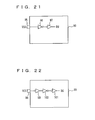
- FIG. 21 is a diagram showing the configuration according to a thirteenth embodiment of the invention.
- FIG. 22 is a diagram showing the configuration according to a fourteenth embodiment of the invention.
- FIG. 23 is a diagram schematically showing a whole configuration of a conventional semiconductor integrated circuit
- FIG. 24 is a diagram schematically showing the configuration of control signal generating circuitry in the semiconductor integrated circuit illustrated in FIG. 23;
- FIG. 25 is a diagram schematically showing signal waveforms at the time of a writing operation of the circuit illustrated in FIG. 24;
- FIG. 26 is a signal waveform chart showing an erasing operation of the circuit illustrated in FIG. 24;
- FIG. 27 is a diagram schematically showing the configuration of column selection signal generating circuitry in the semiconductor integrated circuit illustrated in FIG. 23;
- FIG. 28 is a timing chart representing operations of circuits illustrated in FIG. 27;
- FIG. 29 is a diagram showing the configuration of an input buffer circuit of the semiconductor integrated circuit illustrated in FIG. 23;
- FIG. 30 is a diagram showing the configuration of an output buffer circuit of the semiconductor integrated circuit illustrated in FIG. 23.
- FIGS. 31A and 31B are diagrams showing voltages applied to a nonvolatile memory cell at the time of writing/erasing data.
- FIG. 1 is a diagram schematically showing a whole configuration of a semiconductor integrated circuit according to the present invention.
- a semiconductor integrated circuit (semiconductor chip) 1 includes: an internal voltage generating circuit 2 for generating an internal voltage Vint from a high-level power supply voltage VCC and a low-level power supply voltage VSS that are applied to power supply pads 3 a and 3 b , respectively; an internal circuit 5 for performing a predetermined operation; a buffer circuit 6 coupled between the internal circuit 5 and a pad 7 ; and a switching circuit 10 for inactivating the buffer circuit 6 and transmitting the internal voltage Vint on an internal voltage transmission line 4 to the pad 7 when a test mode instruction signal (control signal) DU is activated.
- the pad 7 is coupled to an external pin terminal 8 via a bonding wire 9 after packaged.
- the internal circuit 5 includes an internal voltage using circuit 5 a which uses the internal voltage Vint on the internal voltage transmission line 4 and generates a signal/voltage having an amplitude of the internal voltage Vint level.
- the buffer circuit 6 is coupled to a predetermined signal processing circuit included in the internal circuit 5 . When the internal voltage using circuit 5 a performs an internal signal process operation, the buffer circuit 6 may be coupled to receive a signal from the internal voltage using circuit 5 a.
- the buffer circuit 6 In the semiconductor integrated circuit 1 , in a normal state, the buffer circuit 6 is coupled to the external pin terminal 8 via the pad 7 , buffers a signal for transference between the internal circuit 5 and the pad 7 . In a test operation mode, the switching circuit 10 is made active, the buffer circuit 6 is made inactive, and the internal voltage Vint on the internal voltage transmission line 4 is transmitted to the pad 7 . The pad 7 is therefore coupled to the external pin terminal 8 , and a tester can externally monitor the voltage level of the internal voltage Vint via the pin terminal 8 .
- the internal voltage Vint is one of the positive high voltage VPP, the negative high voltage VNN, and the reference voltage Vref.
- VPP positive high voltage
- VNN negative high voltage
- Vref reference voltage
- the internal voltage can be monitored without increasing the number of pins.
- the high-level power supply voltage VCC will be simply called a power supply voltage
- the low-level power supply voltage VSS will be called a ground voltage.
- FIG. 2 is a diagram schematically showing the configuration of an output section of the semiconductor memory device according to a first embodiment of the invention.
- the buffer circuit 6 is an output buffer circuit 6 A for buffering the internal read data bit intQ for outputting to a pad 7 a .
- the output buffer circuit 6 A includes: an inverter IVa which receives the internal read data bit intQ; an inverter IVb which receives a complementary output enable signal /OE of an inverted signal of the output signal OE; an inverter IVc which receives a test mode instruction signal (control signal) DU; an NAND circuit GTa for receiving output signals of the inverters IVb and IVc and the internal read data bit intQ; a three-input NOR circuit GTb for receiving the output of the inverter IVa, the output enable signal /OE, and the test mode instruction signal DU; a P-channel MOS transistor PQ 1 which is made conductive when an output signal of the NAND circuit GTa is at the L level and transmits the power supply voltage VCC to the pad 7 a ; and an N-channel MOS transistor NQ 1 which is made conductive when an output signal of the NOR circuit GTb is at the H level and transmits the ground voltage VSS to the pad 7 a.
- the switching circuit 10 includes a P-channel MOS transistor PQ 2 which is made conductive when the test mode instruction signal DU attains the high level and couples a reference voltage transmission line 4 a for transmitting the reference voltage Vref to the pad 7 a .
- the NAND circuit GTa and the NOR circuit GTb output an H-level signal and an L-level signal, respectively, and the output buffer circuit 6 A enters a disable state (inactive state).
- the switching circuit 10 includes the MOS transistor PQ 2 , a signal line for transmitting the control signal DU, and the inverter IVc.
- the reference voltage Vref from a Vref generating circuit 2 a for generating the reference voltage Vref is transmitted through the reference voltage transmission line 4 a .
- the reference voltage Vref has an intermediate voltage level between the levels of the power supply voltage VCC and the ground voltage VSS.
- test mode instruction signal DU When the test mode instruction signal DU is at the L level, the test mode instruction signal DU attains the H level of the power supply voltage VCC level, and the MOS transistor PQ 2 is turned off.
- the output enable signal /OE attains the L level
- the NAND circuit GTa and the NOR circuit GTb operate as an inverter and drive the MOS transistors PQ 1 and NQ 1 in accordance with the internal read data bit intQ.
- output enable signal /OE When the output enable signal /OE is at the H level, output signals of the NAND circuit GTa and the NOR circuit GTb are at the H level and the L level, respectively, and both the MOS transistors PQ 1 and NQ 1 enter an OFF state.
- the output signal of the inverter IVc attains the L level of the ground voltage VSS level.
- the MOS transistor PQ 2 is turned on and the reference voltage transmission line 4 a is coupled to the pad 7 a .
- the NAND circuit GTa and the NOR circuit GTb output H-level and L-level signals, respectively, and both the MOS transistors PQ 1 and NQ 1 are turned off.
- the reference voltage Vref generated by the Vref generating circuit 2 a is transmitted to the external pin terminal connected to the pad 7 a , and the voltage level of the reference voltage Vref can be monitored externally.
- the MOS transistor PQ 2 When the output buffer circuit 6 A is made inactive by the test mode instruction signal DU, the MOS transistor PQ 2 is turned on, and the reference voltage transmission line 4 a is connected to the pad 7 a , thereby enabling the reference voltage Vref to be accurately transmitted to the external pin terminal via the pad 7 a without being influenced by the output buffer circuit 6 A. Consequently, the reference voltage Vref can be monitored externally without increasing the number of pin terminals.
- FIG. 3 is a diagram showing the configuration of the output section of a semiconductor memory device according to a second embodiment of the invention.
- a P-channel MOS transistor PQ 3 is connected between a power supply node for supplying the power supply voltage VCC and the P-channel MOS transistor PQ 1 .
- the other configuration of the output buffer circuit 6 A is similar to that shown in FIG. 2 .
- the corresponding parts are denoted by the same reference numerals and their detailed description is omitted here.
- the switching circuit includes: a level shifting circuit 20 for converting the test mode instruction signal DU having the amplitude of the power supply voltage VCC level to a signal having the amplitude of the positive high voltage VPP level; a CMOS inverter 21 receiving the high voltage VPP as one of operation power supply voltages and inverting an output signal BDU of the level shifting circuit 20 ; and a P-channel MOS transistor PQ 2 for coupling a high voltage transmission line 4 b for transmitting the positive high voltage VPP to a pad 7 b in accordance with an output signal /BDU of the CMOS inverter 21 .
- the back gate and the source of the P-channel MOS transistor PQ 2 are connected together to the high voltage transmission line 4 b .
- the output signal BDU of the level shifting circuit 20 is applied to the gate of the MOS transistor PQ 3 .
- a VPP generating circuit 2 b is coupled to the high voltage transmission line 4 b and the positive high voltage VPP higher than the power supply voltage VCC is transmitted to the high voltage transmission line 4 b .
- the VPP generating circuit 2 b is made active when the writing/erasing command is applied in a manner similar to the conventional example and generates the high voltage VPP at a predetermined voltage level. The operations of the configuration shown in FIG. 3 will now be described.
- the output signal of the inverter IVc attains the H level, and the NAND circuit GTa and the NOR circuit GTb generate output signals in accordance with the internal read data bit intQ and the output enable signal /OE.
- the level shifting circuit 20 an output signal of the inverter IVc is at the H level (power supply voltage VCC level), the output signal BDU attains the low level, and the MOS transistor PQ 3 maintains the ON state.
- the output signal /BDU of the CMOS inverter 21 attains the H level of the high voltage VPP level, and the MOS transistor PQ 2 is turned off.
- both the MOS transistors PQ 1 and NQ 1 are turned off, and the output buffer circuit 6 A enters an output high impedance state.
- the NAND circuit GTa and the NOR circuit GTb each operate as an inverter, one of the MOS transistors PQ 1 and NQ 1 is turned on in accordance with the internal read data bit intQ, and a signal at the power supply voltage VCC level or a signal at the ground voltage level is transmitted to the pad 7 b.
- the MOS transistor PQ 2 In reading data, even when the VPP generating circuit 2 b stops the operation of generating the high voltage VPP and the voltage level of the high voltage VPP on the high voltage transmission line 4 b becomes equal to or lower than that of the power supply voltage VCC, since the back gate and the source of the MOS transistor PQ 2 are connected to the each other, the gate and source potentials thereof are equal to each other when the signal /BDU is at the H level. Therefore, irrespective of the voltage level of the pad 7 b , the MOS transistor PQ 2 normally maintains the OFF state.
- the MOS transistor PQ 2 is formed in an N well region independent of other MOS transistors.
- test mode instruction signal DU When the test mode instruction signal DU is set at the L level, the NAND circuit GTa and the NOR circuit GTb are made inactive and both the MOS transistors PQ 1 and NQ 1 are turned off.
- the output signal BDU from the level shifting circuit 20 attains the H level and the MOS transistor PQ 3 is turned off.
- the output signal /BDU of the CMOS inverter 21 attains the L level, the MOS transistor PQ 2 is turned on, and the high voltage transmission line 4 b is coupled to the pad 7 b .
- the source region in the MOS transistor PQ 1 is provided by a node receiving a high voltage
- the output signal of the NAND circuit GTa is at the power supply voltage VCC level
- the gate voltage of the MOS transistor PQ 1 is lower than the voltage of the pad 7 b . Consequently, the MOS transistor PQ 1 is turned on.
- the gate of the MOS transistor PQ 3 receives a signal at the high voltage VPP level. Even when the voltage level of the pad 7 b attains the high voltage VPP level, the MOS transistor PQ 3 is turned off. This is because when the back gate of the MOS transistor is not coupled to the source/drain, the node that receives a high voltage in the P-channel MOS transistor serves as a source. Consequently, even when the high voltage VPP is transmitted to the pad 7 b , it can be reliably prevented that a current flows from the high voltage transmission line 4 b to the node supplying the power supply voltage VCC.
- the voltage level of the high voltage VPP can be accurately monitored via the pin terminal connected to the pad 7 b without exerting an adverse influence on the internal circuit.
- the output buffer circuit is isolated from the power supply node supplying the power supply voltage VCC with the control signal of the high voltage level higher than that of the power supply voltage, and the high voltage transmission line is coupled to the pad. Even when the high voltage VPP is transmitted to the pad, it can be reliably prevented that a current flows in the power supply node, so that the high voltage VPP can be accurately monitored externally.
- FIG. 4 is a diagram showing the configuration of the output section of a semiconductor memory device according to a third embodiment of the invention.
- the switching circuit includes: a level shifting circuit 22 for inverting the logic level of the test mode instruction signal DU and converting the test mode instruction signal DU into a signal /LDU that changes between the power supply voltage VCC and the negative high voltage VNN; a CMOS inverter 23 receiving the output signal/LDU of the level shifting circuit 22 ; and an N-channel MOS transistor NQ 2 made conductive, when the output signal LDU of the CMOS inverter 23 is at the H level, to couple a pad 7 c and a negative voltage transmission line 4 c together.
- the back gate and the source of the MOS transistor NQ 2 are connected to the negative voltage transmission line 4 c .
- a VNN generating circuit 2 c for generating a negative high voltage VNN is coupled to the negative voltage transmission line 4 c .
- an N-channel MOS transistor NQ 3 which receives the output signal /LDU of the level shifting circuit 22 at its gate is connected between the N-channel MOS transistor NQ 1 at the output stage and the ground node.
- the other configuration of the output buffer circuit 6 A is similar to that shown in FIG. 2 .
- the corresponding parts are denoted by the same reference numerals and their detailed description is omitted here.
- the NAND circuit GTa and the NOR circuit GTb operate according to the output enable signal /OE and the internal read data bit intQ. Since the test mode instruction signal DU is at the L level, the level shifting circuit 22 sets the output signal /LDU at the H level of the power supply voltage VCC level.
- the MOS transistor NQ 3 is accordingly turned on and the source node of the MOS transistor NQ 1 is coupled to the ground node.
- the output signal LDU of the CMOS inverter 23 is at the negative voltage VNN level and the MOS transistor NS 2 is turned off.
- the gate of the MOS transistor NQ 2 receives the negative voltage VNN from the VNN generating circuit 2 c , so that the voltages at the gate, back gate, and source of the MOS transistor NQ 2 are the same and an OFF state of the MOS transistor NQ 2 is always maintained. Even if the VNN generating circuit 2 c stops the negative voltage generating operation and the voltage on the negative voltage transmission line 4 c attains the ground voltage level or higher, the voltage levels at the back gate, source, and gate of the MOS transistor NQ 2 are the same and the OFF state thereof is maintained. Thus, in the normal operation, the voltage VNN on the negative voltage transmission line 4 c can be prevented from exerting an adverse influence on the operation of the output buffer circuit 6 A.
- the test mode instruction signal DU attains the H level
- the NAND circuit GTa and the NOR circuit GTb output H-level and L-level signals, respectively, and the MOS transistors PQ 1 and NQ 1 are accordingly turned off.
- the output signal /LDU from the level shifting circuit 22 attains the voltage VNN level on the negative voltage transmission line 4 c .
- the MOS transistor NQ 3 is turned off.
- the output signal LDU of the CMOS inverter 23 attains the H level of the power supply voltage VCC level, the MOS transistor NQ 2 is turned on, and the negative voltage transmission line 4 c is coupled to the pad 7 c .
- the VNN generating circuit 2 c is made active by a command and generates the negative high voltage VNN at a predetermined voltage level, the negative high voltage VNN is transmitted to the pad 7 c via the MOS transistor NQ 2 , and the voltage level can be monitored externally.
- the MOS transistor NQ 1 receives a signal of the ground voltage level at its gate and is turned on.
- the MOS transistor NQ 3 receives the signal /LDU at the negative high voltage VNN level on its gate, and maintains the OFF state when the voltage level of the pad 7 c attains a level of the negative high voltage VNN. Consequently, it can be prevented that a current flows from the ground node to the negative high voltage VNN supply source, so that the voltage level of the negative high voltage VNN can be monitored externally.
- the MOS transistor NQ 2 is formed in an independent P-well and the source and the back gate thereof are connected to each other.
- the voltages at the control gate, back gate, and source region in the MOS transistor become the same, a depletion layer is spread toward the inside, and the flow of the current from the drain region to the source region is stopped. Irrespective of the voltage level of the pad 7 c relative to the voltage VNN on the negative voltage transmission line 4 c in the normal operation, the MOS transistor NQ 2 can be maintained in the OFF state.
- FIG. 5 is a diagram showing the configuration of the output section of a semiconductor memory device according to a fourth embodiment of the invention.
- the Vref 1 generating circuit 2 da to Vref 4 generating circuit 2 dd for generating four reference voltages Vref 1 to Vref 4 , respectively, are provided as an internal voltage generating circuit.
- Each of the reference voltages Vref 1 to Vref 4 is at the voltage level between the power supply voltage VCC and the ground voltage VSS, and the reference voltages Vref 1 to Vref 4 are transmitted on reference voltage transmission lines 4 da to 4 dd.
- a selection signal generating circuit 24 is provided, which is made active when the test mode instruction signal DU attains the H level, and which sequentially sets selection signals/Y 1 to /Y 4 from output nodes NY 1 to NY 4 to the L level of the selected state in accordance with a clock signal CLK.
- the selection signal generating circuit 24 is made inactive when the test mode instruction signal DU is at the L level, and sets all the selection signals /Y 1 to /Y 4 to the power supply voltage VCC level.
- the switching circuit further includes P-channel MOS transistors P 21 to P 24 which are selectively made conductive in response to the selection signals /Y 1 to /Y 4 from the selection signal generating circuit 24 and connect the reference voltage transmission lines 4 da to 4 dd to the pad 7 d .
- One of the selection signals /Y 1 to /Y 4 attains the L level (ground voltage level), one of the MOS transistors P 21 to P 24 is accordingly turned on, and one of the reference voltage transmission lines 4 da to 4 dd is connected to the pad 7 d.
- the configuration of the output buffer circuit 6 A is similar to that of FIG. 2 .
- the corresponding parts are designated by the same reference numerals, and the detailed description is omitted here.
- the output buffer circuit 6 A operates according to the output enable signal /OE and the internal read data bit intQ.
- test mode instruction signal DU is at the L level
- the selection signal generating circuit 24 is in an inactive state
- all the selection signals /Y 1 to /Y 4 are at the power supply voltage VCC level
- all the MOS transistors P 21 to P 24 maintain the off state. All the reference voltage transmission lines 4 da to 4 dd are therefore isolated from the pad 7 d.
- the output buffer circuit 6 A When the test mode instruction signal DU goes high to the H level, in a manner similar to the first to third embodiments, the output buffer circuit 6 A enters a high output impedance state.
- the selection signal generating circuit 24 performs, for example, a shifting operation in accordance with the clock signal CLK applied to the clock input CK to sequentially set the selection signals /Y 1 to /Y 4 to the L level of the selected state.
- the MOS transistors P 21 to P 24 are sequentially turned on and the reference voltage transmission lines 4 da to 4 dd are sequentially connected to the pad 7 d .
- the voltage level of each of the plurality of reference voltages Vref 1 to Vref 4 can be therefore monitored externally via the pad 7 d.
- the selection signal generating circuit 24 may be formed of, for example, a shift register which performs a shifting operation in accordance with the clock signal CLK. Although the generation of the clock signal CLK will be described in detail later, it is merely described here that the clock signal CLK is applied via an appropriate input pin terminal.
- FIG. 6 is a diagram showing an example of a specific configuration of the selection signal generating circuit 24 .
- the selection signal generating circuit 24 includes: a binary counter 24 a for performing a counting operation in response to the rising edge of the clock signal CLK applied to the clock input CK; an inverter 24 b receiving a complementary (inverted) test mode instruction signal /DU applied to the enable input EN; an inverter 24 c receiving a least significant count bit B 0 of the binary counter 24 a ; an inverter 24 d receiving an upper bit B 1 of the binary counter 24 a ; an NAND circuit 24 e receiving output signals of the inverters 24 b , 24 c , and 24 d and generating the selection signal /Y 1 at the node NY 1 ; an NAND circuit 24 f which receives the least significant count bit B 0 and output signals of the inverters 24 b and 24 d , and generates the selection signal/Y 2 at the node NY 2 ; an NAND circuit 24 g which
- the clock signal CLK is supplied in the test mode in the present embodiment, and is set at the L level in the normal mode of operation.
- the operations of the selection signal generating circuit shown in FIG. 6 will be described with reference to the signal waveform chart of FIG. 7 .
- the test mode instruction signal /DU is at the H level
- an output signal of the inverter 24 b is at the L level
- all the selection signals /Y 1 to /Y 4 are at the H level.
- the clock signal CLK is fixed at the L level and the binary counter 24 a does not perform the counting operation.
- the count bits B 0 and B 1 of the binary counter 24 a are reset to the initial value “00”.
- the test mode instruction signal /DU attains the L level
- an output signal of the inverter 24 b attains the H level
- the NAND circuits 24 e to 24 h enter an enabled state.
- Each of the count bits B 0 and B 1 of the binary counter 24 a is “0” and the selection signal /Y 1 attains the L level.
- the other selection signals /Y 2 to /Y 3 are set at the H level.
- the reference voltage Vref 1 is selected by the selection signal /Y 1 and transmitted to the pad 7 d .
- the clock signal CLK is applied.
- the binary counter 24 a performs the counting operation and the bit B 0 becomes “1”.
- the selection signal /Y 2 accordingly goes low to the L level and the selection signal /Y 1 attains the H level again.
- the other selection signals /Y 3 and /Y 4 maintain the H level.
- the binary counter 24 a performs the counting operation synchronously with the rising edge of the clock signal CLK, and the selection signals /Y 3 and /Y 4 are sequentially activated to the L level in accordance with the count bits B 0 and B 1 .
- the selection signals /Y 1 to /Y 4 can be sequentially made active synchronously with the clock signals CLK.
- FIG. 8 is a diagram schematically showing the configuration of a first modification of the fourth embodiment of the invention.
- a high voltage generating circuit 30 generates a plurality of high voltages VPP 1 to VPPM.
- the positive high voltages VPP 1 to VPPM may be generated from different high voltage generating circuits. These high voltages may be different in voltage level from each other or may include voltages of the same level if their applications are different.
- the positive high voltages VPP 1 to VPPM are at voltage levels higher than that of the power supply voltage VCC when generated.
- the selection signal generating circuit 24 for generating selection signals Y 1 to YM in accordance with the clock signal CLK and the test mode instruction signal /DU in order to select the high voltages VPP 1 to VPPM; a level shifting circuit 32 for shifting the selection signals Y 1 to YM to selection signals /Y 1 to /YM having amplitudes of the voltage levels of the corresponding high voltages VPP 1 to VPPM, respectively, and each inverted in logic level; and a selection circuit 33 for selecting one of the high voltages VPP 1 to VPPM in accordance with the selection signals /Y 1 to /YM from the level shifting circuit 32 and connecting the selected one to a pad 7 e.
- a level shifter 32 a receiving a selection signal Yi is shown as a representative.
- a P-channel MOS transistor 33 a for selecting a high voltage VPPi in accordance with the selection signal /Yi from the level shifter 32 a is shown as a representative.
- the P-channel MOS transistor 33 a has its back gate and source coupled to receive the high voltage VPPi.
- the P-channel MOS transistor PQ 3 is provided between the MOS transistor PQ 1 at the output stage and the power supply node.
- the configuration of the level shifting circuit 31 is similar to that of the level shifting circuit 20 shown in FIG. 3 .
- the configuration of the selection signal generating circuit 24 is similar to that of the selection signal generating circuit shown in FIG. 6 .
- the level shifter 32 a has the configuration similar to that of the level shifting circuit 20 shown in FIG. 3.
- a level shifter is provided for each of the selection signals Y 1 to YM.
- the P-channel MOS transistor for selecting a high voltage is provided for each of the selection signals /Y 1 to /YM.
- the signal BDU outputted from the level shifting circuit 31 is at the L level and the output buffer circuit 6 A outputs a signal to the pad 7 e in accordance with the internal signal.
- All the selection signals /Y 1 to /YM are at the H level.
- all the MOS transistors 33 a are in the OFF state and the high voltages VPP to VPPM are isolated from the pad 7 e.
- the selection signal generating circuit 24 sequentially sets the selection signals Y 1 to YM to the L level.
- the level shifting circuit 32 performs the level shifting in accordance with the selection signals Y 1 to YM, thereby generating the selection signals /Y 1 to /YM.
- the selection signal Yi attains the low level
- the MOS transistor 33 a is turned on, and the high voltage VPPi is transmitted to the pad 7 e .
- the output signal BDU of the level shifting circuit 31 is at the high voltage VPPmax level. Even when the high voltage VPPi is transmitted to the pad 7 e , the MOS transistor PQ 3 is reliably turned off, so that the voltage level of the high voltage VPPi can be accurately monitored externally via the pad 7 e.
- FIG. 9 is a diagram schematically showing the configuration of a second modification of the fourth embodiment of the invention.
- FIG. 9 shows the configuration of a portion of the level shifting circuit 31 for generating the signal BDU applied to the output buffer circuit 6 A.
- the other configuration is similar to that shown in FIG. 8 .
- P-channel MOS transistors PT 1 to PTM which receive he selection signals /Y 1 to /YM at their gates and a P-channel MOS transistor PTN which receives the test mode instruction signal DU at its gate are connected to a power supply node 31 a of the level shifting circuit 31 .
- MOS transistors PT 1 to PTM transmit the corresponding high voltages VPP 1 to VPPM to the power supply node 31 a when made conductive.
- MOS transistor PTN transmits the power supply voltage VCC to the power supply node 31 a when made conductive.
- the back gate and the source in each of the MOS transistors PT 1 to PTN are connected together to receive the high voltages VPP 1 to VPPM and the power supply voltage VCC, respectively. Therefore, irrespective of the voltage level of the power supply node 31 a , the voltage levels of the back gate, source, and control gate of each of the MOS transistors PT 1 to PTN become the same when not selected, and they maintain the OFF state irrespective of the voltage level of the power supply node 31 a when not selected.
- the signal BDU having an amplitude according to the selected high voltage is generated from the level shifting circuit 31 and is supplied to the control gate of the MOS transistor PQ 3 in the output buffer circuit 6 A shown in FIG. 6 .
- the MOS transistor PQ 3 can be reliably turned off and the voltage levels of the high voltages VPP 1 to VPPM can be accurately monitored externally.
- FIGS. 8 and 9 can be similarly applied for the negative high voltage VNN.
- a control signal having an amplitude of the negative high voltage level is supplied to a gate of an MOS transistor provided in series with the MOS transistor NQ 1 in the output buffer circuit 6 A in FIG. 8 .
- An N-channel MOS transistor is used in the selection circuit 33 .
- a plurality of internal voltages are selectively coupled to the pad, the output buffer circuit coupled to the pad is made inactive, and the voltage level of the pad is monitored externally.
- a plurality of internal voltages can be therefore monitored externally by using a reduced number of pin terminals.
- FIG. 10 is a diagram schematically showing the configuration of a fifth embodiment of the invention.
- the shift clock signal SC from the SC buffer 929 is supplied to the clock input CK in the selection signal generating circuit 24 that generates the selection signals /Y 1 to /Y 4 .
- the SC buffer 929 also applies the shift clock signal SC to the clock input CK of the Y address counter 912 shown in FIG. 23 .
- the shift clock signal SC is supplied from the pad 928 via the SC buffer 929 to the Y address counter 912 , thereby sequentially updating the Y address.
- the Y address counter 912 In monitoring the internal voltage, by generating the selection signals /Y 1 to /Y 4 in accordance with the shift clock signal SC from the SC buffer 929 , it is unnecessary to use the pin terminals for supplying a test-dedicated clock signal.
- the Y address counter 912 When writing, erasing, or reading is instructed by a command, the Y address counter 912 is made active under the control of the read/write/erase control circuit 913 shown in FIG. 23 . In this case, the voltage level of the internal voltage is simply monitored externally and it is unnecessary to select a column of memory cells in the memory array. While the test mode instruction signal DU is active, therefore, the Y address counter 912 may be held in an inactive state (reset state).
- the shift clock for column selection is used as a clock signal for performing the shifting operation for selecting an internal voltage. Consequently, it is unnecessary to use an extra pin terminal and to provide the pin terminal, the input buffer circuit and an input protection circuit for protecting the input buffer circuit, each dedicated to a test. The circuit occupying area is therefore reduced, and the reliability for the clock signal for a test is also guaranteed since a circuit which is used in the normal operation is employed.
- FIG. 11 is a diagram schematically showing the configuration of a sixth embodiment of the invention.
- lower address bits YAD ⁇ 0 > and YAD ⁇ 1 > from the Y address counter 912 are supplied to the selection signal generating circuit 35 .
- the selection signal generating circuit 35 corresponds to the configuration of the decoding section of the selection signal generating circuit 24 shown in FIG.
- the inverters 24 c and 24 d which receive the address bits YAD ⁇ 0 > and YAD ⁇ 1 >, respectively; the inverter 24 b which receives the test mode instruction signal /DU through the inverter IVc; and the NAND circuits 24 e to 24 h which enter an enable state when an output signal of the inverter 24 b is at the H level, to generate the selection signals /Y 1 to /Y 4 in accordance with the address bits YAD ⁇ 0 > and YAD ⁇ 1 > and complementary address bits /YAD ⁇ 0 > and /YAD ⁇ 1 > from the inverters 24 c and 24 d.
- the selection signal generating circuit 35 decodes the address bits YAD ⁇ 0 > and YAD ⁇ 1 > received from the Y address counter 912 and generates the selection signals /Y 1 to /Y 4 . It is unnecessary to provide a dedicated counting circuit (shift register), so that the circuit occupying area is reduced.
- Address bits YAD ⁇ 11 : 0 > from the Y address counter 912 are supplied to the Y decoder 905 .
- the Y decoder 905 performs a decoding operation to select a column in selecting a register circuit in the data register.
- the high voltages VPP and VNN are generated when selection of the data register is not performed.
- the decoding operation of the Y decoder 905 is stopped under the control of the control circuit 913 .
- the Y address counter 912 performs a counting operation in accordance with the shift clock signal SC from the SC buffer 929 .
- the count value of the Y address counter 912 is initially set to “0” in a test mode in monitoring the voltage level.
- the initial value of the Y address counter 912 is set to a Y address supplied externally when the counting operation of the Y address counter 912 is performed. In the operation mode of monitoring the internal voltage level externally, the count value of the Y address counter 912 is reset to the initial value, for example, in response to the activation of the test mode instruction signal DU.
- the Y address counter 912 may be constructed as in a serial EEPROM (Electrically Erasable Programmable ROM) in such a manner that a command, an X address and data are transferred via the same bus and the Y address is always started from the same count value of the Y address counter 912 .
- the internal operation When the level of a voltage generated internally is monitored externally, the internal operation may be performed. The internal operation may be also inhibited except the internal voltage generating operation.
- an internal voltage is selected with the lower bit of the Y address counter for column selection, so that the circuit occupying area is further reduced.
- FIG. 12 is a diagram schematically showing the configuration of a seventh embodiment of the invention.
- the buffer circuit 6 is an input buffer circuit 6 B, and the reference voltage Vref generated internally is transmitted to a pad 7 f connected to the input buffer circuit 6 B.
- the input buffer circuit 6 B includes: a P-channel MOS transistor PQ 4 and an N-channel MOS transistor NQ 4 receiving the signal Sig supplied to the pad 7 f at their respective gates; an N-channel MOS transistor NQ 5 for fixing an internal output node 44 to the ground voltage level when made conductive; and a P-channel MOS transistor PQ 5 connected between the P-channel MOS transistor PQ 4 and the power supply node.
- the switching circuit 10 includes: an OR circuit 41 which receives the test mode instruction signal DU and the chip select signal /CS and applies an output signal to the gates of the MOS transistors PQ 5 and NQ 5 ; an inverter 42 which inverts the test mode instruction signal DU; and a P-channel MOS transistor PQ 6 which is made conductive, when the output signal of the inverter 42 is at the L level, to couples the reference voltage transmission line 4 a to the pad 7 f .
- the reference voltage Vref is at the voltage level between the levels of the power supply voltage VCC and the ground voltage VSS.
- the OR circuit 41 and the inverter 42 receive the power supply voltage VCC as one operation power supply voltage.
- the reference voltage Vref is transmitted from the Vref generating circuit 2 a onto the reference voltage transmission line 4 a.
- the test mode instruction signal DU When the test mode instruction signal DU is at the L level, the output signal of the inverter 42 is at the H level, the MOS transistor PQ 6 is turned off, and the reference voltage transmission line 4 a and the pad 7 f are isolated from each other.
- the signal applied to the pad 7 f is at the power supply voltage VCC level and the MOS transistor PQ 6 maintains an OFF state (the MOS transistor PQ 6 is made conductive only when an overshoot occurs at the pad 7 f ). In such a state, the logic level of an output signal of the OR circuit 41 is determined according to the logic level of the chip select signal /CS.
- the MOS transistor PQ 5 When the chip select signal /CS is at the H level, the MOS transistor PQ 5 is turned off, the MOS transistor NQ 5 is turned on, the MOS transistor PQ 4 is isolated from the power supply node, and the internal signal IN of the internal node 44 is fixed at the ground voltage VSS level.
- the chip select signal /CS attains the L level, the MOS transistor PQ 5 is turned on and the MOS transistor NQ 5 is turned off.
- the MOS transistor PQ 4 is coupled to the power supply node, and the internal signal IN is generated according to the signal Sig applied to the pad 7 f.
- the output signal of the OR circuit 41 attains the H level.
- the input buffer circuit 6 B is held in an inactive state and the internal signal IN is fixed at the ground voltage VSS level.
- the MOS transistor PQ 6 is turned on and the reference voltage transmission line 4 a is coupled to the pad 7 f , thereby enabling the reference voltage Vref from the Vref generating circuit 2 a to be monitored via the pad 7 f .
- the reference voltage Vref is at the voltage level between the levels of the power supply voltage VCC and the ground voltage VSS, and both the MOS transistors PQ 4 and NQ 4 are turned on.
- the MOS transistor PQ 5 is, however, turned off by the signal at the H level of the power supply voltage VCC level from the OR circuit 41 , and generation of a through current in the input buffer circuit 6 B is prevented.
- the input buffer circuit 6 B is made inactive in the test mode and the reference voltage transmission line 4 a is connected to the input pad 7 f , thereby enabling the reference voltage Vref to be monitored externally via the pad and the external pin terminal connected to the input buffer circuit 6 b .
- the internal voltage can be monitored through the pin terminal used in the normal operation mode.
- FIG. 13 is a diagram showing the configuration of an eighth embodiment of the invention.
- the positive high voltage VPP from the VPP generating circuit 3 b is transmitted to an input pad 7 g .
- the positive high voltage VPP is at a voltage level higher than the power supply voltage VCC.
- a level shifting circuit 50 for converting the test mode instruction signal DU having an amplitude of the power supply voltage VCC level to a signal having an amplitude of the high voltage VPP level, in order to reliably turn off the MOS transistor PQ 6 for connecting the reference voltage transmission line 4 b and the input pad 7 g ; and a CMOS inverter circuit 51 for inverting an output signal of the level shifting circuit 50 .
- An output signal of the CMOS inverter circuit 51 is applied to the gate of the P-channel MOS transistor PQ 6 .
- the level shifting circuit 50 does not convert the logic level.
- the CMOS inverter circuit 51 receives the high voltage VPP as one operation power supply voltage.
- the configuration of the input buffer circuit 6 B is similar to that of the input buffer circuit shown in FIG. 12 and the corresponding parts are designated by the same reference numerals.
- the same operation as that shown in FIG. 12 is performed when the test mode instruction signal DU is at the L level.
- the input buffer circuit 6 B is selectively made active or inactive by the chip select signal /CS.
- the test most instruction signal DU is at the L level
- an output signal of the level shifting circuit 50 is similarly at the L level of the ground voltage level
- an output signal of the CMOS inverter 51 accordingly attains the high voltage VPP level
- the MOS transistor PQ 6 is set to an OFF state. Both the back gate and the source of the MOS transistor PQ 6 are connected to the high voltage transmission line 4 b .
- the MOS transistor PQ 6 is reliably fixed to the OFF state.
- the MOS transistor PQ 6 therefore, the high voltage transmission line 4 b and the input pad 7 g can be reliably isolated from each other irrespective of the voltage level of the signal Sig.
- the test mode instruction signal DU attains the H level
- the output signal of the OR circuit 41 attains the H level (power supply voltage VCC level)
- the MOS transistor PQ 5 is turned off.
- the MOS transistor NQ 5 is turned on and the input buffer circuit 6 B is made inactive.
- the output signal of the level shifting circuit 50 attains the high voltage VPP level on the high voltage transmission line 4 b
- the output signal of the CMOS inverter 51 accordingly attains the H level
- the MOS transistor PQ 6 is turned on. Consequently, the high voltage transmission line 4 b is coupled to the pad 7 g.
- the CMOS inverter 51 may not be particularly provided.
- a signal obtained by inverting the logic level of the test mode instruction signal DU may be directly outputted from the level shifting circuit 50 and applied to the gate of the MOS transistor PQ 6 .
- FIG. 14 is a diagram schematically showing the configuration of a modification of the eighth embodiment of the invention.
- the negative high voltage VNN is transmitted to an input pad 7 h .
- the input buffer circuit 6 B is coupled to the input pad 7 h .
- the configuration of the input buffer circuit 6 B is the same as that of the input buffer circuit 6 B shown in FIG. 13 . Therefore, the corresponding parts are designated by the same reference numerals and their detailed description is omitted here.
- a level shifting circuit 54 and the N-channel MOS transistor NQ 6 are provided.
- the level shifting circuit 54 converts the test mode instruction signal DU having the amplitude of the power supply voltage VCC level to a signal which changes between the power supply voltage VCC level and the negative high voltage VNN level.
- the N-channel MOS transistor NQ 6 selectively couples the input pad 7 h to the negative voltage transmission line 4 c in accordance with an output signal of the level shifting circuit 54 .
- the back gate and the source of the MOS transistor NQ 6 are connected to the negative voltage transmission line 4 c.
- a signal at the voltage VNN level on the negative transmission line 4 c is generated from the level shifting circuit 54 and is applied to the gate of the MOS transistor NQ 6 .
- the MOS transistor NQ 6 is responsively set in the OFF state irrespective of the voltage level of the signal Sig applied to the input pad 7 h . That is, the signal Sig changes between the ground voltage and the power supply voltage VCC, and the negative high voltage VNN is at the voltage level lower than the ground voltage when generated.
- the gate, source, and back gate of the MOS transistor NQ 6 are at the same voltage level, and the OFF state thereof can be reliably maintained.
- the input buffer circuit 6 B generates the internal signal IN in accordance with the signal Sig applied to the input pad 7 h without being influenced by the voltage level of the negative high voltage VNN on the negative voltage transmission line 4 c when the chip select signal /CS is at the L level.
- the input buffer circuit 6 B is made inactive.
- the level shifting circuit 54 receives the test mode instruction signal DU, generates a signal at the power supply voltage VCC level, and applies the generated signal to the gate of the MOS transistor NQ 6 .
- the MOS transistor NQ 6 is responsively turned on and the negative voltage transmission line 4 c is connected to the input pad 7 h .
- the MOS transistor PQ 4 is turned on.
- the MOS transistor PQ 5 is turned off in response to the output signal of the OR circuit 41 .
- the MOS transistor NQ 4 is in a deep OFF state by the negative high voltage VNN.
- the path of the through current in the input buffer circuit 6 B is reliably cut off.
- the voltage level of the negative high voltage VNN supplied from the VNN generating circuit 2 c to the negative voltage transmission line 4 c can be monitored externally via the input pad 7 h.
- the test mode instruction signal is level-shifted or converted, the high voltage transmission line is connected to the input pad, and the input buffer circuit is made inactive.
- the positive or negative high voltage can be therefore accurately monitored externally without exerting an adverse influence on the buffer circuit.
- the voltage level of the high voltage can be monitored externally with the pin terminal connected to the input buffer circuit.
- FIG. 15 is a diagram schematically showing the configuration of a ninth embodiment of the invention.
- a plurality of reference voltages Vref 1 to Vref 4 are selectively transmitted to an input pad 7 i . That is, the reference voltages Vref 1 to Vref 4 from Vref 1 generating circuit 2 da to Vref 4 generating circuit 2 dd are transmitted to the reference voltage transmission lines 4 da to 4 dd , respectively.
- a switching circuit for selecting the reference voltage includes: an inverter 55 which receives the test mode instruction signal DU; a selection signal generating circuit 56 which receives an output signal of the inverter 55 at an enable input EN, receives the clock signal CLK at a clock input CK, and performs a shifting operation (counting operation and decoding operation) to sequentially activate the column selection signals /Y 1 to /Y 4 to the L level; and P-channel MOS transistors P 61 to P 64 which are provided in correspondence to the selection signals /Y 1 to /Y 4 from the selection signal generating circuit 56 , respectively, and are made conductive, when the corresponding selection signals /Y 1 to /Y 4 are in an active state, to transmit the reference voltages Vref 1 to Vref 4 to the input pad 7 i.
- the input buffer circuit 6 B is made active or inactive according to an output signal of the OR circuit 41 that receives the test most instruction signal DU and the chip select signal /CS.
- the configuration of the input buffer circuit 6 B is similar to those of FIGS. 13 and 14, and the corresponding parts are designated by the same reference numerals and their detailed description is omitted here.
- the selection signal generating circuit 56 has the configuration similar to that of the selection signal generating circuit 24 shown in FIG. 5 . Alternately, any of the configurations shown in FIGS. 6, 10 , and 11 can be used therefor.
- the selection signal generating circuit 56 may simply be formed of a shift register for performing a shifting operation in accordance with the clock signal CLK.
- the input buffer circuit 6 B in the test operation mode, is held in an inactive state by the output signal of the OR circuit 41 .
- the selection signal generating circuit 56 receives the signal at the L level at the enable input EN and is made active to sequentially activate the column selection signals /Y 1 to /Y 4 in accordance with the clock signal CLK. Any one of the MOS transistors P 61 to P 64 is made conductive, and any one of the reference voltages Vref 1 to Vref 4 is transmitted to the input pad 7 i .
- Each of the reference voltages Vref 1 to Vref 4 is at a voltage level between the power supply voltage VCC and the ground voltage VSS, and the MOS transistor PQ 5 is in an OFF state in the input buffer circuit 6 B, so that the path of a through current in the input buffer circuit 6 B is reliably cut off.
- the output signal of the inverter 55 is at the H level, all the selection signals /Y 1 to /Y 4 from the selection signal generating circuit 56 attain the H level of the power supply voltage VCC level, and all the MOS transistors P 61 to P 64 are turned off. Consequently, the reference voltage transmission lines 4 da to 4 dd are reliably isolated from the input pad 7 i , and the voltages Vref 1 to Vref 4 are reliably prevented from exerting an adverse influence on the input buffer circuit 6 B.
- FIG. 16 is a diagram showing the configuration of a modification of the ninth embodiment of the invention.
- a high voltage generating circuit 60 generates a plurality of negative high voltages VNN 1 to VNN 4 onto negative voltage transmission lines 4 ca to 4 cd , respectively.
- a switching circuit for selecting one of the negative high voltages VNN 1 to VNN 4 includes: a selection signal generating circuit 62 which is made active in response to the activation of the test mode instruction signal DU and generates a selection signal by performing a shifting operation (counting operation and decoding operation) synchronously with the clock signal CLK; a level shifting circuit 64 for shifting the level of a selection signal from the selection signal generating circuit 62 ; and a selection circuit 66 for connecting one of the negative voltage transmission lines 4 ca to 4 cd to the input pad 7 j in accordance with the signals Y 1 to Y 4 from the level shifting circuit 64 .
- the level shifting circuit 64 includes level shifters 64 a to 64 d provided in correspondence with the selection signals Y 1 to Y 4 , respectively.
- the level shifters 64 a to 64 d receive the corresponding negative high voltages VNN 1 to VNN 4 as one operation power supply voltage and receive the power supply voltage VCC as the other operation power supply voltage.
- the selection signal generating circuit 62 generates a selection signal having the amplitude VCC.
- the selection signals Y 1 to Y 4 which change between the corresponding negative high voltages VNN 1 to VNN 4 and the power supply voltage VCC are generated by the level shifters 64 a to 64 d.
- the input buffer circuit 6 B has the configuration as that shown in FIG. 15, the corresponding parts are designated by the same reference numerals, and their detailed description is omitted here.
- the back gate and the source in each of N-channel MOS transistors N 61 to N 64 included in the selection circuit 66 are connected together. Even when any of the negative high voltages VNN 1 to VNN 4 is selected and coupled to the input pad 7 j , the MOS transistors N 61 to N 64 which are not selected have same voltage level at the control gate, back gate, and source, and normally maintain an OFF state. A negative high voltage can be transmitted to the input pad 7 j and monitored externally.
- the selecting operation can be similarly performed with respect to the positive high voltages VPP 1 to VPP 4 .
- one of a plurality of internal voltages is selected and transmitted to the input pad.
- a plurality of internal voltages can be therefore monitored externally via one existing input pin terminal.
- FIG. 17 is a diagram showing the configuration of a tenth embodiment of the invention.
- the reference voltage transmission line 4 a for transmitting a reference voltage from the Vref generating circuit 2 a that generates the reference voltage Vref is provided with: a transmission gate TG 1 which is conductive, when the test mode instruction signal DU is at the L level, to transmit the reference voltage from the Vref generating circuit 2 a ; and a transmission gate TG 2 which is conductive, when the test mode instruction signal DU is at the H level, to connect a reference voltage line 4 ab for transmitting an internal reference voltage intVref to a pad 7 k .
- the reference voltage transmission line 4 a is divided into two reference voltage lines 4 aa and 4 ab .
- the configuration of the input buffer circuit 6 B is similar to any of those shown in FIGS. 12 to 16 , the corresponding parts are designated by the same reference numerals, and their detailed description is omitted here.
- the transmission gate TG 1 is made nonconductive and the transmission stage TG 2 is made conductive.
- the Vref generating circuit 2 a is responsively isolated from the reference voltage line 4 ab .
- the reference voltage line 4 ab is connected to the input pad 7 k .
- a voltage is applied externally to the input pad 7 k , and the voltage level of the internal reference voltage intVref is forcedly set externally.
- the voltage level of the reference voltage intVref determines the voltage levels of the high voltages VPP and VNN that are generated internally.
- the MOS transistor PQ 5 When the voltage externally applied to the input pad 7 k is at an intermediate voltage level, the MOS transistor PQ 5 is turned off in the test mode, and a through current flowing path in the input buffer circuit 6 B is cut off.
- the internal reference voltage intVref is set to a voltage level which is either higher than that of the power supply voltage VCC or lower than the ground voltage VSS, one of the MOS transistors PQ 4 and NQ 4 is turned off. Similarly, a path through which a through current flows in the input buffer circuit 6 B is cut off.
- the voltage levels of the negative high voltage VNN and the positive high voltage VPP can be set externally.
- the internal voltage can be set at a desired voltage level with the input pin terminal, and estimation of the internal circuit and an acceleration test such as a burn-in test can be carried out without increasing the number of pins.
- FIG. 18 is a diagram schematically showing the configuration of an eleventh embodiment of the invention.
- a command decoder 70 performs a decoding operation in accordance with signals and data received from a DIN buffer 911 a , a WE buffer 923 , and an RES buffer 925 and activates a test mode signal ⁇ DU. That is, a new command for externally monitoring the internal voltage or forcedly setting the internal voltage is generated.
- the test mode instruction signal DU is generated by a set/reset flip-flop 74 which is set in response to the activation (H level) of the test mode signal ⁇ DU and is reset in response to a system reset signal RES applied from the RES buffer 925 via an inverter.
- the reset signal RES is at the H level in an inactive state.
- the set/reset flip-flop 74 is responsively set, and the test mode instruction signal DU attains an active state of the H level. In such a state, a necessary number of commands for generating an internal voltage or internal voltages are applied externally. A command only for generating an internal voltage, but for causing no internal write/erase/read operation may be newly prepared. A read/write/erase command may be used as a command for generating an internal voltage.
- the input buffer circuit it is necessary to receive a command and activate the chip select signal /CS.
- a pad coupled to the input buffer circuit In the case of coupling a pad coupled to the input buffer circuit to the internal voltage line, it is necessary to set a pad for monitoring/forcedly setting an internal voltage as an input pad which is not used at the time of applying an internal voltage generating command.
- An example of such a pad is the shift clock input terminal SC (except the case of selecting one of a plurality of reference voltages and internal voltages). Alternatively, a specific address pin terminal may be used.
- a command “33h” instructing a test mode is applied to the DIN buffer 911 a .
- the write enable signal WE is set to the L level.
- the command decoder 70 performs a decoding operation, detects designation of the test mode of monitoring/forcedly setting an internal voltage, and activates the test mode signal ⁇ DU.
- the test mode signal ⁇ DU is made active, the set/reset flip-flop 74 is set, and the test mode instruction signal DU is made active.
- the command decoder 70 drives the test mode signal ⁇ DU into an inactive state.
- the set/reset flip-flop 74 maintains the set state and the test mode instruction signal DU maintains the H level, a test mode entry period is completed.
- the internal voltage generation commands are sequentially applied via the data input terminal group 917 .
- the command decoder 70 decodes the internal voltage generation command and applies an internal voltage generation instruction signal to the write/read/erase control circuit 913 .
- the reference voltage Vref, positive high voltage VPP, or negative high voltage VNN is generated.
- the internal voltage generated is monitored externally or forcedly set from an outside of the memory device by any of the methods described in the foregoing first to tenth embodiments.
- the internal voltage generation command may be a command instructing the writing/reading/erasing operation, and the write/read/erase control circuit 913 executes a necessary operation according to the designated operation.
- the reset signal RES is set to the L level
- the reset/reset flip-flop 74 is reset
- the test mode instruction signal DU is driven to the L level.
- a test mode can be set without requiring a new pin terminal.
- FIG. 20 is a diagram schematically showing the configuration of a twelfth embodiment of the invention.
- inverters 92 and 93 of two stages are connected to an external pin terminal 91 which is set in an open state (no connection (NC) state) in a practical use.
- the test mode instruction signal DU is generated from the inverter 93 .
- the input of the inverter 92 is connected to the external pin terminal 91 and a pull-down resistor 94 having a large resistance value RPULL is connected.
- the external pin terminal 91 is made open.
- the test mode instruction signal DU is held at the L level by the pull-down resistor 94 .
- the external pin terminal 91 is set to the power supply voltage VCC level. Accordingly, the test mode instruction signal DU attains the H level.
- the external pin terminal 91 is supplied with the power supply voltage VCC only in a test, and in a practical use, is kept in an open state, so that no problem occurs.
- FIG. 21 is a diagram schematically showing the configuration of a thirteenth embodiment of the invention.
- an external pin terminal 95 of a semiconductor integrated circuit device 90 is fixed to the ground voltage VSS in a practical use.
- Inverters 96 and 97 of two stages are connected to the external pin terminal 95 .
- the test mode instruction signal DU is generated from the inverter 97 at the output stage.
- the external pin terminal 95 is connected to, for examples a shielding wire.
- the power supply voltage VCC is applied to the external pin terminal 95 .
- the test mode instruction signal DU attains the H level and a test on an internal voltage can be performed. Even when a pin terminal used for a shielding wire for canceling noises internally, or the like, is fixed to the power supply voltage VCC level in a test mode, the shielding effect does not deteriorate. Without causing an erroneous operation in the internal circuit, the test mode instruction signal DU can be easily generated without providing an additional pin terminal.
- FIG. 22 is a diagram schematically showing the configuration of a fourteenth embodiment of the invention.
- an external pin terminal 98 of the semiconductor integrated circuit device 90 is fixed at the power supply voltage VCC level in a normal practical use.
- Inverters 99 to 101 of odd-number stages (three stages) are connected in series to the external pin terminal 98 .
- the test mode instruction signal DU is generated from the inverter 101 at the final stage.
- the external pin terminal 98 is connected to, for example, a shielding wire internally. In a test on an internal voltage, the external pin terminal 98 is set at the ground voltage VSS.
- the test mode instruction signal DU can be accordingly set to the H level.
- test mode instruction signal can be applied.
- the data output buffer circuit which operates in response to the output enable signal /OE is described.
- a pin terminal for externally outputting a ready/busy signal instructing a waiting of an access when the writing or erasing operation is performed internally is provided.
- an output buffer circuit therefore, an output buffer circuit which outputs a ready/busy signal may be employed.
- a nonvolatile semiconductor memory device As an example of a semiconductor integrated circuit, a nonvolatile semiconductor memory device is described.
- the present invention can be also applied to a memory such as a dynamic random access memory (DRAM), in which a plurality of voltages, such as a high voltage VPP applied to a selected word line, a negative bias voltage VNN applied to the substrate region, and the reference voltage Vref at an intermediate voltage level used for, for example, precharging a bit line are generated.
- DRAM dynamic random access memory
- the semiconductor integrated circuit is not generally limited to a memory.
- the invention can be applied to a semiconductor circuit device including a circuit in which an internal voltage different in voltage level from a power supply voltage and a ground voltage, which are externally applied, is generated.
- a voltage generated internally is coupled to a pad connected to an external pin terminal and a corresponding buffer circuit is made inactive. Therefore, it is unnecessary to newly provide a pin terminal, the internal voltage can be monitored or forcedly applied from an outside of the device of interest, and an internal circuit can be measured and estimated even after packaging. When a failure occurs after packaging, the cause of a failure can be efficiently analyzed.
Landscapes
- Engineering & Computer Science (AREA)
- Theoretical Computer Science (AREA)
- Physics & Mathematics (AREA)
- General Engineering & Computer Science (AREA)
- General Physics & Mathematics (AREA)
- Dram (AREA)
- Read Only Memory (AREA)
- For Increasing The Reliability Of Semiconductor Memories (AREA)
- Tests Of Electronic Circuits (AREA)
Abstract
Description
Claims (26)
Applications Claiming Priority (3)
| Application Number | Priority Date | Filing Date | Title |
|---|---|---|---|
| JP2000-255545 | 2000-08-25 | ||
| JP2000-255545(P) | 2000-08-25 | ||
| JP2000255545A JP2002074996A (en) | 2000-08-25 | 2000-08-25 | Semiconductor integrated circuit |
Publications (2)
| Publication Number | Publication Date |
|---|---|
| US20020024330A1 US20020024330A1 (en) | 2002-02-28 |
| US6549480B2 true US6549480B2 (en) | 2003-04-15 |
Family
ID=18744315
Family Applications (1)
| Application Number | Title | Priority Date | Filing Date |
|---|---|---|---|
| US09/774,719 Expired - Lifetime US6549480B2 (en) | 2000-08-25 | 2001-02-01 | Semiconductor integrated circuit allowing internal voltage to be measured and controlled externally |
Country Status (2)
| Country | Link |
|---|---|
| US (1) | US6549480B2 (en) |
| JP (1) | JP2002074996A (en) |
Cited By (31)
| Publication number | Priority date | Publication date | Assignee | Title |
|---|---|---|---|---|
| US20030042485A1 (en) * | 2001-09-03 | 2003-03-06 | Mitsubishi Denki Kabushiki Kaisha | Semiconductor integrated circuit device capable of tuning of internal power supply voltages generated by a plurality of internal power generating circuits |
| US20030140295A1 (en) * | 2002-01-18 | 2003-07-24 | Antley Richard L. | Integrated circuit having electrically isolatable test circuitry |
| US20030151967A1 (en) * | 2002-02-14 | 2003-08-14 | Wataru Nagai | Dram power-source controller |
| US20040057289A1 (en) * | 2002-09-25 | 2004-03-25 | Infineon Technologies North America Corp. | System and method for monitoring internal voltages on an integrated circuit |
| US20040109368A1 (en) * | 2002-12-03 | 2004-06-10 | Matsushita Electric Industrial Co., Ltd. | Semiconductor integrated circuit device |
| US20040190348A1 (en) * | 2002-11-18 | 2004-09-30 | Micron Technology, Inc. | Automatic reference voltage regulation in a memory device |
| US20040208077A1 (en) * | 2003-04-16 | 2004-10-21 | Samsung Electronics Co., Ltd. | Semiconductor memory device and layout method thereof |
| US6809970B2 (en) * | 2001-08-30 | 2004-10-26 | Micron Technology, Inc. | Input stage apparatus and method having a variable reference voltage |
| US20040222812A1 (en) * | 2003-03-21 | 2004-11-11 | Gerd Frankowsky | Integrated circuit having a test circuit |
| US20050068817A1 (en) * | 2003-09-30 | 2005-03-31 | Reidar Lindstedt | Circuit arrangement for setting a voltage supply for a test mode of an integrated memory |
| US20050184771A1 (en) * | 2003-12-26 | 2005-08-25 | Kiyotaka Uchigane | Semiconductor apparatus |
| US20050210175A1 (en) * | 2004-03-08 | 2005-09-22 | Jung-Bae Lee | Memory module capable of improving the integrity of signals transmitted through a data bus and a command/address bus, and a memory system including the same |
| US20050229050A1 (en) * | 2004-04-07 | 2005-10-13 | Kabushiki Kaisha Toshiba | Semiconductor device |
| US20050243616A1 (en) * | 2004-04-28 | 2005-11-03 | Matsushita Electric Industrial Co., Ltd. | Non-volatile semiconductor storage device |
| US20060007753A1 (en) * | 2004-07-08 | 2006-01-12 | Jong-Hyun Choi | Isolation control circuit and method for a memory device |
| US20060012400A1 (en) * | 2004-07-14 | 2006-01-19 | Nec Electronics Corporation | Electric potential switching circuit, flash memory with electric potential switching circuit, and method of switching electric potential |
| US20060104134A1 (en) * | 2004-10-04 | 2006-05-18 | Dong-Jun Kim | Semiconductor memory devices incorporating voltage level shifters for controlling a VPP voltage level independently and methods of operating the same |
| US20060179378A1 (en) * | 2005-01-27 | 2006-08-10 | Matsushita Electric Industrial Co., Ltd. | Semiconductor integrated circuit and method of testing the same |
| US20070070741A1 (en) * | 2005-09-29 | 2007-03-29 | Hynix Semiconductor Inc. | Semiconductor memory device for measuring internal voltage |
| US7221170B2 (en) | 2005-02-01 | 2007-05-22 | Samsung Electronics Co., Ltd. | Semiconductor test circuit |
| US20070253125A1 (en) * | 2006-04-27 | 2007-11-01 | Naoki Kuroda | Semiconductor integrated circuit |
| US20070285994A1 (en) * | 2006-04-27 | 2007-12-13 | Oki Electric Industry Co., Ltd. | Semiconductor memory device |
| US20090003088A1 (en) * | 2007-06-27 | 2009-01-01 | Hynix Semiconductor Inc. | Semiconductor memory device |
| US20090303802A1 (en) * | 2004-12-30 | 2009-12-10 | Samsung Electronics Co., Ltd. | Semiconductor memory module and semiconductor memory system having termination resistor units |
| US20100090675A1 (en) * | 2008-10-10 | 2010-04-15 | Elpida Memory, Inc. | Semiconductor device and test method therefor |
| US20100118639A1 (en) * | 2008-11-13 | 2010-05-13 | Hynix Semiconductor Inc. | Semiconductor memory apparatus |
| US20100226185A1 (en) * | 2004-12-30 | 2010-09-09 | Samsung Electronics Co., Ltd. | Semiconductor memory module and semiconductor memory system having termination resistor units |
| US20110188325A1 (en) * | 2010-02-02 | 2011-08-04 | Elpida Memory, Inc. | Semiconductor device and data processing system |
| CN101246384B (en) * | 2007-02-12 | 2012-05-23 | 瑞昱半导体股份有限公司 | Configuration initialization circuit and method thereof |
| US8792274B1 (en) * | 2007-10-01 | 2014-07-29 | Marvell International Ltd. | Multi-level memory cell read, program, and erase techniques |
| TWI473115B (en) * | 2008-01-10 | 2015-02-11 | Winbond Electronics Corp | Memory and voltage monitor device thereof |
Families Citing this family (12)
| Publication number | Priority date | Publication date | Assignee | Title |
|---|---|---|---|---|
| US6515934B2 (en) * | 1999-07-26 | 2003-02-04 | Mitsubishi Denki Kabushiki Kaisha | Semiconductor device including internal potential generating circuit allowing tuning in short period of time and reduction of chip area |
| US7584315B2 (en) | 2003-04-10 | 2009-09-01 | Panasonic Corporation | Integrated circuit monitoring an internal signal converted from an analog input signal |
| JP4510498B2 (en) * | 2004-04-05 | 2010-07-21 | セイコーインスツル株式会社 | Semiconductor integrated circuit |
| CA2541046A1 (en) * | 2006-03-27 | 2007-09-27 | Mosaid Technologies Incorporated | Power supply testing architecture |
| JP2007278987A (en) * | 2006-04-11 | 2007-10-25 | Ricoh Co Ltd | Semiconductor testing device |
| JP2008123642A (en) * | 2006-11-15 | 2008-05-29 | Samsung Electronics Co Ltd | Control circuit of negative potential monitor pad and nonvolatile memory equipped therewith |
| KR100784865B1 (en) * | 2006-12-12 | 2007-12-14 | 삼성전자주식회사 | Nand flash memory device and memory system including the same |
| JP5182011B2 (en) * | 2008-10-27 | 2013-04-10 | 富士通セミコンダクター株式会社 | Semiconductor device and test method of semiconductor device |
| JP5932324B2 (en) * | 2011-12-21 | 2016-06-08 | ピーエスフォー ルクスコ エスエイアールエルPS4 Luxco S.a.r.l. | Semiconductor device and test method thereof |
| JP6020076B2 (en) * | 2012-11-16 | 2016-11-02 | 株式会社ソシオネクスト | Interface circuit and semiconductor device |
| JP6170596B1 (en) * | 2016-06-15 | 2017-07-26 | ウィンボンド エレクトロニクス コーポレーション | Semiconductor device |
| KR20180051984A (en) * | 2016-11-09 | 2018-05-17 | 에스케이하이닉스 주식회사 | Semiconductor memory device and operating method thereof |
Citations (5)
| Publication number | Priority date | Publication date | Assignee | Title |
|---|---|---|---|---|
| JPH0720209A (en) | 1993-07-05 | 1995-01-24 | Fujitsu Ltd | Integrated circuit with feedthrough current prevention function |
| US5426616A (en) * | 1990-05-21 | 1995-06-20 | Hitachi, Ltd. | Semiconductor IC device having a voltage conversion circuit which generates an internal supply voltage having value compensated for external supply voltage variations |
| US5557571A (en) * | 1994-11-29 | 1996-09-17 | Mitsubishi Denki Kabushiki Kaisha | Dynamic random access memory with internal testing switches |
| JPH1173800A (en) | 1997-08-28 | 1999-03-16 | Nec Corp | Semiconductor device and its testing method |
| US6339357B1 (en) * | 1997-08-12 | 2002-01-15 | Mitsubishi Denki Kabushiki Kaisha | Semiconductor integrated circuit device capable of externally monitoring internal voltage |
-
2000
- 2000-08-25 JP JP2000255545A patent/JP2002074996A/en not_active Withdrawn
-
2001
- 2001-02-01 US US09/774,719 patent/US6549480B2/en not_active Expired - Lifetime
Patent Citations (6)
| Publication number | Priority date | Publication date | Assignee | Title |
|---|---|---|---|---|
| US5426616A (en) * | 1990-05-21 | 1995-06-20 | Hitachi, Ltd. | Semiconductor IC device having a voltage conversion circuit which generates an internal supply voltage having value compensated for external supply voltage variations |
| JPH0720209A (en) | 1993-07-05 | 1995-01-24 | Fujitsu Ltd | Integrated circuit with feedthrough current prevention function |
| US5557571A (en) * | 1994-11-29 | 1996-09-17 | Mitsubishi Denki Kabushiki Kaisha | Dynamic random access memory with internal testing switches |
| US6339357B1 (en) * | 1997-08-12 | 2002-01-15 | Mitsubishi Denki Kabushiki Kaisha | Semiconductor integrated circuit device capable of externally monitoring internal voltage |
| JPH1173800A (en) | 1997-08-28 | 1999-03-16 | Nec Corp | Semiconductor device and its testing method |
| US5942808A (en) * | 1997-08-28 | 1999-08-24 | Nec Corporation | Semiconductor device with plural power supply circuits, plural internal circuits, and single external terminal |
Cited By (63)
| Publication number | Priority date | Publication date | Assignee | Title |
|---|---|---|---|---|
| US6809970B2 (en) * | 2001-08-30 | 2004-10-26 | Micron Technology, Inc. | Input stage apparatus and method having a variable reference voltage |
| US6928010B2 (en) * | 2001-09-03 | 2005-08-09 | Renesas Technology Corp. | Semiconductor integrated circuit device capable of tuning of internal power supply voltages generated by a plurality of internal power generating circuits |
| US20030042485A1 (en) * | 2001-09-03 | 2003-03-06 | Mitsubishi Denki Kabushiki Kaisha | Semiconductor integrated circuit device capable of tuning of internal power supply voltages generated by a plurality of internal power generating circuits |
| US20080276145A1 (en) * | 2002-01-18 | 2008-11-06 | Texas Instruments Incorporated | Integrated circuit having electrically isolatable test circuitry |
| US7823038B2 (en) * | 2002-01-18 | 2010-10-26 | Texas Instruments Incorporated | Connecting analog response to separate strobed comparator input on IC |
| US7124341B2 (en) * | 2002-01-18 | 2006-10-17 | Texas Instruments Incorporated | Integrated circuit having electrically isolatable test circuitry |
| US20070035324A1 (en) * | 2002-01-18 | 2007-02-15 | Texas Instruments Incorporated | Integrated circuit having electrically isolatable test circuitry |
| US7418643B2 (en) * | 2002-01-18 | 2008-08-26 | Texas Instruments Incorporated | Integrated circuit having electrically isolatable test circuitry |
| US20090284267A1 (en) * | 2002-01-18 | 2009-11-19 | Texas Instruments Incorporated | Integrated circuit having electrically isolatable test circuitry |
| US20030140295A1 (en) * | 2002-01-18 | 2003-07-24 | Antley Richard L. | Integrated circuit having electrically isolatable test circuitry |
| US7587648B2 (en) * | 2002-01-18 | 2009-09-08 | Texas Instruments Incorporated | Integrated circuit having electrically isolatable test circuitry |
| US6791894B2 (en) * | 2002-02-14 | 2004-09-14 | Oki Electric Industry Co., Ltd. | DRAM power-source controller that reduces current consumption during standby |
| US20030151967A1 (en) * | 2002-02-14 | 2003-08-14 | Wataru Nagai | Dram power-source controller |
| US20040057289A1 (en) * | 2002-09-25 | 2004-03-25 | Infineon Technologies North America Corp. | System and method for monitoring internal voltages on an integrated circuit |
| US6845048B2 (en) * | 2002-09-25 | 2005-01-18 | Infineon Technologies Ag | System and method for monitoring internal voltages on an integrated circuit |
| US20040190348A1 (en) * | 2002-11-18 | 2004-09-30 | Micron Technology, Inc. | Automatic reference voltage regulation in a memory device |
| US6842385B2 (en) * | 2002-11-18 | 2005-01-11 | Micron Technology, Inc. | Automatic reference voltage regulation in a memory device |
| US20040109368A1 (en) * | 2002-12-03 | 2004-06-10 | Matsushita Electric Industrial Co., Ltd. | Semiconductor integrated circuit device |
| US7102413B2 (en) | 2002-12-03 | 2006-09-05 | Matsushita Electric Industrial Co., Ltd. | Semiconductor integrated circuit device |
| US20040222812A1 (en) * | 2003-03-21 | 2004-11-11 | Gerd Frankowsky | Integrated circuit having a test circuit |
| US20040208077A1 (en) * | 2003-04-16 | 2004-10-21 | Samsung Electronics Co., Ltd. | Semiconductor memory device and layout method thereof |
| US7075849B2 (en) * | 2003-04-16 | 2006-07-11 | Samsung Electronics Co., Ltd. | Semiconductor memory device and layout method thereof |
| US6950358B2 (en) * | 2003-09-30 | 2005-09-27 | Infineon Technologies, Ag | Circuit arrangement for setting a voltage supply for a test mode of an integrated memory |
| US20050068817A1 (en) * | 2003-09-30 | 2005-03-31 | Reidar Lindstedt | Circuit arrangement for setting a voltage supply for a test mode of an integrated memory |
| US20050184771A1 (en) * | 2003-12-26 | 2005-08-25 | Kiyotaka Uchigane | Semiconductor apparatus |
| US20100191880A1 (en) * | 2004-03-08 | 2010-07-29 | Samsung Electronics Co., Ltd. | Memory module capable of improving the integrity of signals transmitted through a data bus and a command/address bus, and a memory system including the same |
| US8117363B2 (en) * | 2004-03-08 | 2012-02-14 | Samsung Electronics Co., Ltd. | Memory module capable of improving the integrity of signals transmitted through a data bus and a command/address bus, and a memory system including the same |
| US7716401B2 (en) * | 2004-03-08 | 2010-05-11 | Samsung Electronics Co., Ltd. | Memory module capable of improving the integrity of signals transmitted through a data bus and a command/address bus, and a memory system including the same |
| US20050210175A1 (en) * | 2004-03-08 | 2005-09-22 | Jung-Bae Lee | Memory module capable of improving the integrity of signals transmitted through a data bus and a command/address bus, and a memory system including the same |
| US20050229050A1 (en) * | 2004-04-07 | 2005-10-13 | Kabushiki Kaisha Toshiba | Semiconductor device |
| US20050243616A1 (en) * | 2004-04-28 | 2005-11-03 | Matsushita Electric Industrial Co., Ltd. | Non-volatile semiconductor storage device |
| US7310277B2 (en) * | 2004-04-28 | 2007-12-18 | Matsushita Electric Industrial Co., Ltd. | Non-volatile semiconductor storage device with specific command enable/disable control signal |
| US20060007753A1 (en) * | 2004-07-08 | 2006-01-12 | Jong-Hyun Choi | Isolation control circuit and method for a memory device |
| US7298655B2 (en) * | 2004-07-08 | 2007-11-20 | Samsung Electronics Co., Ltd. | Isolation control circuit and method for a memory device |
| US20060012400A1 (en) * | 2004-07-14 | 2006-01-19 | Nec Electronics Corporation | Electric potential switching circuit, flash memory with electric potential switching circuit, and method of switching electric potential |
| US7327615B2 (en) * | 2004-07-14 | 2008-02-05 | Nec Electronics Corporation | Electric potential switching circuit, flash memory with electric potential switching circuit, and method of switching electric potential |
| US7289380B2 (en) * | 2004-10-04 | 2007-10-30 | Samsung Electronics Co., Ltd. | Semiconductor memory devices incorporating voltage level shifters for controlling a VPP voltage level independently and methods of operating the same |
| US20060104134A1 (en) * | 2004-10-04 | 2006-05-18 | Dong-Jun Kim | Semiconductor memory devices incorporating voltage level shifters for controlling a VPP voltage level independently and methods of operating the same |
| US8335115B2 (en) | 2004-12-30 | 2012-12-18 | Samsung Electronics Co., Ltd. | Semiconductor memory module and semiconductor memory system having termination resistor units |
| US7996590B2 (en) * | 2004-12-30 | 2011-08-09 | Samsung Electronics Co., Ltd. | Semiconductor memory module and semiconductor memory system having termination resistor units |
| US20090303802A1 (en) * | 2004-12-30 | 2009-12-10 | Samsung Electronics Co., Ltd. | Semiconductor memory module and semiconductor memory system having termination resistor units |
| US20100226185A1 (en) * | 2004-12-30 | 2010-09-09 | Samsung Electronics Co., Ltd. | Semiconductor memory module and semiconductor memory system having termination resistor units |
| US20060179378A1 (en) * | 2005-01-27 | 2006-08-10 | Matsushita Electric Industrial Co., Ltd. | Semiconductor integrated circuit and method of testing the same |
| US7221170B2 (en) | 2005-02-01 | 2007-05-22 | Samsung Electronics Co., Ltd. | Semiconductor test circuit |
| US7577050B2 (en) * | 2005-09-29 | 2009-08-18 | Hynix Semiconductor, Inc. | Semiconductor memory device for measuring internal voltage |
| US20070070741A1 (en) * | 2005-09-29 | 2007-03-29 | Hynix Semiconductor Inc. | Semiconductor memory device for measuring internal voltage |
| US20070285994A1 (en) * | 2006-04-27 | 2007-12-13 | Oki Electric Industry Co., Ltd. | Semiconductor memory device |
| US7779277B2 (en) * | 2006-04-27 | 2010-08-17 | Panasonic Corporation | Power control for a plurality of internal power supply circuits of a semiconductor integrated circuit |
| US7420855B2 (en) * | 2006-04-27 | 2008-09-02 | Oki Electric Industry Co., Ltd. | Semiconductor memory device |
| US20070253125A1 (en) * | 2006-04-27 | 2007-11-01 | Naoki Kuroda | Semiconductor integrated circuit |
| CN101246384B (en) * | 2007-02-12 | 2012-05-23 | 瑞昱半导体股份有限公司 | Configuration initialization circuit and method thereof |
| US7684269B2 (en) * | 2007-06-27 | 2010-03-23 | Hynix Semiconductor, Inc. | Semiconductor memory device |
| US20090003088A1 (en) * | 2007-06-27 | 2009-01-01 | Hynix Semiconductor Inc. | Semiconductor memory device |
| US8792274B1 (en) * | 2007-10-01 | 2014-07-29 | Marvell International Ltd. | Multi-level memory cell read, program, and erase techniques |
| TWI473115B (en) * | 2008-01-10 | 2015-02-11 | Winbond Electronics Corp | Memory and voltage monitor device thereof |
| US7898884B2 (en) | 2008-10-10 | 2011-03-01 | Elpida Memory, Inc. | Semiconductor device and test method therefor |
| US20100090675A1 (en) * | 2008-10-10 | 2010-04-15 | Elpida Memory, Inc. | Semiconductor device and test method therefor |
| US8054695B2 (en) * | 2008-11-13 | 2011-11-08 | Hynix Semiconductor Inc. | Semiconductor memory apparatus |
| US20120014203A1 (en) * | 2008-11-13 | 2012-01-19 | Hynix Semiconductor Inc. | Semiconductor memory apparatus |
| US20100118639A1 (en) * | 2008-11-13 | 2010-05-13 | Hynix Semiconductor Inc. | Semiconductor memory apparatus |
| US8270232B2 (en) * | 2008-11-13 | 2012-09-18 | Hynix Semiconductor Inc. | Semiconductor memory apparatus |
| US20110188325A1 (en) * | 2010-02-02 | 2011-08-04 | Elpida Memory, Inc. | Semiconductor device and data processing system |
| US8422316B2 (en) * | 2010-02-02 | 2013-04-16 | Elpida Memory, Inc. | Semiconductor device and data processing system |
Also Published As
| Publication number | Publication date |
|---|---|
| JP2002074996A (en) | 2002-03-15 |
| US20020024330A1 (en) | 2002-02-28 |
Similar Documents
| Publication | Publication Date | Title |
|---|---|---|
| US6549480B2 (en) | Semiconductor integrated circuit allowing internal voltage to be measured and controlled externally | |
| JP3373632B2 (en) | Nonvolatile semiconductor memory device | |
| US6262926B1 (en) | Nonvolatile semiconductor memory device | |
| US6088281A (en) | Semiconductor memory device | |
| US7590003B2 (en) | Self-reference sense amplifier circuit and sensing method | |
| KR20030011251A (en) | Semiconductor memory device | |
| JPH10268000A (en) | Semiconductor integrated-circuit device | |
| US6134157A (en) | Nonvolatile semiconductor memory device capable of preventing data from being written in error | |
| US6477092B2 (en) | Level shifter of nonvolatile semiconductor memory | |
| US6181611B1 (en) | Techniques of isolating and enabling higher speed access of memory cells | |
| US6452847B2 (en) | Testable nonvolatile semiconductor device | |
| US6977865B2 (en) | Method and circuit for controlling operation mode of PSRAM | |
| KR950009074B1 (en) | Dynamic semiconductor memory device and driving method | |
| JP3636968B2 (en) | Semiconductor device and test method thereof | |
| US7782684B2 (en) | Semiconductor memory device operating in a test mode and method for driving the same | |
| JPH1166874A (en) | Nonvoltatile semiconductor storage device | |
| US7423911B2 (en) | Bit line control circuit for semiconductor memory device | |
| KR920009058B1 (en) | Semiconductor memory device | |
| KR19980079132A (en) | Semiconductor device and method | |
| US6597624B2 (en) | Semiconductor memory device having hierarchical word line structure | |
| US8027204B2 (en) | Flag signal generation circuit and semiconductor memory device | |
| US20030009713A1 (en) | Semiconductor device capable of easily setting test mode during test conducted by applying high voltage | |
| US6487137B2 (en) | Semiconductor memory device having a second voltage supplier supplying transfer gates with a second voltage higher than a first voltage | |
| US6628559B2 (en) | Semiconductor memory device having refreshing function | |
| US5905691A (en) | Semiconductor memory |
Legal Events
| Date | Code | Title | Description |
|---|---|---|---|
| AS | Assignment |
Owner name: MITSUBISHI DENKI KABUSHIKI KAISHA, JAPAN Free format text: ASSIGNMENT OF ASSIGNORS INTEREST;ASSIGNORS:HOSOGANE, AKIRA;DOHI, YOSHITSUGU;NAKAI, HIROAKI;AND OTHERS;REEL/FRAME:011535/0789 Effective date: 20010123 |
|
| STCF | Information on status: patent grant |
Free format text: PATENTED CASE |
|
| CC | Certificate of correction | ||
| FEPP | Fee payment procedure |
Free format text: PAYOR NUMBER ASSIGNED (ORIGINAL EVENT CODE: ASPN); ENTITY STATUS OF PATENT OWNER: LARGE ENTITY |
|
| FPAY | Fee payment |
Year of fee payment: 4 |
|
| FPAY | Fee payment |
Year of fee payment: 8 |
|
| AS | Assignment |
Owner name: RENESAS ELECTRONICS CORPORATION, JAPAN Free format text: ASSIGNMENT OF ASSIGNORS INTEREST;ASSIGNOR:MITSUBISHI DENKI KABUSHIKI KAISHA;REEL/FRAME:025980/0219 Effective date: 20110307 |
|
| FPAY | Fee payment |
Year of fee payment: 12 |
|
| AS | Assignment |
Owner name: RENESAS ELECTRONICS CORPORATION, JAPAN Free format text: CHANGE OF ADDRESS;ASSIGNOR:RENESAS ELECTRONICS CORPORATION;REEL/FRAME:044928/0001 Effective date: 20150806 |