US6567448B1 - Scanning III-V compound light emitters integrated with Si-based actuators - Google Patents
Scanning III-V compound light emitters integrated with Si-based actuators Download PDFInfo
- Publication number
- US6567448B1 US6567448B1 US09/210,315 US21031598A US6567448B1 US 6567448 B1 US6567448 B1 US 6567448B1 US 21031598 A US21031598 A US 21031598A US 6567448 B1 US6567448 B1 US 6567448B1
- Authority
- US
- United States
- Prior art keywords
- substrate
- support
- light source
- light emitting
- emitting assembly
- Prior art date
- Legal status (The legal status is an assumption and is not a legal conclusion. Google has not performed a legal analysis and makes no representation as to the accuracy of the status listed.)
- Expired - Lifetime
Links
- 150000001875 compounds Chemical class 0.000 title abstract description 6
- 239000000758 substrate Substances 0.000 claims description 53
- 239000000725 suspension Substances 0.000 claims description 13
- VYPSYNLAJGMNEJ-UHFFFAOYSA-N Silicium dioxide Chemical group O=[Si]=O VYPSYNLAJGMNEJ-UHFFFAOYSA-N 0.000 claims description 11
- 239000004065 semiconductor Substances 0.000 claims description 9
- 239000000463 material Substances 0.000 claims description 8
- 229910052681 coesite Inorganic materials 0.000 claims description 5
- 229910052906 cristobalite Inorganic materials 0.000 claims description 5
- 239000000377 silicon dioxide Substances 0.000 claims description 5
- 229910052682 stishovite Inorganic materials 0.000 claims description 5
- 229910052905 tridymite Inorganic materials 0.000 claims description 5
- 210000001520 comb Anatomy 0.000 claims description 4
- 230000000712 assembly Effects 0.000 claims description 3
- 238000000429 assembly Methods 0.000 claims description 3
- 235000012239 silicon dioxide Nutrition 0.000 claims description 2
- 238000004519 manufacturing process Methods 0.000 abstract description 12
- 230000003287 optical effect Effects 0.000 abstract description 9
- 229910052710 silicon Inorganic materials 0.000 abstract description 8
- 238000005516 engineering process Methods 0.000 abstract description 5
- 229910001218 Gallium arsenide Inorganic materials 0.000 description 15
- 238000000034 method Methods 0.000 description 14
- 238000002955 isolation Methods 0.000 description 8
- XUIMIQQOPSSXEZ-UHFFFAOYSA-N Silicon Chemical compound [Si] XUIMIQQOPSSXEZ-UHFFFAOYSA-N 0.000 description 6
- 239000010703 silicon Substances 0.000 description 5
- 239000011521 glass Substances 0.000 description 3
- 238000005468 ion implantation Methods 0.000 description 3
- 230000003321 amplification Effects 0.000 description 2
- 238000005452 bending Methods 0.000 description 2
- 238000005530 etching Methods 0.000 description 2
- 239000000835 fiber Substances 0.000 description 2
- 229910052751 metal Inorganic materials 0.000 description 2
- 239000002184 metal Substances 0.000 description 2
- 238000001465 metallisation Methods 0.000 description 2
- 230000007935 neutral effect Effects 0.000 description 2
- 238000003199 nucleic acid amplification method Methods 0.000 description 2
- 230000003647 oxidation Effects 0.000 description 2
- 238000007254 oxidation reaction Methods 0.000 description 2
- 229920002120 photoresistant polymer Polymers 0.000 description 2
- 229910021420 polycrystalline silicon Inorganic materials 0.000 description 2
- 229920005591 polysilicon Polymers 0.000 description 2
- 229910000980 Aluminium gallium arsenide Inorganic materials 0.000 description 1
- 230000015572 biosynthetic process Effects 0.000 description 1
- 239000003990 capacitor Substances 0.000 description 1
- 230000015556 catabolic process Effects 0.000 description 1
- 239000003086 colorant Substances 0.000 description 1
- 238000004891 communication Methods 0.000 description 1
- 238000006073 displacement reaction Methods 0.000 description 1
- 230000009977 dual effect Effects 0.000 description 1
- 230000004927 fusion Effects 0.000 description 1
- 238000002513 implantation Methods 0.000 description 1
- 229910052738 indium Inorganic materials 0.000 description 1
- APFVFJFRJDLVQX-UHFFFAOYSA-N indium atom Chemical compound [In] APFVFJFRJDLVQX-UHFFFAOYSA-N 0.000 description 1
- 239000012212 insulator Substances 0.000 description 1
- 230000010354 integration Effects 0.000 description 1
- 239000012528 membrane Substances 0.000 description 1
- 238000012986 modification Methods 0.000 description 1
- 230000004048 modification Effects 0.000 description 1
- 230000005693 optoelectronics Effects 0.000 description 1
- 230000010355 oscillation Effects 0.000 description 1
- 238000007639 printing Methods 0.000 description 1
- 238000012545 processing Methods 0.000 description 1
- 230000008707 rearrangement Effects 0.000 description 1
- 239000007787 solid Substances 0.000 description 1
- 238000012546 transfer Methods 0.000 description 1
- 239000002918 waste heat Substances 0.000 description 1
- 238000001039 wet etching Methods 0.000 description 1
Images


Classifications
-
- H—ELECTRICITY
- H01—ELECTRIC ELEMENTS
- H01S—DEVICES USING THE PROCESS OF LIGHT AMPLIFICATION BY STIMULATED EMISSION OF RADIATION [LASER] TO AMPLIFY OR GENERATE LIGHT; DEVICES USING STIMULATED EMISSION OF ELECTROMAGNETIC RADIATION IN WAVE RANGES OTHER THAN OPTICAL
- H01S5/00—Semiconductor lasers
- H01S5/10—Construction or shape of the optical resonator, e.g. extended or external cavity, coupled cavities, bent-guide, varying width, thickness or composition of the active region
- H01S5/18—Surface-emitting [SE] lasers, e.g. having both horizontal and vertical cavities
- H01S5/183—Surface-emitting [SE] lasers, e.g. having both horizontal and vertical cavities having only vertical cavities, e.g. vertical cavity surface-emitting lasers [VCSEL]
- H01S5/18308—Surface-emitting [SE] lasers, e.g. having both horizontal and vertical cavities having only vertical cavities, e.g. vertical cavity surface-emitting lasers [VCSEL] having a special structure for lateral current or light confinement
-
- H—ELECTRICITY
- H01—ELECTRIC ELEMENTS
- H01S—DEVICES USING THE PROCESS OF LIGHT AMPLIFICATION BY STIMULATED EMISSION OF RADIATION [LASER] TO AMPLIFY OR GENERATE LIGHT; DEVICES USING STIMULATED EMISSION OF ELECTROMAGNETIC RADIATION IN WAVE RANGES OTHER THAN OPTICAL
- H01S5/00—Semiconductor lasers
- H01S5/02—Structural details or components not essential to laser action
- H01S5/0206—Substrates, e.g. growth, shape, material, removal or bonding
- H01S5/021—Silicon based substrates
-
- H—ELECTRICITY
- H01—ELECTRIC ELEMENTS
- H01S—DEVICES USING THE PROCESS OF LIGHT AMPLIFICATION BY STIMULATED EMISSION OF RADIATION [LASER] TO AMPLIFY OR GENERATE LIGHT; DEVICES USING STIMULATED EMISSION OF ELECTROMAGNETIC RADIATION IN WAVE RANGES OTHER THAN OPTICAL
- H01S5/00—Semiconductor lasers
- H01S5/02—Structural details or components not essential to laser action
- H01S5/022—Mountings; Housings
- H01S5/0225—Out-coupling of light
- H01S5/02253—Out-coupling of light using lenses
-
- H—ELECTRICITY
- H01—ELECTRIC ELEMENTS
- H01S—DEVICES USING THE PROCESS OF LIGHT AMPLIFICATION BY STIMULATED EMISSION OF RADIATION [LASER] TO AMPLIFY OR GENERATE LIGHT; DEVICES USING STIMULATED EMISSION OF ELECTROMAGNETIC RADIATION IN WAVE RANGES OTHER THAN OPTICAL
- H01S5/00—Semiconductor lasers
- H01S5/02—Structural details or components not essential to laser action
- H01S5/022—Mountings; Housings
- H01S5/023—Mount members, e.g. sub-mount members
- H01S5/02325—Mechanically integrated components on mount members or optical micro-benches
- H01S5/02326—Arrangements for relative positioning of laser diodes and optical components, e.g. grooves in the mount to fix optical fibres or lenses
-
- H—ELECTRICITY
- H01—ELECTRIC ELEMENTS
- H01S—DEVICES USING THE PROCESS OF LIGHT AMPLIFICATION BY STIMULATED EMISSION OF RADIATION [LASER] TO AMPLIFY OR GENERATE LIGHT; DEVICES USING STIMULATED EMISSION OF ELECTROMAGNETIC RADIATION IN WAVE RANGES OTHER THAN OPTICAL
- H01S5/00—Semiconductor lasers
- H01S5/40—Arrangement of two or more semiconductor lasers, not provided for in groups H01S5/02 - H01S5/30
- H01S5/4025—Array arrangements, e.g. constituted by discrete laser diodes or laser bar
- H01S5/4087—Array arrangements, e.g. constituted by discrete laser diodes or laser bar emitting more than one wavelength
-
- H—ELECTRICITY
- H01—ELECTRIC ELEMENTS
- H01S—DEVICES USING THE PROCESS OF LIGHT AMPLIFICATION BY STIMULATED EMISSION OF RADIATION [LASER] TO AMPLIFY OR GENERATE LIGHT; DEVICES USING STIMULATED EMISSION OF ELECTROMAGNETIC RADIATION IN WAVE RANGES OTHER THAN OPTICAL
- H01S5/00—Semiconductor lasers
- H01S5/40—Arrangement of two or more semiconductor lasers, not provided for in groups H01S5/02 - H01S5/30
- H01S5/42—Arrays of surface emitting lasers
- H01S5/423—Arrays of surface emitting lasers having a vertical cavity
- H01S5/426—Vertically stacked cavities
Definitions
- Solid state semiconductor light emitters are important devices in such diverse applications such as optoelectronic communication systems and high-speed printing systems. It is well-known in the proven art of silicon to provide suspension and actuation schemes, for example, comb drives using bending springs or parallel plate actuation using torsion springs. For optical beam steering applications, these silicon steering elements are typically combined with a light source in a separate package, or even with a light source ‘glued’ or bonded onto the silicon steering chip. To make an integrated device, it is necessary to develop MEMS fabrication technology for GaAs-based materials, such techniques including deep etching techniques to make high aspect ratio structures. It is highly desirable to combine the optical characteristics of GaAs materials with the structural and electrical characteristics of silicon.
- U.S. patent application Ser. No. 09/173,329 entitled “Monolithic Scanning Light Emitting Devices” filed on Oct. 15, 1998 and assigned to the same assignee as the present invention teaches a micro-machined movable light emitting assembly formed on or from a III-V substrate, preferably a GaAs substrate.
- the movable light emitting assemblies are actuated using force generators to generate various degrees of movement depending upon the type of stage suspension and actuation mechanism used.
- the present invention is drawn to integrating GaAs-based optical devices with Si-based MEMS structures.
- the proposed devices utilize superior optical properties of III-V compounds and superior mechanical properties of Si, as well as matured fabrication technologies of Si-MEMS.
- the emitter can be a light emitting diode (LED), a vertical cavity surface emitting laser (VCSEL) or an edge emitting laser.
- Electro or magnetic based actuation from Si-based actuator provides linear or angular scanning.
- FIG. 1 shows a top view of a light emitting assembly movably supported on a semiconductor substrate
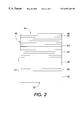
- FIG. 2 shows the cross-section of the semiconductor substrate in FIG. 1 prior to any processing
- FIG. 3 shows a cross-sectional view of the light emitting assembly in FIG. 1 along line 3 — 3 ;
- FIG. 4 shows a top view of a rotating light emitting assembly
- FIG. 5 shows a cross-sectional view of FIG. 4 along line 5 / 5 ;
- FIG. 6 shows a top view of another embodiment of a rotating light emitting assembly
- FIG. 7 shows a top view of a dual color rotating light emitting assembly array
- FIG. 8 shows a cross-sectional view of FIG. 7 along line 8 / 8 .
- FIG. 1 is a top view of a movable stage with a light emitter, actuation mechanism and suspension system integrated with a substrate.
- the light emitter preferably takes the form of any III-V based emitters, for example, vertical cavity surface emitting lasers (VCSELS), light emitting diodes (LEDS), and edge emitting light emitters.
- VCSEL shuttle 1 has movable VCSEL stage 10 which supports VCSEL 12 .
- Stage 10 has one mechanical degree of freedom (x) and is suspended with support members 16 - 19 .
- the III-V material remains on the shuttle structure as shown in the shaded regions 10 and 20 as well as on VCSEL stage 10 .
- VCSEL material is etched away except in the shaded region to expose the n-Si buffer layer to allow the fabrication of comb-drive structures on the n-Si buffer layer
- Support members 16 - 19 may take the form of straight bending springs (as shown), and may also include other configurations known from the silicon art, for example, folded beams.
- Mechanical designs such as ‘folded spring’ suspensions, tapered or stepped comb fingers, x/y folded spring suspensions, archimedian spiral springs for a rotational degree of freedom, etc., which are well-known in silicon structures, may be implemented in the III-V structures.
- the in-plane shape of structures stage, springs, combs
- stage, springs, combs is relatively arbitrary within fairly wide limits.
- stage 10 is moved by applying voltage V 1 between fixed fingers 22 and movable fingers 24 of comb drive 20 at comb drive contact pad 36 and applying a voltage V 2 between fixed fingers 23 and movable fingers 25 of comb drive 21 at comb drive contact pad 37 .
- the fixed fingers are electrically isolated from the movable fingers by isolation grooves 70 and 71 etched down to the oxidation layer 58 .
- the VCSEL and the movable combs share one common ground 44 deposited top of buffer layer 60 .
- Movable fingers 24 and 25 are attached to stage 10 with its integrated VCSEL. 12 and stage 10 is suspended with flexiblesupport members 16 - 19 . Support members 16 - 19 are anchored to substrate 50 at anchor points 30 - 33 , while fixed combs 22 and 23 are anchored to substrate 50 at anchor points 34 and 35 .
- the stage position is proportional to the force, which is proportional to the square of the applied voltage.
- Conductive heat transfer through the suspensionsupport members sinks the waste heat from the VCSEL into the substrate.
- the low threshold current, characteristic for VCSELs makes it possible to keep the temperature of the stage under control.
- conductive line 40 is run from VCSEL contact pad 42 on substrate 50 to stage 10 and to VCSEL 12 .
- Conductive line 40 runs over the neutral fiber of suspensionsupport member 16 , and is electrically isolated from suspensionsupport member 16 .
- the ‘neutral fiber’ is the-stress free centerline of the flexingsupport member.
- the width of conductive line 40 is chosen sufficiently small relative to the width of the support member and runs along the centerline of the support member in order to minimize mechanical stress, which allows conductive line 40 to survive the mechanical scanning motion of the beam.
- the electrical isolation of conductive line 40 from suspensionsupport member 16 may be accomplished in many ways, for example, with a dielectric layer underneath conductive line 40 or insulating the suspension beam surface using shallow ion implantation.
- FIG. 2 is a cross-sectional view of substrate 50 prior to any etching with substrate back side 52 and wafer front side 54 .
- the substrate structure includes layers of doped n-Si substrate 56 , etch stop layer 58 , buffer layer n-type Si 60 , N-type quarter wave distributed Bragg reflector (DBR) mirror layers 62 , active region 64 , P-type DBR mirror 66 and P+ contact layer 68 .
- DBR distributed Bragg reflector
- layer 56 is n-Si substrate, etch stop layer 58 is SiO2, buffer layer 60 is n-Si, n-DBR layer 62 is n-Al x Ga 1 ⁇ x As/Al y Ga 1 ⁇ y As, active layer 64 is a quantum well layer sandwiched by AlGaAs potential confinement layers, P DBR layer is P—Al x Ga 1 ⁇ x As(x ⁇ 0.05)/Al y Ga 1 ⁇ y As(y ⁇ 0.95) and P+ contact layer is GaAs.
- FIG. 3 is a cross sectional view along line 3 — 3 of FIG. 1, and shows the VCSEL structure described in FIG. 2 after the VCSEL structure has been processed or etched.
- the III-V material VCSEL top layer 68 shown
- Etch isolation grooves 70 and 71 are formed in the fabrication process.
- the current of VCSEL 12 flows through the n-GaAs layer in the long suspended beam 18 to the n-Si layer 60 .
- Substrate 50 is etched from the substrate back 52 to provide substrate opening 80 and layers 56 , 58 , 60 , 62 , 64 , 66 and 68 have been removed to form stage openings 82 and 84 .
- Implantation region 41 extends underneath conductive line 40 and is insulating so that the current can only flow into the active region of the VCSEL from VCSEL contact pad 42 .
- Substrate contact 43 is deposited on the corner of the substrate back side 152 .
- the GaAs-based VCSEL structure is bonded on top of a commercially available Simox (Si on insulator) wafer 55 composed of layers 56 , 58 and 60 .
- Simox wafer 55 composed of layers 56 , 58 and 60 .
- An inverted GaAs based VCSEL structure grown on GaAs may be bonded to Simox wafer 55 , using conventional bonding techniques, for example, wafer fusion bonding.
- the bonding can be done through wafer to wafer direct bonding or through an intermediate layer of metal or dielectric. In the case of metal bonding, indium or Ge—Au may be needed. For dielectric, spin-on glass is an example.
- direct wafer bonding is used.
- an InP or InGaP intermediate layer may be used which can be grown on the Si wafer or on top of the VCSEL wafer or both. Examples of useful bonding techniques are taught in U.S. Pat. Nos. 5,728,623 and 5,493,986, which are hereby incorporated by reference.
- the Si/SiO 2 /Si structure will be useful for electrical isolation, which will be discussed in more detail later on.
- the n-Si layer 60 is 10 to 20 ⁇ m thick, which could be thicker to stand the stress in released beams and membranes after wafer bonding
- SiO 2 layer 58 is 500 nm thick
- n-Si layer 56 is 400 ⁇ m thick.
- the GaAs substrate is removed selectively by wet etching, leaving the VCSEL epi-structure of approximately 7 ⁇ m thick on top of the Simox wafer, shaded regions, and stage support members 16 - 19 .
- a scanning light emitting shuttle can be fabricated from substrate 50 using Si-MEMS fabrication technology.
- VCSEL stage 10 is suspended in the center by support members 16 - 19 fabricated from the layer 60 .
- Linear scanning motion of the stage 10 is realized through comb drives 20 and 21 attached to the stage and the Simox substrate 55 , which are fabricated monolithically with the VCSEL table from the Si substrate.
- Comb drive fingers 22 - 25 are fabricated from n-Si layer 60 as well. With a driving voltage across the comb drives, the VCSEL shuttle is scanned in a linear motion with a displacement of tens of micro-meters.
- the VCSEL may be fabricated by oxidation techniques to oxidize an inserted Al x Ga 1 ⁇ x As (x ⁇ 0.98) layer to form an oxide aperture for optical and electrical confinement.
- FIGS. 1 and 3 only one VCSEL is drawn with its p-connect wire running over the center line of one suspended beam. It is possible to put two VCSELs on the shuttle side by side by utilizing another suspension beam.
- Comb fixed fingers 22 and comb movable fingers 24 of comb drive 20 and comb fixed fingers 23 and comb movable fingers 25 of comb drive 21 are electrically isolated from one another. Since the fingers of each comb are of opposite polarities coupled by capacitance only, electrical isolation is needed which has to stand over 100 V electrical bias without breakdown. In one example, this is realized by using etch isolation grooves 70 and 71 to etch down to etch stop layer 58 of about 500 to 1000 nm thick underneath the VCSEL structure,
- V bias voltage
- V 2 bias voltage
- the electric transport property at the bonding interface is very important for low resistance.
- Lo, et al. has reported a series resistance of 100 ohms for a GaAs edge emitting laser flip bonded to a p-Si substrate. Highly doped n-GaAs and n-Si might provide much lower impedance for carrier transport at the interface. If the driving current for the VCSEL is on the order of hundreds of ⁇ A, the voltage drop across the interface would be less than 0.1 volts.
- the VCSEL structure then undergoes ion implantation process for isolation and metallization. Holes flows through the p-DBR region confined by the ion implanted area and into that portion of the active layer which lies below the p-DBR cavity and recombine with electrons flowing upwards from the N-DBR below and producing photon emission and optical amplification. At sufficiently high current flow, this optical amplification in combination with feedback from the DBR mirrors will result in laser oscillation and emission within the VCSEL cavity. Regions formed by the ion implantation isolation process are highly resistive.
- the VCSEL scanners can be packaged in TO-type packages (e.g. 1 VCSEL per package, or more if desirable) with built-in short focal length lens.
- a ‘small’ stage scan length e.g. 5 ⁇ m
- a ‘small’ stage scan length can, within limits, be considerably magnified by placing the VCSEL scanner close to a short focal length lens and using a comparatively large throw distance (e.g. 1′′ optical scan length feasible for a 50 ⁇ m mechanical scan amplitude using a 10 inch or 20 inch throw distance (250 ⁇ , 125 ⁇ respectively).
- FIG. 4 shows a rotating VCSEL fabricated from the bonded structure.
- the VCSEL is bonded to a torsional Si-based actuator, which can be rotated by bias voltages across the bottom electrodes and the Si platform, with an angular rotation range of ⁇ 40°.
- a micro-lens may be placed on top of the VCSEL aperture for beam collimation.
- the lens can be fabricated by any conventional lens fabrication process, such as photoresist reflow or pattern transferring to a SiO 2 layer.
- the Si platform can be rotated two dimensionally as well with another degree of rotation by electrostatic or magnetic actuation.
- VCSEL 112 is supported on stage 110 .
- Semiconductor substrate 150 has VCSEL 112 on stage 110 suspended from suspensionsupport members 114 and 115 . The actuation is done with parallel plate capacitors formed between stage 110 and electrodes 116 and 117 on glass cover 120 .
- “Raster Output Scanner with Pivotal Mirror for Process Direction Light Spot Position Control” U.S. patent application Ser. No. 08/761,681, filed on Dec. 6, 1996 cited earlier, discloses the manufacture and operation of a pivoting mirror, the operation of moving stage 110 being similar in operation to that of the pivoting mirror. Differential actuation of electrodes 116 and 117 produces a ⁇ motion; common actuation of electrodes 116 and 117 produces a z-motion.
- FIG. 5 is a cross-sectional view of FIG. 4, along line 5 — 5 .
- Glass cover 120 is supported above substrate 150 by seal 122 .
- FIG. 6 Another configuration for a rotating light emitting device is a VCSEL 212 on VCSEL stage 210 fabricated on a Si cantilever platform shown in FIG. 6.
- a micro-lens 220 may be placed on top of the VCSEL aperture for beam collimation.
- Microlens 220 can be fabricated by any conventional lens fabrication process, such as photoresist reflow or pattern transferring to a SiO 2 layer.
- the Si platform can be rotated two dimensionally by electrostatic or magnetic actuation.
- VCSEL stage 210 with VCSEL 212 is attached to substrate 250 by cantilever beam 214 .
- the actuation is accomplished by actuating electrode 216 on substrate 250 by applying voltage V.
- Actuation of electrode 216 produces an angular motion of stage 210 in the direction of electrode 216 .
- Conductive line 240 electrically connects VCSEL 212 with contact pad 242 .
- FIG. 7 shows a dual-color rotating VCSEL array. Two or more VCSEL structures of different colors are shown bonded on top of semiconductor substrate 350 .
- the first VCSEL 212 and supporting structure has a configuration similar to that of FIG. 6, with N-type quarter wave distributed Bragg reflector (DBR) mirror layers 262 , active region 264 , P-type DBR mirror 266 .
- DBR distributed Bragg reflector
- VCSEL stage 310 with VCSEL 312 and microlens 320 is attached to substrate 350 by cantilever beam 314 .
- the movement of stage 310 is accomplished by actuating electrode 316 on substrate 350 by applying voltage V 2 .
- Actuation of electrode 316 produces an angular motion of stage 310 in the direction of electrode 316 .
- Conductive line 340 electrically connects VCSEL 312 with contact pad 342 .
- FIG. 8 shows a cross-sectional view of FIG. 7 along line 8 — 8 .
- VCSEL 312 is a different color than VCSEL 212 .
- VCSEL 312 may be fabricated by first bonding one VCSEL wafer, for example a red VCSEL, with N-type quarter wave distributed Bragg reflector (DBR) mirror layers 362 , P-type DBR mirror 366 to the Simox substrate 355 and then removing the substrate of the red VCSEL, followed by bonding of another VCSEL, for example an infrared VCSEL, with N-type quarter wave distributed Bragg reflector (DBR) mirror layers 370 , active region 372 , P-type DBR mirror 374 on top of the first VCSEL wafer.
- DBR distributed Bragg reflector
Abstract
Description
Claims (15)
Priority Applications (1)
| Application Number | Priority Date | Filing Date | Title |
|---|---|---|---|
| US09/210,315 US6567448B1 (en) | 1997-12-12 | 1998-12-11 | Scanning III-V compound light emitters integrated with Si-based actuators |
Applications Claiming Priority (2)
| Application Number | Priority Date | Filing Date | Title |
|---|---|---|---|
| US6956997P | 1997-12-12 | 1997-12-12 | |
| US09/210,315 US6567448B1 (en) | 1997-12-12 | 1998-12-11 | Scanning III-V compound light emitters integrated with Si-based actuators |
Publications (1)
| Publication Number | Publication Date |
|---|---|
| US6567448B1 true US6567448B1 (en) | 2003-05-20 |
Family
ID=26750212
Family Applications (1)
| Application Number | Title | Priority Date | Filing Date |
|---|---|---|---|
| US09/210,315 Expired - Lifetime US6567448B1 (en) | 1997-12-12 | 1998-12-11 | Scanning III-V compound light emitters integrated with Si-based actuators |
Country Status (1)
| Country | Link |
|---|---|
| US (1) | US6567448B1 (en) |
Cited By (8)
| Publication number | Priority date | Publication date | Assignee | Title |
|---|---|---|---|---|
| US20030118068A1 (en) * | 2001-12-20 | 2003-06-26 | Johnson Ralph H. | Vertical cavity surface emitting laser including indium and nitrogen in the active region |
| US6727562B2 (en) * | 2002-01-22 | 2004-04-27 | Intpax, Inc. | Basic common optical cell configuration of dual cavities for optical tunable devices |
| US20050052723A1 (en) * | 2003-07-22 | 2005-03-10 | Shin-Ichiro Watanabe | Electrostatic comb drive actuator, and optical controller using the electrostatic comb drive actuator |
| US20050094963A1 (en) * | 2003-11-03 | 2005-05-05 | Jidong Hou | Tunable optical device |
| US20070201525A1 (en) * | 2004-10-01 | 2007-08-30 | Finisar Corporation | Vertical cavity surface emitting laser having strain reduced quantum wells |
| US7339454B1 (en) * | 2005-04-11 | 2008-03-04 | Sandia Corporation | Tensile-stressed microelectromechanical apparatus and microelectromechanical relay formed therefrom |
| US20110090930A1 (en) * | 2004-10-01 | 2011-04-21 | Finisar Corporation | Vertical cavity surface emitting laser with undoped top mirror |
| US20170085056A1 (en) * | 2015-09-18 | 2017-03-23 | Skorpios Technologies, Inc. | Semiconductor layer variation for substrate removal after bonding |
Citations (9)
| Publication number | Priority date | Publication date | Assignee | Title |
|---|---|---|---|---|
| US4447136A (en) * | 1980-07-18 | 1984-05-08 | Canon Kabushiki Kaisha | Semi-conductor laser device |
| US5025346A (en) | 1989-02-17 | 1991-06-18 | Regents Of The University Of California | Laterally driven resonant microstructures |
| US5055731A (en) * | 1989-08-02 | 1991-10-08 | Hitachi, Ltd. | High-speed two-dimensional electrostatic actuator |
| US5536988A (en) | 1993-06-01 | 1996-07-16 | Cornell Research Foundation, Inc. | Compound stage MEM actuator suspended for multidimensional motion |
| US5628917A (en) | 1995-02-03 | 1997-05-13 | Cornell Research Foundation, Inc. | Masking process for fabricating ultra-high aspect ratio, wafer-free micro-opto-electromechanical structures |
| US5640133A (en) | 1995-06-23 | 1997-06-17 | Cornell Research Foundation, Inc. | Capacitance based tunable micromechanical resonators |
| US5719891A (en) | 1995-12-18 | 1998-02-17 | Picolight Incorporated | Conductive element with lateral oxidation barrier |
| US5747366A (en) | 1995-12-27 | 1998-05-05 | Alcatel Alsthom Compagnie Generale D'electricite | Method of fabricating a surface emitting semiconductor laser |
| US5764671A (en) | 1996-10-21 | 1998-06-09 | Motorola, Inc. | VCSEL with selective oxide transition regions |
-
1998
- 1998-12-11 US US09/210,315 patent/US6567448B1/en not_active Expired - Lifetime
Patent Citations (9)
| Publication number | Priority date | Publication date | Assignee | Title |
|---|---|---|---|---|
| US4447136A (en) * | 1980-07-18 | 1984-05-08 | Canon Kabushiki Kaisha | Semi-conductor laser device |
| US5025346A (en) | 1989-02-17 | 1991-06-18 | Regents Of The University Of California | Laterally driven resonant microstructures |
| US5055731A (en) * | 1989-08-02 | 1991-10-08 | Hitachi, Ltd. | High-speed two-dimensional electrostatic actuator |
| US5536988A (en) | 1993-06-01 | 1996-07-16 | Cornell Research Foundation, Inc. | Compound stage MEM actuator suspended for multidimensional motion |
| US5628917A (en) | 1995-02-03 | 1997-05-13 | Cornell Research Foundation, Inc. | Masking process for fabricating ultra-high aspect ratio, wafer-free micro-opto-electromechanical structures |
| US5640133A (en) | 1995-06-23 | 1997-06-17 | Cornell Research Foundation, Inc. | Capacitance based tunable micromechanical resonators |
| US5719891A (en) | 1995-12-18 | 1998-02-17 | Picolight Incorporated | Conductive element with lateral oxidation barrier |
| US5747366A (en) | 1995-12-27 | 1998-05-05 | Alcatel Alsthom Compagnie Generale D'electricite | Method of fabricating a surface emitting semiconductor laser |
| US5764671A (en) | 1996-10-21 | 1998-06-09 | Motorola, Inc. | VCSEL with selective oxide transition regions |
Non-Patent Citations (8)
| Title |
|---|
| "Electrostatic-comb Drive of Lateral Polysilicon Resonators", by William C. Tang, Tu-Cuong H. Nguyen, Michael W. Judy & Roger W. Howe, Transducers '89, Proceedings of the 5th International Conference on Solid-State Sensors and Actuators and Eurosensors III, vol. 2, pp. 328-331, Jun., 1990. |
| "Fabrication of Submicron High-Aspect-Ratio GaAs Actuators", by Z. Lisa Zhang & Noel C. MacDonald, Journal of Microelectromechanical Systems, vol. 2, No. 3, Jun., 1993, pp. 66-73. |
| "Integration of GaAs Vertical-Cavity Surface Emitting Laser on Si by Substrate Removal", by Hsi-Jen J. Yeh and John S. Smith, Appl. Phys. Lett., vol. 64, No. 12, Mar. 12, 1994, pp. 1466-1468. |
| "Laterally Driven Polysilicon Resonant Microstructures", by William C. Tang, Tu-Cuong H. Nguyen and Roger T. Howe, Proceedings IEEE Micro Electro Mechanical Systems, pp. 53-59, Feb., 1989. |
| "Semiconductor Lasers on Si Substrates Using the Technology of Bonding by Atomic Rearrangement" by Y.H. Lo, R. Bhat and D.M. Hwang, C. Chua and C.H. Lin, Appl. Phys. Lett., vol. 62. No. 10, Mar. 8, 1993, pp. 1038-1040. |
| U.S. patent application Ser. No. 08/761,681, entitled "Raster Output Scanner with Pivotal Mirror for Process Direction Light Spot Position Control" filed on Dec. 6, 1996. |
| U.S. patent application Ser. No. 08/940,867, entitled "Highly Compact Vertical Cavity Surface Emitting Lasers" filed Sep. 30, 1997. |
| U.S. patent application Ser. No. 09/173,329, entitled "Monolithic Scanning Light Emitting Devices", filed on Oct. 15, 1998. |
Cited By (13)
| Publication number | Priority date | Publication date | Assignee | Title |
|---|---|---|---|---|
| US7408964B2 (en) * | 2001-12-20 | 2008-08-05 | Finisar Corporation | Vertical cavity surface emitting laser including indium and nitrogen in the active region |
| US20030118068A1 (en) * | 2001-12-20 | 2003-06-26 | Johnson Ralph H. | Vertical cavity surface emitting laser including indium and nitrogen in the active region |
| US6727562B2 (en) * | 2002-01-22 | 2004-04-27 | Intpax, Inc. | Basic common optical cell configuration of dual cavities for optical tunable devices |
| US20050052723A1 (en) * | 2003-07-22 | 2005-03-10 | Shin-Ichiro Watanabe | Electrostatic comb drive actuator, and optical controller using the electrostatic comb drive actuator |
| US20050094963A1 (en) * | 2003-11-03 | 2005-05-05 | Jidong Hou | Tunable optical device |
| US7269325B2 (en) * | 2003-11-03 | 2007-09-11 | Jidong Hou | Tunable optical device |
| US8168456B2 (en) | 2004-10-01 | 2012-05-01 | Finisar Corporation | Vertical cavity surface emitting laser with undoped top mirror |
| US20110090930A1 (en) * | 2004-10-01 | 2011-04-21 | Finisar Corporation | Vertical cavity surface emitting laser with undoped top mirror |
| US20070201525A1 (en) * | 2004-10-01 | 2007-08-30 | Finisar Corporation | Vertical cavity surface emitting laser having strain reduced quantum wells |
| US8451875B2 (en) | 2004-10-01 | 2013-05-28 | Finisar Corporation | Vertical cavity surface emitting laser having strain reduced quantum wells |
| US7339454B1 (en) * | 2005-04-11 | 2008-03-04 | Sandia Corporation | Tensile-stressed microelectromechanical apparatus and microelectromechanical relay formed therefrom |
| US20170085056A1 (en) * | 2015-09-18 | 2017-03-23 | Skorpios Technologies, Inc. | Semiconductor layer variation for substrate removal after bonding |
| US10243314B2 (en) * | 2015-09-18 | 2019-03-26 | Skorpios Technologies, Inc. | Semiconductor layer variation for substrate removal after bonding |
Similar Documents
| Publication | Publication Date | Title |
|---|---|---|
| US6054335A (en) | Fabrication of scanning III-V compound light emitters integrated with Si-based actuators | |
| US6116756A (en) | Monolithic scanning light emitting devices | |
| US6180428B1 (en) | Monolithic scanning light emitting devices using micromachining | |
| JP3805522B2 (en) | Long wavelength emitting vertical cavity surface emitting laser and method of manufacturing the same | |
| EP0896405B1 (en) | Method for fabricating surface-emitting semiconductor device | |
| US6091537A (en) | Electro-actuated microlens assemblies | |
| US6658041B2 (en) | Wafer bonded vertical cavity surface emitting laser systems | |
| US5031187A (en) | Planar array of vertical-cavity, surface-emitting lasers | |
| US5877038A (en) | Method of making a vertical cavity laser | |
| US6570905B1 (en) | Vertical cavity surface emitting laser with reduced parasitic capacitance | |
| US11482835B2 (en) | VCSEL device with multiple stacked active regions | |
| US20030169786A1 (en) | Micro-electromechanically tunable vertical cavity photonic device and a method of fabrication thereof | |
| US20230008483A1 (en) | Vertical cavity surface emitting laser element, vertical cavity surface emitting laser element array, vertical cavity surface emitting laser module, and method of producing vertical cavity surface emitting laser element | |
| KR20030084994A (en) | A micro-electromechanically tunable vertical cavity photonic device and a method of fabrication thereof | |
| US6567448B1 (en) | Scanning III-V compound light emitters integrated with Si-based actuators | |
| US11322910B2 (en) | Indium-phosphide VCSEL with dielectric DBR | |
| JPH0793419B2 (en) | Light receiving and emitting integrated device | |
| JP2000196189A (en) | Surface-emission semiconductor laser | |
| KR20020026990A (en) | Vertical cavity surface emitting laser having micro-lens | |
| JP4437376B2 (en) | Manufacturing method of surface emitting laser element | |
| JPH02208067A (en) | Optical scanner | |
| Choquette et al. | Short wavelength bottom-emitting vertical cavity lasers fabricated using wafer bonding | |
| JP4040324B2 (en) | Mirror, optical switch using the same, and manufacturing method thereof | |
| JP4387485B2 (en) | Light source device for emitting evanescent light | |
| JP2004087903A (en) | Surface-emitting laser |
Legal Events
| Date | Code | Title | Description |
|---|---|---|---|
| AS | Assignment |
Owner name: XEROX CORPORATION, CONNECTICUT Free format text: ASSIGNMENT OF ASSIGNORS INTEREST;ASSIGNORS:SUN, DECAI;BRINGANS, ROSS D.;CHUA, CHRISTOPHER L.;AND OTHERS;REEL/FRAME:009644/0821;SIGNING DATES FROM 19981208 TO 19981209 |
|
| AS | Assignment |
Owner name: BANK ONE, NA, AS ADMINISTRATIVE AGENT, ILLINOIS Free format text: SECURITY AGREEMENT;ASSIGNOR:XEROX CORPORATION;REEL/FRAME:013111/0001 Effective date: 20020621 Owner name: BANK ONE, NA, AS ADMINISTRATIVE AGENT,ILLINOIS Free format text: SECURITY AGREEMENT;ASSIGNOR:XEROX CORPORATION;REEL/FRAME:013111/0001 Effective date: 20020621 |
|
| STCF | Information on status: patent grant |
Free format text: PATENTED CASE |
|
| AS | Assignment |
Owner name: JPMORGAN CHASE BANK, AS COLLATERAL AGENT, TEXAS Free format text: SECURITY AGREEMENT;ASSIGNOR:XEROX CORPORATION;REEL/FRAME:015134/0476 Effective date: 20030625 Owner name: JPMORGAN CHASE BANK, AS COLLATERAL AGENT,TEXAS Free format text: SECURITY AGREEMENT;ASSIGNOR:XEROX CORPORATION;REEL/FRAME:015134/0476 Effective date: 20030625 |
|
| FPAY | Fee payment |
Year of fee payment: 4 |
|
| CC | Certificate of correction | ||
| FPAY | Fee payment |
Year of fee payment: 8 |
|
| FPAY | Fee payment |
Year of fee payment: 12 |
|
| AS | Assignment |
Owner name: XEROX CORPORATION, NEW YORK Free format text: RELEASE BY SECURED PARTY;ASSIGNOR:BANK ONE, NA;REEL/FRAME:034782/0644 Effective date: 20030625 Owner name: XEROX CORPORATION, NEW YORK Free format text: RELEASE BY SECURED PARTY;ASSIGNOR:JPMORGAN CHASE BANK, N.A.;REEL/FRAME:034782/0816 Effective date: 20061204 |
|
| AS | Assignment |
Owner name: XEROX CORPORATION, CONNECTICUT Free format text: RELEASE BY SECURED PARTY;ASSIGNOR:JPMORGAN CHASE BANK, N.A. AS SUCCESSOR-IN-INTEREST ADMINISTRATIVE AGENT AND COLLATERAL AGENT TO BANK ONE, N.A.;REEL/FRAME:061388/0388 Effective date: 20220822 Owner name: XEROX CORPORATION, CONNECTICUT Free format text: RELEASE BY SECURED PARTY;ASSIGNOR:JPMORGAN CHASE BANK, N.A. AS SUCCESSOR-IN-INTEREST ADMINISTRATIVE AGENT AND COLLATERAL AGENT TO JPMORGAN CHASE BANK;REEL/FRAME:066728/0193 Effective date: 20220822 |