US6587511B2 - Radio frequency transmitter and methods thereof - Google Patents
Radio frequency transmitter and methods thereof Download PDFInfo
- Publication number
- US6587511B2 US6587511B2 US09/769,444 US76944401A US6587511B2 US 6587511 B2 US6587511 B2 US 6587511B2 US 76944401 A US76944401 A US 76944401A US 6587511 B2 US6587511 B2 US 6587511B2
- Authority
- US
- United States
- Prior art keywords
- power level
- signals
- output signal
- targeted
- relative phase
- Prior art date
- Legal status (The legal status is an assumption and is not a legal conclusion. Google has not performed a legal analysis and makes no representation as to the accuracy of the status listed.)
- Expired - Lifetime, expires
Links
Images


Classifications
-
- H—ELECTRICITY
- H03—ELECTRONIC CIRCUITRY
- H03F—AMPLIFIERS
- H03F1/00—Details of amplifiers with only discharge tubes, only semiconductor devices or only unspecified devices as amplifying elements
- H03F1/02—Modifications of amplifiers to raise the efficiency, e.g. gliding Class A stages, use of an auxiliary oscillation
- H03F1/0205—Modifications of amplifiers to raise the efficiency, e.g. gliding Class A stages, use of an auxiliary oscillation in transistor amplifiers
- H03F1/0294—Modifications of amplifiers to raise the efficiency, e.g. gliding Class A stages, use of an auxiliary oscillation in transistor amplifiers using vector summing of two or more constant amplitude phase-modulated signals
-
- H—ELECTRICITY
- H03—ELECTRONIC CIRCUITRY
- H03F—AMPLIFIERS
- H03F1/00—Details of amplifiers with only discharge tubes, only semiconductor devices or only unspecified devices as amplifying elements
- H03F1/02—Modifications of amplifiers to raise the efficiency, e.g. gliding Class A stages, use of an auxiliary oscillation
-
- H—ELECTRICITY
- H03—ELECTRONIC CIRCUITRY
- H03F—AMPLIFIERS
- H03F3/00—Amplifiers with only discharge tubes or only semiconductor devices as amplifying elements
- H03F3/20—Power amplifiers, e.g. Class B amplifiers, Class C amplifiers
- H03F3/24—Power amplifiers, e.g. Class B amplifiers, Class C amplifiers of transmitter output stages
-
- H—ELECTRICITY
- H03—ELECTRONIC CIRCUITRY
- H03G—CONTROL OF AMPLIFICATION
- H03G3/00—Gain control in amplifiers or frequency changers without distortion of the input signal
- H03G3/20—Automatic control
- H03G3/30—Automatic control in amplifiers having semiconductor devices
- H03G3/3036—Automatic control in amplifiers having semiconductor devices in high-frequency amplifiers or in frequency-changers
- H03G3/3042—Automatic control in amplifiers having semiconductor devices in high-frequency amplifiers or in frequency-changers in modulators, frequency-changers, transmitters or power amplifiers
-
- H—ELECTRICITY
- H04—ELECTRIC COMMUNICATION TECHNIQUE
- H04B—TRANSMISSION
- H04B1/00—Details of transmission systems, not covered by a single one of groups H04B3/00 - H04B13/00; Details of transmission systems not characterised by the medium used for transmission
- H04B1/02—Transmitters
- H04B1/04—Circuits
- H04B2001/0408—Circuits with power amplifiers
- H04B2001/045—Circuits with power amplifiers with means for improving efficiency
-
- H—ELECTRICITY
- H04—ELECTRIC COMMUNICATION TECHNIQUE
- H04W—WIRELESS COMMUNICATION NETWORKS
- H04W52/00—Power management, e.g. TPC [Transmission Power Control], power saving or power classes
- H04W52/04—TPC
Definitions
- Modern systems enable radio transmitters to transmit at reduced power for long periods of time.
- the modulating signal of these transmissions may have large peak-to-minimum amplitude variations. Since the efficiency of power amplifiers is generally reduced at less-than-maximum power levels, these two factors may increase the average current consumption of power amplifiers in radio transmitters.
- FIG. 1 is a schematic block-diagram illustration of an exemplary radio frequency transmitter, according to an embodiment of the present invention
- FIGS. 2A and 2B are schematic illustrations of signal space diagrams, helpful in understanding the present invention.
- FIG. 3 is a schematic block-diagram illustration of an exemplary up-conversion chain, according to an embodiment of the present invention.
- FIGS. 4A, 4 B and 4 C are exemplary graphical illustrations of the instantaneous efficiency of the radio frequency transmitter of FIG. 1 and of a conventional class-B power amplifier as a function of the instantaneous output signal power due to the amplitude of the modulating signal;
- FIG. 5 is a schematic block-diagram illustration of an exemplary radio frequency transmitter, according to another embodiment of the present invention.
- FIG. 6A is an exemplary graphical illustration of the instantaneous efficiency of the radio frequency transmitter of FIG. 1 for a constant envelope signal as a function of the output signal power, according to another embodiment of the present invention.
- FIG. 6B is an exemplary graphical illustration of the instantaneous efficiency of the radio frequency transmitter of FIG. 1 for a non-constant envelope signal as a function of the output signal power, according to a further embodiment of the present invention.
- the present invention may be used in a variety of applications. Although the present invention is not limited in this respect, the circuit disclosed herein may be used in many apparatuses such as in the transmitters of a radio system. Radio systems intended to be included within the scope of the present invention include, by way of example only, cellular radiotelephone communication systems, two-way radio communication systems, one-way pagers, two-way pagers, personal communication systems (PCS), and the like.
- Radio systems intended to be included within the scope of the present invention include, by way of example only, cellular radiotelephone communication systems, two-way radio communication systems, one-way pagers, two-way pagers, personal communication systems (PCS), and the like.
- Types of cellular radiotelephone communication systems intended to be within the scope of the present invention include, although are not limited to, Direct Sequence-Code Division Multiple Access (DS-CDMA) cellular radiotelephone communication systems, Wideband CDMA (WBCDMA) and CDMA2000 cellular radiotelephone systems, Global System for Mobile Communications (GSM) cellular radiotelephone systems, North American Digital Cellular (NADC) cellular radiotelephone systems, Time Division Multiple Access (TDMA) systems, Enhanced Data for GSM Evolution (EDGE) and Universal Mobile Telecommunications Systems (UMTS).
- DS-CDMA Direct Sequence-Code Division Multiple Access
- WBCDMA Wideband CDMA
- CDMA2000 Code Division Multiple Access
- GSM Global System for Mobile Communications
- NADC North American Digital Cellular
- TDMA Time Division Multiple Access
- EDGE Enhanced Data for GSM Evolution
- UMTS Universal Mobile Telecommunications Systems
- An RF transmitter 100 may comprise a digital signal processor (DSP) 102 , baseband (BB) to RF up-conversion chains 104 and 106 , RF preamplifiers 108 and 110 , a power amplifier 112 , an antenna 114 and a controller 116 .
- DSP digital signal processor
- BB baseband
- a BB input signal 118 may be provided to DSP 102 , which may convert it into two constant envelope vectors according to a method which will be described hereinbelow with respect to FIGS. 2A and 2B.
- the first constant envelope vector may be represented by baseband signals I 1 and Q 1
- the second constant envelope vector may be represented by baseband signals I 2 and Q 2 .
- Up-conversion chain 104 may convert signals I 1 and Q 1 into an RF signal RF 1 ; similarly up-conversion chain 106 may convert signals I 2 and Q 2 into an RF signal RF 2 .
- RF signals RF 1 and RF 2 have a common carrier frequency.
- An exemplary embodiment of up-conversion chains 104 and 106 is described hereinbelow with respect to FIG. 3, although the present invention is in no way limited to this particular exemplary embodiment.
- RF preamplifier 108 which has a variable gain, may amplify signal RF 1 to produce a signal RF IN-1 ; similarly RF preamplifier 110 , which has a variable gain, may amplify signal RF 2 to produce a signal RF IN-2 .
- Power amplifier 112 which may have reactive termination, may amplify and combine RF IN-1 and RF IN-2 to produce an output signal RF OUT for transmission by antenna 114 .
- Power amplifier 112 may comprise two branch amplifiers 120 and 122 connected in parallel, and shunt reactance elements 124 and 126 at the output of branch amplifiers 120 and 122 , respectively.
- B S denotes the shunt reactance of element 124
- -B S denotes the shunt reactance of element 126 .
- the efficiency of power amplifier 112 at a specific output signal power may be improved by adjusting the shunt reactance B S .
- Power amplifier 112 may also comprise a transmission-line-coupler 128 for combining the outputs of branch amplifiers 120 and 122 .
- Transmission-line-coupler 128 may comprise two transmission lines 130 and 132 connected to antenna 114 so that the sum of the branch currents goes through the load.
- Other combiner schemes yielding the same performance may be implemented instead, namely hybrid BALUN, center tap inductor, etc.
- Controller 116 may receive as input a targeted average output signal power level P.
- Targeted average output signal power level P may be selected from a range of power levels or may be selected from a discrete set of at least two power levels.
- Controller 116 may provide data related to P to any of DSP 102 , up-conversion chains 104 and 106 , and RF preamplifiers 108 and 110 , with the result that power amplifier 112 may produce an output signal whose average power is substantially equivalent to P.
- FIGS. 2A and 2B are schematic illustrations of signal space diagrams.
- the horizontal axis of the diagram represents the real (in-phase) component of a signal vector, while the vertical axis of the diagram represents the imaginary (quadrature) component.
- FIG. 2A Three concentric circles, 202 , 204 and 206 , are shown in FIG. 2A.
- a vector 208 from the center of the diagram to the largest circle 206 represents the amplitude and phase of a BB signal, which after up-conversion and amplification may produce a signal having a maximal instantaneous output signal power.
- This maximal instantaneous output signal power may be determined both by the maximum amplitude A MAX of input signal 118 (FIG. 1) and by the maximum average power P MAX that power amplifier 112 may be able to produce.
- a vector 210 from the center of the diagram to circle 202 represents the amplitude and phase of a BB signal, which after up-conversion and amplification may produce a signal at an instantaneous output signal power that may be determined both by the minimum amplitude A MIN of input signal 118 and by an average output signal power level P TH , the determination of which will be explained hereinbelow.
- controller 116 may provide DSP 102 with ⁇ (P) so that DSP 102 may represent a baseband vector 212 by two constant envelope vectors 214 and 216 . Since baseband vector 212 has an average amplitude controlled by ⁇ (P), baseband vector 212 may result, after up-conversion and amplification, in a signal at an average output signal power P and at an instantaneous output signal power determined both by the instantaneous amplitude A(t) of input signal 118 and by the targeted average output signal power level P.
- the radius of circle 204 is predetermined both by the maximum amplitude A MAX and by ⁇ (P MAX ).
- the data flow from controller 116 to DSP 102 is indicated in FIG. 1 by line 133 , and constant envelope vectors 214 and 216 are represented by the signals I 1 and Q 1 , and I 2 and Q 2 , respectively.
- BB input signal 118 at time t is denoted s(t), with the real (in-phase) component denoted I(t) and the imaginary (quadrature) component denoted Q(t), then the following decomposition holds:
- a ( t ) ⁇ square root over ( I 2 ( t )+ Q 2 ( t )) ⁇ .
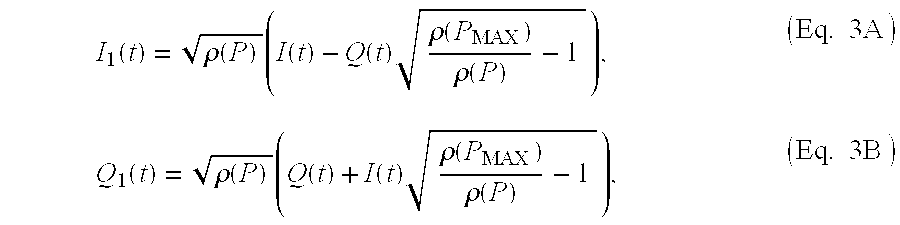
- I 2 ⁇ ( t ) ⁇ ⁇ ( P ) ⁇ ( I ⁇ ( t ) + Q ⁇ ( t ) ⁇ ⁇ ⁇ ( P MAX ) ⁇ A MAX 2 ⁇ ⁇ ( P ) ⁇ A 2 ⁇ ( t ) - 1 ) , ( Eq.
- Equations 1A, 1B, 2A and 2B that the amplitude of the signal represented by I 1 and Q 1 , namely ⁇ square root over (I 1 2 +Q 1 2 ) ⁇ , and the amplitude of the signal represented by I 2 and Q 2 , namely ⁇ square root over (I 2 2 +Q 2 2 ) ⁇ , are both equal to ⁇ square root over ( ⁇ (P MAX )) ⁇ A MAX . It will also be appreciated by persons of ordinary skill in the art that the relative phase differences of these signals are determined from the instantaneous amplitude of input signal 118 and from the targeted average output signal power level P.
- Equation 1A, 1B, 2A and 2B any other set of equations yielding a constant envelope signal represented by signals I 1 and Q 1 , and a constant envelope signal represented by signals I 2 and Q 2 , is clearly also within the scope of the present invention.
- controller 116 may provide predetermined, fixed values to any amplification elements of up-conversion chains 104 and 106 and to RF preamplifiers 108 and 110 .
- the data flow from controller 116 to up-conversion chains 104 and 106 are indicated in FIG. 1 by lines 134 and 136 , respectively.
- Lines 138 and 140 indicate the data flow from controller 116 to RF preamplifiers 108 and 110 , respectively.
- Circles 202 and 204 are the same or similar to those shown in FIG. 2A.
- a vector 220 from the center of the diagram to circle 218 represents the amplitude and phase of a BB signal, which after up-conversion and amplification may produce a signal at an instantaneous output signal power that may be determined both by the maximum amplitude A MAX of input signal 118 (FIG. 1) and by the average output signal power level P TH .
- controller 116 may provide DSP 102 with the power ⁇ (P TH ) so that DSP 102 may represent a baseband vector 222 by two constant envelope vectors 224 and 226 , where the size of constant envelope 204 is the same or similar to that used in FIG. 2 A.
- Constant envelope vectors 224 and 226 may be represented by signals I 1 and Q 1 , and I 2 and Q 2 , respectively, where Equations 1A, 1B, 2A and 2B are used with ⁇ (P TH ) in place of ⁇ (P).
- controller 116 may reduce the amplitudes of signals I 1 and Q 1 , and I 2 and Q 2 , or may reduce the gain of any of variable amplification elements in up-conversion chains 104 and 106 and RF preamplifiers 108 and 110 , or a combination thereof, with the result that power amplifier 112 may produce an output signal whose average power is substantially equivalent to P.
- the predetermined average output signal power level P TH may act as a threshold between two modes of operation of the RF transmitter, according to some embodiments of the present invention.
- the RF transmitter may control the instantaneous output signal power by combining constant envelope signals whose relative phase differences are determined from the instantaneous amplitude of a baseband input signal and from the targeted average output signal power level P, and by up-converting at a fixed gain.
- the RF transmitter may control the instantaneous output signal power by combining constant envelope signals whose relative phase differences are determined from the instantaneous amplitude of the baseband input signal and from the predetermined average output signal power level P TH , and by up-converting at a variable gain which is dependent on the targeted average output signal power level P and which is lower than the fixed gain of the first mode.
- the RF transmitter may control the instantaneous output signal power by combining constant envelope signals whose relative phase differences are determined from the instantaneous amplitude of the baseband input signal and from the predetermined average output signal power level P TH , and whose amplitudes have been reduced in the baseband according to the targeted average output signal power level P, so that the average power of the output signal is substantially equivalent to the targeted average output signal power level P.
- the up-conversion chain may comprise an intermediate frequency (IF) local oscillator (LO) 300 and an RF local oscillator 302 , IQ modulators 304 and 306 , and phase lock loops (PLL) 308 and 310 .
- IF intermediate frequency
- LO local oscillator
- PLL phase lock loops
- IQ modulator 304 may comprise mixers 312 and 314 and combiner 316 .
- Mixer 312 may receive as input I 1 and sin ( ⁇ IF t), where ⁇ IF denotes the frequency generated by IF LO 300 and t denotes time.
- Mixer 314 may receive as input Q 1 and cos ( ⁇ IF t).
- Combiner 316 may combine the outputs of mixers 312 and 314 , and provides the combination to PLL 308 .
- IQ modulator 306 may comprise mixers 318 and 320 and combiner 322 .
- Mixer 318 may receive as input I 2 and sin ( ⁇ IF t).
- Mixer 320 may receive as input Q 2 and cos ( ⁇ IF t).
- Combiner 322 may combine the outputs of mixers 318 and 320 , and provides the combination to PLL 310 .
- PLL 308 may comprise a phase detector (PD) 324 , a loop filter 326 and a voltage-controlled oscillator (VCO) 328 .
- PLL 308 may also comprise a mixer 330 , mixing the output of VCO 328 with the signal produced by RF LO 302 , and providing an IF modulated signal to PD 324 .
- PLL 310 may comprise a PD 334 , a loop filter 336 and a VCO 338 .
- PLL 310 may also comprise a mixer 340 , mixing the output of VCO 338 with the signal produced by RF LO 302 , and providing an IF modulated signal to PD 334 .
- the up-conversion chain may comprise variable amplifiers (not shown) that amplify the input signals I 1 and Q 1 , and I 2 and Q 2 , prior to their modulation by IQ modulators 304 and 306 , respectively.
- the gain of these variable amplifiers may be reduced by controller 116 (not shown) when the targeted average output signal power level P is less than the predetermined power level P TH .
- FIGS. 4A, 4 B and 4 C are exemplary graphical illustrations of the instantaneous efficiency of the radio frequency transmitter of FIG. 1 (indicated by a solid line) and of a conventional class-B power amplifier (indicated by a dotted line) as a function of the output signal power.
- the average output signal power (indicated by a circle) is P MAX
- the instantaneous output signal power (indicated by the solid and dotted lines) varies according to the amplitude of the input signal.
- the average output signal power is P TH
- FIG. 4C the average output signal power is less than P TH .
- the average current consumption of the RF transmitter of FIG. 1 may be appreciably reduced with respect to that of class-B power amplifiers.
- P TH is chosen to be the average output signal power at which the efficiency has a peak value.
- the threshold P TH may be chosen by minimizing the current consumption according to the output signal power probability distribution and the amplitude distribution of the baseband input signal.
- FIG. 5 is a schematic block-diagram illustration of an exemplary radio frequency transmitter, according to another embodiment of the present invention.
- An RF transmitter 500 may comprise DSP 102 , RF preamplifiers 108 and 110 , power amplifier 112 , antenna 114 and controller 116 . As in FIG. 1, BB input signal 118 may be provided to DSP 102 . RF transmitter 500 may also comprise IF local oscillator 300 , RF local oscillator 302 , IQ modulators 304 and 306 , and PLLs 308 and 310 .
- RF transmitter 500 may also comprise a feedback path to compensate for circuit imperfections that may occur in an open loop arrangement such as that of FIG. 1 .
- DSP 102 may comprise a compensation module 502 .
- a small portion of the transmitted signal RF OUT may be taken through a directional coupler 504 via a step attenuator 506 .
- the state of step attenuator 506 may be controlled by controller 116 , as indicated by line 507 , in order to divide the entire dynamic range into several smaller regions.
- the output of step attenuator 506 passes through an image rejection mixer (IRM) 508 .
- IRM 508 down-converts the RF signal to IF.
- IRM 508 may receive as input, in addition to the RF signal, a signal from RF local oscillator 302 .
- the IF signal produced by IRM 508 may be demodulated by an I/Q demodulator 510 , which may receive as input a signal from IF local oscillator 300 .
- I/Q demodulator 510 may produce feedback signals I FB and Q FB , which may be provided to DSP 102 through analog-to-digital converters (not shown).
- controller 116 may provide DSP 102 with a power level ⁇ .
- a power level ⁇ As explained hereinabove, when the targeted average output signal power level P is in a first range of average output signal power levels, i.e. between P MAX and P TH , then the power level ⁇ is related to the targeted average output signal power level P. When the targeted average output signal power level P is in a second range of average output signal power levels, i.e. less than P TH , then the power level ⁇ is related to the predetermined average output signal power level P TH .
- Compensation module 502 may compare the input signal 118 , the feedback signals I FB and Q FB , the power level ⁇ and the state 507 of step attenuator 506 to create the compensated baseband signals I 1 and Q 1 , and I 2 and Q 2 .
- RF transmitter 500 may also comprise a power level measurement unit 512 that may take a small portion of the output of step attenuator 506 through a directional coupler 514 .
- Power level measurement unit 512 may provide a measured power level P FB to controller 116 .
- Controller 116 may compare the targeted output signal power level with measured power level P FB in order to set the targeted amplification values for RF preamplifiers 108 and 110 and for the amplification elements in the up-conversion chains.
- the amplitude of the signal represented by I 1 and Q 1 namely ⁇ square root over (I 1 2 +Q 1 2 ) ⁇
- the amplitude of the signal represented by I 2 and Q 2 namely ⁇ square root over (I 2 2 +Q 2 2 ) ⁇
- their amplitude depends on the amplitude of the input signal and the maximal average output signal power and does not depend on the average output signal power.
- These signals are constant envelope signals only if the input signal is a constant envelope signal. It will also be appreciated by persons of ordinary skill in the art that the relative phase differences of these signals are determined from the targeted average output signal power level P and not from the instantaneous amplitude of input signal 118 .
- FIG. 6A an exemplary graphical illustration of the efficiency of the radio frequency transmitter of FIG. 1 as a function of the output signal power is shown in FIG. 6A, to which reference is now made.
- the efficiency has a peak at two output signal powers.
- the predetermined average output signal power level P TH may be set to be close to the lower of these output signal powers having a peak efficiency.
- the amplitudes of baseband signals I 1 and Q 1 , and I 2 and Q 2 are determined from the instantaneous amplitude A(t) of baseband input signal 118 , and the relative phase differences of baseband signals I 1 and Q 1 , and I 2 and Q 2 , are determined from the targeted output signal power level P.
- the average efficiency of the radio frequency transmitter of FIG. 1 for this embodiment as a function of the output signal power is shown in FIG. 6 B.
Abstract
Description


Claims (26)
Priority Applications (7)
| Application Number | Priority Date | Filing Date | Title |
|---|---|---|---|
| US09/769,444 US6587511B2 (en) | 2001-01-26 | 2001-01-26 | Radio frequency transmitter and methods thereof |
| CN028072537A CN1529946B (en) | 2001-01-26 | 2002-01-13 | Radio frequency transmitter and methods thereof |
| GB0318026A GB2389491B (en) | 2001-01-26 | 2002-01-13 | Radio frequency transmitter and methods thereof |
| AU2002225305A AU2002225305A1 (en) | 2001-01-26 | 2002-01-13 | Radio frequency transmitter and methods thereof |
| PCT/IL2002/000027 WO2002060072A2 (en) | 2001-01-26 | 2002-01-13 | Radio frequency transmitter and methods thereof |
| TW091100675A TW561700B (en) | 2001-01-26 | 2002-01-17 | Radio frequency transmitter and methods thereof |
| US10/463,611 US20030210751A1 (en) | 2001-01-26 | 2003-06-18 | Radio frequency transmitter and methods thereof |
Applications Claiming Priority (1)
| Application Number | Priority Date | Filing Date | Title |
|---|---|---|---|
| US09/769,444 US6587511B2 (en) | 2001-01-26 | 2001-01-26 | Radio frequency transmitter and methods thereof |
Related Child Applications (1)
| Application Number | Title | Priority Date | Filing Date |
|---|---|---|---|
| US10/463,611 Continuation US20030210751A1 (en) | 2001-01-26 | 2003-06-18 | Radio frequency transmitter and methods thereof |
Publications (2)
| Publication Number | Publication Date |
|---|---|
| US20020131521A1 US20020131521A1 (en) | 2002-09-19 |
| US6587511B2 true US6587511B2 (en) | 2003-07-01 |
Family
ID=25085464
Family Applications (2)
| Application Number | Title | Priority Date | Filing Date |
|---|---|---|---|
| US09/769,444 Expired - Lifetime US6587511B2 (en) | 2001-01-26 | 2001-01-26 | Radio frequency transmitter and methods thereof |
| US10/463,611 Abandoned US20030210751A1 (en) | 2001-01-26 | 2003-06-18 | Radio frequency transmitter and methods thereof |
Family Applications After (1)
| Application Number | Title | Priority Date | Filing Date |
|---|---|---|---|
| US10/463,611 Abandoned US20030210751A1 (en) | 2001-01-26 | 2003-06-18 | Radio frequency transmitter and methods thereof |
Country Status (6)
| Country | Link |
|---|---|
| US (2) | US6587511B2 (en) |
| CN (1) | CN1529946B (en) |
| AU (1) | AU2002225305A1 (en) |
| GB (1) | GB2389491B (en) |
| TW (1) | TW561700B (en) |
| WO (1) | WO2002060072A2 (en) |
Cited By (32)
| Publication number | Priority date | Publication date | Assignee | Title |
|---|---|---|---|---|
| US20030123566A1 (en) * | 2001-12-27 | 2003-07-03 | Jaime Hasson | Transmitter having a sigma-delta modulator with a non-uniform polar quantizer and methods thereof |
| US20030152139A1 (en) * | 2002-02-12 | 2003-08-14 | Shahla Khorram | Highly linear power amplifier and radio applications thereof |
| US20040198261A1 (en) * | 2002-06-28 | 2004-10-07 | Wei Xiong | Method of self-calibration in a wireless transmitter |
| US20040203983A1 (en) * | 2002-05-08 | 2004-10-14 | Armin Klomsdorf | Method and apparatus for controlling transmission power associated with a transmitting unit |
| US20040266365A1 (en) * | 2003-06-26 | 2004-12-30 | Jaime Hasson | Transmitter |
| US20050129142A1 (en) * | 2003-12-15 | 2005-06-16 | Daniel Yellin | Filter for a modulator and methods thereof |
| US20050136864A1 (en) * | 2003-12-17 | 2005-06-23 | Eliav Zipper | Radio frequency modulator and methods thereof |
| US20050148307A1 (en) * | 2003-12-29 | 2005-07-07 | Eliav Zipper | Direct outphasing modulator |
| US6996080B1 (en) * | 1999-07-23 | 2006-02-07 | Itt Manufacturing Enterprises, Inc. | Chip-synchronous CDMA multiplexer and method resulting in constant envelope signals |
| US20060268182A1 (en) * | 2005-05-25 | 2006-11-30 | Harris Corporation | Direct digital synthesis (DDS) phase locked loop (PLL) frequency synthesizer and associated methods |
| US20060274838A1 (en) * | 1998-08-10 | 2006-12-07 | Kamilo Feher | Agile RF band OFDM spread spectrum and cross-correlated systems |
| US20070036203A1 (en) * | 1998-08-10 | 2007-02-15 | Kamilo Feher | Processor, modulators and transceivers for spread spectrum, CDMA, CSMA, OFDM, TDM, TDMA cross correlated and filtered systems |
| US20080118000A1 (en) * | 2006-11-17 | 2008-05-22 | Gunther Kraut | Transmitter arrangement and signal processing method |
| US20080200199A1 (en) * | 2003-05-09 | 2008-08-21 | Philips Intellectual Property & Standards Gmbh | Method and Arrangement For Setting the Transmission of a Mobile Communication Device |
| US20090163154A1 (en) * | 2006-04-10 | 2009-06-25 | Telefonaktiebolaget Lm Ericsson (Publ) | Method For Compensating Signal Distortions in Composite Amplifiers |
| US20090259217A1 (en) * | 2008-04-09 | 2009-10-15 | Searete Llc, A Limited Liability Corporation Of The State Of Delaware | Methods and systems associated with delivery of one or more agents to an individual |
| US20090259112A1 (en) * | 2008-04-09 | 2009-10-15 | Searete Llc, A Limited Liability Corporation Of The State Of Delaware | Sensors |
| US7647030B2 (en) | 2004-10-22 | 2010-01-12 | Parkervision, Inc. | Multiple input single output (MISO) amplifier with circuit branch output tracking |
| US7750733B2 (en) | 2006-04-24 | 2010-07-06 | Parkervision, Inc. | Systems and methods of RF power transmission, modulation, and amplification, including embodiments for extending RF transmission bandwidth |
| US7885682B2 (en) | 2006-04-24 | 2011-02-08 | Parkervision, Inc. | Systems and methods of RF power transmission, modulation, and amplification, including architectural embodiments of same |
| US7911272B2 (en) | 2007-06-19 | 2011-03-22 | Parkervision, Inc. | Systems and methods of RF power transmission, modulation, and amplification, including blended control embodiments |
| US8013675B2 (en) | 2007-06-19 | 2011-09-06 | Parkervision, Inc. | Combiner-less multiple input single output (MISO) amplification with blended control |
| US8031804B2 (en) | 2006-04-24 | 2011-10-04 | Parkervision, Inc. | Systems and methods of RF tower transmission, modulation, and amplification, including embodiments for compensating for waveform distortion |
| US8315336B2 (en) | 2007-05-18 | 2012-11-20 | Parkervision, Inc. | Systems and methods of RF power transmission, modulation, and amplification, including a switching stage embodiment |
| US8334722B2 (en) | 2007-06-28 | 2012-12-18 | Parkervision, Inc. | Systems and methods of RF power transmission, modulation and amplification |
| US8638168B1 (en) * | 2011-07-14 | 2014-01-28 | Marvell International Ltd. | Digital power amplifier |
| US8755454B2 (en) | 2011-06-02 | 2014-06-17 | Parkervision, Inc. | Antenna control |
| US9106316B2 (en) | 2005-10-24 | 2015-08-11 | Parkervision, Inc. | Systems and methods of RF power transmission, modulation, and amplification |
| US9608677B2 (en) | 2005-10-24 | 2017-03-28 | Parker Vision, Inc | Systems and methods of RF power transmission, modulation, and amplification |
| US9979404B1 (en) * | 2016-12-30 | 2018-05-22 | Silicon Laboratories Inc. | Multi-phase amplitude and phase modulation |
| US10044383B2 (en) | 2016-12-30 | 2018-08-07 | Silicon Laboratories Inc. | Sinewave generation from multi-phase signals |
| US10278131B2 (en) | 2013-09-17 | 2019-04-30 | Parkervision, Inc. | Method, apparatus and system for rendering an information bearing function of time |
Families Citing this family (6)
| Publication number | Priority date | Publication date | Assignee | Title |
|---|---|---|---|---|
| US7570709B2 (en) * | 2001-03-08 | 2009-08-04 | Siemens Aktiengesellschaft | Automatic transmit power control loop with modulation averaging |
| US20060068727A1 (en) * | 2004-09-30 | 2006-03-30 | Motorola, Inc. | Method and system for dynamic range power control |
| US7940859B2 (en) * | 2006-08-04 | 2011-05-10 | Panasonic Corporation | Transmission circuit and communication device |
| CN101056129B (en) * | 2007-05-18 | 2011-04-13 | 华为技术有限公司 | Carrier power allocation method and system for the same power amplification |
| US7957712B2 (en) | 2008-06-16 | 2011-06-07 | Telefonaktiebolaget Lm Ericsson (Publ) | Double-LINC switched-mode transmitter |
| US20150263768A1 (en) * | 2012-09-14 | 2015-09-17 | Nec Corporation | Transmitter |
Citations (33)
| Publication number | Priority date | Publication date | Assignee | Title |
|---|---|---|---|---|
| US3777275A (en) | 1972-01-31 | 1973-12-04 | Bell Telephone Labor Inc | Linear amplification with nonlinear devices |
| US4433312A (en) | 1981-12-18 | 1984-02-21 | Kahn Leonard R | Method and means for modulating waves |
| US4439744A (en) | 1981-12-24 | 1984-03-27 | Rca Corporation | Variable power amplifier |
| US5012200A (en) | 1987-10-02 | 1991-04-30 | Messerschmitt-Boelkow-Blohm Gmbh | Method and system for the linear amplification of signals |
| US5264807A (en) | 1990-08-13 | 1993-11-23 | Fujitsu Limited | High frequency power amplifier with high efficiency and low distortion |
| US5302914A (en) * | 1992-10-20 | 1994-04-12 | At&T Bell Laboratories | Method and apparatus for reducing the peak-to-average power in multi-carrier RF communication systems |
| US5345189A (en) | 1993-09-20 | 1994-09-06 | Hewlett-Packard Company | Vectorial signal combiner for generating an amplitude modulated carrier by adding two phase modulated constant envelope carriers |
| US5420541A (en) | 1993-06-04 | 1995-05-30 | Raytheon Company | Microwave doherty amplifier |
| US5541554A (en) | 1995-03-06 | 1996-07-30 | Motorola, Inc. | Multi-mode power amplifier |
| US5548246A (en) | 1994-06-09 | 1996-08-20 | Mitsubishi Denki Kabushiki Kaisha | Power amplifier including an impedance matching circuit and a switch FET |
| US5568094A (en) | 1994-12-15 | 1996-10-22 | At&T Corp. | Rf power amplifier with increased efficiency at low power |
| US5621351A (en) | 1993-03-04 | 1997-04-15 | Thomcast Ag | Modulation amplifier for radio transmitters |
| US5661434A (en) | 1995-05-12 | 1997-08-26 | Fujitsu Compound Semiconductor, Inc. | High efficiency multiple power level amplifier circuit |
| US5694093A (en) | 1993-09-22 | 1997-12-02 | Hewlett-Packard Company | Wideband IQ modulator with RC/CR automatic quadrature network |
| US5724005A (en) | 1996-04-25 | 1998-03-03 | Lucent Technologies Inc. | Linear power amplifier with automatic gate/base bias control for optimum efficiency |
| US5739723A (en) | 1995-12-04 | 1998-04-14 | Motorola, Inc. | Linear power amplifier using active bias for high efficiency and method thereof |
| US5758269A (en) | 1995-03-30 | 1998-05-26 | Lucent Technologies Inc. | High-efficient configurable power amplifier for use in a portable unit |
| US5786727A (en) | 1996-10-15 | 1998-07-28 | Motorola, Inc. | Multi-stage high efficiency linear power amplifier and method therefor |
| US5854571A (en) | 1993-10-28 | 1998-12-29 | Motorola Inc. | Method and apparatus for controlling a peak envelope power of a power amplifier |
| US5862460A (en) | 1996-09-13 | 1999-01-19 | Motorola, Inc. | Power control circuit for a radio frequency transmitter |
| US5872481A (en) | 1995-12-27 | 1999-02-16 | Qualcomm Incorporated | Efficient parallel-stage power amplifier |
| US5880633A (en) | 1997-05-08 | 1999-03-09 | Motorola, Inc. | High efficiency power amplifier |
| US5886575A (en) | 1997-09-30 | 1999-03-23 | Motorola, Inc. | Apparatus and method for amplifying a signal |
| US5901346A (en) * | 1996-12-11 | 1999-05-04 | Motorola, Inc. | Method and apparatus utilizing a compensated multiple output signal source |
| US5903854A (en) | 1995-04-27 | 1999-05-11 | Sony Corporation | High-frequency amplifier, transmitting device and receiving device |
| US5909643A (en) | 1995-11-24 | 1999-06-01 | Matsushita Electric Industrial Co., Ltd. | Transmitter power varying device having a bypass line for a power amplifier |
| US5929702A (en) | 1997-11-28 | 1999-07-27 | Motorola, Inc. | Method and apparatus for high efficiency high dynamic range power amplification |
| WO1999052206A1 (en) | 1998-04-02 | 1999-10-14 | Ericsson, Inc. | Hybrid chireix/doherty amplifiers power waveform synthesis |
| US5974041A (en) | 1995-12-27 | 1999-10-26 | Qualcomm Incorporated | Efficient parallel-stage power amplifier |
| US6133788A (en) | 1998-04-02 | 2000-10-17 | Ericsson Inc. | Hybrid Chireix/Doherty amplifiers and methods |
| US6201452B1 (en) | 1998-12-10 | 2001-03-13 | Ericsson Inc. | Systems and methods for converting a stream of complex numbers into a modulated radio power signal |
| US6285251B1 (en) * | 1998-04-02 | 2001-09-04 | Ericsson Inc. | Amplification systems and methods using fixed and modulated power supply voltages and buck-boost control |
| US6330455B1 (en) | 1998-07-27 | 2001-12-11 | Nec Corporation | Transmission power controller for use in mobile communication terminal equipment |
-
2001
- 2001-01-26 US US09/769,444 patent/US6587511B2/en not_active Expired - Lifetime
-
2002
- 2002-01-13 WO PCT/IL2002/000027 patent/WO2002060072A2/en not_active Application Discontinuation
- 2002-01-13 CN CN028072537A patent/CN1529946B/en not_active Expired - Fee Related
- 2002-01-13 GB GB0318026A patent/GB2389491B/en not_active Expired - Fee Related
- 2002-01-13 AU AU2002225305A patent/AU2002225305A1/en not_active Abandoned
- 2002-01-17 TW TW091100675A patent/TW561700B/en not_active IP Right Cessation
-
2003
- 2003-06-18 US US10/463,611 patent/US20030210751A1/en not_active Abandoned
Patent Citations (33)
| Publication number | Priority date | Publication date | Assignee | Title |
|---|---|---|---|---|
| US3777275A (en) | 1972-01-31 | 1973-12-04 | Bell Telephone Labor Inc | Linear amplification with nonlinear devices |
| US4433312A (en) | 1981-12-18 | 1984-02-21 | Kahn Leonard R | Method and means for modulating waves |
| US4439744A (en) | 1981-12-24 | 1984-03-27 | Rca Corporation | Variable power amplifier |
| US5012200A (en) | 1987-10-02 | 1991-04-30 | Messerschmitt-Boelkow-Blohm Gmbh | Method and system for the linear amplification of signals |
| US5264807A (en) | 1990-08-13 | 1993-11-23 | Fujitsu Limited | High frequency power amplifier with high efficiency and low distortion |
| US5302914A (en) * | 1992-10-20 | 1994-04-12 | At&T Bell Laboratories | Method and apparatus for reducing the peak-to-average power in multi-carrier RF communication systems |
| US5621351A (en) | 1993-03-04 | 1997-04-15 | Thomcast Ag | Modulation amplifier for radio transmitters |
| US5420541A (en) | 1993-06-04 | 1995-05-30 | Raytheon Company | Microwave doherty amplifier |
| US5345189A (en) | 1993-09-20 | 1994-09-06 | Hewlett-Packard Company | Vectorial signal combiner for generating an amplitude modulated carrier by adding two phase modulated constant envelope carriers |
| US5694093A (en) | 1993-09-22 | 1997-12-02 | Hewlett-Packard Company | Wideband IQ modulator with RC/CR automatic quadrature network |
| US5854571A (en) | 1993-10-28 | 1998-12-29 | Motorola Inc. | Method and apparatus for controlling a peak envelope power of a power amplifier |
| US5548246A (en) | 1994-06-09 | 1996-08-20 | Mitsubishi Denki Kabushiki Kaisha | Power amplifier including an impedance matching circuit and a switch FET |
| US5568094A (en) | 1994-12-15 | 1996-10-22 | At&T Corp. | Rf power amplifier with increased efficiency at low power |
| US5541554A (en) | 1995-03-06 | 1996-07-30 | Motorola, Inc. | Multi-mode power amplifier |
| US5758269A (en) | 1995-03-30 | 1998-05-26 | Lucent Technologies Inc. | High-efficient configurable power amplifier for use in a portable unit |
| US5903854A (en) | 1995-04-27 | 1999-05-11 | Sony Corporation | High-frequency amplifier, transmitting device and receiving device |
| US5661434A (en) | 1995-05-12 | 1997-08-26 | Fujitsu Compound Semiconductor, Inc. | High efficiency multiple power level amplifier circuit |
| US5909643A (en) | 1995-11-24 | 1999-06-01 | Matsushita Electric Industrial Co., Ltd. | Transmitter power varying device having a bypass line for a power amplifier |
| US5739723A (en) | 1995-12-04 | 1998-04-14 | Motorola, Inc. | Linear power amplifier using active bias for high efficiency and method thereof |
| US5872481A (en) | 1995-12-27 | 1999-02-16 | Qualcomm Incorporated | Efficient parallel-stage power amplifier |
| US5974041A (en) | 1995-12-27 | 1999-10-26 | Qualcomm Incorporated | Efficient parallel-stage power amplifier |
| US5724005A (en) | 1996-04-25 | 1998-03-03 | Lucent Technologies Inc. | Linear power amplifier with automatic gate/base bias control for optimum efficiency |
| US5862460A (en) | 1996-09-13 | 1999-01-19 | Motorola, Inc. | Power control circuit for a radio frequency transmitter |
| US5786727A (en) | 1996-10-15 | 1998-07-28 | Motorola, Inc. | Multi-stage high efficiency linear power amplifier and method therefor |
| US5901346A (en) * | 1996-12-11 | 1999-05-04 | Motorola, Inc. | Method and apparatus utilizing a compensated multiple output signal source |
| US5880633A (en) | 1997-05-08 | 1999-03-09 | Motorola, Inc. | High efficiency power amplifier |
| US5886575A (en) | 1997-09-30 | 1999-03-23 | Motorola, Inc. | Apparatus and method for amplifying a signal |
| US5929702A (en) | 1997-11-28 | 1999-07-27 | Motorola, Inc. | Method and apparatus for high efficiency high dynamic range power amplification |
| WO1999052206A1 (en) | 1998-04-02 | 1999-10-14 | Ericsson, Inc. | Hybrid chireix/doherty amplifiers power waveform synthesis |
| US6133788A (en) | 1998-04-02 | 2000-10-17 | Ericsson Inc. | Hybrid Chireix/Doherty amplifiers and methods |
| US6285251B1 (en) * | 1998-04-02 | 2001-09-04 | Ericsson Inc. | Amplification systems and methods using fixed and modulated power supply voltages and buck-boost control |
| US6330455B1 (en) | 1998-07-27 | 2001-12-11 | Nec Corporation | Transmission power controller for use in mobile communication terminal equipment |
| US6201452B1 (en) | 1998-12-10 | 2001-03-13 | Ericsson Inc. | Systems and methods for converting a stream of complex numbers into a modulated radio power signal |
Non-Patent Citations (8)
| Title |
|---|
| Bob Stengel and William R. Eisenstadt, "LINC Power Amplifier Combiner Method Efficiency Optimization", IEEE Transaction on Vehicular Technology. vol. 49, No. 1, Jan. 2000, pp. 229-234. |
| Bob Stengel, "LINC Linear Transmitter Technology Review", Presented at International Microwave Symposium, Boston, MA, Jun. 11, 2000, pp. 1-32. |
| D. C. Cox, "Linear Amplification with Nonlinear Components", IEEE Transaction on Communications, Dec. 1974, pp. 1942-1945. |
| F.H. Raab, "Efficiency of Outphasing RF Power-Amplifier Systems", IEEE Transactions on Communications. vol. Com-33, No. 10, Oct. 1985, pp. 1094-1099. |
| S. C. Cripps, "RF power amplifiers for wireless communications", pp. 219-250. |
| S. O. Ampem-Darko, H.S. Al-Raweshidy, "A Novel Technique for Gain/Phase Error Cancellation in LINC Transmitters", 1999 IEEE, pp. 2034-2038. |
| U.S. patent application Ser. No. 09/579,528, Hasson et al., filed May 26, 2000. |
| U.S. patent application Ser. No. 10/026,677, Hasson et al., filed Dec. 27, 2001. |
Cited By (97)
| Publication number | Priority date | Publication date | Assignee | Title |
|---|---|---|---|---|
| US20060274838A1 (en) * | 1998-08-10 | 2006-12-07 | Kamilo Feher | Agile RF band OFDM spread spectrum and cross-correlated systems |
| US7457385B2 (en) | 1998-08-10 | 2008-11-25 | Wi-Lan, Inc. | Antenna systems, receivers and demodulators for cross-correlated and other signals |
| US20070053472A1 (en) * | 1998-08-10 | 2007-03-08 | Kamilo Feher | Receivers and demodulators for tdma and other modulated sytems |
| US20070036203A1 (en) * | 1998-08-10 | 2007-02-15 | Kamilo Feher | Processor, modulators and transceivers for spread spectrum, CDMA, CSMA, OFDM, TDM, TDMA cross correlated and filtered systems |
| US7450628B2 (en) | 1998-08-10 | 2008-11-11 | Wi-Lan, Inc. | Processor, modulators and transceivers for spread spectrum, CDMA, CSMA, OFDM, TDM, TDMA cross correlated and filtered systems |
| US7426248B2 (en) | 1998-08-10 | 2008-09-16 | Wi-Lan, Inc. | Receivers and demodulators for TDMA and other modulated systems |
| US7961815B2 (en) | 1998-08-10 | 2011-06-14 | Wi-Lan, Inc. | Methods and systems for transmission of multiple modulated signals over wireless networks |
| US7418028B2 (en) | 1998-08-10 | 2008-08-26 | Wi-Lan, Inc. | Agile RF band OFDM spread spectrum and cross-correlated systems |
| US6996080B1 (en) * | 1999-07-23 | 2006-02-07 | Itt Manufacturing Enterprises, Inc. | Chip-synchronous CDMA multiplexer and method resulting in constant envelope signals |
| US20030123566A1 (en) * | 2001-12-27 | 2003-07-03 | Jaime Hasson | Transmitter having a sigma-delta modulator with a non-uniform polar quantizer and methods thereof |
| US7088969B2 (en) * | 2002-02-12 | 2006-08-08 | Broadcom Corporation | Highly linear power amplifier and radio applications thereof |
| US20030152139A1 (en) * | 2002-02-12 | 2003-08-14 | Shahla Khorram | Highly linear power amplifier and radio applications thereof |
| US7151947B2 (en) * | 2002-05-08 | 2006-12-19 | Motorola, Inc. | Method and apparatus for controlling transmission power associated with a transmitting unit |
| US20040203983A1 (en) * | 2002-05-08 | 2004-10-14 | Armin Klomsdorf | Method and apparatus for controlling transmission power associated with a transmitting unit |
| US20050159116A1 (en) * | 2002-06-28 | 2005-07-21 | Wei Xiong | Method of self-calibration in a wireless transmitter |
| US20040198261A1 (en) * | 2002-06-28 | 2004-10-07 | Wei Xiong | Method of self-calibration in a wireless transmitter |
| US7809393B2 (en) * | 2003-05-09 | 2010-10-05 | Nxp B.V. | Method and arrangement for setting the transmission of a mobile communication device |
| US20080200199A1 (en) * | 2003-05-09 | 2008-08-21 | Philips Intellectual Property & Standards Gmbh | Method and Arrangement For Setting the Transmission of a Mobile Communication Device |
| US20080207145A1 (en) * | 2003-06-26 | 2008-08-28 | Jaime Hasson | Transmitter |
| US7336753B2 (en) | 2003-06-26 | 2008-02-26 | Marvell International Ltd. | Transmitter |
| US7738619B2 (en) | 2003-06-26 | 2010-06-15 | Marvell International Ltd. | Transmitter |
| US20040266365A1 (en) * | 2003-06-26 | 2004-12-30 | Jaime Hasson | Transmitter |
| US20050129142A1 (en) * | 2003-12-15 | 2005-06-16 | Daniel Yellin | Filter for a modulator and methods thereof |
| US7912145B2 (en) | 2003-12-15 | 2011-03-22 | Marvell World Trade Ltd. | Filter for a modulator and methods thereof |
| US20080129386A1 (en) * | 2003-12-17 | 2008-06-05 | Eliav Zipper | Radio frequency modulator and methods thereof |
| US7356315B2 (en) | 2003-12-17 | 2008-04-08 | Intel Corporation | Outphasing modulators and methods of outphasing modulation |
| US20050136864A1 (en) * | 2003-12-17 | 2005-06-23 | Eliav Zipper | Radio frequency modulator and methods thereof |
| US7236753B2 (en) * | 2003-12-29 | 2007-06-26 | Intel Corporation | Direct outphasing modulator |
| US20050148307A1 (en) * | 2003-12-29 | 2005-07-07 | Eliav Zipper | Direct outphasing modulator |
| US8639196B2 (en) | 2004-10-22 | 2014-01-28 | Parkervision, Inc. | Control modules |
| US7945224B2 (en) | 2004-10-22 | 2011-05-17 | Parkervision, Inc. | Systems and methods of RF power transmission, modulation, and amplification, including waveform distortion compensation embodiments |
| US9768733B2 (en) | 2004-10-22 | 2017-09-19 | Parker Vision, Inc. | Multiple input single output device with vector signal and bias signal inputs |
| US7647030B2 (en) | 2004-10-22 | 2010-01-12 | Parkervision, Inc. | Multiple input single output (MISO) amplifier with circuit branch output tracking |
| US7672650B2 (en) | 2004-10-22 | 2010-03-02 | Parkervision, Inc. | Systems and methods of RF power transmission, modulation, and amplification, including multiple input single output (MISO) amplifier embodiments comprising harmonic control circuitry |
| US8433264B2 (en) | 2004-10-22 | 2013-04-30 | Parkervision, Inc. | Multiple input single output (MISO) amplifier having multiple transistors whose output voltages substantially equal the amplifier output voltage |
| US8406711B2 (en) | 2004-10-22 | 2013-03-26 | Parkervision, Inc. | Systems and methods of RF power transmission, modulation, and amplification, including a Cartesian-Polar-Cartesian-Polar (CPCP) embodiment |
| US8351870B2 (en) | 2004-10-22 | 2013-01-08 | Parkervision, Inc. | Systems and methods of RF power transmission, modulation, and amplification, including cartesian 4-branch embodiments |
| US7835709B2 (en) | 2004-10-22 | 2010-11-16 | Parkervision, Inc. | RF power transmission, modulation, and amplification using multiple input single output (MISO) amplifiers to process phase angle and magnitude information |
| US7844235B2 (en) | 2004-10-22 | 2010-11-30 | Parkervision, Inc. | RF power transmission, modulation, and amplification, including harmonic control embodiments |
| US8447248B2 (en) | 2004-10-22 | 2013-05-21 | Parkervision, Inc. | RF power transmission, modulation, and amplification, including power control of multiple input single output (MISO) amplifiers |
| US8280321B2 (en) | 2004-10-22 | 2012-10-02 | Parkervision, Inc. | Systems and methods of RF power transmission, modulation, and amplification, including Cartesian-Polar-Cartesian-Polar (CPCP) embodiments |
| US9197163B2 (en) | 2004-10-22 | 2015-11-24 | Parkvision, Inc. | Systems, and methods of RF power transmission, modulation, and amplification, including embodiments for output stage protection |
| US9197164B2 (en) | 2004-10-22 | 2015-11-24 | Parkervision, Inc. | RF power transmission, modulation, and amplification, including direct cartesian 2-branch embodiments |
| US9166528B2 (en) | 2004-10-22 | 2015-10-20 | Parkervision, Inc. | RF power transmission, modulation, and amplification embodiments |
| US7932776B2 (en) | 2004-10-22 | 2011-04-26 | Parkervision, Inc. | RF power transmission, modulation, and amplification embodiments |
| US9143088B2 (en) | 2004-10-22 | 2015-09-22 | Parkervision, Inc. | Control modules |
| US8428527B2 (en) | 2004-10-22 | 2013-04-23 | Parkervision, Inc. | RF power transmission, modulation, and amplification, including direct cartesian 2-branch embodiments |
| US8233858B2 (en) | 2004-10-22 | 2012-07-31 | Parkervision, Inc. | RF power transmission, modulation, and amplification embodiments, including control circuitry for controlling power amplifier output stages |
| US8577313B2 (en) | 2004-10-22 | 2013-11-05 | Parkervision, Inc. | Systems and methods of RF power transmission, modulation, and amplification, including output stage protection circuitry |
| US8626093B2 (en) | 2004-10-22 | 2014-01-07 | Parkervision, Inc. | RF power transmission, modulation, and amplification embodiments |
| US8913974B2 (en) | 2004-10-22 | 2014-12-16 | Parkervision, Inc. | RF power transmission, modulation, and amplification, including direct cartesian 2-branch embodiments |
| US8781418B2 (en) | 2004-10-22 | 2014-07-15 | Parkervision, Inc. | Power amplification based on phase angle controlled reference signal and amplitude control signal |
| US20060268182A1 (en) * | 2005-05-25 | 2006-11-30 | Harris Corporation | Direct digital synthesis (DDS) phase locked loop (PLL) frequency synthesizer and associated methods |
| US7250823B2 (en) | 2005-05-25 | 2007-07-31 | Harris Corporation | Direct digital synthesis (DDS) phase locked loop (PLL) frequency synthesizer and associated methods |
| US9094085B2 (en) | 2005-10-24 | 2015-07-28 | Parkervision, Inc. | Control of MISO node |
| US9106316B2 (en) | 2005-10-24 | 2015-08-11 | Parkervision, Inc. | Systems and methods of RF power transmission, modulation, and amplification |
| US9419692B2 (en) | 2005-10-24 | 2016-08-16 | Parkervision, Inc. | Antenna control |
| US9608677B2 (en) | 2005-10-24 | 2017-03-28 | Parker Vision, Inc | Systems and methods of RF power transmission, modulation, and amplification |
| US9614484B2 (en) | 2005-10-24 | 2017-04-04 | Parkervision, Inc. | Systems and methods of RF power transmission, modulation, and amplification, including control functions to transition an output of a MISO device |
| US9705540B2 (en) | 2005-10-24 | 2017-07-11 | Parker Vision, Inc. | Control of MISO node |
| US8903336B2 (en) * | 2006-04-10 | 2014-12-02 | Telefonaktiebolaget L M Ericsson (Publ) | Method for compensating signal distortions in composite amplifiers |
| US8442460B2 (en) * | 2006-04-10 | 2013-05-14 | Telefonaktiebolaget L M Ericsson (Publ) | Method for compensating signal distortions in composite amplifiers |
| US20090163154A1 (en) * | 2006-04-10 | 2009-06-25 | Telefonaktiebolaget Lm Ericsson (Publ) | Method For Compensating Signal Distortions in Composite Amplifiers |
| US7937106B2 (en) | 2006-04-24 | 2011-05-03 | ParkerVision, Inc, | Systems and methods of RF power transmission, modulation, and amplification, including architectural embodiments of same |
| US8036306B2 (en) | 2006-04-24 | 2011-10-11 | Parkervision, Inc. | Systems and methods of RF power transmission, modulation and amplification, including embodiments for compensating for waveform distortion |
| US7750733B2 (en) | 2006-04-24 | 2010-07-06 | Parkervision, Inc. | Systems and methods of RF power transmission, modulation, and amplification, including embodiments for extending RF transmission bandwidth |
| US8026764B2 (en) | 2006-04-24 | 2011-09-27 | Parkervision, Inc. | Generation and amplification of substantially constant envelope signals, including switching an output among a plurality of nodes |
| US7949365B2 (en) | 2006-04-24 | 2011-05-24 | Parkervision, Inc. | Systems and methods of RF power transmission, modulation, and amplification, including architectural embodiments of same |
| US7885682B2 (en) | 2006-04-24 | 2011-02-08 | Parkervision, Inc. | Systems and methods of RF power transmission, modulation, and amplification, including architectural embodiments of same |
| US8031804B2 (en) | 2006-04-24 | 2011-10-04 | Parkervision, Inc. | Systems and methods of RF tower transmission, modulation, and amplification, including embodiments for compensating for waveform distortion |
| US8059749B2 (en) | 2006-04-24 | 2011-11-15 | Parkervision, Inc. | Systems and methods of RF power transmission, modulation, and amplification, including embodiments for compensating for waveform distortion |
| US8050353B2 (en) | 2006-04-24 | 2011-11-01 | Parkervision, Inc. | Systems and methods of RF power transmission, modulation, and amplification, including embodiments for compensating for waveform distortion |
| US9106500B2 (en) | 2006-04-24 | 2015-08-11 | Parkervision, Inc. | Systems and methods of RF power transmission, modulation, and amplification, including embodiments for error correction |
| US7929989B2 (en) | 2006-04-24 | 2011-04-19 | Parkervision, Inc. | Systems and methods of RF power transmission, modulation, and amplification, including architectural embodiments of same |
| US8913691B2 (en) | 2006-08-24 | 2014-12-16 | Parkervision, Inc. | Controlling output power of multiple-input single-output (MISO) device |
| US20080118000A1 (en) * | 2006-11-17 | 2008-05-22 | Gunther Kraut | Transmitter arrangement and signal processing method |
| US7881401B2 (en) * | 2006-11-17 | 2011-02-01 | Infineon Technologies Ag | Transmitter arrangement and signal processing method |
| US8548093B2 (en) | 2007-05-18 | 2013-10-01 | Parkervision, Inc. | Power amplification based on frequency control signal |
| US8315336B2 (en) | 2007-05-18 | 2012-11-20 | Parkervision, Inc. | Systems and methods of RF power transmission, modulation, and amplification, including a switching stage embodiment |
| US8013675B2 (en) | 2007-06-19 | 2011-09-06 | Parkervision, Inc. | Combiner-less multiple input single output (MISO) amplification with blended control |
| US8502600B2 (en) | 2007-06-19 | 2013-08-06 | Parkervision, Inc. | Combiner-less multiple input single output (MISO) amplification with blended control |
| US8410849B2 (en) * | 2007-06-19 | 2013-04-02 | Parkervision, Inc. | Systems and methods of RF power transmission, modulation, and amplification, including blended control embodiments |
| US20110193630A1 (en) * | 2007-06-19 | 2011-08-11 | Sorrells David F | Systems and Methods of RF Power Transmission, Modulation, and Amplification, Including Blended Control Embodiments |
| US8766717B2 (en) | 2007-06-19 | 2014-07-01 | Parkervision, Inc. | Systems and methods of RF power transmission, modulation, and amplification, including varying weights of control signals |
| US8461924B2 (en) | 2007-06-19 | 2013-06-11 | Parkervision, Inc. | Systems and methods of RF power transmission, modulation, and amplification, including embodiments for controlling a transimpedance node |
| US7911272B2 (en) | 2007-06-19 | 2011-03-22 | Parkervision, Inc. | Systems and methods of RF power transmission, modulation, and amplification, including blended control embodiments |
| US8884694B2 (en) | 2007-06-28 | 2014-11-11 | Parkervision, Inc. | Systems and methods of RF power transmission, modulation, and amplification |
| US8334722B2 (en) | 2007-06-28 | 2012-12-18 | Parkervision, Inc. | Systems and methods of RF power transmission, modulation and amplification |
| US20090259217A1 (en) * | 2008-04-09 | 2009-10-15 | Searete Llc, A Limited Liability Corporation Of The State Of Delaware | Methods and systems associated with delivery of one or more agents to an individual |
| US20090259112A1 (en) * | 2008-04-09 | 2009-10-15 | Searete Llc, A Limited Liability Corporation Of The State Of Delaware | Sensors |
| US20090259215A1 (en) * | 2008-04-09 | 2009-10-15 | Searete Llc, A Limited Liability Corporation Of The State Of Delaware | Methods and systems associated with delivery of one or more agents to an individual |
| US8755454B2 (en) | 2011-06-02 | 2014-06-17 | Parkervision, Inc. | Antenna control |
| US8638168B1 (en) * | 2011-07-14 | 2014-01-28 | Marvell International Ltd. | Digital power amplifier |
| US8981845B1 (en) | 2011-07-14 | 2015-03-17 | Marvell International Ltd. | Digital power amplifier |
| US10278131B2 (en) | 2013-09-17 | 2019-04-30 | Parkervision, Inc. | Method, apparatus and system for rendering an information bearing function of time |
| US9979404B1 (en) * | 2016-12-30 | 2018-05-22 | Silicon Laboratories Inc. | Multi-phase amplitude and phase modulation |
| US10044383B2 (en) | 2016-12-30 | 2018-08-07 | Silicon Laboratories Inc. | Sinewave generation from multi-phase signals |
Also Published As
| Publication number | Publication date |
|---|---|
| US20030210751A1 (en) | 2003-11-13 |
| GB2389491A (en) | 2003-12-10 |
| CN1529946A (en) | 2004-09-15 |
| AU2002225305A1 (en) | 2002-08-06 |
| US20020131521A1 (en) | 2002-09-19 |
| CN1529946B (en) | 2013-11-06 |
| TW561700B (en) | 2003-11-11 |
| GB0318026D0 (en) | 2003-09-03 |
| GB2389491B (en) | 2004-10-13 |
| WO2002060072A3 (en) | 2003-04-17 |
| WO2002060072A2 (en) | 2002-08-01 |
Similar Documents
| Publication | Publication Date | Title |
|---|---|---|
| US6587511B2 (en) | Radio frequency transmitter and methods thereof | |
| US6975686B1 (en) | IQ modulation systems and methods that use separate phase and amplitude signal paths | |
| US7251462B2 (en) | Modulation circuit device, modulation method and radio communication device | |
| US7881401B2 (en) | Transmitter arrangement and signal processing method | |
| US7336753B2 (en) | Transmitter | |
| US6853836B2 (en) | Polar loop transmission circuit | |
| US6487398B1 (en) | Low noise architecture for a direct conversion transmitter | |
| US20070015472A1 (en) | Multimode transmitter, module, communication device and chip set | |
| US6466628B1 (en) | Technique for effectively rendering power amplification and control in wireless communications | |
| US6671337B1 (en) | Carrier modulator for use in a transmitter or transceiver | |
| US7088968B2 (en) | Method and polar-loop transmitter with origin offset for zero-crossing signals | |
| US5787362A (en) | AM removal from FM signal generated by IQ modulator | |
| JP4634428B2 (en) | IQ modulation system and method using separate phase path and signal path | |
| US7983632B2 (en) | Feedback control loop for amplitude modulation in a polar transmitter with a translational loop | |
| US20070286308A1 (en) | System and method for modulated signal generation method using two equal, constant-amplitude, adjustable-phase carrier waves | |
| CN1856940A (en) | Envelope error extraction in IF/RF feedback loops | |
| US7209715B2 (en) | Power amplifying method, power amplifier, and communication apparatus | |
| US7796958B2 (en) | Transmitter and transmitting method thereof in wireless communication system | |
| US6526262B1 (en) | Phase-locked tracking filters for cellular transmit paths | |
| JP4639989B2 (en) | Communication device and frequency converter used therefor | |
| US20050143025A1 (en) | Transmitting apparatus | |
| EP1505738A1 (en) | Transmitter | |
| US7027794B2 (en) | Radio receiver and radio communication system |
Legal Events
| Date | Code | Title | Description |
|---|---|---|---|
| AS | Assignment |
Owner name: D.S.P.C. TECHNOLOGIES LTD., ISRAEL Free format text: ASSIGNMENT OF ASSIGNORS INTEREST;ASSIGNORS:BARAK, ILAN;HASSON, JAIME;REEL/FRAME:011730/0960 Effective date: 20010328 |
|
| AS | Assignment |
Owner name: D.S.P.C. TECHNOLOGIES LTD., ISRAEL Free format text: CORRECTIVE ASSIGNMENT TO CORRECT THE ADDRESS OF THE ASSIGNEE. FILED ON DATE 4/18/01, RECORDED ON REEL 11730 FRAME 0960;ASSIGNORS:BARAK, ILAN;HASSON, JAIME;REEL/FRAME:012253/0845 Effective date: 20010328 |
|
| AS | Assignment |
Owner name: INTEL CORPORATION, CALIFORNIA Free format text: ASSIGNMENT OF ASSIGNORS INTEREST;ASSIGNOR:D.S.P.C. TECHNOLOGIES LTD.;REEL/FRAME:014264/0838 Effective date: 20030403 |
|
| STCF | Information on status: patent grant |
Free format text: PATENTED CASE |
|
| FEPP | Fee payment procedure |
Free format text: PAYOR NUMBER ASSIGNED (ORIGINAL EVENT CODE: ASPN); ENTITY STATUS OF PATENT OWNER: LARGE ENTITY Free format text: PAYER NUMBER DE-ASSIGNED (ORIGINAL EVENT CODE: RMPN); ENTITY STATUS OF PATENT OWNER: LARGE ENTITY |
|
| FPAY | Fee payment |
Year of fee payment: 4 |
|
| FPAY | Fee payment |
Year of fee payment: 8 |
|
| FEPP | Fee payment procedure |
Free format text: PAYER NUMBER DE-ASSIGNED (ORIGINAL EVENT CODE: RMPN); ENTITY STATUS OF PATENT OWNER: LARGE ENTITY Free format text: PAYOR NUMBER ASSIGNED (ORIGINAL EVENT CODE: ASPN); ENTITY STATUS OF PATENT OWNER: LARGE ENTITY |
|
| FPAY | Fee payment |
Year of fee payment: 12 |