US6639357B1 - High efficiency transparent organic light emitting devices - Google Patents

High efficiency transparent organic light emitting devices Download PDF

Info

Publication number
US6639357B1
US6639357B1 US09/522,155 US52215500A US6639357B1 US 6639357 B1 US6639357 B1 US 6639357B1 US 52215500 A US52215500 A US 52215500A US 6639357 B1 US6639357 B1 US 6639357B1
Authority
US
United States
Prior art keywords
layer
electron injection
cathode
metal
compound cathode
Prior art date
Legal status (The legal status is an assumption and is not a legal conclusion. Google has not performed a legal analysis and makes no representation as to the accuracy of the status listed.)
Expired - Fee Related
Application number
US09/522,155
Inventor
Gautam Parthasarathy
Chihaya Adachi
Paul E. Burrows
Stephen R. Forrest
Current Assignee (The listed assignees may be inaccurate. Google has not performed a legal analysis and makes no representation or warranty as to the accuracy of the list.)
Princeton University
Original Assignee
Princeton University
Priority date (The priority date is an assumption and is not a legal conclusion. Google has not performed a legal analysis and makes no representation as to the accuracy of the date listed.)
Filing date
Publication date
Application filed by Princeton University filed Critical Princeton University
Priority to US09/522,155 priority Critical patent/US6639357B1/en
Assigned to TRUSTEES OF PRINCETON UNIVERSITY, THE reassignment TRUSTEES OF PRINCETON UNIVERSITY, THE ASSIGNMENT OF ASSIGNORS INTEREST (SEE DOCUMENT FOR DETAILS). Assignors: BURROWS, PAUL E., PARTHASARATHY, GAUTAM, ADACHI, CHIHAYA, FORREST, STEPHEN R.
Priority to CNB018074960A priority patent/CN100438713C/en
Priority to EP01914739A priority patent/EP1281294A1/en
Priority to JP2001565709A priority patent/JP4846953B2/en
Priority to KR1020027011700A priority patent/KR20020092977A/en
Priority to PCT/US2001/007290 priority patent/WO2001067825A1/en
Priority to AU2001240093A priority patent/AU2001240093A1/en
Priority to TW090105546A priority patent/TWI231151B/en
Priority to US10/696,286 priority patent/US6885149B2/en
Publication of US6639357B1 publication Critical patent/US6639357B1/en
Application granted granted Critical
Anticipated expiration legal-status Critical
Expired - Fee Related legal-status Critical Current

Links

Images

Classifications

    • HELECTRICITY
    • H05ELECTRIC TECHNIQUES NOT OTHERWISE PROVIDED FOR
    • H05BELECTRIC HEATING; ELECTRIC LIGHT SOURCES NOT OTHERWISE PROVIDED FOR; CIRCUIT ARRANGEMENTS FOR ELECTRIC LIGHT SOURCES, IN GENERAL
    • H05B33/00Electroluminescent light sources
    • H05B33/12Light sources with substantially two-dimensional radiating surfaces
    • H05B33/26Light sources with substantially two-dimensional radiating surfaces characterised by the composition or arrangement of the conductive material used as an electrode
    • AHUMAN NECESSITIES
    • A61MEDICAL OR VETERINARY SCIENCE; HYGIENE
    • A61FFILTERS IMPLANTABLE INTO BLOOD VESSELS; PROSTHESES; DEVICES PROVIDING PATENCY TO, OR PREVENTING COLLAPSING OF, TUBULAR STRUCTURES OF THE BODY, e.g. STENTS; ORTHOPAEDIC, NURSING OR CONTRACEPTIVE DEVICES; FOMENTATION; TREATMENT OR PROTECTION OF EYES OR EARS; BANDAGES, DRESSINGS OR ABSORBENT PADS; FIRST-AID KITS
    • A61F7/00Heating or cooling appliances for medical or therapeutic treatment of the human body
    • A61F7/12Devices for heating or cooling internal body cavities
    • A61F7/123Devices for heating or cooling internal body cavities using a flexible balloon containing the thermal element
    • HELECTRICITY
    • H10SEMICONDUCTOR DEVICES; ELECTRIC SOLID-STATE DEVICES NOT OTHERWISE PROVIDED FOR
    • H10KORGANIC ELECTRIC SOLID-STATE DEVICES
    • H10K50/00Organic light-emitting devices
    • H10K50/10OLEDs or polymer light-emitting diodes [PLED]
    • H10K50/14Carrier transporting layers
    • H10K50/16Electron transporting layers
    • H10K50/165Electron transporting layers comprising dopants
    • HELECTRICITY
    • H10SEMICONDUCTOR DEVICES; ELECTRIC SOLID-STATE DEVICES NOT OTHERWISE PROVIDED FOR
    • H10KORGANIC ELECTRIC SOLID-STATE DEVICES
    • H10K50/00Organic light-emitting devices
    • H10K50/10OLEDs or polymer light-emitting diodes [PLED]
    • H10K50/17Carrier injection layers
    • H10K50/171Electron injection layers
    • HELECTRICITY
    • H10SEMICONDUCTOR DEVICES; ELECTRIC SOLID-STATE DEVICES NOT OTHERWISE PROVIDED FOR
    • H10KORGANIC ELECTRIC SOLID-STATE DEVICES
    • H10K50/00Organic light-emitting devices
    • H10K50/10OLEDs or polymer light-emitting diodes [PLED]
    • H10K50/18Carrier blocking layers
    • HELECTRICITY
    • H10SEMICONDUCTOR DEVICES; ELECTRIC SOLID-STATE DEVICES NOT OTHERWISE PROVIDED FOR
    • H10KORGANIC ELECTRIC SOLID-STATE DEVICES
    • H10K50/00Organic light-emitting devices
    • H10K50/80Constructional details
    • H10K50/805Electrodes
    • H10K50/82Cathodes
    • H10K50/828Transparent cathodes, e.g. comprising thin metal layers
    • AHUMAN NECESSITIES
    • A61MEDICAL OR VETERINARY SCIENCE; HYGIENE
    • A61BDIAGNOSIS; SURGERY; IDENTIFICATION
    • A61B18/00Surgical instruments, devices or methods for transferring non-mechanical forms of energy to or from the body
    • AHUMAN NECESSITIES
    • A61MEDICAL OR VETERINARY SCIENCE; HYGIENE
    • A61BDIAGNOSIS; SURGERY; IDENTIFICATION
    • A61B17/00Surgical instruments, devices or methods, e.g. tourniquets
    • A61B2017/00017Electrical control of surgical instruments
    • A61B2017/00022Sensing or detecting at the treatment site
    • A61B2017/00084Temperature
    • AHUMAN NECESSITIES
    • A61MEDICAL OR VETERINARY SCIENCE; HYGIENE
    • A61BDIAGNOSIS; SURGERY; IDENTIFICATION
    • A61B17/00Surgical instruments, devices or methods, e.g. tourniquets
    • A61B17/22Implements for squeezing-off ulcers or the like on the inside of inner organs of the body; Implements for scraping-out cavities of body organs, e.g. bones; Calculus removers; Calculus smashing apparatus; Apparatus for removing obstructions in blood vessels, not otherwise provided for
    • A61B2017/22051Implements for squeezing-off ulcers or the like on the inside of inner organs of the body; Implements for scraping-out cavities of body organs, e.g. bones; Calculus removers; Calculus smashing apparatus; Apparatus for removing obstructions in blood vessels, not otherwise provided for with an inflatable part, e.g. balloon, for positioning, blocking, or immobilisation
    • AHUMAN NECESSITIES
    • A61MEDICAL OR VETERINARY SCIENCE; HYGIENE
    • A61BDIAGNOSIS; SURGERY; IDENTIFICATION
    • A61B18/00Surgical instruments, devices or methods for transferring non-mechanical forms of energy to or from the body
    • A61B2018/00053Mechanical features of the instrument of device
    • A61B2018/00059Material properties
    • A61B2018/00089Thermal conductivity
    • A61B2018/00095Thermal conductivity high, i.e. heat conducting
    • AHUMAN NECESSITIES
    • A61MEDICAL OR VETERINARY SCIENCE; HYGIENE
    • A61FFILTERS IMPLANTABLE INTO BLOOD VESSELS; PROSTHESES; DEVICES PROVIDING PATENCY TO, OR PREVENTING COLLAPSING OF, TUBULAR STRUCTURES OF THE BODY, e.g. STENTS; ORTHOPAEDIC, NURSING OR CONTRACEPTIVE DEVICES; FOMENTATION; TREATMENT OR PROTECTION OF EYES OR EARS; BANDAGES, DRESSINGS OR ABSORBENT PADS; FIRST-AID KITS
    • A61F7/00Heating or cooling appliances for medical or therapeutic treatment of the human body
    • A61F7/12Devices for heating or cooling internal body cavities
    • A61F2007/126Devices for heating or cooling internal body cavities for invasive application, e.g. for introducing into blood vessels
    • AHUMAN NECESSITIES
    • A61MEDICAL OR VETERINARY SCIENCE; HYGIENE
    • A61MDEVICES FOR INTRODUCING MEDIA INTO, OR ONTO, THE BODY; DEVICES FOR TRANSDUCING BODY MEDIA OR FOR TAKING MEDIA FROM THE BODY; DEVICES FOR PRODUCING OR ENDING SLEEP OR STUPOR
    • A61M25/00Catheters; Hollow probes
    • A61M25/10Balloon catheters
    • A61M2025/1043Balloon catheters with special features or adapted for special applications
    • A61M2025/1072Balloon catheters with special features or adapted for special applications having balloons with two or more compartments
    • AHUMAN NECESSITIES
    • A61MEDICAL OR VETERINARY SCIENCE; HYGIENE
    • A61MDEVICES FOR INTRODUCING MEDIA INTO, OR ONTO, THE BODY; DEVICES FOR TRANSDUCING BODY MEDIA OR FOR TAKING MEDIA FROM THE BODY; DEVICES FOR PRODUCING OR ENDING SLEEP OR STUPOR
    • A61M25/00Catheters; Hollow probes
    • A61M25/10Balloon catheters
    • A61M2025/1043Balloon catheters with special features or adapted for special applications
    • A61M2025/1086Balloon catheters with special features or adapted for special applications having a special balloon surface topography, e.g. pores, protuberances, spikes or grooves
    • AHUMAN NECESSITIES
    • A61MEDICAL OR VETERINARY SCIENCE; HYGIENE
    • A61MDEVICES FOR INTRODUCING MEDIA INTO, OR ONTO, THE BODY; DEVICES FOR TRANSDUCING BODY MEDIA OR FOR TAKING MEDIA FROM THE BODY; DEVICES FOR PRODUCING OR ENDING SLEEP OR STUPOR
    • A61M25/00Catheters; Hollow probes
    • AHUMAN NECESSITIES
    • A61MEDICAL OR VETERINARY SCIENCE; HYGIENE
    • A61MDEVICES FOR INTRODUCING MEDIA INTO, OR ONTO, THE BODY; DEVICES FOR TRANSDUCING BODY MEDIA OR FOR TAKING MEDIA FROM THE BODY; DEVICES FOR PRODUCING OR ENDING SLEEP OR STUPOR
    • A61M25/00Catheters; Hollow probes
    • A61M25/10Balloon catheters
    • A61M25/1011Multiple balloon catheters
    • HELECTRICITY
    • H10SEMICONDUCTOR DEVICES; ELECTRIC SOLID-STATE DEVICES NOT OTHERWISE PROVIDED FOR
    • H10KORGANIC ELECTRIC SOLID-STATE DEVICES
    • H10K2102/00Constructional details relating to the organic devices covered by this subclass
    • H10K2102/301Details of OLEDs
    • H10K2102/302Details of OLEDs of OLED structures
    • H10K2102/3023Direction of light emission
    • H10K2102/3031Two-side emission, e.g. transparent OLEDs [TOLED]
    • HELECTRICITY
    • H10SEMICONDUCTOR DEVICES; ELECTRIC SOLID-STATE DEVICES NOT OTHERWISE PROVIDED FOR
    • H10KORGANIC ELECTRIC SOLID-STATE DEVICES
    • H10K2102/00Constructional details relating to the organic devices covered by this subclass
    • H10K2102/301Details of OLEDs
    • H10K2102/351Thickness
    • HELECTRICITY
    • H10SEMICONDUCTOR DEVICES; ELECTRIC SOLID-STATE DEVICES NOT OTHERWISE PROVIDED FOR
    • H10KORGANIC ELECTRIC SOLID-STATE DEVICES
    • H10K85/00Organic materials used in the body or electrodes of devices covered by this subclass
    • H10K85/30Coordination compounds
    • H10K85/311Phthalocyanine
    • HELECTRICITY
    • H10SEMICONDUCTOR DEVICES; ELECTRIC SOLID-STATE DEVICES NOT OTHERWISE PROVIDED FOR
    • H10KORGANIC ELECTRIC SOLID-STATE DEVICES
    • H10K85/00Organic materials used in the body or electrodes of devices covered by this subclass
    • H10K85/30Coordination compounds
    • H10K85/321Metal complexes comprising a group IIIA element, e.g. Tris (8-hydroxyquinoline) gallium [Gaq3]
    • H10K85/324Metal complexes comprising a group IIIA element, e.g. Tris (8-hydroxyquinoline) gallium [Gaq3] comprising aluminium, e.g. Alq3

Definitions

  • the present invention relates to highly efficient and highly transparent organic light emitting devices (OLEDs) using cathodes comprised of a transparent, non-metallic, electron injecting cathode layer, such as ITO, and a metal-doped organic electron injection layer that also functions as an exciton blocking layer and/or as a hole blocking layer.
  • OLEDs organic light emitting devices
  • the field of optoelectronic devices includes those which convert electrical energy into optical energy and those which convert optical energy into electrical energy.
  • Such devices include photodetectors, phototransistors, solar cells, light emitting devices and lasers.
  • Such devices typically include a pair of electrodes, referred to as a anode and cathode and at least one charge-carrying layer sandwiched between the anode and cathode.
  • the charge-carrying layer or layers may be comprised of a material or materials that are electroluminescent in response to an applied voltage across the electrodes or the layer or layers may form a heterojunction capable of generating a photovoltaic effect when exposed to optical radiation.
  • OLEDs organic light emitting devices
  • one of the layers is comprised of an organic material that can be made to electroluminesce in response to an applied voltage
  • C. W. Tang et al. Appl. Phys. Lett . 51, 913 (1987).
  • Certain OLEDs have been shown to have sufficient brightness, range of color and operating lifetimes for use as a practical alternative to LCD-based full color flat-panel displays. S. R. Forest, P. E. Burrows and M. E. Thompson, Laser Focus World , February 1995. Some have sufficient transparency to be used in heads-up displays or in transparent windows and billboards.
  • This TOLED used a transparent indium tin oxide (ITO) hole injecting layer as one electrode, the anode, and a Mg—Ag—ITO electron injecting layer as another electrode, the cathode.
  • ITO indium tin oxide
  • Mg—Ag—ITO electron injecting layer as another electrode, the cathode.
  • a transparency significantly greater than 70% would have been preferred, but the reflectance of the metal charge carrying layer prevented this.
  • a device was disclosed in which the ITO side of the Mg—Ag—ITO electrode was used as a hole injecting layer for a second, stacked TOLED. Additional layers could also be stacked, each layer being independently addressable and emitting a specified color.
  • U.S. Pat. No. 5,707,745, Forest et al II disclosed an integrated stacked, transparent OLED (SOLED) that allowed both intensity and color to be independently varied and controlled with an external power supply in a color tunable display device. Forrest et al II, thus, illustrates a principle for achieving integrated, full color pixels that provide high image resolution, which is made possible by the compact pixel size of a SOLED. Furthermore, fabrication costs are comparatively less than prior art methods, making displays made from SOLEDs commercially attractive.
  • OLEDs are comprised of at least two thin organic layers separating the anode and cathode of the device.
  • the material of one of these layers is specifically chosen based on the material's ability to assist in injecting and transporting holes, a “hole transporting layer ” (HTL), and the material of the other layer is specifically selected according to its ability to assist in injecting and transporting electrons, an “electron transporting layer ” (ETL).
  • ETL electron transporting layer
  • the device can be viewed as a diode with a forward bias when the potential applied to the anode is more positive than the potential applied to the cathode.
  • the anode injects holes (positively charged carriers) into the hole transporting layer, while the cathode injects electrons into the electron transporting layer.
  • the portion of the luminescent medium adjacent to the anode thus forms a hole injecting and transporting zone while the portion of the luminescent medium adjacent to the cathode forms an electron injecting and transporting zone.
  • the injected holes and electrons each migrate toward the oppositely charged electrode.
  • a Frenkel exciton is formed when an electron and a hole localize on the same molecule.
  • the electroluminscent flyer comprises a luminescence zone receiving mobile charge carriers (electrons and holes) from the electrodes (cathode and anode)
  • the materials that function as the electron transporting layer or as the hole transporting layer of the OLED are frequently the same materials that are incorporated into the OLED to produce the electroluminescent emission. If the HTL or ETL function as the emissive layer of such devices, then the OLED is referred to as having a single heterostructure. Alternatively, an OLED, having a separate layer of electroluminescent material included between the HTL and ETL, is referred to as having a double heterostructure. Thus, a heterostructure for producing electroluminescence may be fabricated as a single heterostructure or as a double heterostructure.
  • a high quantum efficiency is achieved using a metal layer with a low work function, such as magnesium-silver (Mg—Ag), calcium, or a compound electrode such as LiF—Al or LiAl, but the metal layer must be made thin enough to achieve a satisfactory transparency, because metal layers are also highly reflective and absorptive in the visible region of the spectrum.
  • a conventional TOLED uses a 75-100 ⁇ Mg—Ag layer capped with a thicker layer of transparent ITO deposited on it. Although a device with about 70% transmission may be obtained, there is still significant reflection from the compound cathode.
  • microcavity effects are present which can give rise to color tuning problems.
  • Such microcavity effects may also lead to an undesired angular dependence of the emitted light.
  • thin Mg—Ag layers are sensitive to atmospheric degradation; therefore, they require special designs and processing steps to be undertaken so as to preserve their effectiveness in functioning as the cathode of an OLED.
  • a compound cathode comprising a non-metallic cathode and an organic interface layer
  • a compound cathode comprising a non-metallic cathode and an organic interface layer
  • Parthasarathy P. E. Burrows, V. Khalin. V. G. Kozlov, and S. R. Forrest, Appl. Phys. Lett . 72, 2138 (1998) (“Parthasarathy I”). Due to the absence of a metallic cathode layer, the representative Alq 3 -based TOLEDs disclosed by Parthasarathy I emitted nearly identical light levels in the forward and back scattered directions. Optical transmission of at least about 85% was achieved using this non-metallic, compound cathode.
  • the quantum efficiency of a device fabricated with such a cathode is typically reduced, in the range of about 0.1 to 0.3%, compared to OLEDS using the Mg—Ag—ITO cathode of Forrest et al I, wherein the device efficiency was about 1% but the transparency was only about 70% Therefore, the non-metallic cathode improves transparency but degrades device efficiency.
  • a cathode that is both highly transparent and efficient would be preferred.
  • a metal doped organic layer can be used in an OLED as an electron injecting layer at the interface between a metal cathode and an emitter layer to increase quantum efficiency of the OLED.
  • a lithium doped layer of tris-(8-hydroxyquinoline) aluminum (Alq 3 ) generates radical anions of Alq 3 , serving as intrinsic electron carriers, which result in a low barrier height for electron injecting and high electron conductivity of the lithium doped Alq 3 layer. J. Kido and T. Matsumoto, Applied Physics Letters , v. 73, n.20, 2866 (1998). This improves quantum efficiency, but the device was not transparent.
  • a compound cathode comprising a layer of lithium-doped CuPc in contact with an emitter layer, such as ⁇ -napthylphenylbiphenyl ( ⁇ -NPB), on one side and a layer of ITO, as a conductive layer, on the other side achieves an improved transparency and a slightly improved quantum efficiency, but lower efficiency than relatively non-transparent metal cathodes.
  • an emitter layer such as ⁇ -napthylphenylbiphenyl ( ⁇ -NPB)
  • ⁇ -NPB ⁇ -napthylphenylbiphenyl
  • compound cathodes could be fabricated from materials that were as transparent as the compound cathodes using ITO and CuPc or lithium-doped CuPc, but with the quantum efficiency of a metal cathode. This would combine high efficiency and high transparency in a single compound cathode that could be used in highly efficient and highly transparent optoelectronic devices.
  • the present invention relates to highly efficient and highly transparent OLEDs employing highly transparent cathodes comprising a metal-doped organic electron injection layer that is in direct contact with a transparent, non-metallic, electron injecting cathode layer, wherein the metal-doped organic electron injection layer also functions as an exciton blocking layer and/or as a hole blocking layer.
  • a layer of ITO is deposited on a lithium-doped organic electron injection layer.
  • an organic electron inspection layer may be doped with a metal either by depositing the organic electron injection, layer on an ultra-thin layer of lithium or by depositing the ultra-thin layer of lithium on the organic electron injection layer. Based on the thicknesses of the layers prepared in this manner, it is believed that the lithium diffuses entirely, from either direction, throughout the organic electron injection layer, thus forming a degenerately-doped organic electron injection layer.
  • a layer of lithium could also be deposited on both sides of the organic electron injection layer, or the lithium could be co-deposited within the organic electron injection layer.
  • the organic electron injection layer comprises 2,9-dimethyl-4,7-diphenyl-1,10-phenanthroline (also called BCP or bathocuproine), which has the structural formula shown in FIG. 4 .
  • One of the advantages of one present invention is that it provides a cathode that may be used in an OLED having a unique combination of high external quantum efficiency and high transparency over the entire visible spectrum.
  • Another advantage of the invention is that the highly efficient transparent cathode may be used to advantage in other types of optoelectronic devices.
  • FIG. 1 shows an OLED, having a compound cathode with a transparent conduction layer 10 a , an exciton blocking layer 10 b , and the remainder of the OLED, 12 , wherein the remainder comprises, for example, in sequence, an ETL, an optional separate emitting layer, an HTL, and an anode.
  • FIG. 2 shows a compound cathode comprising a transparent semiconducting layer, 10 a , an exciton blocking layer, 10 b , and a layer of metal for doping the exciton blocking layer, 10 c.
  • FIG. 3 shows a compound cathode comprising a transparent semiconducting layer, 10 a , on a layer of metal, 10 c , for doping an exciton blocking layer, 10 b.
  • FIG. 4 shows the chemical formula for BCP.
  • FIG. 5 shows the current-density vs. voltage (J-V) plot of OLEDs with the following structure: cathode/Alq 3 / ⁇ -NPD/ITO where the cathode is Mg:Aa, ITO/BCP, TTO/Li/BCP, and ITO/BCP/Li and the Inset shows the total external quantum efficiency ( ⁇ ) vs. current density (J) for these four.
  • FIG. 6 shows photoluminescence intensity (arbitrary units) vs. wavelength of the following structures grown on quartz: (i) Alq 3 ; (ii) ITO/BCP/Alq 3 ; (iii) ITO/CuPc/Alq 3 ; and (iv) ITO/Alq 3 .
  • FIG. 7 shows photoluminescence intensity vs. wavelength of the following structures grown on quartz: (i) Alq 3 ; (ii) BCP/Alq 3 ; (iii) CuPc/BCP/Alq 3 ; and (iv) CuPc/Alq 3 , with an Inset figure that shows the proposed energy level diagram of the degenerately doped BCP/Li + layer having a constant Fermi level (E F ) at thermal equilibrium and damage states which are due to ITO deposition, and assist in efficient electron injection.
  • E F Fermi level
  • FIG. 8 shows current-density vs. voltage (J-V) characteristics of a Ag/BCP/ITO device.
  • J-V current-density vs. voltage
  • the present invention is directed to a novel cathode comprised of a metal-doped organic electron injection layer that is in direct contact with a transparent, non-metallic, electron injecting cathode layer, such as ITO, wherein the metal-doped organic electron injection layer also functions as an exciton blocking layer and/or as a hole blocking layer.
  • the metal-doped organic electron injection layer is created by diffusing an ultra-thin layer of a highly electropositive metal throughout the layer.
  • Such cathodes may be employed in a wide range of organic optoelectronic devices, such as OLEDs, solar cells, photodetectors, lasers and phototransistors. OLEDs incorporating such cathodes are shown herein to have what are believed to be the highest reported combination of transparency and total device external quantum efficiency for an OLED.
  • a particular feature of the present invention is the use of an ultra-thin layer of an electropositive metal, such as lithium, which is allowed to diffuse throughout the organic election injection layer that is typically immediately adjacent an electron injecting cathode material such as ITO.
  • An ultra-thin layer refers to a layer that is only of the order of about 5-10 ⁇ thick. Since the electropositive metal can readily diffuse throughout the electron injection layer, the electropositive metal may be deposited on either side or both sides of the electron injection layer.
  • the electropositive metal may be deposited as an ultra-thin metal layer directly on the electron transporting layer.
  • the electron injection layer is then deposited on the ultra-thin metal layer.
  • the electron injecting ITO layer would then be deposited on the organic electron injection layer.
  • he organic electron injection layer may be deposited on the electron transporting layer (ETL), with the electropositive metal layer being thereafter deposited on the organic electron injection layer.
  • the electron injecting ITO layer is then deposited on the electropositive metal layer.
  • electropositive metal diffuses throughout the electron injection layer so as to produce a highly or degenerately doped electron injection layer, in which free electrons are donated to the electron injection layer by the electropositive metal.
  • An electropositive metal refers to a metal that readily loses or gives up electrons, for example, the elements in Groups 1, 2 and 3, or elements in the lanthanide group, of the periodic table.
  • Preferred electropositive metals include, for example, Li, Sr and Sm, with Li being the most preferred electropositive metal.
  • the ultra-thin metal layers are limited to thickness of only about 5-10 ⁇ , it is believed that the electropositive metal diffuses substantially in its entirety into the electron injection layer, such that, after such diffusion, the ultra-thin metallic layer is no longer on the surface of the electron injecting layer.
  • the entire cathode which includes both the electron injection ITO layer and the electron injection layer, may be referred to as being non-metallic since the cathode does not contain a separate metallic layer.
  • the metal elements that are present, indium and tin in the ITO layer are each present in their chemically combined oxide form, whereas the electropositive metals such as lithium are diffused throughout the electron injection layer and, thus, are not present in a metallic form.
  • the present invention is distinguished from the compound cathodes of U.S. Pat. No. 5,703,436, which include a Mg/Ag layer that typically is of the order of at least about 75-100 ⁇ thick, though layers as thin as 50 ⁇ were disclosed therein.
  • Such compound cathodes thus, include a separate, but relatively thin, metallic layer. While such compound cathodes were shown to have a sufficiently high transparency such that functional transparent OLEDs could be fabricated, the overall OLED transparency was nevertheless limited by the absorption and reflection losses of the thin metallic layer of the compound cathode.
  • the cathodes of the present invention do not include such a metallic layer.
  • the cathodes of the present invention thus, do not suffer from the disadvantage of having metallic layers that can cause transparency losses due to absorption and reflection, such as are exhibited by metal layers having a thickness of 50 ⁇ or greater.
  • the electropositive metal can create a highly degenerately doped layer that enhances election injection into the OLED. More specifically, it is believed that the electropositive material donates electrons to the organic electron injection layer, thereby increasing the conductivity of the electron injection layer to the point that band bonding occurs to aid in the injection of charge into the layer. An increased conductivity results in a reduced barrier for injecting electrons into the electron injection layer, as compared with conventional devices that do not contain an electropositive metal doped in the electron injection layer. A reduction in the electron injection barrier results in a reduced operating voltage for devices that contain the metal doped electron injection layer.
  • the metal atom density in the layer may be selected so as so be sufficient to produce a theoretically expected electronic density, based on the assumption that each metal atom contributes just one charge carrying electron to the molecules in the electron injection layer.
  • the metal atom density in the layer may be selected so as to produce an electronic density between 10 15 /cm 3 and 10 22 /cm 3 .
  • a metal-doped layer according to the present invention thus, has a metal atom density of at least about 10 15 /cm 3 , and preferably a metal atom density of at least about 10 21 /cm 3 .
  • the metal atom density in the electron injection layer can be tailored for producing a total external quantum efficiency greater than the efficiency of an OLED that uses a thick metallic cathode, while also achieving a much greater transparency. More specifically, the metal atom density in the electron injection layer may be selected to be sufficient to produce a total external quantum efficiency of the OLED of at least one percent.
  • a further feature of the present invention is the use of an exciton blocking and/or a hole blocking material as the organic electron injection layer that is doped with the electropositive metal.
  • the metal-doped organic electron injection layer serves to block diffusion of excitons into the layer, thus allowing more of the excitons within the emission layer to contribute to device efficiency.
  • a material that is used as the exciton blocking layer in an OLED may be defined as a material that has an exciton energy, defined as the energy difference between the electron and hole in a ground state exciton, that is greater than the energy of the excitons that are produced in the emission layer of the OLED.
  • the exciton energy of an organic material is typically slightly less than the energy difference between the lowest unoccupied molecular orbital (LUMO) and the highest occupied molecular orbital (HOMO) of the material.
  • the metal-doped organic electron injection layer serves to block diffusion of holes into the layer, thus allowing more excitons to be created within the emission layer so as to contribute to a higher device efficiency.
  • the metal-doped organic electron injection, layer thus, may function as an exciton blocking layer, as a hole blocking layer, or as both an exciton blocking layer and a hole blocking layer.
  • the electron injection layer also has the function of conducting charge carriers, in particular, electrons
  • the ionization potential (IP) and band gap of the electron injection material are such as to provide efficient charge carrier flow into the adjacent electron transporting layer.
  • an additional layer or layers may be present between one or more of the sequential pairs of these layers.
  • a separate emissive layer is included between the hole transporting layer and the electron transporting layer.
  • This separate emissive layer may be characterized as being a thin luminescent layer.
  • a hole injection enhancement layer may be present between the anode layer and the hole transporting layer.
  • the emissive layer may be comprises of either fluorescent or phosphorescent emission materials.
  • the present invention is directed to those devices in which the OLED is comprised of a metal-doped organic electron injection layer that is in direct contact with a transparent, non-metallic, electron injecting cathode layer, such as ITO, wherein the metal-doped organic electron injection layer also functions as an exciton blocking layer and/or as a hole blocking layer.
  • the cathodes of the present invention may be incorporated into an optoelectronic device that is included in a vehicle, a computer, a television, a printer, a large area wall, theater or stadium screen, a billboard, a laser or a sign, although not limited to only these devices.
  • the devices disclosed in the following patents or co-pending patent applications, each of which is incorporated herein in its entirety, may benefit from incorporation of the non-metallic cathodes of the present invention: U.S. Pat. Nos.
  • a representative embodiment of the present invention was prepared using a compound cathode comprising 2,9-dimethyl-4,7 diphenyl-1,10-phenanthroline (BCP) as the electron injection layer and inserting an ultra-thin film of about 5-10 ⁇ of lithium (Li), an electropositive metal, into this layer, which was in contact with an electron injecting ITO layer.
  • This compound cathode structure was used in an OLED having a total external quantum efficiency of (1.0 ⁇ 0.05)% at a drive current of 10 mA/cm 2 , with a transparency of about 90%, or higher, across the entire visible spectrum. This is believed to be the highest reported combination of transparency and total device external quantum efficiency for an OLED.
  • OLEDs having a total external quantum efficiency of at least 1.0% and a transparency of at least 90% are, thus, herein referred to as highly efficient and highly transparent OLEDs.
  • the degenerately doped electron injection layer of BCP acts as an exciton blocking layer, and the Li acts as an electron donor, creating a doped degenerate surface layer to enhance electron injection into the OLED.
  • the degenerate doping of the BCP is controlled leading to an electronic density of at least 10 21 /cm 3 .
  • the layer of BCP is a degenerate semiconductor which establishes an ohmic contact with the bulk organic semiconductor. See the inset of FIG. 8 .
  • the thickness of the ITO was about 525 ⁇ , but could have ranged from 100 to 2000 ⁇ .
  • the BCP was about 70 ⁇ , but could have functioned as an effective injection and exciton blocking layer in a range from 20 to 500 ⁇ .
  • the Li layer was about 5-10 ⁇ , but the layer thickness may be varied with the thickness of the BCP layer, such that the lithium produces an electronic density of at least about 10 15 /cm 3 , and more preferably at least about 10 22 /cm 3 , remaining functional between about 10 15 /cm 3 and 10 22 /cm 3 , but not necessarily limited to 10 22 /cm 3 , depending on the materials chosen.
  • the ITO was radio-frequency magnetron sputtered from a 10 cm diameter target at a power of 50 W, an Ar flow rate of 140 sccm, and a pressure of 2 mTorr, yielding a deposition rate of 0.3 ⁇ /s. N. Johansson, T. Osada, S.
  • Elemental Li in the form of a rod was thermally evaporated at a rate of 1 ⁇ /s.
  • the cathode could work equally well using other methods of ITO, BCP and lithium deposition.
  • the lithium and BCP may be co-deposited.
  • the four devices had similar current density-voltage (J-V) characteristics.
  • the graph in FIG. 5 shows two distinct, characteristic regimes for charge transport in small molecule OLEDs: ohmic transport at low drive voltages following J ⁇ V, and trapped-charge limited transport at higher drive voltages following J ⁇ V m , where m is typically in the range 5-10 at room temperature.
  • the “operation voltage ” is obtained at a current density of 10 mA/cm 2 , corresponding to a luminance of about 100 cd/m 2 , the nominal requirement for video applications.
  • Both the Li-containing and Mg:Ag contact devices have similar operating voltages of about 9 V (to within about 1 V).
  • the conventional non-metallic device without Li shows a marked increase to 14.5 V. This is believed to be caused by the large injection barrier at the ITO/BCP interface.
  • the low voltage regime shows a very low leakage current density of less than or equal to about 10 ⁇ 5 A/cm 2 , although the Li-free devices had a somewhat higher leakage.
  • Yield defined as the ratio of non-shorted to the total number of devices tested, for each of the four sets of devices was 100% for a sample size of 16.
  • the optical output power is the sum of that emitted from both the substrate and the cathode surfaces.
  • cathodes useful for integration in full color displays, it is desirable to have high transparency across the entire visible spectrum, thus further motivating the use of a degenerately-doped, exciton blocking, and/or as a hole blocking, cathode instead of CuPc/Li, the latter cathodes being only 65% to 85% transparent in the visible, whereas the cathode with the layer of BCP is about 90% or higher across the entire visible spectrum.
  • the relative photoluminescence (PL) efficiencies were measured for the following structures, which were grown on Quartz: (i) Alq 3 ; (ii) ITO/BCP/Alq 3 ; (iii) ITO/CuPc/Alq 3 ; and (iv) ITO/Alq 3 .
  • the thickness of the Alq 3 was 100 ⁇
  • the CuPc and BCP was 70 ⁇
  • the ITC cap was 525 ⁇ .
  • FIG. 6 shows that the ratio of the PL efficiencies for structures (i):(ii):(iii):(iv) are 16:10:1:1. Since the thicknesses of the organic layers and the ITO were kept constant, and ITO is transparent at the wavelengths studied, microcavity effects do not play a significant role in determining the shape or intensity of the PL spectra in the figure. It may be concluded, therefore that BCP prevents the dramatic quenching of Alq 3 excitons due to the sputter induced damage from the ITO at the cathode. S. Parthasarathy, G. Gu and S. R. Forrest, Adv. Mat . 11, 907 (1999). BCP acts effectively in blocking exciton transport to the damaged ITO/organic interface. In contrast, CuPc does not appear to significantly reduce quenching compared to that observed by direct deposition of ITO onto Alq 3 .
  • the following second set of structures was grown on quartz with the same thicknesses as above: (i) Alq 3 ; (ii) BCP/Alq 3 ; (iii) CuPc/BCP/Alq 3 ; and (iv) CuPc/Alq 3 .
  • the ratio of the PL efficiencies for structures (i):(ii):(iii):(iv) are 12:10:6:1, as shown In FIG. 7 . This shows that CuPc itself quenches Alq 3 emission, possibly via exciplex formation at the organic heterostructure interface.

Abstract

A highly transparent non-metallic cathode is disclosed that comprises a metal-doped organic electron injection layer that is in direct contact with a transparent non-metallic electron injecting cathode layer, such as indium tin oxide (ITO), wherein the metal-doped organic electron injection layer also functions as an exciton blocking or hole blocking layer. The metal-doped organic electron injection layer is created by diffusing an ultra-thin layer of about 5-10 Å of a highly electropositive metal such as Li throughout the layer. A representative embodiment of the highly transparent non-metallic cathode comprises a layer of ITO, a layer of 2,9-dimethyl-4,7-diphenyl-1,10-phenanthroline (BCP), which acts as an electron injection, exciton blocking, and hole blocking layer, and an ultra-thin layer of lithium, which degenerately dopes the layer of BCP, improving the electron injecting properties of the BCP layer. This cathode is demonstrated for use in an OLED having a transparency of about 90% or higher combined with a device external quantum efficiency of about 1% or higher.

Description

This application claims the benefit of Provisional application Ser. Nos. 60/185,232, filed Feb. 28, 2000, and 60/188,613, filed Mar. 8, 2000.
FIELD OF THE INVENTION
The present invention relates to highly efficient and highly transparent organic light emitting devices (OLEDs) using cathodes comprised of a transparent, non-metallic, electron injecting cathode layer, such as ITO, and a metal-doped organic electron injection layer that also functions as an exciton blocking layer and/or as a hole blocking layer.
BACKGROUND OF THE INVENTION
The field of optoelectronic devices includes those which convert electrical energy into optical energy and those which convert optical energy into electrical energy. Such devices include photodetectors, phototransistors, solar cells, light emitting devices and lasers. Such devices typically include a pair of electrodes, referred to as a anode and cathode and at least one charge-carrying layer sandwiched between the anode and cathode. Depending on the function of the optoelectronic device the charge-carrying layer or layers may be comprised of a material or materials that are electroluminescent in response to an applied voltage across the electrodes or the layer or layers may form a heterojunction capable of generating a photovoltaic effect when exposed to optical radiation.
In particular, organic light emitting devices (OLEDs) are usually comprised of several layers in which one of the layers is comprised of an organic material that can be made to electroluminesce in response to an applied voltage, C. W. Tang et al., Appl. Phys. Lett. 51, 913 (1987). Certain OLEDs have been shown to have sufficient brightness, range of color and operating lifetimes for use as a practical alternative to LCD-based full color flat-panel displays. S. R. Forest, P. E. Burrows and M. E. Thompson, Laser Focus World, February 1995. Some have sufficient transparency to be used in heads-up displays or in transparent windows and billboards. Significant commercial interest has been generated in a new type of display incorporating stacked organic light emitting devices that have the potential to provide high resolution, simple and inexpensive color displays and transparent color displays. V. Bulovic, G. Gu, P. E. Burrows, M. E. Thompson, and S. R. Forrest, Nature, 380, 29 (1996); U.S. Pat. No. 5,703,436, Forrest et al I. This transparent OLED (TOLED) had about 70% transparency when turned off, and it emitted light from both the top and bottom surfaces with a total device external quantum efficiency approaching 1% when the device was turned on. This TOLED used a transparent indium tin oxide (ITO) hole injecting layer as one electrode, the anode, and a Mg—Ag—ITO electron injecting layer as another electrode, the cathode. A transparency significantly greater than 70% would have been preferred, but the reflectance of the metal charge carrying layer prevented this.
A device was disclosed in which the ITO side of the Mg—Ag—ITO electrode was used as a hole injecting layer for a second, stacked TOLED. Additional layers could also be stacked, each layer being independently addressable and emitting a specified color. U.S. Pat. No. 5,707,745, Forest et al II, disclosed an integrated stacked, transparent OLED (SOLED) that allowed both intensity and color to be independently varied and controlled with an external power supply in a color tunable display device. Forrest et al II, thus, illustrates a principle for achieving integrated, full color pixels that provide high image resolution, which is made possible by the compact pixel size of a SOLED. Furthermore, fabrication costs are comparatively less than prior art methods, making displays made from SOLEDs commercially attractive.
Such devices whose structure is based upon the use of layers of organic optoelectronic materials generally rely on a common mechanism leading to optical emission. Typically, this mechanism is based upon the radiative recombination of injected electrons and holes. Specifically, OLEDs are comprised of at least two thin organic layers separating the anode and cathode of the device. The material of one of these layers is specifically chosen based on the material's ability to assist in injecting and transporting holes, a “hole transporting layer ” (HTL), and the material of the other layer is specifically selected according to its ability to assist in injecting and transporting electrons, an “electron transporting layer ” (ETL). In an optoelectronic device having at least one ETL and one HTL, the cathode is identified as the electrode on the ETL side of the device, and the anode is identified as the electrode on the HTL side of the device.
With such a construction, the device can be viewed as a diode with a forward bias when the potential applied to the anode is more positive than the potential applied to the cathode. Under these bias conditions, the anode injects holes (positively charged carriers) into the hole transporting layer, while the cathode injects electrons into the electron transporting layer. The portion of the luminescent medium adjacent to the anode thus forms a hole injecting and transporting zone while the portion of the luminescent medium adjacent to the cathode forms an electron injecting and transporting zone. The injected holes and electrons each migrate toward the oppositely charged electrode. A Frenkel exciton is formed when an electron and a hole localize on the same molecule. One may visualize this short-lived state as having an electron that can drop, “relax, ” from fits conduction potential to a valence band, with relaxation occurring, under certain preferred conditions, by a photoemissive mechanism. Adopting this concept of the mechanism for operation of a typical thin-layer organic device, the electroluminscent flyer comprises a luminescence zone receiving mobile charge carriers (electrons and holes) from the electrodes (cathode and anode)
The materials that function as the electron transporting layer or as the hole transporting layer of the OLED are frequently the same materials that are incorporated into the OLED to produce the electroluminescent emission. If the HTL or ETL function as the emissive layer of such devices, then the OLED is referred to as having a single heterostructure. Alternatively, an OLED, having a separate layer of electroluminescent material included between the HTL and ETL, is referred to as having a double heterostructure. Thus, a heterostructure for producing electroluminescence may be fabricated as a single heterostructure or as a double heterostructure.
One of the shortcomings in these OLEDs has been the transparency of the cathode. A high quantum efficiency is achieved using a metal layer with a low work function, such as magnesium-silver (Mg—Ag), calcium, or a compound electrode such as LiF—Al or LiAl, but the metal layer must be made thin enough to achieve a satisfactory transparency, because metal layers are also highly reflective and absorptive in the visible region of the spectrum. For example, a conventional TOLED uses a 75-100 Å Mg—Ag layer capped with a thicker layer of transparent ITO deposited on it. Although a device with about 70% transmission may be obtained, there is still significant reflection from the compound cathode. In addition, in SOLEDs in which at least one of the color producing layers is contained between the metallic cathodes of adjacent color producing OLEDs, microcavity effects are present which can give rise to color tuning problems. Z. Shen, P. E. Burrows, V. Bulovic, S. R. Forrest, and M. E. Thompson, Science 276, 2009 (1997). Such microcavity effects may also lead to an undesired angular dependence of the emitted light. Furthermore, thin Mg—Ag layers are sensitive to atmospheric degradation; therefore, they require special designs and processing steps to be undertaken so as to preserve their effectiveness in functioning as the cathode of an OLED.
In OLEDs where a still higher level of transparency is desired, a compound cathode comprising a non-metallic cathode and an organic interface layer can be used. Parthasarathy, P. E. Burrows, V. Khalin. V. G. Kozlov, and S. R. Forrest, Appl. Phys. Lett. 72, 2138 (1998) (“Parthasarathy I”). Due to the absence of a metallic cathode layer, the representative Alq3-based TOLEDs disclosed by Parthasarathy I emitted nearly identical light levels in the forward and back scattered directions. Optical transmission of at least about 85% was achieved using this non-metallic, compound cathode. However, the quantum efficiency of a device fabricated with such a cathode is typically reduced, in the range of about 0.1 to 0.3%, compared to OLEDS using the Mg—Ag—ITO cathode of Forrest et al I, wherein the device efficiency was about 1% but the transparency was only about 70% Therefore, the non-metallic cathode improves transparency but degrades device efficiency. A cathode that is both highly transparent and efficient would be preferred.
It is known that a metal doped organic layer can be used in an OLED as an electron injecting layer at the interface between a metal cathode and an emitter layer to increase quantum efficiency of the OLED. A lithium doped layer of tris-(8-hydroxyquinoline) aluminum (Alq3) generates radical anions of Alq3, serving as intrinsic electron carriers, which result in a low barrier height for electron injecting and high electron conductivity of the lithium doped Alq3 layer. J. Kido and T. Matsumoto, Applied Physics Letters, v. 73, n.20, 2866 (1998). This improves quantum efficiency, but the device was not transparent.
A compound cathode comprising a layer of lithium-doped CuPc in contact with an emitter layer, such as α-napthylphenylbiphenyl (α-NPB), on one side and a layer of ITO, as a conductive layer, on the other side achieves an improved transparency and a slightly improved quantum efficiency, but lower efficiency than relatively non-transparent metal cathodes. L. S. Hung and C. W. Tang, Applied Physics Letters, v. 74, n.21, 3209 (1999).
It would be desirable if compound cathodes could be fabricated from materials that were as transparent as the compound cathodes using ITO and CuPc or lithium-doped CuPc, but with the quantum efficiency of a metal cathode. This would combine high efficiency and high transparency in a single compound cathode that could be used in highly efficient and highly transparent optoelectronic devices.
SUMMARY OF THE INVENTION
The present invention relates to highly efficient and highly transparent OLEDs employing highly transparent cathodes comprising a metal-doped organic electron injection layer that is in direct contact with a transparent, non-metallic, electron injecting cathode layer, wherein the metal-doped organic electron injection layer also functions as an exciton blocking layer and/or as a hole blocking layer.
In a specific aspect of the present invention, a layer of ITO is deposited on a lithium-doped organic electron injection layer.
More specifically, during fabrication of an OLED, an organic electron inspection layer may be doped with a metal either by depositing the organic electron injection, layer on an ultra-thin layer of lithium or by depositing the ultra-thin layer of lithium on the organic electron injection layer. Based on the thicknesses of the layers prepared in this manner, it is believed that the lithium diffuses entirely, from either direction, throughout the organic electron injection layer, thus forming a degenerately-doped organic electron injection layer. A layer of lithium could also be deposited on both sides of the organic electron injection layer, or the lithium could be co-deposited within the organic electron injection layer.
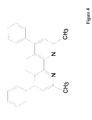
In a representative embodiment of the present invention, the organic electron injection layer comprises 2,9-dimethyl-4,7-diphenyl-1,10-phenanthroline (also called BCP or bathocuproine), which has the structural formula shown in FIG. 4.
One of the advantages of one present invention is that it provides a cathode that may be used in an OLED having a unique combination of high external quantum efficiency and high transparency over the entire visible spectrum.
Another advantage of the invention is that the highly efficient transparent cathode may be used to advantage in other types of optoelectronic devices.
BRIEF DESCRIPTION OF THE DRAWINGS
FIG. 1 shows an OLED, having a compound cathode with a transparent conduction layer 10 a, an exciton blocking layer 10 b, and the remainder of the OLED, 12, wherein the remainder comprises, for example, in sequence, an ETL, an optional separate emitting layer, an HTL, and an anode.
FIG. 2 shows a compound cathode comprising a transparent semiconducting layer, 10 a, an exciton blocking layer, 10 b, and a layer of metal for doping the exciton blocking layer, 10 c.
FIG. 3 shows a compound cathode comprising a transparent semiconducting layer, 10 a, on a layer of metal, 10 c, for doping an exciton blocking layer, 10 b.
FIG. 4 shows the chemical formula for BCP.
FIG. 5 shows the current-density vs. voltage (J-V) plot of OLEDs with the following structure: cathode/Alq3/α-NPD/ITO where the cathode is Mg:Aa, ITO/BCP, TTO/Li/BCP, and ITO/BCP/Li and the Inset shows the total external quantum efficiency (η) vs. current density (J) for these four.
FIG. 6 shows photoluminescence intensity (arbitrary units) vs. wavelength of the following structures grown on quartz: (i) Alq3; (ii) ITO/BCP/Alq3; (iii) ITO/CuPc/Alq3; and (iv) ITO/Alq3.
FIG. 7 shows photoluminescence intensity vs. wavelength of the following structures grown on quartz: (i) Alq3; (ii) BCP/Alq3; (iii) CuPc/BCP/Alq3; and (iv) CuPc/Alq3, with an Inset figure that shows the proposed energy level diagram of the degenerately doped BCP/Li+ layer having a constant Fermi level (EF) at thermal equilibrium and damage states which are due to ITO deposition, and assist in efficient electron injection.
FIG. 8 shows current-density vs. voltage (J-V) characteristics of a Ag/BCP/ITO device. Inset: J-V characteristics of the same device in FIG. 4 with the addition of ˜10 Å of Li at the Ag/BCP interface.
DETAILED DESCRIPTION OF THE PREFERRED EMBODIMENTS OF THE INVENTION
The present invention will now be described in detail for specific preferred embodiments of the invention. These embodiments are intended only as illustrative examples and the invention is not to be limited thereto.
The present invention is directed to a novel cathode comprised of a metal-doped organic electron injection layer that is in direct contact with a transparent, non-metallic, electron injecting cathode layer, such as ITO, wherein the metal-doped organic electron injection layer also functions as an exciton blocking layer and/or as a hole blocking layer. The metal-doped organic electron injection layer is created by diffusing an ultra-thin layer of a highly electropositive metal throughout the layer. Such cathodes may be employed in a wide range of organic optoelectronic devices, such as OLEDs, solar cells, photodetectors, lasers and phototransistors. OLEDs incorporating such cathodes are shown herein to have what are believed to be the highest reported combination of transparency and total device external quantum efficiency for an OLED.
A particular feature of the present invention is the use of an ultra-thin layer of an electropositive metal, such as lithium, which is allowed to diffuse throughout the organic election injection layer that is typically immediately adjacent an electron injecting cathode material such as ITO. An ultra-thin layer refers to a layer that is only of the order of about 5-10 Å thick. Since the electropositive metal can readily diffuse throughout the electron injection layer, the electropositive metal may be deposited on either side or both sides of the electron injection layer.
For example, after preparing a typical sequence of OLED layers, that is, a substrate, an anode, a hold transporting layer (HTL), an optional separate emissive layer, and an electron transporting layer (ETL), the electropositive metal may be deposited as an ultra-thin metal layer directly on the electron transporting layer. The electron injection layer is then deposited on the ultra-thin metal layer. The electron injecting ITO layer would then be deposited on the organic electron injection layer.
Alternatively, he organic electron injection layer may be deposited on the electron transporting layer (ETL), with the electropositive metal layer being thereafter deposited on the organic electron injection layer. In this case, the electron injecting ITO layer is then deposited on the electropositive metal layer.
In each case, it is believed, based on the evidence provided herein, that the electropositive metal diffuses throughout the electron injection layer so as to produce a highly or degenerately doped electron injection layer, in which free electrons are donated to the electron injection layer by the electropositive metal. An electropositive metal refers to a metal that readily loses or gives up electrons, for example, the elements in Groups 1, 2 and 3, or elements in the lanthanide group, of the periodic table. Preferred electropositive metals include, for example, Li, Sr and Sm, with Li being the most preferred electropositive metal.
Since the ultra-thin metal layers are limited to thickness of only about 5-10 Å, it is believed that the electropositive metal diffuses substantially in its entirety into the electron injection layer, such that, after such diffusion, the ultra-thin metallic layer is no longer on the surface of the electron injecting layer. Thus, the entire cathode, which includes both the electron injection ITO layer and the electron injection layer, may be referred to as being non-metallic since the cathode does not contain a separate metallic layer. The metal elements that are present, indium and tin in the ITO layer, are each present in their chemically combined oxide form, whereas the electropositive metals such as lithium are diffused throughout the electron injection layer and, thus, are not present in a metallic form.
The present invention is distinguished from the compound cathodes of U.S. Pat. No. 5,703,436, which include a Mg/Ag layer that typically is of the order of at least about 75-100 Å thick, though layers as thin as 50 Å were disclosed therein. Such compound cathodes, thus, include a separate, but relatively thin, metallic layer. While such compound cathodes were shown to have a sufficiently high transparency such that functional transparent OLEDs could be fabricated, the overall OLED transparency was nevertheless limited by the absorption and reflection losses of the thin metallic layer of the compound cathode. The cathodes of the present invention do not include such a metallic layer. The cathodes of the present invention, thus, do not suffer from the disadvantage of having metallic layers that can cause transparency losses due to absorption and reflection, such as are exhibited by metal layers having a thickness of 50 Å or greater.
It is believed that diffusion of the electropositive metal into the electron injection layer can create a highly degenerately doped layer that enhances election injection into the OLED. More specifically, it is believed that the electropositive material donates electrons to the organic electron injection layer, thereby increasing the conductivity of the electron injection layer to the point that band bonding occurs to aid in the injection of charge into the layer. An increased conductivity results in a reduced barrier for injecting electrons into the electron injection layer, as compared with conventional devices that do not contain an electropositive metal doped in the electron injection layer. A reduction in the electron injection barrier results in a reduced operating voltage for devices that contain the metal doped electron injection layer.
In the representative embodiments of the present invention in which lithium is doped in a BCP layer, it is believed that diffusion of the electropositive lithium metal into the BCP layer creates a highly degenerate metal-doped BCP layer. However, highly doped metal layers that are not doped sufficiently to become fully degenerate are also believed to be capable of functioning within the scope and spirit of the present invention. While it may not be known exactly what fraction of the metal atoms that diffuse into the electron injection layer may contribute to the measurable or charge-carrying electronic density of the layer, the metal atom density in the layer may be selected so as so be sufficient to produce a theoretically expected electronic density, based on the assumption that each metal atom contributes just one charge carrying electron to the molecules in the electron injection layer. For example, based on this assumption, the metal atom density in the layer may be selected so as to produce an electronic density between 1015/cm3 and 1022/cm3. A metal-doped layer according to the present invention, thus, has a metal atom density of at least about 1015/cm3, and preferably a metal atom density of at least about 1021/cm3.
Alternatively, the metal atom density in the electron injection layer can be tailored for producing a total external quantum efficiency greater than the efficiency of an OLED that uses a thick metallic cathode, while also achieving a much greater transparency. More specifically, the metal atom density in the electron injection layer may be selected to be sufficient to produce a total external quantum efficiency of the OLED of at least one percent.
A further feature of the present invention is the use of an exciton blocking and/or a hole blocking material as the organic electron injection layer that is doped with the electropositive metal. By choosing a material that permits the metal-doped organic electron injection layer to function as an exciton blocking layer, the metal-doped organic electron injection layer serves to block diffusion of excitons into the layer, thus allowing more of the excitons within the emission layer to contribute to device efficiency. A material that is used as the exciton blocking layer in an OLED may be defined as a material that has an exciton energy, defined as the energy difference between the electron and hole in a ground state exciton, that is greater than the energy of the excitons that are produced in the emission layer of the OLED. Because of the coulomb forces between the nearby electron and hole in a around state exciton, the exciton energy of an organic material is typically slightly less than the energy difference between the lowest unoccupied molecular orbital (LUMO) and the highest occupied molecular orbital (HOMO) of the material.
By choosing a material that permits the metal-doped organic electron injection layer to function as a hole blocking layer, the metal-doped organic electron injection layer serves to block diffusion of holes into the layer, thus allowing more excitons to be created within the emission layer so as to contribute to a higher device efficiency. The metal-doped organic electron injection, layer, thus, may function as an exciton blocking layer, as a hole blocking layer, or as both an exciton blocking layer and a hole blocking layer.
Since the electron injection layer also has the function of conducting charge carriers, in particular, electrons, the ionization potential (IP) and band gap of the electron injection material are such as to provide efficient charge carrier flow into the adjacent electron transporting layer. The requirements and characteristics of these materials are, thus, as described in the applications having U.S. application Ser. Nos. 09/153,144, filed Sep. 14, 1998, now U.S. Pat. No. 6,097,147, and 09/311,126, filed May 13, 1999, now abandoned, which are incorporated in their entirety by reference.
Furthermore, in each case, an additional layer or layers may be present between one or more of the sequential pairs of these layers. For example, for a double heterostructure, a separate emissive layer is included between the hole transporting layer and the electron transporting layer. This separate emissive layer may be characterized as being a thin luminescent layer. Alternatively, or in addition, a hole injection enhancement layer may be present between the anode layer and the hole transporting layer. In addition, the emissive layer may be comprises of either fluorescent or phosphorescent emission materials.
Thus, while there may be substantial variation in the type, number, thickness and order of the layers that are present, dependent on whether the device includes a single heterostructure or a double heterostructure, whether the device is a SOLED or a single OLED, whether the device is a TOLED or an IOLED, whether the OLED is intended to produce emission in a preferred spectral region, or whether still other design variations are used, the present invention is directed to those devices in which the OLED is comprised of a metal-doped organic electron injection layer that is in direct contact with a transparent, non-metallic, electron injecting cathode layer, such as ITO, wherein the metal-doped organic electron injection layer also functions as an exciton blocking layer and/or as a hole blocking layer.
The cathodes of the present invention may be incorporated into an optoelectronic device that is included in a vehicle, a computer, a television, a printer, a large area wall, theater or stadium screen, a billboard, a laser or a sign, although not limited to only these devices. The devices disclosed in the following patents or co-pending patent applications, each of which is incorporated herein in its entirety, may benefit from incorporation of the non-metallic cathodes of the present invention: U.S. Pat. Nos. 5,703,436; 5,707,745; 5,721,160; 5,757,026; 5,757,139; 5,811,833; 5,834,893; 5,844,363; 5,861,219; 5,874,803; 5,917,280; 5,922,396; 5,932,895; 5,953,587; 5,981,306; 5,986,268; 5,986,401; 5,998,803; 6,005,252; 6,013,538; and 6,013,982; and U.S. patent application Ser. No. 08/779,141, now U.S. Pat. No. 5,986,268; Ser. No. 08/821,380, now U.S. Pat. No. 5,986,401; Ser. No. 08/977,205, now U.S. Pat. No. 6,013,538; Ser. No. 08/865,491, now U.S. Pat. No. 5,998,803; and Der. No. 08/928,800, now U.S. Pat. No. 5,981,306. The materials, methods and apparatus disclosed in these patents and co-pending applications may also be used to prepare the OLEDs of the present invention.
This invention will now be described in detail with respect to showing how certain specific representative embodiments thereof can be made, the materials, apparatus and process steps being understood as examples that are intended to be illustrative only. In particular, the invention is not intended to be limited to the methods, materials, conditions, process parameters, apparatus and the like specifically recited herein.
EXAMPLES OF THE INVENTION
A representative embodiment of the present invention was prepared using a compound cathode comprising 2,9-dimethyl-4,7 diphenyl-1,10-phenanthroline (BCP) as the electron injection layer and inserting an ultra-thin film of about 5-10 Å of lithium (Li), an electropositive metal, into this layer, which was in contact with an electron injecting ITO layer. This compound cathode structure was used in an OLED having a total external quantum efficiency of (1.0±0.05)% at a drive current of 10 mA/cm2, with a transparency of about 90%, or higher, across the entire visible spectrum. This is believed to be the highest reported combination of transparency and total device external quantum efficiency for an OLED. OLEDs having a total external quantum efficiency of at least 1.0% and a transparency of at least 90% are, thus, herein referred to as highly efficient and highly transparent OLEDs.
These results suggest that Li readily diffuses throughout the BCP layer, degenerately doping the BCP. The degenerately doped electron injection layer of BCP acts as an exciton blocking layer, and the Li acts as an electron donor, creating a doped degenerate surface layer to enhance electron injection into the OLED. In one preferred embodiment the degenerate doping of the BCP is controlled leading to an electronic density of at least 1021/cm3. At these densities, the layer of BCP is a degenerate semiconductor which establishes an ohmic contact with the bulk organic semiconductor. See the inset of FIG. 8.
Four sets of transparent, non-metallic OLEDs were fabricated on precleaned and ultraviolet-ozone treated ITO coated glass substrates to positively demonstrate the transparency and efficency benefits of a compound cathode employing an exciton blocking layer. All transparent devices were fabricated without a vacuum break. For purposes of comparison, 650 Å of the hole-transporting layer (HTL) 4,4-bis[N-(1-naphthyl)-N-phenyl-amino] biphenyl ((α-NPD) was vacuum (base pressure of 10−7 Torr) deposited on the ITO, followed by 750 Å of the emissive, electron-transporting layer (ETL): tris-(8-hydroxyquinoline) aluminum (Alq3). A 1500 Å thick Mg:Ag (10:1 mass ratio) cathode followed by a 500 Å cap of Ag was then deposited onto the Alq3 surface through a shadow mask to form the conventional, control OLEDs. Then, three devices including an exciton blocking layer employing the following cathode variations, deposited in reverse sequence: a) ITO/BCP; b) ITO/BCP/Li; and c) ITO/Li/BCP. The thickness of the ITO was about 525 Å, but could have ranged from 100 to 2000 Å. The BCP was about 70 Å, but could have functioned as an effective injection and exciton blocking layer in a range from 20 to 500 Å. The Li layer was about 5-10 Å, but the layer thickness may be varied with the thickness of the BCP layer, such that the lithium produces an electronic density of at least about 1015/cm3, and more preferably at least about 1022/cm3, remaining functional between about 1015/cm3 and 1022/cm3, but not necessarily limited to 1022/cm3, depending on the materials chosen. The ITO was radio-frequency magnetron sputtered from a 10 cm diameter target at a power of 50 W, an Ar flow rate of 140 sccm, and a pressure of 2 mTorr, yielding a deposition rate of 0.3 Å/s. N. Johansson, T. Osada, S. Stafstrom, W. R. Salaneck, V. Parente, D. A. dos Santos, X. Crispin, and J. L Bredas, J. Chem. Phys. 111, 2157 (1999). Elemental Li in the form of a rod was thermally evaporated at a rate of 1 Å/s. However, the cathode could work equally well using other methods of ITO, BCP and lithium deposition. Alternatively, the lithium and BCP may be co-deposited.
The four devices had similar current density-voltage (J-V) characteristics. The graph in FIG. 5 shows two distinct, characteristic regimes for charge transport in small molecule OLEDs: ohmic transport at low drive voltages following J˜V, and trapped-charge limited transport at higher drive voltages following J˜Vm, where m is typically in the range 5-10 at room temperature. G. Parthasarathy, P. E. Burrows, P. Tian, I. G. Hill, A. Kahnr and S. R. Forrest, J. Appl. Phys., 86, 4067 (1999); P. E. Burrows, Z. Shen, V. Bulovic, D. M. McCarty, S. R. Forrest, J. A. Cronin, and M. E. Thompson, J. Appl. Phys. 79, 7991 (1996). The “operation voltage ” is obtained at a current density of 10 mA/cm2, corresponding to a luminance of about 100 cd/m2, the nominal requirement for video applications. Both the Li-containing and Mg:Ag contact devices have similar operating voltages of about 9 V (to within about 1 V). However, the conventional non-metallic device without Li shows a marked increase to 14.5 V. This is believed to be caused by the large injection barrier at the ITO/BCP interface. In all cases, the low voltage regime shows a very low leakage current density of less than or equal to about 10−5 A/cm2, although the Li-free devices had a somewhat higher leakage. Yield, defined as the ratio of non-shorted to the total number of devices tested, for each of the four sets of devices was 100% for a sample size of 16.
The total external quantum efficiencies of the devices are plotted in the inset of FIG. 5. For the transparent devices, the optical output power is the sum of that emitted from both the substrate and the cathode surfaces. At J=10 mA/cm2, the OLED with the metallic cathode had η=(0.85±0.05)% while the transparent devices containing Li had η=(1.0±0.05)%. However, the transparent device without Li shows η=(0.30±0.05)%, consistent with previous unpublished results. Again, this provides evidence of a significant barrier to the transfer of electrons from the conducting layer to the blocking layer or the blocking layer to the device or both, leading to imbalanced injection of charge and thus a lower η.
The insertion of 5-10 Å of Li is known to improve the external quantum efficiency of non-metallic OLEDs. L. S. Hung and C. W. Tang, Appl. Phys. Lett. 74, 3209 (1999). Previous results show that a layer of Li that is too thick causes a reduction in η, ultimately eliminating the benefit achieved by introducing Li into the BCP layer. Therefore, the preferred thickness of the lithium layer falls in an optimum range, which depends on the electronic density of the exciton blocking layer.
In addition, by using BCP, as an exciton blocking layer, and also as a hole blocking layer, instead of CuPc, an increase in the external quantum efficiency of about 40% is shown. This improved efficiency is significant, providing marked improvement in brightness or power consumption.
To make these cathodes useful for integration in full color displays, it is desirable to have high transparency across the entire visible spectrum, thus further motivating the use of a degenerately-doped, exciton blocking, and/or as a hole blocking, cathode instead of CuPc/Li, the latter cathodes being only 65% to 85% transparent in the visible, whereas the cathode with the layer of BCP is about 90% or higher across the entire visible spectrum.
To understand the losses incurred when using CuPc instead of BCP beneath the ITO contact, the relative photoluminescence (PL) efficiencies were measured for the following structures, which were grown on Quartz: (i) Alq3; (ii) ITO/BCP/Alq3; (iii) ITO/CuPc/Alq3; and (iv) ITO/Alq3. The thickness of the Alq3 was 100 Å, the CuPc and BCP was 70 Å, and the ITC cap was 525 Å. A mercury lamp in conjunction with a 10 nm wide optical band pass filter centered at the wavelength of λ=400 nm was used as the excitation source incident via the quartz substrate, creating excitons uniformly throughout the Alq3 layer P. E. Burrows, Z. Shen, V. Eulovic, D. M. McCarty, S. R. Forrest, J. A. Cronin and M. E. Thompson, J. Appl. Phys. 79, 7991 (1996). Further, CuPc is nearly transparent at λ=400 nm, eliminating effects due to exciton generation in that layer. Parthasarathy, P. E. Burrows, V. Khalin. V. G. Kozlov, and S. R. Forrest, Appl. Phys. Lett. 72, 2138 (1998). FIG. 6 shows that the ratio of the PL efficiencies for structures (i):(ii):(iii):(iv) are 16:10:1:1. Since the thicknesses of the organic layers and the ITO were kept constant, and ITO is transparent at the wavelengths studied, microcavity effects do not play a significant role in determining the shape or intensity of the PL spectra in the figure. It may be concluded, therefore that BCP prevents the dramatic quenching of Alq3 excitons due to the sputter induced damage from the ITO at the cathode. S. Parthasarathy, G. Gu and S. R. Forrest, Adv. Mat. 11, 907 (1999). BCP acts effectively in blocking exciton transport to the damaged ITO/organic interface. In contrast, CuPc does not appear to significantly reduce quenching compared to that observed by direct deposition of ITO onto Alq3.
To separate the quenching of Alq3 emission due to the presence of CuPc from that due to the sputter damage under the ITO, the following second set of structures was grown on quartz with the same thicknesses as above: (i) Alq3; (ii) BCP/Alq3; (iii) CuPc/BCP/Alq3; and (iv) CuPc/Alq3. The ratio of the PL efficiencies for structures (i):(ii):(iii):(iv) are 12:10:6:1, as shown In FIG. 7. This shows that CuPc itself quenches Alq3 emission, possibly via exciplex formation at the organic heterostructure interface. In addition, these experiments indicate that BCP, previously shown to be a barrier to Alq3 exciton transport, can be placed between CuPc and Alq3 to partially recover the Alq3 PL intensity by preventing excitons from migrating to the damaged region immediately below the sputtered ITO contact.
It Is known that Li diffuses through organics. E. I. Haskel, A. Curioni, P. F. Seidler and W. Andreoni, Appl. Phys. Lett. 68, 2606 (1997); N. Johansscn, T. Osada, S. Stafstrom, W. R. Salaneck, V. Parente, D. A. dos Santos, X. Crispin and J. L. Bredas, J. Chem. Phys. 111, 2157 (1999). Thus, it is not surprising that placing Li on either side of the BCP layer makes no significant difference in the device characteristics. However, it was reported that the Insertion of Li between CuPc and Alq3 resulted in a substantial increase in the operating voltage when compared to inserting Li between CuPc and the ITO cap. L. S. Hung and C. W. Tang, Appl. Phys. Lett. 74, 3209 (1999). This discrepancy was not observed with the CuPc/Li system. The difference between the present results and the previous results may be attributed to the method of fabrication of the top ITO contact. The present data, combined with the fact that Li acts to improve electron injection, suggests that Li dopes the BCP layer by donating its valence electron, thereby forming Li ions. This doping results in band bending, reducing the barrier to charge injection from the ITO contact into the bulk of the Alq3. Assuming a bulk density of 0.53 g/cm3, 10 Å of Li can donate up to 1016 electrons/cm2 into a layer of BCP of thickness of about 100 Å, leading to an electronic density of about 1021 electrons/cm3. By depositing a thicker continuous layer of Li, the Li atoms are tied to the surface, consequently reducing both diffusion and doping. This explains why Li thicknesses much greater than 10 Å were ineffective in producing high efficiency OLEDs when deposited upon a layer of BCP of about 100 Å.
To test the hypothesis of Li+diffusion and doping, simpler structures of the form: 1500 Å Ag/800 Å BCP/ITO were fabricated with and without about 10 Å Li at the Ag/BCP interface. As shown in FIG. 8, the Li-free device has a rectification ratio of about 105 measured at ±30 V. In contrast, the device containing about 10 Å of Li between the BCP and the Ag shows nearly ohmic behavior at low V, with a contact resistance of about 1 Ω-cm2. This allows for very large currents densities (about 40 A/cm2) at very low voltages (about 2 V) with a rectification ratio of about 1 at ±3.5 V. It may be inferred from these data that Li diffuses throughout the 800 Å BCP layer, degenerately doping the BCP to yield a highly conductive layer air enabling efficient electron injection. N. Johansson, T. Osada, S. Stafstroin, W. R. Salaneck, V. Parente, D. A. dos Santos, X. Crispin and J. L. Bredas, J. Chem. Phys. 111, 2157 (1999). Therefore, BCP degenerately doped with Li is a preferred exciton blocking layer.

Claims (15)

What is claimed is:
1. A highly transparent and highly efficient organic light emitting device comprising, in the following order:
an anode layer comprising ITO;
a hole transporting layer comprising 4,4-bis[N-(1-naphthyl)-N-phenyl-amino]biphenyl;
an electron transporting layer comprising tris-(8-hydroxyquinoline) aluminum; and
a cathode, further comprising a lithium-doped electron injection layer comprising 2,9-dimethyl-4,7-diphenyl-1,10-phenanthroline, and an ITO layer in contact with said lithium-doped electron injection layer.
2. A compound cathode comprising a transparent, non-metallic, electron injecting material in contact with an organic electron injection layer doped with a metal, wherein the organic electron injection layer comprises a transparent organic material that acts as a hole blocking layer, wherein the transparent organic material is 2,9-dimethyl-4,7-diphenyl-1,10-phenanthroline.
3. The compound cathode of claim 2, wherein said metal is selected from the group consisting of Li, Sr and Sm.
4. The compound cathode of claim 2, wherein said metal is Li.
5. The compound cathode of claim 2, wherein said metal produces an electronic density of at least about 1015/cm3.
6. The compound cathode of claim 2, wherein said metal produces an electronic density of at least about 1021/cm3.
7. The compound cathode of claim 2, wherein said transparent, non-metallic, electron injecting material comprises indium tin oxide.
8. The compound cathode of claim 2, wherein said compound cathode is incorporated in an organic optoelectronic device.
9. The compound cathode of claim 8, wherein said optoelectronic device is an organic light emitting device.
10. The compound cathode of claim 9, wherein said organic light emitting device is incorporated in a device selected from the group consisting of a vehicle, a computer, a television, a printer, a screen, a billboard, a display and a telephone.
11. The compound cathode of claim 2, wherein said organic electron injection layer has a thickness of about 20 angstroms to about 500 angstroms.
12. The compound cathode of claim 2, wherein said organic electron injection layer has a thickness of about 70 angstroms.
13. The compound cathode of claim 2, wherein said metal diffuses throughout said organic electron injection layer.
14. A compound cathode comprising a transparent, non-metallic, electron injecting material in contact with an organic electron injection layer comprising 2,9-dimethyl-4,7-diphenyl-1,10-phenanthroline doped with Li.
15. The compound cathode of claim 14, wherein said transparent, non-metallic, electron injecting material comprises indium tin oxide.
US09/522,155 2000-02-28 2000-03-09 High efficiency transparent organic light emitting devices Expired - Fee Related US6639357B1 (en)

Priority Applications (9)

Application Number Priority Date Filing Date Title
US09/522,155 US6639357B1 (en) 2000-02-28 2000-03-09 High efficiency transparent organic light emitting devices
KR1020027011700A KR20020092977A (en) 2000-03-09 2001-03-07 High efficiency transparent organic light emitting devices
EP01914739A EP1281294A1 (en) 2000-03-09 2001-03-07 High efficiency transparent organic light emitting devices
JP2001565709A JP4846953B2 (en) 2000-03-09 2001-03-07 High efficiency transparent organic light emitting device
CNB018074960A CN100438713C (en) 2000-03-09 2001-03-07 High efficiency transparent organic light emitting devices
PCT/US2001/007290 WO2001067825A1 (en) 2000-03-09 2001-03-07 High efficiency transparent organic light emitting devices
AU2001240093A AU2001240093A1 (en) 2000-03-09 2001-03-07 High efficiency transparent organic light emitting devices
TW090105546A TWI231151B (en) 2000-03-09 2001-03-09 High efficiency transparent organic light emitting devices
US10/696,286 US6885149B2 (en) 2000-02-28 2003-10-28 High efficiency transparent organic light emitting devices

Applications Claiming Priority (3)

Application Number Priority Date Filing Date Title
US18523200P 2000-02-28 2000-02-28
US18861300P 2000-03-08 2000-03-08
US09/522,155 US6639357B1 (en) 2000-02-28 2000-03-09 High efficiency transparent organic light emitting devices

Related Parent Applications (1)

Application Number Title Priority Date Filing Date
US09/131,081 Continuation US6149676A (en) 1993-02-10 1998-08-07 Catheter system for controlling a patient's body temperature by in situ blood temperature modification

Related Child Applications (2)

Application Number Title Priority Date Filing Date
US10/004,579 Continuation US6635076B1 (en) 1993-02-10 2001-12-04 System for controlling body temperature of a patient
US10/696,286 Continuation US6885149B2 (en) 2000-02-28 2003-10-28 High efficiency transparent organic light emitting devices

Publications (1)

Publication Number Publication Date
US6639357B1 true US6639357B1 (en) 2003-10-28

Family

ID=24079683

Family Applications (2)

Application Number Title Priority Date Filing Date
US09/522,155 Expired - Fee Related US6639357B1 (en) 2000-02-28 2000-03-09 High efficiency transparent organic light emitting devices
US10/696,286 Expired - Lifetime US6885149B2 (en) 2000-02-28 2003-10-28 High efficiency transparent organic light emitting devices

Family Applications After (1)

Application Number Title Priority Date Filing Date
US10/696,286 Expired - Lifetime US6885149B2 (en) 2000-02-28 2003-10-28 High efficiency transparent organic light emitting devices

Country Status (8)

Country Link
US (2) US6639357B1 (en)
EP (1) EP1281294A1 (en)
JP (1) JP4846953B2 (en)
KR (1) KR20020092977A (en)
CN (1) CN100438713C (en)
AU (1) AU2001240093A1 (en)
TW (1) TWI231151B (en)
WO (1) WO2001067825A1 (en)

Cited By (31)

* Cited by examiner, † Cited by third party
Publication number Priority date Publication date Assignee Title
US20030111666A1 (en) * 2001-11-30 2003-06-19 Semiconductor Energy Laboratory Co., Ltd. Light emitting device
US20030234609A1 (en) * 2001-03-08 2003-12-25 Xerox Corporation Devices with multiple organic-metal mixed layers
US20040161695A1 (en) * 2003-02-14 2004-08-19 Eastman Kodak Company Forming an oled device with a performance-inhancing layer
US6781149B1 (en) * 2003-02-14 2004-08-24 Eastman Kodak Company OLED device with a performance-enhancing layer
US20050195874A1 (en) * 2004-03-05 2005-09-08 Forrest Stephen R. Organic polariton laser
US20050195873A1 (en) * 2004-03-05 2005-09-08 Forrest Stephen R. Organic polariton laser
US20060040131A1 (en) * 2004-08-19 2006-02-23 Eastman Kodak Company OLEDs with improved operational lifetime
US20060046098A1 (en) * 2000-03-27 2006-03-02 Idemitsu Kosan Co., Ltd. Organic electroluminescence element
EP1662591A2 (en) * 2004-11-30 2006-05-31 BenQ Mobile GmbH & Co. oHG An OLED device with double-side Display
US20060133437A1 (en) * 2004-12-21 2006-06-22 Trustees Of Princeton University Organic injection laser
US20060141287A1 (en) * 2004-08-19 2006-06-29 Eastman Kodak Company OLEDs with improved operational lifetime
US20060192484A1 (en) * 2002-08-09 2006-08-31 Semiconductor Energy Laboratory Co., Ltd. Electroluminescence element and a light emitting device using the same
US20070020484A1 (en) * 2005-07-25 2007-01-25 Lg Electronics Inc. Organic electroluminescence device and method for fabricating the same
US20070126347A1 (en) * 2005-12-01 2007-06-07 Eastman Kodak Company OLEDS with improved efficiency
EP1803172A1 (en) * 2004-09-24 2007-07-04 Semiconductor Energy Laboratory Co., Ltd. Light emitting device
US20070206156A1 (en) * 2006-03-03 2007-09-06 Quach Cang V One-way transparent display systems
WO2007099229A2 (en) 2006-02-28 2007-09-07 Commissariat A L'energie Atomique Electronic component comprising a p-doped organic semiconductor
US20070241663A1 (en) * 2006-04-12 2007-10-18 Toppoly Optoelectronics Corp. Organic electroluminescent device
US20070252516A1 (en) * 2006-04-27 2007-11-01 Eastman Kodak Company Electroluminescent devices including organic EIL layer
US20080018233A1 (en) * 2005-04-15 2008-01-24 Vardeny Zeev V Perforated-electrode organic light-emitting diodes
US20080174735A1 (en) * 2007-01-23 2008-07-24 Emiscape, Inc. Projection Display with Holographic Screen
WO2009040724A2 (en) 2007-09-26 2009-04-02 Philips Intellectual Property & Standards Gmbh Window system combining window and illumination functionalities
US20090206747A1 (en) * 2005-03-25 2009-08-20 Shi-Hao Li Organic Electro-Luminescence Device
US20100084647A1 (en) * 2006-04-27 2010-04-08 Kondakova Marina E Electroluminescent devices including organic eil layer
US20100215838A1 (en) * 2006-04-12 2010-08-26 Chi-Hsien Huang Method of manufacturing organic electroluminescent device
US7943244B2 (en) 2005-05-20 2011-05-17 Lg Display Co., Ltd. Display device with metal-organic mixed layer anodes
US20110186864A1 (en) * 2006-01-11 2011-08-04 Novaled Ag Electroluminescent light-emitting device comprising an arrangement of organic layers, and method for its production
US8487527B2 (en) 2005-05-04 2013-07-16 Lg Display Co., Ltd. Organic light emitting devices
CN107170898A (en) * 2017-05-11 2017-09-15 安徽熙泰智能科技有限公司 One kind is inverted OLED
US10693102B2 (en) 2017-09-15 2020-06-23 Industrial Technology Research Institute Light emitting device and transparent electrode thereof, and transparent light emitting device having a light-transmitting area and a light-opaque area
US11733540B2 (en) 2019-10-01 2023-08-22 Industrial Technology Research Institute Space three-dimensional imaging apparatus and method

Families Citing this family (35)

* Cited by examiner, † Cited by third party
Publication number Priority date Publication date Assignee Title
KR100483988B1 (en) 2001-11-29 2005-04-15 삼성에스디아이 주식회사 Method of Varying Transmittance in transparent conductive film
US20100026176A1 (en) 2002-03-28 2010-02-04 Jan Blochwitz-Nomith Transparent, Thermally Stable Light-Emitting Component Having Organic Layers
DE10215210B4 (en) * 2002-03-28 2006-07-13 Novaled Gmbh Transparent, thermally stable light-emitting component with organic layers
US6642092B1 (en) 2002-07-11 2003-11-04 Sharp Laboratories Of America, Inc. Thin-film transistors formed on a metal foil substrate
TW554641B (en) * 2002-08-19 2003-09-21 Univ Nat Taiwan Manufacturing method of organic graded junction
TW578439B (en) * 2002-10-25 2004-03-01 Ritdisplay Corp Organic light emitting diode and material applied in the organic light emitting diode
KR100560785B1 (en) 2003-02-03 2006-03-13 삼성에스디아이 주식회사 Organic electroluminecent display device driven by low voltage
US7675057B2 (en) * 2003-03-19 2010-03-09 Technische Universitaet Dresden Photoactive component with organic layers
US6703180B1 (en) * 2003-04-16 2004-03-09 Eastman Kodak Company Forming an improved stability emissive layer from a donor element in an OLED device
US7514159B2 (en) 2003-06-13 2009-04-07 Semiconductor Energy Laboratory Co., Ltd. Electron injection composition for light emitting element, light emitting element, and light emitting device
KR100527194B1 (en) 2003-06-24 2005-11-08 삼성에스디아이 주식회사 organic electroluminescence device employing doped hole transfer layer and/or hole injection layer
DE10339772B4 (en) 2003-08-27 2006-07-13 Novaled Gmbh Light emitting device and method for its production
US7138763B2 (en) * 2003-11-14 2006-11-21 Eastman Kodak Company Organic electroluminescent devices having a stability-enhancing layer
CN100431194C (en) * 2004-10-18 2008-11-05 财团法人工业技术研究院 Cathode structure for inversion type organic luminous assembly
TWI471058B (en) * 2005-06-01 2015-01-21 Univ Princeton Fluorescent filtered electrophosphorescence
US7474048B2 (en) * 2005-06-01 2009-01-06 The Trustees Of Princeton University Fluorescent filtered electrophosphorescence
WO2006129265A2 (en) * 2005-06-03 2006-12-07 Philips Intellectual Property & Standards Gmbh Organic electroluminescent light source
JP2007059783A (en) * 2005-08-26 2007-03-08 Showa Denko Kk Organic el device, method for manufacturing the same and application thereof
US20070128465A1 (en) * 2005-12-05 2007-06-07 General Electric Company Transparent electrode for organic electronic devices
CN101400757B (en) 2006-03-14 2013-05-15 Lg化学株式会社 Organic light emitting diode having high efficiency and process for fabricating the same
GB2440368A (en) * 2006-07-26 2008-01-30 Oled T Ltd Cathode coating for an electroluminescent device
US7710017B2 (en) * 2006-09-08 2010-05-04 Universal Display Corporation Organic light emitting device having a transparent microcavity
US7800295B2 (en) * 2006-09-15 2010-09-21 Universal Display Corporation Organic light emitting device having a microcavity
GB0625865D0 (en) * 2006-12-29 2007-02-07 Oled T Ltd Electro-optical or opto-electronic device
US7728512B2 (en) * 2007-03-02 2010-06-01 Universal Display Corporation Organic light emitting device having an external microcavity
US8076009B2 (en) * 2007-10-26 2011-12-13 Global Oled Technology, Llc. OLED device with fluoranthene electron transport materials
CA2740988A1 (en) * 2008-10-17 2010-04-22 Bloominescence Llc Transparent polarized light-emitting device
US8637331B2 (en) 2008-10-17 2014-01-28 Bloominescence, Llc Transparent polarized light-emitting device
CN102273320B (en) 2008-11-13 2014-12-03 株式会社Lg化学 Low voltage-driven organic electroluminescence device, and manufacturing method thereof
KR101148886B1 (en) * 2009-05-13 2012-05-29 네오뷰코오롱 주식회사 Organic light emitting diode and manufacturing method thereof
TW201144406A (en) * 2010-01-15 2011-12-16 Idemitsu Kosan Co Organic electroluminescent element
CN109192868B (en) * 2018-08-10 2020-07-03 深圳市华星光电半导体显示技术有限公司 Transparent conductive film, display panel and display device
CN109755402B (en) * 2019-01-10 2021-01-05 云谷(固安)科技有限公司 Display panel and display device
CN109839746A (en) * 2019-03-05 2019-06-04 京东方科技集团股份有限公司 A kind of near-eye display device and preparation method thereof
CN112802974A (en) * 2020-12-30 2021-05-14 广东聚华印刷显示技术有限公司 Electronic device structure, preparation method thereof, light emitting diode and display device

Citations (41)

* Cited by examiner, † Cited by third party
Publication number Priority date Publication date Assignee Title
US4164431A (en) 1977-08-02 1979-08-14 Eastman Kodak Company Multilayer organic photovoltaic elements
US4611385A (en) 1982-06-18 1986-09-16 At&T Bell Laboratories Devices formed utilizing organic materials
US4720432A (en) 1987-02-11 1988-01-19 Eastman Kodak Company Electroluminescent device with organic luminescent medium
US5047687A (en) 1990-07-26 1991-09-10 Eastman Kodak Company Organic electroluminescent device with stabilized cathode
US5059862A (en) 1990-07-26 1991-10-22 Eastman Kodak Company Electroluminescent device with improved cathode
US5315129A (en) 1990-08-20 1994-05-24 University Of Southern California Organic optoelectronic devices and methods
US5399936A (en) 1992-04-30 1995-03-21 Pioneer Electronic Corporation Organic electroluminescent device
US5554220A (en) 1995-05-19 1996-09-10 The Trustees Of Princeton University Method and apparatus using organic vapor phase deposition for the growth of organic thin films with large optical non-linearities
WO1997033296A1 (en) 1996-03-06 1997-09-12 The Trustees Of Princeton University Transparent contacts for organic devices
US5677572A (en) 1996-07-29 1997-10-14 Eastman Kodak Company Bilayer electrode on a n-type semiconductor
US5707745A (en) 1994-12-13 1998-01-13 The Trustees Of Princeton University Multicolor organic light emitting devices
US5714838A (en) 1996-09-20 1998-02-03 International Business Machines Corporation Optically transparent diffusion barrier and top electrode in organic light emitting diode structures
JPH1050481A (en) * 1996-07-31 1998-02-20 Pioneer Electron Corp Organic electroluminescent element
US5739635A (en) 1995-04-27 1998-04-14 Pioneer Electric Corporation Organic electroluminescent device
US5757139A (en) 1997-02-03 1998-05-26 The Trustees Of Princeton University Driving circuit for stacked organic light emitting devices
US5776623A (en) 1996-07-29 1998-07-07 Eastman Kodak Company Transparent electron-injecting electrode for use in an electroluminescent device
US5776622A (en) 1996-07-29 1998-07-07 Eastman Kodak Company Bilayer eletron-injeting electrode for use in an electroluminescent device
US5811833A (en) 1996-12-23 1998-09-22 University Of So. Ca Electron transporting and light emitting layers based on organic free radicals
US5834893A (en) 1996-12-23 1998-11-10 The Trustees Of Princeton University High efficiency organic light emitting devices with light directing structures
US5844363A (en) 1997-01-23 1998-12-01 The Trustees Of Princeton Univ. Vacuum deposited, non-polymeric flexible organic light emitting devices
US5861219A (en) 1997-04-15 1999-01-19 The Trustees Of Princeton University Organic light emitting devices containing a metal complex of 5-hydroxy-quinoxaline as a host material
US5874803A (en) 1997-09-09 1999-02-23 The Trustees Of Princeton University Light emitting device with stack of OLEDS and phosphor downconverter
US5917280A (en) 1997-02-03 1999-06-29 The Trustees Of Princeton University Stacked organic light emitting devices
US5932895A (en) 1997-05-20 1999-08-03 The Trustees Of Princeton University Saturated full color stacked organic light emitting devices
US5937272A (en) 1997-06-06 1999-08-10 Eastman Kodak Company Patterned organic layers in a full-color organic electroluminescent display array on a thin film transistor array substrate
US5953587A (en) 1997-11-24 1999-09-14 The Trustees Of Princeton University Method for deposition and patterning of organic thin film
US5981306A (en) 1997-09-12 1999-11-09 The Trustees Of Princeton University Method for depositing indium tin oxide layers in organic light emitting devices
US5986268A (en) 1996-01-11 1999-11-16 The Trustees Of Princeton University Organic luminescent coating for light detectors
US5986401A (en) 1997-03-20 1999-11-16 The Trustee Of Princeton University High contrast transparent organic light emitting device display
US5998803A (en) 1997-05-29 1999-12-07 The Trustees Of Princeton University Organic light emitting device containing a hole injection enhancement layer
US6010796A (en) * 1996-07-09 2000-01-04 Sony Corporation Electroluminescent device
US6013384A (en) 1997-01-27 2000-01-11 Junji Kido Organic electroluminescent devices
US6013982A (en) 1996-12-23 2000-01-11 The Trustees Of Princeton University Multicolor display devices
US6013538A (en) 1997-11-24 2000-01-11 The Trustees Of Princeton University Method of fabricating and patterning OLEDs
US6064151A (en) 1997-12-08 2000-05-16 Motorola, Inc. Organic electroluminescent device with enhanced performance
US6069442A (en) 1997-09-18 2000-05-30 Eastman Kodak Company Organic electroluminescent device with inorganic electron transporting layer
US6137223A (en) * 1998-07-28 2000-10-24 Eastman Kodak Company Electron-injecting layer formed from a dopant layer for organic light-emitting structure
US6140763A (en) 1998-07-28 2000-10-31 Eastman Kodak Company Interfacial electron-injecting layer formed from a doped cathode for organic light-emitting structure
US6172459B1 (en) 1998-07-28 2001-01-09 Eastman Kodak Company Electron-injecting layer providing a modified interface between an organic light-emitting structure and a cathode buffer layer
EP1076368A2 (en) 1999-08-11 2001-02-14 Eastman Kodak Company A surface-emitting organic light-emitting diode
US6278236B1 (en) 1999-09-02 2001-08-21 Eastman Kodak Company Organic electroluminescent devices with electron-injecting layer having aluminum and alkali halide

Family Cites Families (10)

* Cited by examiner, † Cited by third party
Publication number Priority date Publication date Assignee Title
US5108369A (en) * 1990-03-15 1992-04-28 Diagnostic Devices Group, Limited Dual-diameter multifunction catheter
JP3562652B2 (en) * 1992-04-03 2004-09-08 パイオニア株式会社 Organic electroluminescence device
ATE247372T1 (en) * 1996-09-04 2003-08-15 Cambridge Display Tech Ltd LIGHT EMITTING ORGANIC DEVICES WITH IMPROVED CATHODE
JPH10162959A (en) * 1996-11-29 1998-06-19 Idemitsu Kosan Co Ltd Organic electro-luminescence element
JPH11102786A (en) * 1997-09-29 1999-04-13 Minolta Co Ltd Organic electroluminescence element
JP3496537B2 (en) * 1997-10-17 2004-02-16 東レ株式会社 Organic electroluminescent device
JPH11354280A (en) * 1998-04-10 1999-12-24 Toray Ind Inc Light-emitting device
US6451415B1 (en) * 1998-08-19 2002-09-17 The Trustees Of Princeton University Organic photosensitive optoelectronic device with an exciton blocking layer
US6097147A (en) * 1998-09-14 2000-08-01 The Trustees Of Princeton University Structure for high efficiency electroluminescent device
US6366017B1 (en) * 1999-07-14 2002-04-02 Agilent Technologies, Inc/ Organic light emitting diodes with distributed bragg reflector

Patent Citations (47)

* Cited by examiner, † Cited by third party
Publication number Priority date Publication date Assignee Title
US4164431A (en) 1977-08-02 1979-08-14 Eastman Kodak Company Multilayer organic photovoltaic elements
US4611385A (en) 1982-06-18 1986-09-16 At&T Bell Laboratories Devices formed utilizing organic materials
US4720432A (en) 1987-02-11 1988-01-19 Eastman Kodak Company Electroluminescent device with organic luminescent medium
US5047687A (en) 1990-07-26 1991-09-10 Eastman Kodak Company Organic electroluminescent device with stabilized cathode
US5059862A (en) 1990-07-26 1991-10-22 Eastman Kodak Company Electroluminescent device with improved cathode
US5315129A (en) 1990-08-20 1994-05-24 University Of Southern California Organic optoelectronic devices and methods
US5399936A (en) 1992-04-30 1995-03-21 Pioneer Electronic Corporation Organic electroluminescent device
US5757026A (en) 1994-12-13 1998-05-26 The Trustees Of Princeton University Multicolor organic light emitting devices
US5703436A (en) 1994-12-13 1997-12-30 The Trustees Of Princeton University Transparent contacts for organic devices
US5707745A (en) 1994-12-13 1998-01-13 The Trustees Of Princeton University Multicolor organic light emitting devices
US5721160A (en) 1994-12-13 1998-02-24 The Trustees Of Princeton University Multicolor organic light emitting devices
US5739635A (en) 1995-04-27 1998-04-14 Pioneer Electric Corporation Organic electroluminescent device
US5554220A (en) 1995-05-19 1996-09-10 The Trustees Of Princeton University Method and apparatus using organic vapor phase deposition for the growth of organic thin films with large optical non-linearities
US6005252A (en) 1996-01-11 1999-12-21 The Trustees Of Princeton University Method and apparatus for measuring film spectral properties
US5986268A (en) 1996-01-11 1999-11-16 The Trustees Of Princeton University Organic luminescent coating for light detectors
WO1997033296A1 (en) 1996-03-06 1997-09-12 The Trustees Of Princeton University Transparent contacts for organic devices
US6010796A (en) * 1996-07-09 2000-01-04 Sony Corporation Electroluminescent device
US5776623A (en) 1996-07-29 1998-07-07 Eastman Kodak Company Transparent electron-injecting electrode for use in an electroluminescent device
US5776622A (en) 1996-07-29 1998-07-07 Eastman Kodak Company Bilayer eletron-injeting electrode for use in an electroluminescent device
US5677572A (en) 1996-07-29 1997-10-14 Eastman Kodak Company Bilayer electrode on a n-type semiconductor
US5949186A (en) 1996-07-31 1999-09-07 Pioneer Electronic Corporation Organic electroluminescent element
JPH1050481A (en) * 1996-07-31 1998-02-20 Pioneer Electron Corp Organic electroluminescent element
US5714838A (en) 1996-09-20 1998-02-03 International Business Machines Corporation Optically transparent diffusion barrier and top electrode in organic light emitting diode structures
US5811833A (en) 1996-12-23 1998-09-22 University Of So. Ca Electron transporting and light emitting layers based on organic free radicals
US5834893A (en) 1996-12-23 1998-11-10 The Trustees Of Princeton University High efficiency organic light emitting devices with light directing structures
US6013982A (en) 1996-12-23 2000-01-11 The Trustees Of Princeton University Multicolor display devices
US5922396A (en) 1996-12-23 1999-07-13 The University Of Southern California Electron transporting and light emitting layers based on organic free radicals
US5844363A (en) 1997-01-23 1998-12-01 The Trustees Of Princeton Univ. Vacuum deposited, non-polymeric flexible organic light emitting devices
US6013384A (en) 1997-01-27 2000-01-11 Junji Kido Organic electroluminescent devices
US5917280A (en) 1997-02-03 1999-06-29 The Trustees Of Princeton University Stacked organic light emitting devices
US5757139A (en) 1997-02-03 1998-05-26 The Trustees Of Princeton University Driving circuit for stacked organic light emitting devices
US5986401A (en) 1997-03-20 1999-11-16 The Trustee Of Princeton University High contrast transparent organic light emitting device display
US5861219A (en) 1997-04-15 1999-01-19 The Trustees Of Princeton University Organic light emitting devices containing a metal complex of 5-hydroxy-quinoxaline as a host material
US5932895A (en) 1997-05-20 1999-08-03 The Trustees Of Princeton University Saturated full color stacked organic light emitting devices
US5998803A (en) 1997-05-29 1999-12-07 The Trustees Of Princeton University Organic light emitting device containing a hole injection enhancement layer
US5937272A (en) 1997-06-06 1999-08-10 Eastman Kodak Company Patterned organic layers in a full-color organic electroluminescent display array on a thin film transistor array substrate
US5874803A (en) 1997-09-09 1999-02-23 The Trustees Of Princeton University Light emitting device with stack of OLEDS and phosphor downconverter
US5981306A (en) 1997-09-12 1999-11-09 The Trustees Of Princeton University Method for depositing indium tin oxide layers in organic light emitting devices
US6069442A (en) 1997-09-18 2000-05-30 Eastman Kodak Company Organic electroluminescent device with inorganic electron transporting layer
US6013538A (en) 1997-11-24 2000-01-11 The Trustees Of Princeton University Method of fabricating and patterning OLEDs
US5953587A (en) 1997-11-24 1999-09-14 The Trustees Of Princeton University Method for deposition and patterning of organic thin film
US6064151A (en) 1997-12-08 2000-05-16 Motorola, Inc. Organic electroluminescent device with enhanced performance
US6137223A (en) * 1998-07-28 2000-10-24 Eastman Kodak Company Electron-injecting layer formed from a dopant layer for organic light-emitting structure
US6140763A (en) 1998-07-28 2000-10-31 Eastman Kodak Company Interfacial electron-injecting layer formed from a doped cathode for organic light-emitting structure
US6172459B1 (en) 1998-07-28 2001-01-09 Eastman Kodak Company Electron-injecting layer providing a modified interface between an organic light-emitting structure and a cathode buffer layer
EP1076368A2 (en) 1999-08-11 2001-02-14 Eastman Kodak Company A surface-emitting organic light-emitting diode
US6278236B1 (en) 1999-09-02 2001-08-21 Eastman Kodak Company Organic electroluminescent devices with electron-injecting layer having aluminum and alkali halide

Non-Patent Citations (22)

* Cited by examiner, † Cited by third party
Title
Bulovic, et al., "Study of locilized and extended excitons in 3,4,9,10-perylenetetracarboxylic dianhydride (PTCDA) . . . ," Chem. Phys. 210 (1996) pp. 1-12. (No month).
C.W. Tang, et al., "Organic Electroluminescent Diodes", 51 Appl. Phys. Lett., 913 (1987). (Sep.).
Co-pending application Ser. No. 09/153,144, filed Sep. 14, 1998, entitled "Structure for High Efficiency Electroluminescent Device". (Now U.S. patent no. 6,097,147).
E.I. Haskal, et al., "Lithium-aluminum contacts for organic-light emitting devices", Appl. Phys. Lett., 71, pp. 1151-1153 (Sep. 1, 1997).
Forrest, et al., "Organic-on-inorganic semiconductor contact barrier diodes . . . ," J. Appl. Phys. 56 (1984) pp. 543. (Jul.).
G. Gu, et al., "Transparent stacked organic light emitting devices", J. Appl. Phys., 86, pp. 4067-4075 (1999). (Oct.).
G. Parthasarathy, et al., "A full color transparent metal-free stacked organic light emitting device with simplified pixel biasing", Adv. Mat. , 11, pp. 907-910 (1999). (No month).
G. Parthasarathy, et al.,"Metal-free cathode for organic semiconductor devices", Appl. Phys. Lett., 72, pp. 2138-2140 (1998). (Apr.).
Hung, et al., "Enhanced electron injection in organic electroluminescence devices using an Al/LiF electrode," Appl. Phys. Lett. 70 (1997) pp. 152. (Jan.).
J. Kido, et al., "Bright organic electroluminescent devices having a metal-doped electron-injecting layer", Applied Physics Letters, v. 73, n.20, pp. 2866-2868 (1998). (Nov.).
Kido and K. Nagai, "Organic Electroluminescent Devices Using Lanthanide Complexes," Journal of Alloys and Compounds, vol. 192 (1993) pp. 30-33. (No month).
Kido, et al., "Bright red light-emitting organic electroluminescent devices having a europium complex as an emitter," Appl. Phys. Lett., v.65 (1994) pp. 2124-2126. (Oct.).
Kido, et al., "Electroluminescence in terbium complex," Chemistry Letters (1990) pp. 657-660. (No month).
Kido, et al., "Multilayer white light-emitting organic electroluminescent device," Science, v.267 (1995) pp. 1332. (Mar.).
Kido, et al., "White-light-emitting organic electroluminescent device using lanthanide complexes," Jpn. J. Appl. Phys., v.35 (1996) pp. L394-L396. (Mar.).
L.S. Hung, et al., "Interface engineering in preparation of organic surface-emitting diodes", Applied Physics Letters, v.74, n.21, pp. 3209-3211 (1999). (May).
N. Johansson, et al., "Electronic structure of tris (8-hydroxyquinoline) aluminum thin films in the pristine and reduced states", J. Chem. Phys., 111, pp. 2157-2163 (1999). (Aug.).
P. E. Burrows, et al., "Relationship between electroluminescence and current transport in organic heterojunction light-emitting devices", J. Appl. Phys. ,79, pp. 7991-8006 (1996). (May).
Parthasarathy, et al., "A Highly Transparent Organic Light Emitting Device Employing a Metal-Free Cathode," Poster Session Abstract, Materials Research Fair, Princeton Materials Institute, Princeton University (Nov. 6, 1997).
S.R. Forrest, et al., "Organic Emitters Promise a New Generation of Displays", Laser Focus World, (Feb. 1995).
V. Bulovic, et al.,"Transparent light-emitting devices" Nature, 380, p. 29 (1996). (Mar.).
Z. Shen, et al. "Three-Color, Tunable, Organic Light-Emitting Devices", Science, 276, pp. 2009-2011 (1997). (Jun.).

Cited By (64)

* Cited by examiner, † Cited by third party
Publication number Priority date Publication date Assignee Title
US7226546B2 (en) * 2000-03-27 2007-06-05 Idemitsu Kosan Co., Ltd. Organic electroluminescence element
US20060046098A1 (en) * 2000-03-27 2006-03-02 Idemitsu Kosan Co., Ltd. Organic electroluminescence element
US20110163660A1 (en) * 2000-03-27 2011-07-07 Idemitsu Kosan Co., Ltd. Organic electroluminescence element
US8753757B2 (en) 2000-03-27 2014-06-17 Idemitsu Kosan Co., Ltd. Organic electroluminescence element
US7288887B2 (en) * 2001-03-08 2007-10-30 Lg.Philips Lcd Co. Ltd. Devices with multiple organic-metal mixed layers
US20030234609A1 (en) * 2001-03-08 2003-12-25 Xerox Corporation Devices with multiple organic-metal mixed layers
US7868324B2 (en) 2001-11-30 2011-01-11 Semiconductor Energy Laboratory Co., Ltd. Light emitting device
US20110108817A1 (en) * 2001-11-30 2011-05-12 Semiconductor Energy Laboratory Co., Ltd. Light Emitting Device
US20070063196A1 (en) * 2001-11-30 2007-03-22 Semiconductor Energy Laboratory Co., Ltd. Light emitting device
US20080278069A1 (en) * 2001-11-30 2008-11-13 Semiconductor Energy Laboratory Co., Ltd. Light Emitting Device
US7372076B2 (en) 2001-11-30 2008-05-13 Semiconductor Energy Laboratory Co., Ltd. Light emitting device
US8338824B2 (en) 2001-11-30 2012-12-25 Semiconductor Energy Laboratory Co., Ltd. Light emitting device
US8610142B2 (en) 2001-11-30 2013-12-17 Semiconductor Energy Laboratory Co., Ltd. Light emitting device
US7141817B2 (en) * 2001-11-30 2006-11-28 Semiconductor Energy Laboratory Co., Ltd. Light emitting device
US20030111666A1 (en) * 2001-11-30 2003-06-19 Semiconductor Energy Laboratory Co., Ltd. Light emitting device
US20060192484A1 (en) * 2002-08-09 2006-08-31 Semiconductor Energy Laboratory Co., Ltd. Electroluminescence element and a light emitting device using the same
US7737630B2 (en) 2002-08-09 2010-06-15 Semiconductor Energy Laboratory Co., Ltd. Electroluminescence element and a light emitting device using the same
US6824950B2 (en) * 2003-02-14 2004-11-30 Eastman Kodak Company Forming an oled device with a performance-inhancing layer
US20040161695A1 (en) * 2003-02-14 2004-08-19 Eastman Kodak Company Forming an oled device with a performance-inhancing layer
US6781149B1 (en) * 2003-02-14 2004-08-24 Eastman Kodak Company OLED device with a performance-enhancing layer
US7889774B2 (en) 2004-03-05 2011-02-15 The Trustees Of Princeton University Organic polariton laser
US20050195874A1 (en) * 2004-03-05 2005-09-08 Forrest Stephen R. Organic polariton laser
US20050195873A1 (en) * 2004-03-05 2005-09-08 Forrest Stephen R. Organic polariton laser
US20060141287A1 (en) * 2004-08-19 2006-06-29 Eastman Kodak Company OLEDs with improved operational lifetime
US20060040131A1 (en) * 2004-08-19 2006-02-23 Eastman Kodak Company OLEDs with improved operational lifetime
US8643003B2 (en) 2004-09-24 2014-02-04 Semiconductor Energy Laboratory Co., Ltd. Light emitting device
EP1803172A1 (en) * 2004-09-24 2007-07-04 Semiconductor Energy Laboratory Co., Ltd. Light emitting device
EP1803172B1 (en) * 2004-09-24 2017-10-25 Semiconductor Energy Laboratory Co., Ltd. Light emitting device
EP1662591A2 (en) * 2004-11-30 2006-05-31 BenQ Mobile GmbH & Co. oHG An OLED device with double-side Display
EP1662591A3 (en) * 2004-11-30 2010-06-02 Palm, Inc. An OLED device with double-side Display
US7242703B2 (en) * 2004-12-21 2007-07-10 The Trustees Of Princeton University Organic injection laser
US20060133437A1 (en) * 2004-12-21 2006-06-22 Trustees Of Princeton University Organic injection laser
US20090206747A1 (en) * 2005-03-25 2009-08-20 Shi-Hao Li Organic Electro-Luminescence Device
US7938936B2 (en) * 2005-03-25 2011-05-10 Au Optronics Corp. Organic electro-luminescence device
US20110175075A1 (en) * 2005-03-25 2011-07-21 Au Optronics Corp. Organic Electro-Luminescence Device
US8686627B2 (en) * 2005-04-15 2014-04-01 University Of Utah Research Foundation Perforated-electrode organic light-emitting diodes
US20080018233A1 (en) * 2005-04-15 2008-01-24 Vardeny Zeev V Perforated-electrode organic light-emitting diodes
US8487527B2 (en) 2005-05-04 2013-07-16 Lg Display Co., Ltd. Organic light emitting devices
US7943244B2 (en) 2005-05-20 2011-05-17 Lg Display Co., Ltd. Display device with metal-organic mixed layer anodes
US8563144B2 (en) * 2005-07-25 2013-10-22 Lg Display Co., Ltd. Organic electroluminescence device and method for fabricating the same
US20070020484A1 (en) * 2005-07-25 2007-01-25 Lg Electronics Inc. Organic electroluminescence device and method for fabricating the same
US20070126347A1 (en) * 2005-12-01 2007-06-07 Eastman Kodak Company OLEDS with improved efficiency
US8502200B2 (en) 2006-01-11 2013-08-06 Novaled Ag Electroluminescent light-emitting device comprising an arrangement of organic layers, and method for its production
US20110186864A1 (en) * 2006-01-11 2011-08-04 Novaled Ag Electroluminescent light-emitting device comprising an arrangement of organic layers, and method for its production
EP1808910B1 (en) * 2006-01-11 2011-11-16 Novaled AG Electronic component with at least one organic layer
WO2007099229A2 (en) 2006-02-28 2007-09-07 Commissariat A L'energie Atomique Electronic component comprising a p-doped organic semiconductor
US20090015154A1 (en) * 2006-02-28 2009-01-15 Commissariat A L'energie Atomique Electronic Component With P-Doped Organic Semiconductor
US8294359B2 (en) 2006-02-28 2012-10-23 Commissariat A L'energie Atomique Electronic component with p-doped organic semiconductor
US8104895B2 (en) 2006-03-03 2012-01-31 Quach Cang V One-way transparent display systems
US7854513B2 (en) 2006-03-03 2010-12-21 Quach Cang V One-way transparent display systems
US20070206156A1 (en) * 2006-03-03 2007-09-06 Quach Cang V One-way transparent display systems
US20110057212A1 (en) * 2006-03-03 2011-03-10 Quach Cang V One-Way Transparent Display Systems
US20070241663A1 (en) * 2006-04-12 2007-10-18 Toppoly Optoelectronics Corp. Organic electroluminescent device
US20100215838A1 (en) * 2006-04-12 2010-08-26 Chi-Hsien Huang Method of manufacturing organic electroluminescent device
US20070252516A1 (en) * 2006-04-27 2007-11-01 Eastman Kodak Company Electroluminescent devices including organic EIL layer
US20100084647A1 (en) * 2006-04-27 2010-04-08 Kondakova Marina E Electroluminescent devices including organic eil layer
US9118020B2 (en) 2006-04-27 2015-08-25 Global Oled Technology Llc Electroluminescent devices including organic eil layer
US20150311447A1 (en) * 2006-04-27 2015-10-29 Global Oled Technology Llc Electroluminescent devices including organic eil layer
US9634256B2 (en) * 2006-04-27 2017-04-25 Global Oled Technology Llc Electroluminescent devices including organic EIL layer
US20080174735A1 (en) * 2007-01-23 2008-07-24 Emiscape, Inc. Projection Display with Holographic Screen
WO2009040724A2 (en) 2007-09-26 2009-04-02 Philips Intellectual Property & Standards Gmbh Window system combining window and illumination functionalities
CN107170898A (en) * 2017-05-11 2017-09-15 安徽熙泰智能科技有限公司 One kind is inverted OLED
US10693102B2 (en) 2017-09-15 2020-06-23 Industrial Technology Research Institute Light emitting device and transparent electrode thereof, and transparent light emitting device having a light-transmitting area and a light-opaque area
US11733540B2 (en) 2019-10-01 2023-08-22 Industrial Technology Research Institute Space three-dimensional imaging apparatus and method

Also Published As

Publication number Publication date
CN100438713C (en) 2008-11-26
JP4846953B2 (en) 2011-12-28
CN1421115A (en) 2003-05-28
JP2003526188A (en) 2003-09-02
EP1281294A1 (en) 2003-02-05
WO2001067825A1 (en) 2001-09-13
US6885149B2 (en) 2005-04-26
KR20020092977A (en) 2002-12-12
TWI231151B (en) 2005-04-11
US20040085016A1 (en) 2004-05-06
AU2001240093A1 (en) 2001-09-17

Similar Documents

Publication Publication Date Title
US6639357B1 (en) High efficiency transparent organic light emitting devices
US7563519B2 (en) OLEDs doped with phosphorescent compounds
US6469437B1 (en) Highly transparent organic light emitting device employing a non-metallic cathode
US5811833A (en) Electron transporting and light emitting layers based on organic free radicals
Ikai et al. Highly efficient phosphorescence from organic light-emitting devices with an exciton-block layer
JP3992929B2 (en) High-efficiency organic light-emitting device based on electrophosphorescence
KR101026514B1 (en) Organic light emitting devices
US6451455B1 (en) Metal complexes bearing both electron transporting and hole transporting moieties
Chang et al. High-efficiency organic electroluminescent device with multiple emitting units
JP3852552B2 (en) Organic electroluminescence device
US20030230980A1 (en) Very low voltage, high efficiency phosphorescent oled in a p-i-n structure
Parthasarathy et al. High-efficiency transparent organic light-emitting devices
JP2002100482A (en) Organic electroluminescence element
JP2009147364A (en) Double doped-layer, phosphorescent organic light-emitting device
JP2011082564A (en) Oled having non-hole blocking buffer layer
JP2004515895A5 (en)
JP2007059783A (en) Organic el device, method for manufacturing the same and application thereof
Qiu et al. Efficient blue-to-violet organic light-emitting diodes
JP2002343570A (en) Conductive liquid crystal element and organic electroluminescence element
JP4434460B2 (en) Organic electroluminescence device

Legal Events

Date Code Title Description
AS Assignment

Owner name: TRUSTEES OF PRINCETON UNIVERSITY, THE, NEW JERSEY

Free format text: ASSIGNMENT OF ASSIGNORS INTEREST;ASSIGNORS:PARTHASARATHY, GAUTAM;ADACHI, CHIHAYA;BURROWS, PAUL E.;AND OTHERS;REEL/FRAME:010961/0314;SIGNING DATES FROM 20000614 TO 20000626

FPAY Fee payment

Year of fee payment: 4

FPAY Fee payment

Year of fee payment: 8

FEPP Fee payment procedure

Free format text: PAYOR NUMBER ASSIGNED (ORIGINAL EVENT CODE: ASPN); ENTITY STATUS OF PATENT OWNER: LARGE ENTITY

REMI Maintenance fee reminder mailed
LAPS Lapse for failure to pay maintenance fees
STCH Information on status: patent discontinuation

Free format text: PATENT EXPIRED DUE TO NONPAYMENT OF MAINTENANCE FEES UNDER 37 CFR 1.362

FP Lapsed due to failure to pay maintenance fee

Effective date: 20151028