US6646699B2 - Liquid crystal display with band-pass filter - Google Patents
Liquid crystal display with band-pass filter Download PDFInfo
- Publication number
- US6646699B2 US6646699B2 US09/956,138 US95613801A US6646699B2 US 6646699 B2 US6646699 B2 US 6646699B2 US 95613801 A US95613801 A US 95613801A US 6646699 B2 US6646699 B2 US 6646699B2
- Authority
- US
- United States
- Prior art keywords
- liquid crystal
- light
- band
- pass filter
- crystal display
- Prior art date
- Legal status (The legal status is an assumption and is not a legal conclusion. Google has not performed a legal analysis and makes no representation as to the accuracy of the status listed.)
- Expired - Lifetime, expires
Links
- 239000004973 liquid crystal related substance Substances 0.000 title claims abstract description 152
- 230000005684 electric field Effects 0.000 claims abstract description 28
- 239000000758 substrate Substances 0.000 claims description 29
- 230000035699 permeability Effects 0.000 claims description 14
- 230000007423 decrease Effects 0.000 claims description 10
- 229920000642 polymer Polymers 0.000 claims description 8
- 239000003795 chemical substances by application Substances 0.000 claims description 4
- 239000011347 resin Substances 0.000 claims description 3
- 229920005989 resin Polymers 0.000 claims description 3
- 239000000126 substance Substances 0.000 claims description 2
- 239000010410 layer Substances 0.000 description 37
- 238000010586 diagram Methods 0.000 description 15
- 230000002745 absorbent Effects 0.000 description 11
- 239000002250 absorbent Substances 0.000 description 11
- MWCLLHOVUTZFKS-UHFFFAOYSA-N Methyl cyanoacrylate Chemical compound COC(=O)C(=C)C#N MWCLLHOVUTZFKS-UHFFFAOYSA-N 0.000 description 8
- 238000005286 illumination Methods 0.000 description 8
- 238000001228 spectrum Methods 0.000 description 8
- 238000002834 transmittance Methods 0.000 description 8
- NIXOWILDQLNWCW-UHFFFAOYSA-N acrylic acid group Chemical group C(C=C)(=O)O NIXOWILDQLNWCW-UHFFFAOYSA-N 0.000 description 6
- 230000005540 biological transmission Effects 0.000 description 4
- 239000004988 Nematic liquid crystal Substances 0.000 description 3
- 239000004642 Polyimide Substances 0.000 description 3
- 229920001721 polyimide Polymers 0.000 description 3
- 239000006096 absorbing agent Substances 0.000 description 2
- XAGFODPZIPBFFR-UHFFFAOYSA-N aluminium Chemical compound [Al] XAGFODPZIPBFFR-UHFFFAOYSA-N 0.000 description 2
- 229910052782 aluminium Inorganic materials 0.000 description 2
- 239000011248 coating agent Substances 0.000 description 2
- 238000000576 coating method Methods 0.000 description 2
- 238000009792 diffusion process Methods 0.000 description 2
- 239000011159 matrix material Substances 0.000 description 2
- 238000000034 method Methods 0.000 description 2
- 239000000178 monomer Substances 0.000 description 2
- 239000004417 polycarbonate Substances 0.000 description 2
- 229920000515 polycarbonate Polymers 0.000 description 2
- 230000003595 spectral effect Effects 0.000 description 2
- UWCWUCKPEYNDNV-LBPRGKRZSA-N 2,6-dimethyl-n-[[(2s)-pyrrolidin-2-yl]methyl]aniline Chemical compound CC1=CC=CC(C)=C1NC[C@H]1NCCC1 UWCWUCKPEYNDNV-LBPRGKRZSA-N 0.000 description 1
- OAICVXFJPJFONN-UHFFFAOYSA-N Phosphorus Chemical compound [P] OAICVXFJPJFONN-UHFFFAOYSA-N 0.000 description 1
- -1 S811 of Merc Inc. Chemical compound 0.000 description 1
- 229910052581 Si3N4 Inorganic materials 0.000 description 1
- VYPSYNLAJGMNEJ-UHFFFAOYSA-N Silicium dioxide Chemical compound O=[Si]=O VYPSYNLAJGMNEJ-UHFFFAOYSA-N 0.000 description 1
- GWEVSGVZZGPLCZ-UHFFFAOYSA-N Titan oxide Chemical compound O=[Ti]=O GWEVSGVZZGPLCZ-UHFFFAOYSA-N 0.000 description 1
- 238000010521 absorption reaction Methods 0.000 description 1
- 239000000853 adhesive Substances 0.000 description 1
- 230000001070 adhesive effect Effects 0.000 description 1
- 239000012790 adhesive layer Substances 0.000 description 1
- 229910021417 amorphous silicon Inorganic materials 0.000 description 1
- 239000013078 crystal Substances 0.000 description 1
- 210000002858 crystal cell Anatomy 0.000 description 1
- 239000007788 liquid Substances 0.000 description 1
- ORUIBWPALBXDOA-UHFFFAOYSA-L magnesium fluoride Chemical compound [F-].[F-].[Mg+2] ORUIBWPALBXDOA-UHFFFAOYSA-L 0.000 description 1
- 229910001635 magnesium fluoride Inorganic materials 0.000 description 1
- QSHDDOUJBYECFT-UHFFFAOYSA-N mercury Chemical compound [Hg] QSHDDOUJBYECFT-UHFFFAOYSA-N 0.000 description 1
- 229910052753 mercury Inorganic materials 0.000 description 1
- ORQBXQOJMQIAOY-UHFFFAOYSA-N nobelium Chemical compound [No] ORQBXQOJMQIAOY-UHFFFAOYSA-N 0.000 description 1
- RVTZCBVAJQQJTK-UHFFFAOYSA-N oxygen(2-);zirconium(4+) Chemical compound [O-2].[O-2].[Zr+4] RVTZCBVAJQQJTK-UHFFFAOYSA-N 0.000 description 1
- 230000000379 polymerizing effect Effects 0.000 description 1
- 230000000452 restraining effect Effects 0.000 description 1
- 238000007789 sealing Methods 0.000 description 1
- HQVNEWCFYHHQES-UHFFFAOYSA-N silicon nitride Chemical compound N12[Si]34N5[Si]62N3[Si]51N64 HQVNEWCFYHHQES-UHFFFAOYSA-N 0.000 description 1
- 229910052814 silicon oxide Inorganic materials 0.000 description 1
- 238000004544 sputter deposition Methods 0.000 description 1
- 229960005196 titanium dioxide Drugs 0.000 description 1
- OGIDPMRJRNCKJF-UHFFFAOYSA-N titanium oxide Inorganic materials [Ti]=O OGIDPMRJRNCKJF-UHFFFAOYSA-N 0.000 description 1
- 238000005019 vapor deposition process Methods 0.000 description 1
- 229910001928 zirconium oxide Inorganic materials 0.000 description 1
- 229940043774 zirconium oxide Drugs 0.000 description 1
Images


Classifications
-
- G—PHYSICS
- G02—OPTICS
- G02F—OPTICAL DEVICES OR ARRANGEMENTS FOR THE CONTROL OF LIGHT BY MODIFICATION OF THE OPTICAL PROPERTIES OF THE MEDIA OF THE ELEMENTS INVOLVED THEREIN; NON-LINEAR OPTICS; FREQUENCY-CHANGING OF LIGHT; OPTICAL LOGIC ELEMENTS; OPTICAL ANALOGUE/DIGITAL CONVERTERS
- G02F1/00—Devices or arrangements for the control of the intensity, colour, phase, polarisation or direction of light arriving from an independent light source, e.g. switching, gating or modulating; Non-linear optics
- G02F1/01—Devices or arrangements for the control of the intensity, colour, phase, polarisation or direction of light arriving from an independent light source, e.g. switching, gating or modulating; Non-linear optics for the control of the intensity, phase, polarisation or colour
- G02F1/13—Devices or arrangements for the control of the intensity, colour, phase, polarisation or direction of light arriving from an independent light source, e.g. switching, gating or modulating; Non-linear optics for the control of the intensity, phase, polarisation or colour based on liquid crystals, e.g. single liquid crystal display cells
- G02F1/133—Constructional arrangements; Operation of liquid crystal cells; Circuit arrangements
- G02F1/1333—Constructional arrangements; Manufacturing methods
- G02F1/1335—Structural association of cells with optical devices, e.g. polarisers or reflectors
- G02F1/133509—Filters, e.g. light shielding masks
- G02F1/133514—Colour filters
Definitions
- the present invention relates to a liquid crystal display for displaying an image to be visible for a viewer.
- JP-A-8-015697 discloses that a color toner adjuster for adjusting a color tone of a light as a back light generated by a fluorescent light source is arranged between the fluorescent light source and a light guide for distributing constantly the back light over a liquid crystal display panel in a STN type liquid crystal display unit.
- JP-A-2000-206544 discloses that an unevenness in an image to be displayed is restrained by preventing a liquid crystal from being contaminated by a liquid crystal cell sealing resin before being cured, in an active matrix in-plain switching mode liquid crystal display in which a pair of comb-shaped electrodes is used.
- JP-A-2000-19543 discloses a method for restraining an unevenness in an image caused by an error in dimension of electrodes.
- JP-A-10-170923 discloses that a twisted connection between a liquid crystal molecule and a directing layer surface at the interface therebetween is made weak to decrease the unevenness in the image caused by an error in distance between substrates between which the liquid crystal is arranged.
- An object of the present invention is to provide a liquid crystal display for displaying an image to be visible for a viewer, in which a so-called blue fog phenomenon is restrained even when a brightness of the image is low.
- the voltage for controlling the orientation of the liquid crystal is close to a threshold voltage of the liquid crystal so that a transmittance of the liquid crystal for the light is low, that is, a brightness of the display is low, a light of wave-length 400-440 nm as a blue color light is more effectively transmitted through the liquid crystal in comparison with another light of wave-length not less than 440 nm, and a difference in brightness and a difference in color can be clearly visible. Therefore, the so-called blue fog phenomenon occurs.
- a liquid crystal display for displaying an image to be visible for a viewer, comprises, a liquid crystal, a pair of electrodes for controlling a molecular orientation of at least a part of the liquid crystal in accordance with an electric field between the electrodes, a light source for generating a light to be transmitted through the liquid crystal to the viewer, a pair of first and second polarizer plates, the first polarizer plate being arranged between the liquid crystal and the light source, and the second polarizer plate being arranged between the liquid crystal and the viewer, and a band-pass filter for absorbing a component of the light, a wave-length of which component is not more than 440 nm, and the band-pass filter being arranged between the light source and the viewer.
- the band-pass filter for absorbing the component of the light a wave-length of which component is not more than 440 nm, is arranged between the light source and the viewer, when the voltage for controlling the molecular orientation of the liquid crystal is close to a threshold voltage of the liquid crystal so that a transmittance of the liquid crystal for the light is low, that is, a brightness of the display is low, and a light of wave-length 400-440 nm as a blue color light is more effectively transmitted through the liquid crystal in comparison with another light of wave-length not less than 440 nm, the light of wave-length 400-440 nm as the blue color light is restrained from reaching the viewer, so that the so-called blue fog phenomenon is prevented.
- a transmittance of the band-pass filter for the component of wave-length not more than 440 nm is smaller than a transmittance of the band-pass filter for another component of the light, a wave-length of which another component is not less than 450 nm, that a transmittance of the band-pass filter for the component of wave-length 400-440 nm is smaller than a transmittance of the band-pass filter for another component of the light, a wave-length of which another component is not less than 450 nm, that a transmittance of the band-pass filter decreases in accordance with a decrease of a wave-length of a light to be transmitted through the band-pass filter when the wave-length of the light to be transmitted through the band-pass filter is less than 450 nm, and/or that a transmittance of the band-pass filter decreases in accordance with a decrease of a wave-length of
- the band-pass filter may be arranged between the light source and a light guide for guiding the light from the light source to the liquid crystal to distribute the light evenly over the liquid crystal.
- a diffusing plate for distributing constantly the light over the liquid crystal is arranged between the light guide and the liquid crystal
- the band-pass filter may be arranged between the diffusing plate and the light guide.
- the band-pass filter may be arranged on the light source.
- the band-pass filter may be arranged on the light guide.
- the band-pass filter may be arranged on at least one of the first and second substrates.
- the band-pass filter may be arranged on at least one of the first and second polarizer plates.
- the band-pass filter is preferably arranged between the light source and the liquid crystal.
- the liquid crystal display comprises a color filter including a portion for transmitting therethrough a blue light
- the portion includes an agent for absorbing the component of the light as the band-pass filter.
- the band-pass filter may be a stack of layers.
- the band-pass filter may be a polymer for absorbing the component of the light.
- the band-pass filter may be a resin including an agent for absorbing the component of the light.
- the light source may include a fluorescent substance for generating the light.
- the liquid crystal and the pair of first and second polarizer plates may form a normally close type liquid crystal display unit. A direction in which the light is transmitted in the liquid crystal may be prevented from being parallel to a direction in which the electric field is generated or may be transverse with respect to the direction in which the electric field is generated.
- the liquid crystal and the pair of first and second polarizer plates may form a super twisted nematic type liquid crystal display unit.
- FIG. 1 is a cross-sectional view showing a liquid crystal display of in-plane switching mode of the invention.
- FIG. 2 is a schematic view showing an angular relationship among an alignment direction of long axis of liquid crystal molecule, a direction of electric field and a polarized light transmitted axis of a polarizer plate.
- FIGS. 3 a - 3 d are views showing a change of the alignment direction of long axis of liquid crystal molecule by the electric field.
- FIGS. 4 a - 4 c are detailed views showing electrodes, insulating layers, and alignment layers.
- FIG. 5 is a diagram showing a crystal liquid driving circuit.
- FIG. 6 is a diagram showing a spectrum generated by a cold cathode of narrow band light emitting type.
- FIG. 7 is a diagram showing a relationship between a wave length of a light and a band-pass filter therefor of the invention.
- FIG. 8 is a chromaticity diagram according to CIE1931 of the international illumination committee, showing differences in color.
- FIG. 9 is an oblique projection view showing the liquid crystal display of in-plane switching mode liquid crystal display apparatus of the invention.
- FIG. 10 is a diagram showing a spectral characteristic of the normally-close in-plane switching mode liquid crystal display.
- FIG. 11 is a chromaticity diagram according to CIE1931 of the international illumination committee, showing differences in color.
- FIG. 12 is a chromaticity diagram according to CIE1931 of the international illumination committee, showing differences in color.
- FIG. 13 is a cross-sectional view showing a STN liquid crystal display of normally close type of the invention.
- FIG. 14 is a chromaticity diagram according to CIE1931 of the international illumination committee, showing differences in color.
- FIG. 15 is a cross-sectional view showing another STN liquid crystal display of reflection and transmission combination type of the invention.
- FIG. 16 is a cross-sectional view showing another arrangement of a light guide, a band-pass filter and a diffusion plate.
- FIG. 17 is a diagram showing a relationship between a brightness and a wave length in red, green and blue light emitting LEDs.
- FIG. 18 is a diagram showing a relationship between a brightness and a spectrum in STN liquid crystal display.
- FIG. 19 is a diagram showing a relationship between a brightness feeling and an actual brightness or luminous intensity.
- a back-light light source unit has a light source 1 , a cover 2 , a light guide 3 , a diffusing plate 4 , and a reflection plate 5 .
- An adhesive layer (not shown) adheres to the light guide 3 and the diffusing plate 4 to prevent a loss of light through an air between the light guide 3 and the diffusing plate 4 .
- a light collector sheet may be arranged between the diffusing plate 4 and a polarizer plate 12 .
- a spectrum absorber 40 is arranged between the light source 1 and the light guide 3 .
- the spectrum absorber 40 is a band-pass filter including a plurality of stacks of layers for absorbing a visible light of wavelength 400-440 nm.
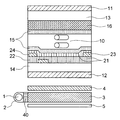
- a liquid crystal display panel of in-plan switching mode in which an electric field applied to a liquid crystal layer 10 is substantially parallel to a substrate is used as a normally-close type liquid crystal display utilizing birefringence of the first embodiment.
- the liquid crystal layer 10 is arranged between substrates 13 and 14 , and the substrates 13 and 14 are arranged between the polarizer plates 11 and 12 .
- An inner surface of the substrate 14 has stripe-shaped electrodes 22 and 23 , and a alignment layer 15 covering the electrodes 22 and 23 .
- the electrode 22 is a common electrode to which a voltage of predetermined wave form other than an image signal voltage is applied
- the electrode 23 is an image pixel electrode to which a wave form of voltage changeable in accordance with the image signal is applied.
- An image signal electrode 24 is arranged at the same height as the image pixel electrode 23 .
- An insulating layer 21 of silicon-nitride is formed between the electrodes.
- the substrate 13 has a color filter 16 for multi-color display. The color filter 16 may be formed on the substrate 14 with the electrodes.
- the alignment layer 15 is formed by coating the substrate with a solution of 3% concentration poly-amicacid, baking the poly-amicacid under 200° C., for 30 minutes to be changed to a polyimide layer, and rubbing a surface of the polyimide layer.
- the alignment layer 15 may be formed by being irradiated with a polarized ultraviolet rays.
- FIG. 2 shows a relationship in angle among the electric field 93 , a long axis 91 of liquid crystal molecule, and a polarized light transmitted axis 92 of the polarizer plate.
- the polarizing directions of the polarizer plates 11 and 12 are perpendicular to each other to form the normally-close type liquid crystal display utilizing birefringence.
- a luminous intensity of the transmitted light is calculated by the following formula wherein ⁇ n is an anisotropy in refractive index, ⁇ is an angle between the polarized light permeable axis and the long or effective axis 91 of liquid crystal molecule, d eff is a thickness of the liquid crystal layer, T 0 is a coefficient determined in accordance with a permeability of light of the polarizer plate, and ⁇ is a wave length of the light to be transmitted.
- T T 0 ⁇ sin 2 2 ⁇ sin 2 [( ⁇ d eff ⁇ n )/ ⁇ ]
- the liquid crystal layer 10 is a nematic liquid crystal of positive anisotropy in dielectric constant, the anisotropy in dielectric constant is 10.2, and the anisotropy in refractive index ⁇ n is 0.073.
- a permeability of light of the liquid crystal layer 10 is changed as shown in FIG. 3 .
- Areas (a) and (b) show a non-energized condition, and areas (b) and (d) show an energized condition in which the angle ⁇ between the long or effective axis 91 of liquid crystal molecule and the polarized light permeable axis 92 of the polarizer plate is changed by the electric field 93 .
- the inner surface of the substrate 14 has the stripe-shaped electrodes 22 and 23 , and the image signal electrodes 24 is arranged at the same height as the electrode 23 on the inner surface of the substrate 14 .
- a scanning electrode (gate wiring electrode) 25 extends perpendicularly to the image signal electrodes 24 .
- the alignment layer 15 is formed on the electrodes.
- An area on the substrate includes both an amorphous-silicon area 101 and a TFT element 102 .
- a liquid crystal display driver includes, for example, a common electrode driver circuit 103 , a vertical scanning signal circuit 104 , an image signal circuit 105 and an electric source and controller circuit 106 .
- FIG. 6 shows a spectrum generated by a cold cathode of narrow band light emitting type having a spectrum characteristic of a three band fluorescent light source.
- a peak in the spectrum is generated at a wave-length of 435 nm when this type fluorescent light source including mercury for energizing phosphor is used.
- the band-pass filter 40 is arranged between the cold cathode of narrow band light emitting type 1 and the light guide 3 .
- a plurality of sets each including a low refractive index dielectric layer such as magnesium-fluoride, silicon-oxide or the like, and a high refractive index dielectric layer such as zirconium-oxide, titanium-oxide or the like are stacked by a vapor deposition process until a number of layers reaches 6-20.
- the band-pass filter 40 absorbs effectively a light of wave-length not more than 440 nm, so that the blue fog phenomenon is restrained.
- a point A indicates to a chromaticity obtained by the prior art normally-close transverse electric field type liquid crystal display when a dark color is generated
- a point B indicates to a chromaticity obtained by the in-plane switching mode type liquid crystal display of the invention with the band-pass filter 40 when the dark color is generated
- a point A′ indicates to a chromaticity obtained by the prior art normally-close in-plane switching mode liquid crystal display when a bright color is generated
- a point B′ indicates to a chromaticity obtained by the in-plane switching mode liquid crystal display of the invention with the band-pass filter 40 when the bright color is generated.
- a point X indicates to a chromaticity of sun-light.
- An area of relatively small values of x and y corresponds to a relatively blue color
- an area of relatively large values of x and y corresponds to a relatively yellow color.
- the point A shows that the prior art normally-close transverse electric field type liquid crystal display emphasizes strongly the blue color
- the point B shows that the invention restrains the blue color from being emphasized.
- the points A′ and B′ show that the chromaticities by the transverse electric field type liquid crystal display of the invention and the prior art normally-close in-plane switching mode type liquid crystal display are not different largely from each other when the bright color is generated.
- the transverse electric field type liquid crystal display of the invention with the band-pass filter 40 restrains only the blue fog phenomenon, but does not have a large influence for the bright color indication.
- the band-pass filter 40 absorbs strongly the light of wave-length not more than 440 nm, but restrains the light of wave-length preferably more than 440 nm or practically not less than 450 nm from being absorbed strongly by the band-pass filter 40 .
- the light sources 1 are arranged at respective sides of a lower case 63 with an inverter drive circuit 64 .
- the reflecting plate 5 , the light guide 4 , the diffusion plate 4 and the liquid crystal display panel 70 are mounted on the lower case 63 .
- An upper side of the lower case 63 is covered by a shield case 61 having a display window.
- the light of wave-length not more than 440 nm does not have a large influence for brightness.
- a permeability of the light of wave-length 400-440 nm is high when a brightness of the normally-close in-plane switching mode liquid crystal display is low, and is low when a brightness of the normally-close in-plane switching mode liquid crystal display is high. Therefore, the blue fog phenomenon occurs and the brightness of display is not changed largely by the light of wave-length not more than 440 nm when brightness of the normally-close in-plane switching mode liquid crystal display is low, and the brightness of display is not changed largely by the light of wave-length not more than 440 nm when brightness of the normally-close in-plane switching mode liquid crystal display is high.
- a thick line 81 shows that a permeability of the light of wave-length not more than 440 nm is high and the permeability of the light decreases in accordance with an increase of the wave-length when the brightness is small
- a thin line 82 shows that a permeability of the light of wave-length not more than 440 nm is low and the permeability of the light increases in accordance with an increase of the wave-length when the brightness is high.
- a point Ha indicating a chromaticity obtained by the normally-close in-plane switching mode liquid crystal display including the band-pass filter 40 absorbing strongly the light of wave-length not more than 430 nm when the dark color is generated is not different largely from the point A indicating the chromaticity obtained by the prior art normally-close transverse electric field type liquid crystal display when the dark color is generated. Therefore, the normally-close transverse electric field type liquid crystal display including the band-pass filter 40 absorbing strongly the light of wave-length not more than 430 nm cannot restrain effectively the blue fog phenomenon.
- a point Hb indicating a chromaticity obtained by the normally-close transverse electric field type liquid crystal display including the band-pass filter 40 absorbing strongly the light of wave-length not more than 430 nm when the bright color is generated is not different largely from the point A′ indicating the chromaticity obtained by the prior art normally-close transverse electric field type liquid crystal display when the bright color is generated.
- a point Hc indicating a chromaticity obtained by the normally-close transverse electric field type liquid crystal display including the band-pass filter 40 absorbing strongly the light of wave-length not more than 450 nm when the dark color is generated is different largely from the point A indicating the chromaticity obtained by the prior art normally-close transverse electric field type liquid crystal display when the dark color is generated. Therefore, the normally-close transverse electric field type liquid crystal display including the band-pass filter 40 absorbing strongly the light of wave-length not more than 450 nm can restrain effectively the blue fog phenomenon.
- a point Hd indicating a chromaticity obtained by the normally-close transverse electric field type liquid crystal display including the band-pass filter 40 absorbing strongly the light of wave-length not more than 450 nm when the bright color is generated is different largely from the point A′ indicating the chromaticity obtained by the prior art normally-close transverse electric field type liquid crystal display when the bright color is generated. Therefore, yellow is emphasized in the bright color.
- a normally close STN type liquid crystal display has a transparent Y electrode on the transparent substrate 13 , a transparent X electrode on the transparent substrate 14 , the color filter 16 , a black matrix 17 and a flattening layer 18 .
- Each of the transparent substrates 13 and 14 between which the liquid crystal 10 is arranged has the directing layer 15 of polyimide whose surface is treated by rubbing.
- the X and Y electrodes are energized by a driver (not shown).
- the polarizer plate 11 and a phase plate 33 of polycarbonate are arranged at an outside of the transparent substrate 13
- the polarizer plate 12 and a phase plate 34 of polycarbonate are arranged at an outside of the transparent substrate 14 .
- the phase plate 34 may be arranged between the polarizer plate 11 and the phase plate 33 or between the substrate 13 and the phase plate 33 .
- the liquid crystal layer 10 of thickness 6.2 ⁇ m is a nematic liquid crystal of positive anisotropy in dielectric constant, and the anisotropy in refractive index ⁇ n is 0.144.
- the nematic liquid crystal includes a chiral agent (such as S 811 of Merc Inc.,) to have a twist angle of 240 degrees.
- an azimuth angle of the polarizing axis of the lower polarizer plate 12 is 10 degrees
- an azimuth angle of the polarizing axis of the upper polarizer plate 11 is 80 degrees
- an azimuth angle of slow axis of the lower phase plate 34 is 110 degrees
- an azimuth angle of slow axis of the upper phase plate 33 is 70 degrees
- retardations of the phase plates 33 and 34 are 400 nm.
- the azimuth angles are set in such a manner that the twist angle is 240 degrees, and rubbed angles of the upper and lower directing layers are ⁇ 30 degrees with respect to a longitudinal direction of the liquid crystal display panel.
- the arrangement of the light source unit and the band-pass filter 40 is the same as the embodiment shown in FIG. 1 .
- the band-pass filter 40 restrains the blue fog phenomenon in the normally close STN type liquid crystal display.
- a reflection and transmission combination STN type liquid crystal display panel has a transmission area formed by a transparent electrode 31 of, for example, ITO, and a reflection area formed by a reflection electrode 51 of, for example, aluminum in each pixel on the substrate 14 .
- a transparent electrode layer of, for example, ITO is deposited by sputtering process on the transparent substrate 14 , and a part of the transparent electrode layer is removed to form a pattern of the transparent electrode layer as the transparent electrode 31 .
- a reflection electrode layer of, for example, aluminum is deposited thereon, and a part of the reflection electrode layer is removed to form a pattern of the reflection electrode layer as the reflection electrode 52 .
- the color filter (not shown) is formed on the substrate.
- the reflection electrode may be formed on the transparent electrode.
- the transparent electrode and the reflection electrode may be driven electrically independently of each other.
- a band-pass filter 41 having the same absorption characteristic for the light as the band-pass filter 40 may be arranged between the light guide 3 and the diffusing plate 4 .
- the fluorescent light source 1 may be arranged under the light guide 3 .
- An acrylic type polymer layer including cyano-acrylate absorbent may be used as the band-pass filters 40 and 41 .
- the acrylic type polymer layer including cyano-acrylate absorbent may be formed on the light guide 3 by coating a rotated surface of the light guide 3 with the acrylic type polymer layer of monomer condition including cyano-acrylate absorbent, and polymerizing the acrylic type polymer layer of monomer condition including cyano-acrylate absorbent on the surface of the light guide 3 .
- the cyano-acrylate absorbent absorbs effectively the light of wave-length 400-440 nm.
- the acrylic type polymer layer including cyano-acrylate absorbent may be arranged directly on the three band fluorescent light source 1 or LED.
- the band-pass filters 40 or 41 may be arranged directly on the three band fluorescent light source 1 or LED.
- the light source may be formed by a combination of monochromatic red, green blue LEDs.
- the blue LED generates the light of wave-length 450-480 nm
- the green LED generates the light of wave-length 520-570 nm
- the red LED generates the light of wave-length 600-660 nm.
- An extremely small amount of light of wave-length not more than 440 nm is absorbed by the band-pass filters 40 and 41 between the light guide 3 and the diffusing plate 4 to restrain the blue fog phenomenon.
- the cyano-acrylate absorbent absorbing effectively the light of wave-length 400-440 nm may be included by the adhesive between the polarizer plate 12 and the phase plate 51 shown in FIG. 15 . In this case, the diffusing plate 4 is not necessary.
- the acrylic type polymer layer including cyano-acrylate absorbent absorbing effectively the light of wave-length 400-440 nm may be arranged on the substrate 13 .
- the band-pass filters 40 or 41 or the absorbent absorbing effectively the light of wave-length 400-440 nm may be arranged between the liquid crystal display panel and a viewer of the liquid crystal display.
- the color filter may includes the absorbent absorbing effectively the light of wave-length 400-440 nm.
- the absorbent absorbing effectively the light of wave-length may be included by a blue color filter or an overcoat layer of the color filter.
Abstract
Description
Claims (19)
Priority Applications (2)
| Application Number | Priority Date | Filing Date | Title |
|---|---|---|---|
| US10/692,931 US6850293B2 (en) | 2001-02-09 | 2003-10-27 | Liquid crystal display with absorber having absorption and permeability characteristics |
| US11/041,229 US7019799B2 (en) | 2001-02-09 | 2005-01-25 | Liquid crystal display with optical adjustment layer controlling transmittance of emitted light in accordance with wavelength |
Applications Claiming Priority (2)
| Application Number | Priority Date | Filing Date | Title |
|---|---|---|---|
| JP2001034014A JP3893533B2 (en) | 2001-02-09 | 2001-02-09 | Liquid crystal display |
| JP2001-034014 | 2001-02-09 |
Related Child Applications (1)
| Application Number | Title | Priority Date | Filing Date |
|---|---|---|---|
| US10/692,931 Continuation US6850293B2 (en) | 2001-02-09 | 2003-10-27 | Liquid crystal display with absorber having absorption and permeability characteristics |
Publications (2)
| Publication Number | Publication Date |
|---|---|
| US20020109809A1 US20020109809A1 (en) | 2002-08-15 |
| US6646699B2 true US6646699B2 (en) | 2003-11-11 |
Family
ID=18897689
Family Applications (3)
| Application Number | Title | Priority Date | Filing Date |
|---|---|---|---|
| US09/956,138 Expired - Lifetime US6646699B2 (en) | 2001-02-09 | 2001-09-20 | Liquid crystal display with band-pass filter |
| US10/692,931 Expired - Lifetime US6850293B2 (en) | 2001-02-09 | 2003-10-27 | Liquid crystal display with absorber having absorption and permeability characteristics |
| US11/041,229 Expired - Fee Related US7019799B2 (en) | 2001-02-09 | 2005-01-25 | Liquid crystal display with optical adjustment layer controlling transmittance of emitted light in accordance with wavelength |
Family Applications After (2)
| Application Number | Title | Priority Date | Filing Date |
|---|---|---|---|
| US10/692,931 Expired - Lifetime US6850293B2 (en) | 2001-02-09 | 2003-10-27 | Liquid crystal display with absorber having absorption and permeability characteristics |
| US11/041,229 Expired - Fee Related US7019799B2 (en) | 2001-02-09 | 2005-01-25 | Liquid crystal display with optical adjustment layer controlling transmittance of emitted light in accordance with wavelength |
Country Status (2)
| Country | Link |
|---|---|
| US (3) | US6646699B2 (en) |
| JP (1) | JP3893533B2 (en) |
Cited By (5)
| Publication number | Priority date | Publication date | Assignee | Title |
|---|---|---|---|---|
| US20030169385A1 (en) * | 2002-03-05 | 2003-09-11 | Citizen Electronics Co., Ltd. | Illumination device for a color liquid crystal display |
| US20050140855A1 (en) * | 2003-12-26 | 2005-06-30 | Yuka Utsumi | Liquid crystal display |
| US20050185112A1 (en) * | 2002-03-14 | 2005-08-25 | Nitto Denko Corporation | Back light and liquid crystal display unit using this |
| US20050206804A1 (en) * | 2002-03-14 | 2005-09-22 | Kazutaka Hara | Liquid crystal display unit |
| US20080284316A1 (en) * | 2007-05-18 | 2008-11-20 | Makoto Kurihara | Illuminating device, display device and optical film |
Families Citing this family (15)
| Publication number | Priority date | Publication date | Assignee | Title |
|---|---|---|---|---|
| US7030945B2 (en) * | 2001-08-22 | 2006-04-18 | Nitto Denko Corporation | Liquid-crystal display device |
| JP4757545B2 (en) * | 2004-06-21 | 2011-08-24 | 株式会社 日立ディスプレイズ | Liquid crystal display |
| JP4527512B2 (en) * | 2004-12-08 | 2010-08-18 | Nec液晶テクノロジー株式会社 | Liquid crystal display |
| JP2007147884A (en) * | 2005-11-25 | 2007-06-14 | Nitto Denko Corp | Liquid crystal display device |
| JP5095993B2 (en) * | 2006-12-28 | 2012-12-12 | 株式会社ジャパンディスプレイイースト | Liquid crystal display, plasma display |
| JP2010243894A (en) * | 2009-04-08 | 2010-10-28 | Hitachi Displays Ltd | Liquid crystal display device |
| JP2013089559A (en) * | 2011-10-21 | 2013-05-13 | Minebea Co Ltd | Planar lighting device |
| US10901125B2 (en) | 2014-05-23 | 2021-01-26 | Eyesafe, Llc | Light emission reducing compounds for electronic devices |
| US10642087B2 (en) | 2014-05-23 | 2020-05-05 | Eyesafe, Llc | Light emission reducing compounds for electronic devices |
| US10330850B2 (en) * | 2016-09-26 | 2019-06-25 | Samsung Display Co., Ltd. | Display apparatus |
| US10955697B2 (en) | 2018-11-28 | 2021-03-23 | Eyesafe Inc. | Light emission modification |
| US11592701B2 (en) | 2018-11-28 | 2023-02-28 | Eyesafe Inc. | Backlight unit with emission modification |
| US11126033B2 (en) | 2018-11-28 | 2021-09-21 | Eyesafe Inc. | Backlight unit with emission modification |
| US11810532B2 (en) | 2018-11-28 | 2023-11-07 | Eyesafe Inc. | Systems for monitoring and regulating harmful blue light exposure from digital devices |
| US10971660B2 (en) | 2019-08-09 | 2021-04-06 | Eyesafe Inc. | White LED light source and method of making same |
Citations (7)
| Publication number | Priority date | Publication date | Assignee | Title |
|---|---|---|---|---|
| JPH03296720A (en) * | 1990-04-17 | 1991-12-27 | Citizen Watch Co Ltd | Optical modulating device |
| US5754262A (en) * | 1995-04-11 | 1998-05-19 | Litton Systems, Inc. | Daylight readable liquid crystal display |
| US20010002146A1 (en) * | 1997-07-12 | 2001-05-31 | Lg Electronics Inc. | In-plane switching mode liquid crystal display device |
| US6297907B1 (en) * | 1997-09-02 | 2001-10-02 | California Institute Of Technology | Devices based on surface plasmon interference filters |
| US20010038425A1 (en) * | 1998-08-04 | 2001-11-08 | James Y. Lee | Backlight assembly for a display device |
| US20010052955A1 (en) * | 2000-06-08 | 2001-12-20 | Fujitsu Limited | Backlight unit and liquid crystal device using backlight units |
| US6437840B1 (en) * | 1997-06-09 | 2002-08-20 | Seiko Epson Corporation | Display device having a light emitting element |
Family Cites Families (27)
| Publication number | Priority date | Publication date | Assignee | Title |
|---|---|---|---|---|
| JPH0262515A (en) * | 1988-08-29 | 1990-03-02 | Matsushita Electric Ind Co Ltd | Liquid crystal display device |
| JPH0642125B2 (en) * | 1988-10-04 | 1994-06-01 | シャープ株式会社 | Projection equipment |
| JPH03206720A (en) | 1990-01-08 | 1991-09-10 | Nec Corp | Dynamic frequency divider |
| JP3102012B2 (en) * | 1990-03-30 | 2000-10-23 | 科学技術振興事業団 | Tunable optical bandpass filter |
| JPH06308473A (en) * | 1993-04-20 | 1994-11-04 | Sumitomo Electric Ind Ltd | Transparent conductive base material and liquid crystal element using the same |
| JP3274244B2 (en) * | 1993-09-06 | 2002-04-15 | 株式会社東芝 | Liquid crystal display |
| JP3000560U (en) * | 1994-01-31 | 1994-08-09 | 株式会社島津製作所 | Color liquid crystal display |
| JPH07318929A (en) * | 1994-05-30 | 1995-12-08 | Casio Comput Co Ltd | Liquid crystal display device |
| JPH0815697A (en) | 1994-06-29 | 1996-01-19 | Hitachi Ltd | Liquid crystal display device |
| JPH0862568A (en) * | 1994-08-19 | 1996-03-08 | Hitachi Ltd | Liquid crystal display device |
| JPH0973083A (en) * | 1995-09-05 | 1997-03-18 | Toshiba Corp | Illuminator and liquid crystal display device |
| JP2740135B2 (en) * | 1995-02-17 | 1998-04-15 | 大成化工株式会社 | Simple absorbance meter |
| US6018421A (en) * | 1995-06-28 | 2000-01-25 | Cushing; David Henry | Multilayer thin film bandpass filter |
| JP3458562B2 (en) * | 1995-10-12 | 2003-10-20 | 株式会社日立製作所 | Liquid crystal display device and manufacturing method thereof |
| JP3740788B2 (en) | 1996-05-08 | 2006-02-01 | 株式会社日立製作所 | Active matrix liquid crystal display device |
| US5834122A (en) * | 1996-11-25 | 1998-11-10 | Hoechst Celanese Corp. | Spectrally tuned multiple bandpass filters for video displays |
| JP3460588B2 (en) * | 1997-09-18 | 2003-10-27 | セイコーエプソン株式会社 | Display device and electronic device using the same |
| JP4149021B2 (en) * | 1998-01-14 | 2008-09-10 | オリンパス株式会社 | Optical system |
| JPH11231301A (en) * | 1998-02-10 | 1999-08-27 | Kureha Chem Ind Co Ltd | Color image display device |
| JPH11258597A (en) * | 1998-03-11 | 1999-09-24 | Alps Electric Co Ltd | Reflection type liquid crystal display device |
| JPH11306836A (en) * | 1998-04-17 | 1999-11-05 | Ichikoh Ind Ltd | Flat surface color light emission device |
| JP2000019543A (en) | 1998-04-27 | 2000-01-21 | Hitachi Ltd | Active matrix type liquid crystal display device |
| EP1482332B1 (en) * | 1998-05-15 | 2010-11-03 | Toyo Boseki Kabushiki Kaisha | Infrared absorption filter |
| JP3419317B2 (en) * | 1998-08-21 | 2003-06-23 | セイコーエプソン株式会社 | Liquid crystal display device and electronic device using the same |
| JP2000156108A (en) * | 1998-11-20 | 2000-06-06 | Toshiba Corp | Planar display device |
| JP2000206544A (en) | 1999-01-08 | 2000-07-28 | Hitachi Ltd | Liquid crystal display device |
| JP2001242315A (en) * | 2000-02-29 | 2001-09-07 | Fuji Photo Film Co Ltd | Cholesteric liquid crystal color filter, its manufacturing method and display device utilizing the same |
-
2001
- 2001-02-09 JP JP2001034014A patent/JP3893533B2/en not_active Expired - Fee Related
- 2001-09-20 US US09/956,138 patent/US6646699B2/en not_active Expired - Lifetime
-
2003
- 2003-10-27 US US10/692,931 patent/US6850293B2/en not_active Expired - Lifetime
-
2005
- 2005-01-25 US US11/041,229 patent/US7019799B2/en not_active Expired - Fee Related
Patent Citations (7)
| Publication number | Priority date | Publication date | Assignee | Title |
|---|---|---|---|---|
| JPH03296720A (en) * | 1990-04-17 | 1991-12-27 | Citizen Watch Co Ltd | Optical modulating device |
| US5754262A (en) * | 1995-04-11 | 1998-05-19 | Litton Systems, Inc. | Daylight readable liquid crystal display |
| US6437840B1 (en) * | 1997-06-09 | 2002-08-20 | Seiko Epson Corporation | Display device having a light emitting element |
| US20010002146A1 (en) * | 1997-07-12 | 2001-05-31 | Lg Electronics Inc. | In-plane switching mode liquid crystal display device |
| US6297907B1 (en) * | 1997-09-02 | 2001-10-02 | California Institute Of Technology | Devices based on surface plasmon interference filters |
| US20010038425A1 (en) * | 1998-08-04 | 2001-11-08 | James Y. Lee | Backlight assembly for a display device |
| US20010052955A1 (en) * | 2000-06-08 | 2001-12-20 | Fujitsu Limited | Backlight unit and liquid crystal device using backlight units |
Cited By (9)
| Publication number | Priority date | Publication date | Assignee | Title |
|---|---|---|---|---|
| US20030169385A1 (en) * | 2002-03-05 | 2003-09-11 | Citizen Electronics Co., Ltd. | Illumination device for a color liquid crystal display |
| US20050185112A1 (en) * | 2002-03-14 | 2005-08-25 | Nitto Denko Corporation | Back light and liquid crystal display unit using this |
| US20050206804A1 (en) * | 2002-03-14 | 2005-09-22 | Kazutaka Hara | Liquid crystal display unit |
| US20050140855A1 (en) * | 2003-12-26 | 2005-06-30 | Yuka Utsumi | Liquid crystal display |
| US7489374B2 (en) * | 2003-12-26 | 2009-02-10 | Hitachi Displays, Ltd. | Liquid crystal display |
| US20090141220A1 (en) * | 2003-12-26 | 2009-06-04 | Yuka Utsumi | Liquid Crystal Display |
| US8059235B2 (en) * | 2003-12-26 | 2011-11-15 | Hitachi Displays, Ltd. | Liquid crystal display |
| US20080284316A1 (en) * | 2007-05-18 | 2008-11-20 | Makoto Kurihara | Illuminating device, display device and optical film |
| US7859175B2 (en) * | 2007-05-18 | 2010-12-28 | Seiko Instruments Inc. | Illuminating device, display device and optical film |
Also Published As
| Publication number | Publication date |
|---|---|
| US6850293B2 (en) | 2005-02-01 |
| US20050128378A1 (en) | 2005-06-16 |
| US7019799B2 (en) | 2006-03-28 |
| US20040085494A1 (en) | 2004-05-06 |
| JP3893533B2 (en) | 2007-03-14 |
| JP2002236289A (en) | 2002-08-23 |
| US20020109809A1 (en) | 2002-08-15 |
Similar Documents
| Publication | Publication Date | Title |
|---|---|---|
| US7019799B2 (en) | Liquid crystal display with optical adjustment layer controlling transmittance of emitted light in accordance with wavelength | |
| JP3380482B2 (en) | Liquid crystal display | |
| US20100165278A1 (en) | Liquid crystal display device | |
| US6970215B2 (en) | Reflective LCD, semitransmitting reflective LCD and electronic device | |
| KR20030017379A (en) | Liquid crystal display | |
| JP2003215342A (en) | Light reflector, method for producing the same, liquid crystal device and electronic device | |
| JP2010266610A (en) | Liquid crystal display | |
| JP3310569B2 (en) | Reflective liquid crystal display | |
| JP2000066195A (en) | Reflection type liquid crystal display device | |
| US6693688B1 (en) | Flat display device | |
| JPH1164837A (en) | Liquid crystal display device | |
| JP3256656B2 (en) | Deflection element | |
| JP3654317B2 (en) | Color LCD panel | |
| JPH1138397A (en) | Reflection type color liquid crystal display element | |
| JP2006301634A (en) | Display panel, method of manufacturing the same and display device having the same | |
| EP1116986A1 (en) | Reflection liquid crystal display | |
| JPH07239471A (en) | Reflection type liquid crystal display device | |
| JP2002372710A (en) | Liquid crystal display device | |
| JP3464475B2 (en) | Liquid crystal display | |
| JP2002182191A (en) | Electrooptic device and electronic equipment | |
| US20230129697A1 (en) | Liquid crystal panel and display device | |
| JP7391686B2 (en) | Method for manufacturing a liquid crystal display device and liquid crystal display device | |
| JP2002333624A (en) | Liquid crystal display device | |
| KR20000042075A (en) | Display device | |
| JP2000029021A (en) | Reflective liquid crystal display device |
Legal Events
| Date | Code | Title | Description |
|---|---|---|---|
| AS | Assignment |
Owner name: HITACHI, LTD., JAPAN Free format text: ASSIGNMENT OF ASSIGNORS INTEREST;ASSIGNORS:UTSUMI, YUKA;HIYAMA, IKUO;KOMURA, SHINICHI;AND OTHERS;REEL/FRAME:012310/0640;SIGNING DATES FROM 20010905 TO 20010912 |
|
| STCF | Information on status: patent grant |
Free format text: PATENTED CASE |
|
| FEPP | Fee payment procedure |
Free format text: PAYOR NUMBER ASSIGNED (ORIGINAL EVENT CODE: ASPN); ENTITY STATUS OF PATENT OWNER: LARGE ENTITY |
|
| FPAY | Fee payment |
Year of fee payment: 4 |
|
| FPAY | Fee payment |
Year of fee payment: 8 |
|
| AS | Assignment |
Owner name: PANASONIC LIQUID CRYSTAL DISPLAY CO., LTD., JAPAN Free format text: MERGER/CHANGE OF NAME;ASSIGNOR:IPS ALPHA SUPPORT CO., LTD.;REEL/FRAME:027363/0315 Effective date: 20101001 Owner name: IPS ALPHA SUPPORT CO., LTD., JAPAN Free format text: COMPANY SPLIT PLAN TRANSFERRING FIFTY (50) PERCENT SHARE OF PATENTS AND PATENT APPLICATIONS;ASSIGNOR:HITACHI DISPLAYS, LTD.;REEL/FRAME:027362/0466 Effective date: 20100630 Owner name: HITACHI DISPLAYS, LTD., JAPAN Free format text: COMPANY SPLIT PLAN TRANSFERRING ONE HUNDRED (100) PERCENT SHARE OF PATENT AND PATENT APPLICATIONS;ASSIGNOR:HITACHI, LTD.;REEL/FRAME:027362/0612 Effective date: 20021001 |
|
| FPAY | Fee payment |
Year of fee payment: 12 |