US6665026B2 - Liquid crystal display - Google Patents
Liquid crystal display Download PDFInfo
- Publication number
- US6665026B2 US6665026B2 US09/865,435 US86543501A US6665026B2 US 6665026 B2 US6665026 B2 US 6665026B2 US 86543501 A US86543501 A US 86543501A US 6665026 B2 US6665026 B2 US 6665026B2
- Authority
- US
- United States
- Prior art keywords
- liquid crystal
- crystal display
- layer
- substrate
- polarizer
- Prior art date
- Legal status (The legal status is an assumption and is not a legal conclusion. Google has not performed a legal analysis and makes no representation as to the accuracy of the status listed.)
- Expired - Fee Related, expires
Links
Images


Classifications
-
- G—PHYSICS
- G02—OPTICS
- G02F—OPTICAL DEVICES OR ARRANGEMENTS FOR THE CONTROL OF LIGHT BY MODIFICATION OF THE OPTICAL PROPERTIES OF THE MEDIA OF THE ELEMENTS INVOLVED THEREIN; NON-LINEAR OPTICS; FREQUENCY-CHANGING OF LIGHT; OPTICAL LOGIC ELEMENTS; OPTICAL ANALOGUE/DIGITAL CONVERTERS
- G02F1/00—Devices or arrangements for the control of the intensity, colour, phase, polarisation or direction of light arriving from an independent light source, e.g. switching, gating or modulating; Non-linear optics
- G02F1/01—Devices or arrangements for the control of the intensity, colour, phase, polarisation or direction of light arriving from an independent light source, e.g. switching, gating or modulating; Non-linear optics for the control of the intensity, phase, polarisation or colour
- G02F1/13—Devices or arrangements for the control of the intensity, colour, phase, polarisation or direction of light arriving from an independent light source, e.g. switching, gating or modulating; Non-linear optics for the control of the intensity, phase, polarisation or colour based on liquid crystals, e.g. single liquid crystal display cells
- G02F1/133—Constructional arrangements; Operation of liquid crystal cells; Circuit arrangements
- G02F1/1333—Constructional arrangements; Manufacturing methods
- G02F1/1347—Arrangement of liquid crystal layers or cells in which the final condition of one light beam is achieved by the addition of the effects of two or more layers or cells
- G02F1/13471—Arrangement of liquid crystal layers or cells in which the final condition of one light beam is achieved by the addition of the effects of two or more layers or cells in which all the liquid crystal cells or layers remain transparent, e.g. FLC, ECB, DAP, HAN, TN, STN, SBE-LC cells
Definitions
- the present invention relates to a liquid crystal display that is composed of at least two stacked liquid crystal display units.
- Liquid crystal display has been used in many fields, e.g., electric shutters for cameras. Electric shutters are designed to fulfill the need of formation of three-dimensional image that cannot be achieved by mechanic shutters. Nevertheless, the screening range of the conventional liquid crystal display for electric shutters is poor. More specifically, the screening range of the conventional liquid crystal display for electric shutters is about 0 ⁇ 5 degrees, as shown in FIG. 6 . Residual image is thus generated. As a result, the resultant image is not clear as having an overlapped portion. In addition, the conventional liquid crystal display has limits in view orientation, view angle, and contrast.
- the user of a camera having an electric shutter using conventional liquid crystal cannot obtain clear image unless the camera is used in special view orientations, at special view angles, and has special color contrast Furthermore, the right eye sees a portion of the image in the left eye and the left eye sees a portion of the image in the right eye. Namely, the two images in the right and left eyes have an overlapped portion. This causes pressure to the brain and the vision system and the user has eyestrain. It takes a period of time for the user to recover after he/she has get used to the overlapping of images. This problem aggravates when the user is an aged person or a child.
- the present invention is intended to provide an improved liquid crystal display that mitigates and/or obviates the above problems.
- a liquid crystal display in accordance with the present invention comprises at least two liquid crystal display units that are stacked up one another.
- Each liquid crystal display unit comprises, from top to bottom, a first polarizer, a first substrate, a first pile layer, a liquid crystal layer, a second pile layer, a second substrate, and a second polarizer.
- the first and second substrates are made from glass.
- the liquid crystal layer has a twist angle of zero or greater than zero. All of the first polarizer, the first substrate, the first pile layer, the liquid crystal layer, the second pile layer, the second substrate, and the second polarizer in each said liquid crystal display unit are adhered to each other by means of whole-face bonding by transparent or non-transparent glue. Alternatively, all of the first polarizer, the first substrate, the first pile layer, the liquid crystal layer, the second pile layer, the second substrate, and the second polarizer in each said liquid crystal display unit are adhered to each other by means of peripheral-bonding by transparent or non-transparent glue.
- the first glass substrate and the first pile layer have a conductive layer therebetween.
- the first glass substrate and the first pile layer have a conductive layer and an insulating layer therebetween.
- the second glass substrate and the second pile layer have a conductive layer therebetween.
- the second glass substrate and the second pile layer have a conductive layer and an insulating layer therebetween.
- Each of the first substrate and the second substrate has a seal applied to a periphery thereof, thereby providing a sealed space for receiving liquid crystal that forms the liquid crystal layer.
- One of the second polarizer of an upper one of two stacked said liquid crystal display units and the first polarizer of a lower one of the two stacked said liquid crystal units may be removed such that two adjacent stacked liquid crystal display units share a common polarizer therebetween.
- FIG. 1 is a sectional view of a liquid crystal display in accordance with the present invention.
- FIG. 2 is a sectional view of a modified embodiment of the liquid crystal display in accordance with the present invention.
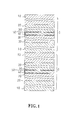
- FIG. 3 is a perspective view of the modified embodiment of the liquid crystal display in FIG. 2 .
- FIG. 4 is a sectional view of another modified embodiment of the liquid crystal display in accordance with the present invention.
- FIG. 5 is a schematic diagram illustrating the screening range of the liquid crystal display in accordance with the present invention.
- FIG. 6 is a schematic diagram illustrating the screening range of a conventional liquid crystal display.
- FIG. 1 shows two liquid crystal display units 1 that are stacked up one upon the other to form the liquid crystal display in accordance with the present invention having a better screening effect.
- Each liquid crystal unit 1 includes, from top to bottom, a first polarizer 10 , a first glass substrate 20 , a first pile layer 30 , a liquid crystal layer 40 , a second pile layer 30 , a second glass substrate 20 , and a second polarizer 10 .
- Seal 50 is applied to a periphery of each glass substrate 20 , thereby providing a sealed space between the first glass substrate 20 and the second glass substrate 20 for receiving the liquid crystal that forms the liquid crystal layer 40 .
- Each polarizer 10 allows relative light waves to pass therethrough.
- Each glass substrate 20 is transparent to allow image light waves to pass therethrough.
- Each pile layer 30 can be disposed according to need, so as to match different view angles.
- the liquid crystal layer 40 has a twist angle of zero or greater than zero.
- the two liquid crystal display units 1 are stacked up one upon the other to form the liquid crystal display in accordance with the present invention having a better screening effect.
- the number of the liquid crystal display units 1 is not limited. Namely, one may stack up the liquid crystal display units 1 as many as he/she wishes.
- the layers in each liquid crystal display unit 1 are adhered to each other by means of whole-face bonding by transparent or non-transparent glue, such as thermosetting glue, AB(two component liquid adhesive) glue, or UV(ultra light-weld adhesive) glue.
- each liquid crystal display unit is adhered to each other by means of peripheral bonding by transparent or non-transparent double-sided tape, epoxy resin, thermosetting glue, AB(two component liquid adhesive) glue, or UV(ultra light-weld adhesive) glue.
- the liquid crystal layer 40 may be colored to increase the screening effect.
- the effective screening range of the resultant liquid crystal display in accordance with the present invention is broadened to be about 0 ⁇ 35 degrees.
- the liquid crystal display in accordance with the present invention may be operated in wider view orientations and view angles and provide a better contrast effect.
- the liquid crystal display in accordance with the present invention may be used in electric shutters that require higher screening effect.
- the dead angle for screening is obviated by the liquid crystal display formed by at least two stacked liquid crystal display units.
- the view angle for forming image becomes larger and the resultant three-dimensional image is very clear.
- the liquid crystal display thus formed causes less harm to the vision system of the user even after a long-term use.
- the image in the right eye of the user and the image of the left eye of the user are not overlapped, thereby forming a three-dimensional image in the brain.
- FIGS. 2 and 3 show a modified embodiment of the invention, wherein one of the second polarizer 10 of an upper one of two stacked liquid crystal display units 1 and the first polarizer 10 of a lower one of the two stacked liquid crystal units 1 is removed.
- FIG. 4 illustrates another modified embodiment of the invention, wherein a conductive layer 60 and an optional insulating layer 70 is provided between the glass substrate 20 and the pile layer 30 .
- the liquid crystal display in accordance with the present invention can be used in many fields, not limited to electric shutters.
Abstract
Description
Claims (13)
Applications Claiming Priority (2)
| Application Number | Priority Date | Filing Date | Title |
|---|---|---|---|
| TW089208459U TWM272104U (en) | 2000-05-19 | 2000-05-19 | Liquid crystal shutter display |
| TW089208459 | 2000-05-19 |
Publications (2)
| Publication Number | Publication Date |
|---|---|
| US20010043295A1 US20010043295A1 (en) | 2001-11-22 |
| US6665026B2 true US6665026B2 (en) | 2003-12-16 |
Family
ID=21668065
Family Applications (1)
| Application Number | Title | Priority Date | Filing Date |
|---|---|---|---|
| US09/865,435 Expired - Fee Related US6665026B2 (en) | 2000-05-19 | 2001-05-29 | Liquid crystal display |
Country Status (2)
| Country | Link |
|---|---|
| US (1) | US6665026B2 (en) |
| TW (1) | TWM272104U (en) |
Cited By (1)
| Publication number | Priority date | Publication date | Assignee | Title |
|---|---|---|---|---|
| US20070115211A1 (en) * | 2005-11-23 | 2007-05-24 | Hon Hai Precision Industry Co., Ltd. | Liquid crystal shutter device for a camera |
Families Citing this family (7)
| Publication number | Priority date | Publication date | Assignee | Title |
|---|---|---|---|---|
| DE10327946A1 (en) * | 2003-06-20 | 2005-01-20 | United Radiant Technology, Corp. | Liquid crystal shutter e.g. for camera, comprises two or more LC units stacked together and joined e.g. by transparent adhesive. |
| US7773064B2 (en) * | 2003-07-02 | 2010-08-10 | Kent Displays Incorporated | Liquid crystal display films |
| CN1914031B (en) | 2004-01-28 | 2011-11-16 | 肯特显示器公司 | Drapable liquid crystal transfer display films |
| US8451201B2 (en) * | 2005-09-30 | 2013-05-28 | Sharp Kabushiki Kaisha | Liquid crystal display device drive method, liquid crystal display device, and television receiver |
| CN101523477A (en) * | 2006-11-20 | 2009-09-02 | 夏普株式会社 | Display apparatus driving method, driver circuit, liquid crystal display apparatus, and television receiver |
| CN104390177A (en) * | 2014-11-14 | 2015-03-04 | 深圳市华星光电技术有限公司 | Backlight module |
| US11567375B2 (en) * | 2021-01-29 | 2023-01-31 | Meta Platforms, Inc. | Techniques for complex wavefront modulation |
Citations (7)
| Publication number | Priority date | Publication date | Assignee | Title |
|---|---|---|---|---|
| US4842379A (en) * | 1986-11-13 | 1989-06-27 | Fuji Photo Film Co., Ltd. | Image recording apparatus utilizing an ECB mode liquid crystal |
| US4966441A (en) * | 1989-03-28 | 1990-10-30 | In Focus Systems, Inc. | Hybrid color display system |
| US5122887A (en) * | 1991-03-05 | 1992-06-16 | Sayett Group, Inc. | Color display utilizing twisted nematic LCDs and selective polarizers |
| US5726723A (en) * | 1996-01-31 | 1998-03-10 | Technology Research International Corporation | Sub-twisted nematic liquid crystal display |
| US5751385A (en) * | 1994-06-07 | 1998-05-12 | Honeywell, Inc. | Subtractive color LCD utilizing circular notch polarizers and including a triband or broadband filter tuned light source or dichroic sheet color polarizers |
| US6437843B1 (en) * | 1999-04-08 | 2002-08-20 | Koninklijke Philips Electronics N.V. | Double cell liquid crystal |
| US6504588B1 (en) * | 1998-04-28 | 2003-01-07 | Citizen Watch Co., Ltd. | Reflection-type color liquid crystal display device having absorbing member containing fluorescent material |
-
2000
- 2000-05-19 TW TW089208459U patent/TWM272104U/en unknown
-
2001
- 2001-05-29 US US09/865,435 patent/US6665026B2/en not_active Expired - Fee Related
Patent Citations (7)
| Publication number | Priority date | Publication date | Assignee | Title |
|---|---|---|---|---|
| US4842379A (en) * | 1986-11-13 | 1989-06-27 | Fuji Photo Film Co., Ltd. | Image recording apparatus utilizing an ECB mode liquid crystal |
| US4966441A (en) * | 1989-03-28 | 1990-10-30 | In Focus Systems, Inc. | Hybrid color display system |
| US5122887A (en) * | 1991-03-05 | 1992-06-16 | Sayett Group, Inc. | Color display utilizing twisted nematic LCDs and selective polarizers |
| US5751385A (en) * | 1994-06-07 | 1998-05-12 | Honeywell, Inc. | Subtractive color LCD utilizing circular notch polarizers and including a triband or broadband filter tuned light source or dichroic sheet color polarizers |
| US5726723A (en) * | 1996-01-31 | 1998-03-10 | Technology Research International Corporation | Sub-twisted nematic liquid crystal display |
| US6504588B1 (en) * | 1998-04-28 | 2003-01-07 | Citizen Watch Co., Ltd. | Reflection-type color liquid crystal display device having absorbing member containing fluorescent material |
| US6437843B1 (en) * | 1999-04-08 | 2002-08-20 | Koninklijke Philips Electronics N.V. | Double cell liquid crystal |
Cited By (2)
| Publication number | Priority date | Publication date | Assignee | Title |
|---|---|---|---|---|
| US20070115211A1 (en) * | 2005-11-23 | 2007-05-24 | Hon Hai Precision Industry Co., Ltd. | Liquid crystal shutter device for a camera |
| US7450187B2 (en) * | 2005-11-23 | 2008-11-11 | Hon Hai Precision Industry Co., Ltd. | Liquid crystal shutter device for a camera |
Also Published As
| Publication number | Publication date |
|---|---|
| US20010043295A1 (en) | 2001-11-22 |
| TWM272104U (en) | 2005-08-01 |
Similar Documents
| Publication | Publication Date | Title |
|---|---|---|
| JP4607089B2 (en) | Liquid crystal lens and video display device including the same | |
| KR101530619B1 (en) | 3D display panel and method of manufacturing phase difference plate | |
| CN102870033B (en) | Bendable liquid crystal polarization switch for direct view stereoscopic display | |
| TW200410565A (en) | Liquid crystal display panel and liquid crystal display device | |
| WO2016090974A1 (en) | Multi-sided display device | |
| WO2017117988A1 (en) | Backlight module, display device and driving method therefor | |
| US6665026B2 (en) | Liquid crystal display | |
| WO2020113428A1 (en) | Display panel, display device and display method | |
| WO2016090871A1 (en) | Multi-sided display device | |
| US20170351105A1 (en) | Thin film with integrated grating and polarizer, manufacturing method thereof, and display device | |
| TWI684811B (en) | Display device and method of manufacturing display device | |
| CN112835207A (en) | Display module and electronic equipment | |
| CN1664660B (en) | Reflection type liquid crystal display device, display apparatus and projection system | |
| WO2020215707A1 (en) | Display panel and electronic device | |
| KR20230093207A (en) | Foldable display device | |
| CN106483670B (en) | Polarization control panel and its manufacturing method and the 3 d display device for using it | |
| US20170153494A1 (en) | Multi-curved liquid crystal display panel | |
| TW201226982A (en) | Image display device | |
| JPH04207774A (en) | Liquid crystal projection type television and liquid crystal projection type color television using same | |
| US9784981B2 (en) | Liquid crystal display device and liquid crystal display module thereof | |
| JPH08171098A (en) | Liquid crystal shutter and stereoscopic image recognizing spectacles | |
| JPS6111788A (en) | Image display | |
| CN205861932U (en) | A kind of 3D glasses light polarizing film of plastic type | |
| JP2003005195A (en) | Liquid crystal display device | |
| US20030025862A1 (en) | Liquid crystal projector |
Legal Events
| Date | Code | Title | Description |
|---|---|---|---|
| AS | Assignment |
Owner name: LIN, SUNG-PEN, TAIWAN Free format text: ASSIGNMENT OF ASSIGNORS INTEREST;ASSIGNORS:WANG, PEI-CHANG;CHEN, MENG-TE;REEL/FRAME:011852/0001 Effective date: 20010522 |
|
| AS | Assignment |
Owner name: UNITED RADIANT TECHNOLOGY CORP., TAIWAN Free format text: ASSIGNMENT OF ASSIGNORS INTEREST;ASSIGNOR:LIN, SUNG-PEN;REEL/FRAME:018061/0605 Effective date: 20060803 |
|
| FEPP | Fee payment procedure |
Free format text: PAT HOLDER CLAIMS SMALL ENTITY STATUS, ENTITY STATUS SET TO SMALL (ORIGINAL EVENT CODE: LTOS); ENTITY STATUS OF PATENT OWNER: SMALL ENTITY Free format text: PAYOR NUMBER ASSIGNED (ORIGINAL EVENT CODE: ASPN); ENTITY STATUS OF PATENT OWNER: SMALL ENTITY |
|
| FPAY | Fee payment |
Year of fee payment: 4 |
|
| FPAY | Fee payment |
Year of fee payment: 8 |
|
| REMI | Maintenance fee reminder mailed | ||
| LAPS | Lapse for failure to pay maintenance fees | ||
| STCH | Information on status: patent discontinuation |
Free format text: PATENT EXPIRED DUE TO NONPAYMENT OF MAINTENANCE FEES UNDER 37 CFR 1.362 |
|
| FP | Lapsed due to failure to pay maintenance fee |
Effective date: 20151216 |