US6674124B2 - Trench MOSFET having low gate charge - Google Patents
Trench MOSFET having low gate charge Download PDFInfo
- Publication number
- US6674124B2 US6674124B2 US10/002,529 US252901A US6674124B2 US 6674124 B2 US6674124 B2 US 6674124B2 US 252901 A US252901 A US 252901A US 6674124 B2 US6674124 B2 US 6674124B2
- Authority
- US
- United States
- Prior art keywords
- trench
- region
- oxide
- epitaxial layer
- mosfet device
- Prior art date
- Legal status (The legal status is an assumption and is not a legal conclusion. Google has not performed a legal analysis and makes no representation as to the accuracy of the status listed.)
- Expired - Lifetime
Links
- 239000000758 substrate Substances 0.000 claims abstract description 33
- 210000000746 body region Anatomy 0.000 claims abstract description 26
- XUIMIQQOPSSXEZ-UHFFFAOYSA-N Silicon Chemical compound [Si] XUIMIQQOPSSXEZ-UHFFFAOYSA-N 0.000 claims abstract description 25
- 229910052710 silicon Inorganic materials 0.000 claims abstract description 25
- 239000010703 silicon Substances 0.000 claims abstract description 25
- 229910021420 polycrystalline silicon Inorganic materials 0.000 claims description 48
- 239000003870 refractory metal Substances 0.000 claims description 12
- BOTDANWDWHJENH-UHFFFAOYSA-N Tetraethyl orthosilicate Chemical compound CCO[Si](OCC)(OCC)OCC BOTDANWDWHJENH-UHFFFAOYSA-N 0.000 claims description 10
- 229910021341 titanium silicide Inorganic materials 0.000 claims description 7
- WFKWXMTUELFFGS-UHFFFAOYSA-N tungsten Chemical compound [W] WFKWXMTUELFFGS-UHFFFAOYSA-N 0.000 claims description 7
- 229910052721 tungsten Inorganic materials 0.000 claims description 7
- 239000010937 tungsten Substances 0.000 claims description 7
- 229910001080 W alloy Inorganic materials 0.000 claims description 5
- 229910021332 silicide Inorganic materials 0.000 claims description 5
- MAKDTFFYCIMFQP-UHFFFAOYSA-N titanium tungsten Chemical compound [Ti].[W] MAKDTFFYCIMFQP-UHFFFAOYSA-N 0.000 claims description 5
- FVBUAEGBCNSCDD-UHFFFAOYSA-N silicide(4-) Chemical compound [Si-4] FVBUAEGBCNSCDD-UHFFFAOYSA-N 0.000 claims description 4
- 229910001092 metal group alloy Inorganic materials 0.000 claims description 3
- 229920005591 polysilicon Polymers 0.000 description 39
- 238000000034 method Methods 0.000 description 25
- 229910052751 metal Inorganic materials 0.000 description 14
- 239000002184 metal Substances 0.000 description 14
- 230000003647 oxidation Effects 0.000 description 13
- 238000007254 oxidation reaction Methods 0.000 description 13
- 229920002120 photoresistant polymer Polymers 0.000 description 11
- VYPSYNLAJGMNEJ-UHFFFAOYSA-N Silicium dioxide Chemical group O=[Si]=O VYPSYNLAJGMNEJ-UHFFFAOYSA-N 0.000 description 10
- 238000004519 manufacturing process Methods 0.000 description 9
- 238000001020 plasma etching Methods 0.000 description 8
- 239000005380 borophosphosilicate glass Substances 0.000 description 7
- 238000005530 etching Methods 0.000 description 7
- 238000009792 diffusion process Methods 0.000 description 6
- 230000000873 masking effect Effects 0.000 description 6
- 238000002513 implantation Methods 0.000 description 5
- 239000004065 semiconductor Substances 0.000 description 5
- 235000012239 silicon dioxide Nutrition 0.000 description 5
- 239000000377 silicon dioxide Substances 0.000 description 5
- QAOWNCQODCNURD-UHFFFAOYSA-N Sulfuric acid Chemical compound OS(O)(=O)=O QAOWNCQODCNURD-UHFFFAOYSA-N 0.000 description 4
- 230000015572 biosynthetic process Effects 0.000 description 4
- 239000002131 composite material Substances 0.000 description 4
- 239000004020 conductor Substances 0.000 description 4
- 238000000151 deposition Methods 0.000 description 4
- ZOXJGFHDIHLPTG-UHFFFAOYSA-N Boron Chemical compound [B] ZOXJGFHDIHLPTG-UHFFFAOYSA-N 0.000 description 3
- 229910052796 boron Inorganic materials 0.000 description 3
- 239000007943 implant Substances 0.000 description 3
- 238000000623 plasma-assisted chemical vapour deposition Methods 0.000 description 3
- 239000010936 titanium Substances 0.000 description 3
- RTAQQCXQSZGOHL-UHFFFAOYSA-N Titanium Chemical compound [Ti] RTAQQCXQSZGOHL-UHFFFAOYSA-N 0.000 description 2
- 229910052785 arsenic Inorganic materials 0.000 description 2
- RQNWIZPPADIBDY-UHFFFAOYSA-N arsenic atom Chemical compound [As] RQNWIZPPADIBDY-UHFFFAOYSA-N 0.000 description 2
- 230000005669 field effect Effects 0.000 description 2
- 229910044991 metal oxide Inorganic materials 0.000 description 2
- 150000004706 metal oxides Chemical class 0.000 description 2
- WNUPENMBHHEARK-UHFFFAOYSA-N silicon tungsten Chemical compound [Si].[W] WNUPENMBHHEARK-UHFFFAOYSA-N 0.000 description 2
- 229910052719 titanium Inorganic materials 0.000 description 2
- ZOKXTWBITQBERF-UHFFFAOYSA-N Molybdenum Chemical compound [Mo] ZOKXTWBITQBERF-UHFFFAOYSA-N 0.000 description 1
- 229910052782 aluminium Inorganic materials 0.000 description 1
- XAGFODPZIPBFFR-UHFFFAOYSA-N aluminium Chemical compound [Al] XAGFODPZIPBFFR-UHFFFAOYSA-N 0.000 description 1
- 238000000137 annealing Methods 0.000 description 1
- 238000005229 chemical vapour deposition Methods 0.000 description 1
- 238000011109 contamination Methods 0.000 description 1
- 238000000280 densification Methods 0.000 description 1
- 230000008021 deposition Effects 0.000 description 1
- 230000000694 effects Effects 0.000 description 1
- 229910001385 heavy metal Inorganic materials 0.000 description 1
- BHEPBYXIRTUNPN-UHFFFAOYSA-N hydridophosphorus(.) (triplet) Chemical compound [PH] BHEPBYXIRTUNPN-UHFFFAOYSA-N 0.000 description 1
- 239000011810 insulating material Substances 0.000 description 1
- 239000011159 matrix material Substances 0.000 description 1
- 238000004377 microelectronic Methods 0.000 description 1
- 238000012986 modification Methods 0.000 description 1
- 230000004048 modification Effects 0.000 description 1
- 229910052750 molybdenum Inorganic materials 0.000 description 1
- 239000011733 molybdenum Substances 0.000 description 1
- FAIAAWCVCHQXDN-UHFFFAOYSA-N phosphorus trichloride Chemical compound ClP(Cl)Cl FAIAAWCVCHQXDN-UHFFFAOYSA-N 0.000 description 1
- 238000004544 sputter deposition Methods 0.000 description 1
- 229910052715 tantalum Inorganic materials 0.000 description 1
- GUVRBAGPIYLISA-UHFFFAOYSA-N tantalum atom Chemical compound [Ta] GUVRBAGPIYLISA-UHFFFAOYSA-N 0.000 description 1
Images


Classifications
-
- H—ELECTRICITY
- H01—ELECTRIC ELEMENTS
- H01L—SEMICONDUCTOR DEVICES NOT COVERED BY CLASS H10
- H01L29/00—Semiconductor devices adapted for rectifying, amplifying, oscillating or switching, or capacitors or resistors with at least one potential-jump barrier or surface barrier, e.g. PN junction depletion layer or carrier concentration layer; Details of semiconductor bodies or of electrodes thereof ; Multistep manufacturing processes therefor
- H01L29/66—Types of semiconductor device ; Multistep manufacturing processes therefor
- H01L29/68—Types of semiconductor device ; Multistep manufacturing processes therefor controllable by only the electric current supplied, or only the electric potential applied, to an electrode which does not carry the current to be rectified, amplified or switched
- H01L29/76—Unipolar devices, e.g. field effect transistors
- H01L29/772—Field effect transistors
- H01L29/78—Field effect transistors with field effect produced by an insulated gate
- H01L29/7801—DMOS transistors, i.e. MISFETs with a channel accommodating body or base region adjoining a drain drift region
- H01L29/7802—Vertical DMOS transistors, i.e. VDMOS transistors
- H01L29/7813—Vertical DMOS transistors, i.e. VDMOS transistors with trench gate electrode, e.g. UMOS transistors
-
- H—ELECTRICITY
- H01—ELECTRIC ELEMENTS
- H01L—SEMICONDUCTOR DEVICES NOT COVERED BY CLASS H10
- H01L21/00—Processes or apparatus adapted for the manufacture or treatment of semiconductor or solid state devices or of parts thereof
- H01L21/02—Manufacture or treatment of semiconductor devices or of parts thereof
- H01L21/04—Manufacture or treatment of semiconductor devices or of parts thereof the devices having at least one potential-jump barrier or surface barrier, e.g. PN junction, depletion layer or carrier concentration layer
- H01L21/18—Manufacture or treatment of semiconductor devices or of parts thereof the devices having at least one potential-jump barrier or surface barrier, e.g. PN junction, depletion layer or carrier concentration layer the devices having semiconductor bodies comprising elements of Group IV of the Periodic System or AIIIBV compounds with or without impurities, e.g. doping materials
- H01L21/28—Manufacture of electrodes on semiconductor bodies using processes or apparatus not provided for in groups H01L21/20 - H01L21/268
- H01L21/28008—Making conductor-insulator-semiconductor electrodes
- H01L21/28017—Making conductor-insulator-semiconductor electrodes the insulator being formed after the semiconductor body, the semiconductor being silicon
- H01L21/28158—Making the insulator
- H01L21/28167—Making the insulator on single crystalline silicon, e.g. using a liquid, i.e. chemical oxidation
- H01L21/28185—Making the insulator on single crystalline silicon, e.g. using a liquid, i.e. chemical oxidation with a treatment, e.g. annealing, after the formation of the gate insulator and before the formation of the definitive gate conductor
-
- H—ELECTRICITY
- H01—ELECTRIC ELEMENTS
- H01L—SEMICONDUCTOR DEVICES NOT COVERED BY CLASS H10
- H01L21/00—Processes or apparatus adapted for the manufacture or treatment of semiconductor or solid state devices or of parts thereof
- H01L21/02—Manufacture or treatment of semiconductor devices or of parts thereof
- H01L21/04—Manufacture or treatment of semiconductor devices or of parts thereof the devices having at least one potential-jump barrier or surface barrier, e.g. PN junction, depletion layer or carrier concentration layer
- H01L21/18—Manufacture or treatment of semiconductor devices or of parts thereof the devices having at least one potential-jump barrier or surface barrier, e.g. PN junction, depletion layer or carrier concentration layer the devices having semiconductor bodies comprising elements of Group IV of the Periodic System or AIIIBV compounds with or without impurities, e.g. doping materials
- H01L21/28—Manufacture of electrodes on semiconductor bodies using processes or apparatus not provided for in groups H01L21/20 - H01L21/268
- H01L21/28008—Making conductor-insulator-semiconductor electrodes
- H01L21/28017—Making conductor-insulator-semiconductor electrodes the insulator being formed after the semiconductor body, the semiconductor being silicon
- H01L21/28158—Making the insulator
- H01L21/28167—Making the insulator on single crystalline silicon, e.g. using a liquid, i.e. chemical oxidation
- H01L21/28194—Making the insulator on single crystalline silicon, e.g. using a liquid, i.e. chemical oxidation by deposition, e.g. evaporation, ALD, CVD, sputtering, laser deposition
-
- H—ELECTRICITY
- H01—ELECTRIC ELEMENTS
- H01L—SEMICONDUCTOR DEVICES NOT COVERED BY CLASS H10
- H01L29/00—Semiconductor devices adapted for rectifying, amplifying, oscillating or switching, or capacitors or resistors with at least one potential-jump barrier or surface barrier, e.g. PN junction depletion layer or carrier concentration layer; Details of semiconductor bodies or of electrodes thereof ; Multistep manufacturing processes therefor
- H01L29/40—Electrodes ; Multistep manufacturing processes therefor
- H01L29/41—Electrodes ; Multistep manufacturing processes therefor characterised by their shape, relative sizes or dispositions
- H01L29/423—Electrodes ; Multistep manufacturing processes therefor characterised by their shape, relative sizes or dispositions not carrying the current to be rectified, amplified or switched
- H01L29/42312—Gate electrodes for field effect devices
- H01L29/42316—Gate electrodes for field effect devices for field-effect transistors
- H01L29/4232—Gate electrodes for field effect devices for field-effect transistors with insulated gate
- H01L29/42364—Gate electrodes for field effect devices for field-effect transistors with insulated gate characterised by the insulating layer, e.g. thickness or uniformity
- H01L29/42368—Gate electrodes for field effect devices for field-effect transistors with insulated gate characterised by the insulating layer, e.g. thickness or uniformity the thickness being non-uniform
-
- H—ELECTRICITY
- H01—ELECTRIC ELEMENTS
- H01L—SEMICONDUCTOR DEVICES NOT COVERED BY CLASS H10
- H01L29/00—Semiconductor devices adapted for rectifying, amplifying, oscillating or switching, or capacitors or resistors with at least one potential-jump barrier or surface barrier, e.g. PN junction depletion layer or carrier concentration layer; Details of semiconductor bodies or of electrodes thereof ; Multistep manufacturing processes therefor
- H01L29/40—Electrodes ; Multistep manufacturing processes therefor
- H01L29/43—Electrodes ; Multistep manufacturing processes therefor characterised by the materials of which they are formed
- H01L29/49—Metal-insulator-semiconductor electrodes, e.g. gates of MOSFET
- H01L29/4916—Metal-insulator-semiconductor electrodes, e.g. gates of MOSFET the conductor material next to the insulator being a silicon layer, e.g. polysilicon doped with boron, phosphorus or nitrogen
- H01L29/4925—Metal-insulator-semiconductor electrodes, e.g. gates of MOSFET the conductor material next to the insulator being a silicon layer, e.g. polysilicon doped with boron, phosphorus or nitrogen with a multiple layer structure, e.g. several silicon layers with different crystal structure or grain arrangement
- H01L29/4933—Metal-insulator-semiconductor electrodes, e.g. gates of MOSFET the conductor material next to the insulator being a silicon layer, e.g. polysilicon doped with boron, phosphorus or nitrogen with a multiple layer structure, e.g. several silicon layers with different crystal structure or grain arrangement with a silicide layer contacting the silicon layer, e.g. Polycide gate
-
- H—ELECTRICITY
- H01—ELECTRIC ELEMENTS
- H01L—SEMICONDUCTOR DEVICES NOT COVERED BY CLASS H10
- H01L29/00—Semiconductor devices adapted for rectifying, amplifying, oscillating or switching, or capacitors or resistors with at least one potential-jump barrier or surface barrier, e.g. PN junction depletion layer or carrier concentration layer; Details of semiconductor bodies or of electrodes thereof ; Multistep manufacturing processes therefor
- H01L29/40—Electrodes ; Multistep manufacturing processes therefor
- H01L29/43—Electrodes ; Multistep manufacturing processes therefor characterised by the materials of which they are formed
- H01L29/49—Metal-insulator-semiconductor electrodes, e.g. gates of MOSFET
- H01L29/51—Insulating materials associated therewith
- H01L29/511—Insulating materials associated therewith with a compositional variation, e.g. multilayer structures
- H01L29/513—Insulating materials associated therewith with a compositional variation, e.g. multilayer structures the variation being perpendicular to the channel plane
Landscapes
- Engineering & Computer Science (AREA)
- Microelectronics & Electronic Packaging (AREA)
- Power Engineering (AREA)
- Computer Hardware Design (AREA)
- Physics & Mathematics (AREA)
- Condensed Matter Physics & Semiconductors (AREA)
- General Physics & Mathematics (AREA)
- Chemical & Material Sciences (AREA)
- Ceramic Engineering (AREA)
- Crystallography & Structural Chemistry (AREA)
- Chemical Kinetics & Catalysis (AREA)
- General Chemical & Material Sciences (AREA)
- Manufacturing & Machinery (AREA)
- Electrodes Of Semiconductors (AREA)
- Insulated Gate Type Field-Effect Transistor (AREA)
- Metal-Oxide And Bipolar Metal-Oxide Semiconductor Integrated Circuits (AREA)
Abstract
A trench MOSFET device comprising: (a) a silicon substrate of a first conductivity type (preferably N-type conductivity); (b) a silicon epitaxial layer of the first conductivity type over the substrate, the epitaxial layer having a lower majority carrier concentration than the substrate; (c) a body region of a second conductivity type (preferably P-type conductivity) within an upper portion of the epitaxial layer; (d) a trench having trench sidewalls and a trench bottom, which extends into the epitaxial layer from an upper surface of the epitaxial layer and through the body region of the device; (f) an oxide region lining the trench, which comprises a lower segment covering at least the trench bottom and upper segments covering at least upper regions of the trench sidewalls; (g) a conductive region within the trench adjacent the oxide region; and (h) a source region of the first conductivity type within an upper portion of the body region and adjacent the trench. The lower segment of the oxide region is thicker than the upper segments of the oxide region in this embodiment.
Description
The present invention relates to microelectronic circuits, and more particularly to trench MOSFET devices having low gate charge.
Metal oxide semiconductor field effect transistor (MOSFET) devices that use trench gates provide low turn-on resistance. In such trench MOSFET devices, the channels are arranged in a vertical manner, instead of horizontally as in most planar configurations. Such transistors provide high current per unit area where low forward voltage drops are required.
FIG. 1 shows a partial cross-sectional view of a trench MOSFET device containing an N+ substrate 1, an N− epitaxial layer 2, P body regions 3, and N+ regions 11. Typically, the P body regions 3 are diffused into the N− epitaxial layer 2, which is disposed on the N+ substrate 1, and the N+ regions 11 are in turn diffused in the body regions 3. Due to the use of these two diffusion steps, a transistor of this type is commonly referred to as a double-diffused metal oxide semiconductor field effect transistor with trench gating or, in brief, a “trench DMOS”.
The trench MOSFET device shown in FIG. 1 also includes a trench 8 filled with conductive material 10, which is separated from regions 2, 3, 11 by an oxide region 15, 16. As arranged, the conductive and insulating materials 10 and 16 in the trench 8 form the gate and gate oxide layer, respectively, of the trench MOSFET. The N+ regions 11 form the sources for the device, and the epitaxial layer 2 and N+ substrate 1 together form the drain of the trench MOSFET device. When a potential difference is applied across the P body 3 and the gate 10, charges are capacitively induced within the body region 3, resulting in the formation of a channel within the P body region 3 of the trench MOSFET device adjacent the trench 8. When another potential difference is applied across the sources 11 and the drain 1,2, a current flows from the source metal 14 to the drain 1,2 through the channel, and the trench MOSFET device is said to be in the power-on state.
Examples of trench MOSFET transistors are disclosed, for example, in U.S. Pat. Nos. 5,907,776, 5,072,266, 5,541,425, and 5,866,931, the entire disclosures of which are hereby incorporated by reference.
A typical MOSFET device includes numerous individual MOSFET transistor cells that are fabricated in parallel within a single chip (i.e., a section of a semiconductor wafer). Hence, a chip like that shown in FIG. 1 typically contains numerous cells. Square-shaped and hexagonal cell configurations are common. In a design like that shown in FIG. 1, the substrate region 1 acts as a common drain contact for all of the individual MOSFET transistor cells. All the sources 11 for the MOSFET cells are typically shorted together via a metal source contact 14 that is disposed on top of the N+ source regions 11. An insulating region 12, such as borophosphosilicate glass, is typically placed between the conductive material 10 in the trenches 8 and the metal source contact 14 to prevent the gates 10 from being shorted with the source regions 11. Consequently, to make contact with the gates 10, the conductive material within the trenches is typically extended into a termination region beyond the MOSFET cells, where a metal gate contact is provided. Since the conductive regions are interconnected with one another via the trenches, this arrangement provides a single gate contact for all the gate regions of the device. As a result of this scheme, even though the chip contains a matrix of individual transistor cells, these cells behave as a single large transistor.
Demand persists for trench MOSFET devices having ever-lower on-resistance. The simplest way to reduce on-resistance is to increase cell density. Unfortunately, the gate charges associated with trench MOSFET devices increase when cell density is increased. The device of FIG. 1 is disclosed in JP05335582 to Omron Corp. and entitled “Vertical MOSFET device and Manufacture thereof”, the complete disclosure of which is hereby incorporated by reference. This device takes advantage of the fact that oxide film at the trench sidewall forms the channel within the P-body region 3, while oxide film at the bottom of the trench does not contribute significantly to channel formation, but nonetheless contributes to gate charges. In response, the oxide film 15 at the bottom of the trench 8 can be thickened substantially relative to the oxide film 16 at the sidewall to reduce gate charges. According to the JP05335582 abstract, the thick gate oxide film 15 is formed at the bottom of the groove by stacking oxide films by decompressed CVD until the trench 8 flattens, and etching back this oxide film to form the thick oxide film 15 at the bottom of the trench 8. Subsequently the thinner gate oxide film 16 is formed at the sidewall of the trench 8 by thermal oxidation.
Unfortunately, a gate oxide formed by CVD, such as that described in the JP05335582 abstract, creates a high state charge at the interface between the CVD gate oxide and the silicon. This and other disadvantages of the devices of the prior art are addressed by the design and manufacture of the trench MOSFET devices of the present invention.
According to an embodiment of the invention, a trench MOSFET device is provided, which comprises: (a) a silicon substrate of a first conductivity type (preferably N-type conductivity); (b) a silicon epitaxial layer of the first conductivity type over the substrate, the epitaxial layer having a lower majority carrier concentration than the substrate; (c) a body region of a second conductivity type (preferably P-type conductivity) within an upper portion of the epitaxial layer; (d) a trench having trench sidewalls and a trench bottom, which extends into the epitaxial layer from an upper surface of the epitaxial layer and through the body region of the device; (f) an oxide region lining the trench, which comprises a lower segment covering at least the trench lower and upper segments covering at least upper regions of the trench sidewalls; (g) a conductive region within the trench adjacent the oxide region; and (h) a source region of the first conductivity type within an upper portion of the body region and adjacent the trench. The lower segment of the oxide region is thicker than the upper segments of the oxide region in this embodiment. Moreover, those portions of the oxide region that form interfaces with the silicon are thermally grown.
According another embodiment of the invention, a trench MOSFET device is provided which comprises: (a) a silicon substrate of a first conductivity type (preferably N-type conductivity); (b) a silicon epitaxial layer of the first conductivity type over the substrate, the epitaxial layer having a lower majority carrier concentration than the substrate; (c) a body region of a second conductivity type (preferably P-type conductivity) within an upper portion of the epitaxial layer; (d) a trench having trench sidewalls and a trench bottom, which extends into the epitaxial layer from an upper surface of the epitaxial layer and extends through the body region; (e) an oxide region lining the trench, which comprises a lower segment covering at least the trench bottom and upper segments covering at least upper regions of the trench sidewalls; (f) a conductive region within the trench adjacent the oxide region; and (g) a source region of the first conductivity type within an upper portion of the body region and adjacent the trench. In this embodiment, the lower segment of the oxide region is thicker than the upper segments of the oxide region, establishing shoulders in the oxide region that are adjacent the conductive region along the trench sidewalls.
In some embodiments, the lower segment of the oxide region includes a thermally grown portion (which can range, for example, from 500 to 2000 Angstroms in thickness) adjacent the trench and a deposited oxide portion (which can also range, for example, from 500 to 2000 Angstroms in thickness) adjacent the conductive region, while the upper segments of the oxide region consist of thermally grown oxide (which can range, for example, from 100 to 1000 Angstroms in thickness). The deposited oxide portion is preferably densified TEOS.
In other embodiments, the lower segment of the oxide region is a thick thermally grown oxide region (which can range, for example, from 500 to 2000 Angstroms in thickness), while the upper segments of the oxide region are thin thermally grown oxide regions (which can range, for example, from 100 to 1000 Angstroms in thickness).
Preferably, the conductive region of the device comprises polycrystalline silicon. In some embodiments, the conductive region comprises a polycrystalline silicon portion and a portion selected from a refractory metal and a refractory metal alloy (for example, a tungsten portion or a titanium-tungsten alloy portion). In other embodiments, the conductive region comprises a polycrystalline silicon portion and a refractory metal silicide portion (e.g., a titanium silicide portion).
According another embodiment of the invention, a trench MOSFET device is provided which comprises: (a) a silicon substrate of first conductivity type (preferably N-type conductivity); (b) a silicon epitaxial layer of the first conductivity type over the substrate, the epitaxial layer having a lower majority carrier concentration than the substrate; (c) a body region of second conductivity type (preferably P-type conductivity) within an upper portion of the epitaxial layer; (d) a trench having trench sidewalls and a trench bottom, which extends into the epitaxial layer from an upper surface of the epitaxial layer and extends through the body region; (e) an oxide region lining the trench, the oxide region comprising (i) a unshaped lower segment covering the trench bottom and lower regions of the trench sidewalls and (ii) upper segments covering at least upper regions of the trench sidewalls; (f) a conductive region within the trench adjacent the oxide region; and (g) a source region of the first conductivity type within an upper portion of the body region and adjacent the trench. In this embodiment, the unshaped lower segment of the oxide region is thicker than the upper segments of the oxide region.
According to yet another embodiment of the invention, a method of forming a trench MOSFET device is provided which comprises: (a) providing a silicon substrate of a first conductivity type; (b) providing a silicon epitaxial layer of the first conductivity type over the substrate, the epitaxial layer having a lower majority carrier concentration than the substrate; (c) forming a body region of a second conductivity type within an upper portion of the epitaxial layer; (d) etching a trench extending into the epitaxial layer from an upper surface of the epitaxial layer, the trench extending through the body region and the trench having trench sidewalls and a trench bottom; (f) forming an oxide region lining the trench, the oxide region comprising a lower segment covering at least the trench bottom and upper segments covering at least upper regions of the trench sidewalls; (g) depositing a conductive region within the trench adjacent the oxide region; and (h) forming a source region of the first conductivity type within an upper portion of the body region and adjacent the trench. The lower segment of the oxide region formed in this embodiment is thicker than the upper segments of the oxide region, such that shoulders are established in the oxide region adjacent the conductive region along the trench sidewalls.
In some embodiments, the oxide region lining the trench is formed by a process comprising: (a) forming a thermal oxide layer within the trench; (b) providing a deposited oxide layer over the thermal oxide layer; (c) forming an etch resistant region (for example, a photoresist region or a polysilicon region) in the trench bottom over the deposited oxide layer; and (d) etching the deposited oxide layer where not covered by the etch resistant region. A thermal oxidation step is preferably carried out after the deposited oxide-etching step.
In other embodiments, the oxide region lining the trench is formed by a process comprising: (a) forming a thick thermal oxide layer within the trench; (b) forming an etch resistant region (for example, a photoresist region or a polysilicon region) in the trench bottom over the thick thermal oxide layer; and (c) etching the thermal oxide layer where not covered by the etch resistant region. A thermal oxidation step is preferably carried out after the thermal oxide etching step.
One advantage of the present invention is that an improved trench MOSFET device can be provided which has a high cell density, and hence low on resistance, while at the same time providing an acceptably low gate charge.
Another advantage of the present invention is that a trench MOSFET device having a thick layer of oxide at the trench bottom can be provided without simultaneously creating undesirably high state charge levels at the oxide/semiconductor interface.
Another advantage of the present invention is that a trench MOSFET device can be provided in which an interface between a CVD oxide and silicon is avoided, reducing the state charge levels associated with interfaces of this nature.
Another advantage of the present invention is that a trench MOSFET device can be provided in which a high quality oxide/silicon interface, typically formed by thermal oxidation, can be provided within the gate trenches, providing an acceptably low level of interfacial state charges.
These and other embodiments and advantages of the present invention will become immediately apparent to those of ordinary skill in the art upon review of the Detailed Description and Claims to follow.
FIG. 1 is a schematic partial cross-sectional view of a trench MOSFET transistor device of the prior art.
FIG. 2 is a schematic partial cross-sectional view of a trench MOSFET transistor device in accordance with an embodiment of the invention.
FIG. 3 is a schematic partial cross-sectional view of a trench MOSFET transistor device in accordance with another embodiment of the invention.
FIG. 4 is a schematic partial cross-sectional view of a trench MOSFET transistor device in accordance with another embodiment of the invention.
FIG. 5 is a schematic partial cross-sectional view of a trench MOSFET transistor device in accordance with another embodiment of the invention.
FIG. 6 is a schematic partial cross-sectional view of a trench MOSFET transistor device in accordance with yet another embodiment of the invention.
FIG. 7 is a schematic partial cross-sectional view of a trench MOSFET transistor device in accordance with still another embodiment of the invention.
FIG. 8A through FIG. 8G are schematic partial cross-sectional views illustrating a process for manufacturing the trench MOSFET transistor device like that of FIG. 2.
FIG. 9A through FIG. 9G are schematic partial cross-sectional views illustrating another process for manufacturing the trench MOSFET transistor device like that of FIG. 2.
FIG. 10A through FIG. 10H are schematic partial cross-sectional views illustrating a process for manufacturing the trench MOSFET transistor device like that of FIG. 3.
FIG. 11A through FIG. 11C are schematic partial cross-sectional views illustrating a process for manufacturing the trench MOSFET transistor devices like those of FIG. 4 and FIG. 5.
FIG. 12A through FIG. 12C are schematic partial cross-sectional views illustrating a process for manufacturing the trench MOSFET transistor devices like those of FIG. 6 and FIG. 7.
The present invention now will be described more fully hereinafter with reference to the accompanying drawings, in which preferred embodiments of the present invention are shown. This invention may, however, be embodied in different forms and should not be construed as limited to the embodiments set forth herein.
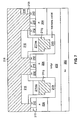
One embodiment of a trench MOSFET of the present invention is shown in partial cross section in FIG. 2. The trench MOSFET shown contains an N-type epitaxial layer 202, which is provided on an N+ substrate 200. The N+ substrate 200 is typically a silicon substrate having a thickness ranging, for example, from 10 to 25 mils and a resistivity ranging, for example, from 0.005 to 0.01 Ohm-cm. The N-type epitaxial layer 202 is also typically silicon having a thickness ranging from for example, 5 to 6 microns and a resistivity ranging, for example, from 0.18 to 0.25 Ohm-cm.
The thermally grown oxide regions 210 t typically range from 100 to 1000 Angstroms in thickness, while the deposited oxide regions 210 d typically range from 500 to 2000 Angstroms in thickness. In constructing a composite oxide region in this fashion, the trench MOSFET device can be provided with a very high cell density (e.g., 20M to 500M/in.sq.). The gate charges associated with this high cell density are held in check by providing thick oxide regions at the trench bottom, consisting of both thermally grown oxide regions 210 t and deposited oxide regions 210 d. As previously noted, the portions of the oxide regions at the trench bottoms 210 d, 210 t are not significantly involved in channel formation during operation and hence can be of considerable thickness, reducing gate charges. On the other hand, portions of the thermally grown gate oxide region 210 t along the trench sidewalls above the deposited oxide regions 210 d are sufficiently thin to effectively form a channel region within the adjacent P-body regions 204 during operation. Moreover, thermally grown oxide regions 210 t, rather than deposited oxide regions 210 d, are adjacent the silicon. As a result, the high state charge that is found at the interface between the silicon and the deposited oxide in prior art structures (e.g., the structure disclosed in the abstract of JP05335582) is avoided.
Within the epitaxial layer are P-body regions 204. Resistivities ranging from 0.1 to 1.0 Ohm-cm and depths of 1 to 2 microns from the surface of the epitaxial layer are typical of such structures. The trench MOSFET device of FIG. 2 also contains N+ source regions 212, which typically extend to a depth of 0.3 to 0.45 microns from the epitaxial layer surface and typically have resistivities of 0.001 to 0.003 Ohm-cm.
In the embodiment shown, P-body upper regions (p+ regions) 215 are provided between the n+ source regions 212 for purposes of forming good ohmic contact with the electrode 218. These regions 215 are shown as extending to approximately the same depth as the n+ source regions 212, but other depths are clearly possible. Resistivities of 0.002 to 0.005 Ohm-cm are typical.
Electrical contact is made with the n+ source regions 212 via metal source contact 218. Insulating regions 216, typically BPSG (borophosphosilicate glass), prevent the polysilicon regions 211 g associated with the gate electrodes from being shorted to the n+ source regions 212 through source contact 218. A separate metal gate contact (not shown) is typically connected to the gate runner portion of the polysilicon that is located outside of the region of the trench MOSFET cells. A metal drain contact (not shown) is also typically provided in electrical connection with the N+ substrate 200.
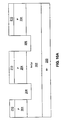
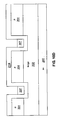
Another embodiment of the invention is shown in FIG. 3. FIG. 3 is essentially the same as FIG. 2, except for the configuration of the oxide regions lining the trenches. Specifically, whereas FIG. 2 contains oxide regions that are a combination of thermally grown oxide regions 210 t and deposited oxide regions 210 d, the oxide regions of FIG. 3 are entirely formed from thermally grown oxide 210 t. Nonetheless, as in FIG. 2, the oxide regions 210 t within the trenches 206 are thicker at the trench bottoms (typically 500 to 2000 Angstroms in thickness) than they are along the upper portions of the trench sidewalls (typically 100 to 1000 Angstroms). In this way, gate function is maintained, while reducing the gate charges associated with the device. Moreover, high interface state charges are avoided, because thermally grown oxide regions 210 t, rather deposited oxide regions, are placed adjacent the silicon.
Other embodiments of the invention are shown in FIG. 4 and FIG. 5. FIG. 4 and FIG. 5 are essentially the same as FIG. 2 and FIG. 3, respectively. However, the polysilicon gate regions 211 g of FIGS. 2 and 3 are replaced by composite gate regions consisting of both polysilicon gate regions 211 g and tungsten metal regions 211 m. These embodiments provide lower gate resistance relative to a device containing only polysilicon gate regions, improving switching frequency. In alternative embodiments, the tungsten metal is replaced by other refractory metals and metal alloys, such as titanium-tungsten alloys.
Still other related embodiments of the invention are shown in FIG. 6 and FIG. 7. FIG. 6 and FIG. 7 are essentially the same as FIG. 2 and FIG. 3, respectively, except that the polysilicon gate regions 211 g of FIGS. 2 and 3 are replaced by composite gate regions. In FIGS. 6 and 7, these regions consist of both polysilicon gate regions 211 g and refractory metal silicide regions 211 ms such as titanium silicide (typically TiSi2). Refractory metals that readily form silicides include titanium, tungsten, tantalum, and molybdenum.
An embodiment of a process for the manufacture of a device like that of FIG. 2 will now be described in connection with FIGS. 8A to 8G. In these figures, an N doped epitaxial layer 202 is initially grown on an N+ doped substrate 200. For example, epitaxial layer 202 can be 6.0 microns thick and have an n-type doping concentration of bout 3.4×1016 cm−3, while N+ doped substrate 200 can be 250 microns thick and have n-type doping concentration of about 5×1019 cm−3. A P-type layer 204 is then formed in the epitaxial layer 202 by implantation and diffusion. For example, the epitaxial layer 202 may be implanted with boron at 40 keV with a dosage of 6×1013 cm−2, followed by diffusion to a depth of 1.8 microns at 150° C.
A mask oxide layer (not shown) is then deposited, for example by chemical vapor deposition, and covered with a patterned trench mask (not shown). The mask oxide layer is then etched, for example, by buffered HF, forming a patterned mask oxide layer (not shown). Trenches 206 are subsequently etched through apertures in the patterned mask oxide layer, typically by reactive ion etching. Trench depths can be, for example, about 2.0 μm. Discrete P-body regions 204 are established as a result of this trench-forming step. A sacrificial oxide (not shown) is then grown, typically by dry oxidation to improve the quality of the silicon surface. This oxide is then removed, typically by buffered HF, forming the structure illustrated in FIG. 8A.
A thermal gate oxide layer 210 t is grown over the entire device, for example, by dry oxidation at 900 to 1150° C. A thickness in the range of 100 to 1000 Angstroms is preferred for the thermal gate oxide layer 210. Then, a TEOS (i.e., tetraethylorthosilicate or Si(OC2H5)4) layer 210 is deposited, for example, by PECVD (plasma enhanced chemical vapor deposition) at temperatures between 500 and 600° C., to provide the structure of FIG. 8B. The TEOS layer 210 typically ranges from 400 to 1000 Angstroms in thickness.
The surface of the structure is then covered, and the trenches are filled, with a photoresist layer 207 to provide the structure of FIG. 8C. The resist layer is then etched, for example, by reactive ion etching, until all of the photoresist is removed except for resist portions 207 at the bottom of the trenches, providing the structure of FIG. 8D. The TEOS layer 210 is then etched, for example, by buffered HF to produce the structure of FIG. 8E.
The remaining resist 207 is removed, for example, by sulfuric acid. Subsequently, the TEOS regions 210 are densified, for example, by annealing at 950° C. in N2 to provide high-density deposited silicon dioxide regions 210 d. The structure then undergoes an additional thermal oxidation step, for example, 10 to 20 minutes at 950 to 1150 C., to ensure that those portions of the gate oxide layer 210 t not covered by deposited oxide 210 d are of sufficient thickness. Thicknesses ranging from 10 to 1000 Angstroms are typical.
The surface of the structure is then covered, and the trenches are filled, with a polysilicon layer, typically using CVD. The polysilicon is typically doped N-type to reduce its resistivity, generally on order of 20 Ω/sq. N-type doping can be carried out, for example, during CVD with phosphorous chloride or by implantation with arsenic or phosphorous. As is typical, a patterned masking layer (not shown) is provided to preserve polysilicon in the gate runner region, and the unmasked portions of the polysilicon layer are etched, for example, by reactive ion etching. The polysilicon layer within the trench segments is slightly over-etched due to etching uniformity concerns, and the thus-formed polysilicon gate regions 211 g typically have top surfaces that are 0.1 to 0.2 microns below the adjacent surface of the epitaxial layer 204. The resulting structure is shown in FIG. 8F.
The oxide layer 210 t is then wet etched to a thickness of 100 Angstroms to form an implant oxide (not shown). The implant oxide avoids implant-channeling effects, implant damage, and heavy metal contamination during subsequent formation of source regions. Source regions 212 are formed within upper portions of the P-body regions 204 via an implantation and diffusion process, using a patterned masking layer (not shown). For example, the source regions 212 may be implanted with arsenic at a dosage of 1×1016 cm−2 and diffused to a depth of 0.4 microns at a temperature of 950° C. An additional mask (not shown) is then formed, followed by implantation and diffusion of boron to form P-body upper portions 215 (p+ regions) between n+ regions 212. For example, the P-body upper portions 215 may be implanted with boron at a dosage of 1.5e14 cm−2 and diffused to a depth of 0.3-0.6 microns.
A BPSG (borophosphosilicate glass) layer is then formed over the entire structure, for example, by PECVD, and provided with a patterned photoresist layer (not shown). The structure is etched, typically by reactive ion etching, to remove the BPSG and oxide over at least a portion of each source region 212, leaving behind BPSG regions 216. After removing the photoresist layer, the structure is provided with a metal contact layer 218 (aluminum in this example), which acts as a source electrode. The resulting cross-sectional views of this structure are shown in FIG. 8G. In the same step, a separate metal contact is typically connected to the gate runner, which is located outside the cells. Another metal contact is typically provided in connection with the substrate 200, which acts as a drain electrode.
An alternate method for producing a trench MOSFET structure like that shown in FIG. 2 is illustrated in FIGS. 9A through 9G. The process for producing the structure of FIG. 9A is the same as that set forth above in connection with FIG. 8A. The process for producing FIG. 9B is the same as FIG. 8B, except that the TEOS layer 210 is densified in FIG. 9B following deposition to provide a high-density silicon dioxide layer 210 d. As will become more apparent below, in contrast to the above procedure of FIGS. 8A through 8G, densification is performed at this earlier stage, because portions of the layer 210 d are permanently covered by polysilicon in the following step.
The surface of the structure is then covered, and the trenches are filled, with a doped polysilicon layer 211 g in a manner like that described in FIG. 8F above, resulting in the structure of FIG. 9C. The polysilicon layer is then etched, for example, by reactive ion etching, until only the bottoms of the trenches are filled with the polysilicon 211 g. The resulting structure is shown in FIG. 9D.
The densified silicon dioxide layer 210 d is then etched, for example by reactive ion etching, removing all of silicon dioxide layer 210 d, except where protected by the polysilicon 211 g coving the trench bottoms. The resulting structure is shown in FIG. 9E. As in FIG. 8F above, the structure then undergoes an additional thermal oxidation step to ensure that those portions of the gate oxide layer 210 t not covered by the deposited oxide 210 d are of sufficient thickness. An additional layer of polysilicon is then provided, covering the surface and filling the trenches of the device. As previously discussed, also in connection with FIG. 8F, a patterned masking layer is provided to preserve polysilicon in the gate runner region, and the polysilicon layer is slightly over-etched, creating final polysilicon gate regions 211 g within the trenches. The resulting structure is shown in FIG. 9F. Finally, the steps described above in connection with FIG. 8G are preformed, producing the device shown in FIG. 9G.
A method of producing a trench MOSFET structure like that shown in FIG. 3 will now be described in connection with FIGS. 10A through 10H.
As in the process of FIG. 8A, an N doped epitaxial layer 202 is initially grown on an N+ doped substrate 200. A P-type layer 204 is then formed in the epitaxial layer 202 by implantation and diffusion. A mask oxide layer is then deposited, and covered with a patterned trench mask (not shown). The mask oxide layer is then etched forming a patterned mask oxide layer 210. Trenches 206 are subsequently etched through apertures in the patterned mask oxide layer 210, establishing discrete P-body regions 204. The resulting structure is shown in FIG. 10A.
At this point, a thick oxide layer is grown over the entire structure, forming layer 210 t (which also includes the patterned mask oxide layer 210 from the prior step). The resulting structure is shown in FIG. 10B. The thick oxide layer is grown by thermal oxidation, for example, by either wet or dry oxidation at 950 to 1150° C. for a period of 10 to 120 minutes. After oxidation, the thick oxide layer is preferably 500 to 2000 microns in thickness.
The surface of the structure is then covered, and the trenches are filled, with a photoresist layer 207 to provide the structure of FIG. 10C. The resist layer is then etched, for example, by reactive ion etching, until all of the photoresist is removed except photoresist portions 207 at the bottom of the trenches, providing the structure of FIG. 10D.
The oxide layer 210 t is then etched, for example by reactive ion etching, removing all of thick oxide layer, except where it is protected by the photoresist covering the trench bottoms, resulting in distinct, thick thermally grown oxide regions 210 t as shown in FIG. 10E.
The remaining photoresist 207 is then removed, for example, by sulfuric acid. Subsequently, a thin gate oxide layer is formed on the exposed silicon surfaces of the structure, for example, by dry oxidation at 950 to 1150° C. This thin gate oxide layer is typically 100 to 1000 Angstroms in thickness. As shown in FIG. 10F, this oxidation step results in a thermally grown oxide layer 210 t having thick regions at the trench bottoms and thin regions on upper portions of the trench sidewalls (as well as on top of the structure).
A layer of polysilicon 211 g for the gate region is provided over the entire structure, covering the surface and filling the trenches of the device as shown in FIG. 10G. The device is completed from this point as discussed above in connection with FIGS. 8F and 8G, producing the structure of FIG. 10H.
A method of producing a trench MOSFET structure like that shown in FIG. 4 will now be described in connection with FIG. 11A and FIG. 11B.
This process is the same as that discussed above in connection with FIGS. 8A through FIG. 8E. At this point, the remaining resist is removed, the TEOS layer is densified to provide a high-density silicon dioxide layer 210 d, and the gate oxide layer 211 t is thickened as in FIG. 8F above. However, a substantially thinner polysilicon layer 211 g is provided over the surface of the device and in the trenches, such that the trenches are not filled by the polysilicon 211 g. Instead, trench filling is completed by depositing a metal layer 211 m of either tungsten (W) or a titanium-tungsten alloy (TiW) (or Tungsten Silicide (WSi), if desired) using techniques known in the art such as CVD. The resulting structure is shown in FIG. 11A
As above, a patterned masking layer is provided to preserve the polysilicon, as well as the W/TiW, in the gate runner region, and the layers of polysilicon 211 g and W/TiW 211 m are slightly over-etched, producing composite gate regions consisting of polysilicon 211 g and W/TiW 211 m. Finally, the steps described above in connection with FIG. 8G are preformed, producing the device of FIG. 11B.
A method of producing a trench MOSFET structure like that shown in FIG. 5 is now described in connection with FIG. 11C. This process is the same as that of FIGS. 10A through 10F. At this point, however, the trenches are not filled with polysilicon. Instead, a relatively thin polysilicon layer 211 g is provided over the surface of the device and in the trenches. The trenches are then filled by depositing a metal layer 211 m of either tungsten (W) or a titanium-tungsten alloy (TiW) (or Tungsten Silicide (WSi), if desired) and the structure is completed as discussed in connection with FIG. 11B. The completed structure is shown in FIG. 11C.
A method of producing a trench MOSFET structure like that shown in FIG. 6 is described in connection with FIG. 12A and FIG. 12B. The method is essentially the same as that discussed above in connection with FIGS. 8A through 8F, except that the polysilicon layer within the trench segment is more heavily over-etched, such that the polysilicon gate regions 211 g within the trenches typically have top surfaces that are 0.1 to 0.5 microns below the adjacent surface of the epitaxial layer 204. The patterned masking layer, which served to preserve polysilicon in the gate runner region, is removed and a refractory metal layer 211 m such as a titanium layer is deposited, for example, by sputtering, to produce the structure of FIG. 12A. The refractory metal is then alloyed with polysilicon in the trench by rapid thermal anneal, forming refractory metal silicide regions 211 ms (in this case titanium silicide (TiSi2)). The non reacted Ti portion on the oxide layer is removed after TiSi2 is formed in trench region. The steps described above in connection with FIG. 8G are then preformed, producing the device of FIG. 12B.
A method of producing a trench MOSFET structure like that shown in FIG. 7 is described in connection with FIG. 12C. The method is essentially the same as that discussed above in connection with FIG. 10A through FIG. 10G. After applying the patterned masking layer to preserve polysilicon in the gate runner region, the procedures discussed in connection with FIG. 12A and FIG. 12B above are followed, producing the structure of FIG. 12C.
Although various embodiments are specifically illustrated and described herein, it will be appreciated that modifications and variations of the present invention are covered by the above teachings and are within the purview of the appended claims without departing from the spirit and intended scope of the invention. As one example, the method of the present invention may be used to form a structure in which the conductivities of the various semiconductor regions are reversed from those described herein.
Claims (16)
1. A trench MOSFET device comprising:
a silicon substrate of a first conductivity type;
a silicon epitaxial layer of said first conductivity type over said substrate, said epitaxial layer having a lower majority carrier concentration than said substrate;
a body region of a second conductivity type within an upper portion of said epitaxial layer;
a trench extending into said epitaxial layer from an upper surface of said epitaxial layer, said trench extending through said body region, and said trench having trench sidewalls and a trench bottom;
an oxide region lining said trench, said oxide region comprising a lower segment covering at least the trench bottom and upper segments covering at least upper regions of said trench sidewalls;
a conductive region within said trench adjacent said oxide region; and
a source region of said first conductivity type within an upper portion of said body region and adjacent said trench,
wherein said lower segment of said oxide region is thicker than said upper segments of said oxide region such that shoulders are established in said oxide region adjacent said conductive region along said trench sidewalls, and
wherein said lower segment of said oxide region consists of two structurally distinct portions, a thermally grown portion adjacent said trench and a deposited oxide portion adjacent said conductive region and in contact with said thermally grown portion having different operational characteristics than said deposited oxide portion, and wherein said upper segments of said oxide region consists of thermally grown oxide.
2. The trench MOSFET device of claim 1 , wherein said deposited oxide portion is densified TEOS.
3. The trench MOSFET device of claim 1 , wherein said thermally grown portion ranges from 500to 2000 Angstroms in thickness.
4. The trench MOSFET device of claim 1 , wherein said deposited oxide portion ranges from 500 to 2000 Angstroms in thickness.
5. The trench MOSFET device of claim 1 , wherein said upper segment of said oxide region ranges from 100 to 1000 Angstroms in thickness.
6. The trench MOSFET device of claim 1 , wherein said lower segment of said oxide region is a thick thermally grown oxide region, and wherein said upper segments of said oxide region are thin thermally grown oxide regions.
7. The trench MOSFET device of claim 6 , wherein said thick thermally grown oxide region ranges from 500 to 2000 Angstroms in thickness.
8. The trench MOSFET device of claim 6 , wherein said thin thermally grown oxide region ranges from 100 to 1000 Angstroms in thickness.
9. The trench MOSFET device of claim 1 , wherein the conductive region comprises polycrystalline silicon.
10. The trench MOSFET device of claim 1 , wherein the conductive region comprises a polycrystalline silicon portion and a portion selected from a refractory metal and a refractory metal alloy.
11. The trench MOSFET device of claim 10 , wherein the conductive region comprises a polycrystalline silicon portion and a tungsten portion.
12. The trench MOSFET device of claim 10 , wherein the conductive region comprises a polycrystalline silicon portion and a titanium-tungsten alloy portion.
13. The trench MOSFET device of claim 1 , wherein the conductive region comprises a polycrystalline silicon portion and a refractory metal silicide portion.
14. The trench MOSFET device of claim 13 , wherein the conductive region comprises a polycrystalline silicon portion and a titanium silicide portion.
15. The trench MOSFET device of claim 1 , wherein said first conductivity type is N-type conductivity and said second conductivity type is P-type conductivity.
16. A trench MOSFET device comprising:
a silicon substrate of a first conductivity type;
a silicon epitaxial layer of said first conductivity type over said substrate, said epitaxial layer having a lower majority carrier concentration than said substrate;
a body region of a second conductivity type within an upper portion of said epitaxial layer;
a trench extending into said epitaxial layer from an upper surface of said epitaxial layer, said trench extending through said body region, and said trench having trench sidewalls and a trench bottom;
an oxide region lining said trench, said oxide region comprising a u-shaped lower segment covering the trench bottom and lower regions of said trench sidewalls and upper segments covering upper regions of said trench sidewalls, wherein said lower segment of said oxide region is thicker than said upper segments;
a conductive region within said trench adjacent said oxide region; and
a source region of said first conductivity type within an upper portion of said body region and adjacent said trench, and
wherein said lower segment of said oxide region consists of two structurally distinct portions, a thermally grown portion adjacent said trench and a deposited oxide portion adjacent said conductive region and in contact with, said thermally grown portion having different operational characteristics than said deposited oxide portion, and wherein said upper segments of said oxide region consists of thermally grown oxide.
Priority Applications (9)
| Application Number | Priority Date | Filing Date | Title |
|---|---|---|---|
| US10/002,529 US6674124B2 (en) | 2001-11-15 | 2001-11-15 | Trench MOSFET having low gate charge |
| TW091133164A TW200300295A (en) | 2001-11-15 | 2002-11-12 | Trench MOSFET having low gate charge |
| CNB028226496A CN100392866C (en) | 2001-11-15 | 2002-11-13 | Trench MOSFET having low gate charge |
| PCT/US2002/036517 WO2003044865A1 (en) | 2001-11-15 | 2002-11-13 | Trench mosfet having low gate charge |
| KR1020047007408A KR100936966B1 (en) | 2001-11-15 | 2002-11-13 | Trench mosfet device having low gate charge and method of forming the same |
| AU2002350184A AU2002350184A1 (en) | 2001-11-15 | 2002-11-13 | Trench mosfet having low gate charge |
| JP2003546406A JP5081367B2 (en) | 2001-11-15 | 2002-11-13 | Trench metal oxide semiconductor field effect transistor device with low gate charge and method for manufacturing the same. |
| EP02786713A EP1451877A4 (en) | 2001-11-15 | 2002-11-13 | Trench mosfet having low gate charge |
| US10/751,687 US6979621B2 (en) | 2001-11-15 | 2004-01-05 | Trench MOSFET having low gate charge |
Applications Claiming Priority (1)
| Application Number | Priority Date | Filing Date | Title |
|---|---|---|---|
| US10/002,529 US6674124B2 (en) | 2001-11-15 | 2001-11-15 | Trench MOSFET having low gate charge |
Related Child Applications (1)
| Application Number | Title | Priority Date | Filing Date |
|---|---|---|---|
| US10/751,687 Division US6979621B2 (en) | 2001-11-15 | 2004-01-05 | Trench MOSFET having low gate charge |
Publications (2)
| Publication Number | Publication Date |
|---|---|
| US20030089946A1 US20030089946A1 (en) | 2003-05-15 |
| US6674124B2 true US6674124B2 (en) | 2004-01-06 |
Family
ID=21701190
Family Applications (2)
| Application Number | Title | Priority Date | Filing Date |
|---|---|---|---|
| US10/002,529 Expired - Lifetime US6674124B2 (en) | 2001-11-15 | 2001-11-15 | Trench MOSFET having low gate charge |
| US10/751,687 Expired - Lifetime US6979621B2 (en) | 2001-11-15 | 2004-01-05 | Trench MOSFET having low gate charge |
Family Applications After (1)
| Application Number | Title | Priority Date | Filing Date |
|---|---|---|---|
| US10/751,687 Expired - Lifetime US6979621B2 (en) | 2001-11-15 | 2004-01-05 | Trench MOSFET having low gate charge |
Country Status (8)
| Country | Link |
|---|---|
| US (2) | US6674124B2 (en) |
| EP (1) | EP1451877A4 (en) |
| JP (1) | JP5081367B2 (en) |
| KR (1) | KR100936966B1 (en) |
| CN (1) | CN100392866C (en) |
| AU (1) | AU2002350184A1 (en) |
| TW (1) | TW200300295A (en) |
| WO (1) | WO2003044865A1 (en) |
Cited By (22)
| Publication number | Priority date | Publication date | Assignee | Title |
|---|---|---|---|---|
| US20020137322A1 (en) * | 2001-03-21 | 2002-09-26 | International Rectifier Corp. | Reduced mask count process for manufacture of mosgated device |
| US20020153558A1 (en) * | 2001-04-02 | 2002-10-24 | Toshiyuki Takemori | Semiconductor device and method for manufacturing the same |
| US20040038467A1 (en) * | 2001-07-03 | 2004-02-26 | Siliconix Incorporated | Trench MIS device having implanted drain-drift region and thick bottom oxide and process for manufacturing the same |
| US20040150038A1 (en) * | 2001-11-15 | 2004-08-05 | Fwu-Iuan Hshieh | Trench MOSFET having low gate charge |
| US20040173839A1 (en) * | 2003-03-06 | 2004-09-09 | Daniele Casarotto | Nonvolatile memory cell |
| US20040203217A1 (en) * | 2003-04-11 | 2004-10-14 | Mosel Vitelic, Inc. | Bottom oxide formation process for preventing formation of voids in trench |
| US20050023611A1 (en) * | 2003-07-31 | 2005-02-03 | Karsten Wieczorek | Field effect transistor having a doped gate electrode with reduced gate depletion and method of forming the transistor |
| US20050037559A1 (en) * | 2003-08-01 | 2005-02-17 | Jun Osanai | Method of manufacturing a semiconductor device |
| US20050236665A1 (en) * | 2001-07-03 | 2005-10-27 | Darwish Mohamed N | Trench MIS device having implanted drain-drift region and thick bottom oxide and process for manufacturing the same |
| US20060038223A1 (en) * | 2001-07-03 | 2006-02-23 | Siliconix Incorporated | Trench MOSFET having drain-drift region comprising stack of implanted regions |
| US20060113588A1 (en) * | 2004-11-29 | 2006-06-01 | Sillicon-Based Technology Corp. | Self-aligned trench-type DMOS transistor structure and its manufacturing methods |
| US20060121676A1 (en) * | 2001-07-03 | 2006-06-08 | Siliconix Incorporated | Trench MIS device with thick oxide layer in bottom of gate contact trench |
| US20080150021A1 (en) * | 2004-03-10 | 2008-06-26 | Nxp B.V. | Trench-Gate Transistors and Their Manufacture |
| US20080185642A1 (en) * | 2004-10-29 | 2008-08-07 | International Rectifier Corporation | Trench MOSFET with deposited oxide |
| US20090114999A1 (en) * | 2004-03-05 | 2009-05-07 | Samsung Electroncs Co., Ltd. | Transistors of semiconductor device having channel region in a channel-portion hole and methods of forming the same |
| US20090206395A1 (en) * | 2008-02-20 | 2009-08-20 | Force-Mos Technology Corporation | Trench mosfet with double epitaxial structure |
| US20110095302A1 (en) * | 2009-10-26 | 2011-04-28 | Mitsubishi Electric Corporation | Semiconductor device and manufacturing method thereof |
| CN102082097A (en) * | 2009-11-09 | 2011-06-01 | 凹凸电子(武汉)有限公司 | Trench metal oxide semiconductor field effect transistor, a method for fabricating same and power conversion system |
| US8492226B2 (en) * | 2011-09-21 | 2013-07-23 | Globalfoundries Singapore Pte. Ltd. | Trench transistor |
| US8802530B2 (en) * | 2012-06-06 | 2014-08-12 | Alpha And Omega Semiconductor Incorporated | MOSFET with improved performance through induced net charge region in thick bottom insulator |
| US20160351665A1 (en) * | 2015-05-27 | 2016-12-01 | Toyota Jidosha Kabushiki Kaisha | Semiconductor device |
| US9570545B2 (en) | 2011-09-21 | 2017-02-14 | Globalfoundries Singapore Pte. Ltd. | High voltage trench transistor |
Families Citing this family (54)
| Publication number | Priority date | Publication date | Assignee | Title |
|---|---|---|---|---|
| JP5008247B2 (en) * | 2003-04-03 | 2012-08-22 | セイコーインスツル株式会社 | Manufacturing method of vertical MOS transistor |
| JP4346433B2 (en) * | 2003-12-24 | 2009-10-21 | Okiセミコンダクタ株式会社 | Manufacturing method of semiconductor device |
| US7372088B2 (en) * | 2004-01-27 | 2008-05-13 | Matsushita Electric Industrial Co., Ltd. | Vertical gate semiconductor device and method for fabricating the same |
| JP4091921B2 (en) * | 2004-02-16 | 2008-05-28 | 松下電器産業株式会社 | Semiconductor device and manufacturing method thereof |
| JP4500598B2 (en) * | 2004-06-24 | 2010-07-14 | トヨタ自動車株式会社 | Insulated gate type semiconductor device manufacturing method |
| KR100730466B1 (en) * | 2005-12-29 | 2007-06-19 | 매그나칩 반도체 유한회사 | Trench transistor and method for manufacturing the same |
| JP4622905B2 (en) * | 2006-03-24 | 2011-02-02 | トヨタ自動車株式会社 | Method of manufacturing insulated gate semiconductor device |
| JP4748070B2 (en) * | 2007-01-26 | 2011-08-17 | トヨタ自動車株式会社 | Manufacturing method of semiconductor substrate |
| JP5183959B2 (en) * | 2007-04-23 | 2013-04-17 | 新日本無線株式会社 | Method for manufacturing MOSFET type semiconductor device |
| KR100853799B1 (en) * | 2007-07-25 | 2008-08-25 | 주식회사 동부하이텍 | Trench gate semi-conductor device, and method for fabricating thereof |
| DE102007037858B4 (en) | 2007-08-10 | 2012-04-19 | Infineon Technologies Ag | Semiconductor device with improved dynamic behavior |
| JP2009088188A (en) * | 2007-09-28 | 2009-04-23 | Sanyo Electric Co Ltd | Trench gate type transistor and method for manufacturing same |
| US8076720B2 (en) * | 2007-09-28 | 2011-12-13 | Semiconductor Components Industries, Llc | Trench gate type transistor |
| US20090098701A1 (en) * | 2007-10-15 | 2009-04-16 | Jurgen Faul | Method of manufacturing an integrated circuit |
| TW200921912A (en) * | 2007-11-05 | 2009-05-16 | Anpec Electronics Corp | Power transistor capable of decreasing capacitance between gate and drain |
| KR100970282B1 (en) * | 2007-11-19 | 2010-07-15 | 매그나칩 반도체 유한회사 | Trench MOSFET and Manufacturing Method thereof |
| US8664747B2 (en) * | 2008-04-28 | 2014-03-04 | Toshiba Techno Center Inc. | Trenched substrate for crystal growth and wafer bonding |
| US8901638B2 (en) * | 2008-07-25 | 2014-12-02 | Nxp B.V. | Trench-gate semiconductor device |
| US8193081B2 (en) * | 2009-10-20 | 2012-06-05 | Taiwan Semiconductor Manufacturing Company, Ltd. | Method and system for metal gate formation with wider metal gate fill margin |
| US20110115019A1 (en) * | 2009-11-13 | 2011-05-19 | Maxim Integrated Products, Inc. | Cmos compatible low gate charge lateral mosfet |
| US8969958B1 (en) | 2009-11-13 | 2015-03-03 | Maxim Integrated Products, Inc. | Integrated MOS power transistor with body extension region for poly field plate depletion assist |
| US8946851B1 (en) | 2009-11-13 | 2015-02-03 | Maxim Integrated Products, Inc. | Integrated MOS power transistor with thin gate oxide and low gate charge |
| US20110115018A1 (en) * | 2009-11-13 | 2011-05-19 | Maxim Integrated Products, Inc. | Mos power transistor |
| US8987818B1 (en) | 2009-11-13 | 2015-03-24 | Maxim Integrated Products, Inc. | Integrated MOS power transistor with thin gate oxide and low gate charge |
| US8963241B1 (en) | 2009-11-13 | 2015-02-24 | Maxim Integrated Products, Inc. | Integrated MOS power transistor with poly field plate extension for depletion assist |
| WO2011148427A1 (en) | 2010-05-27 | 2011-12-01 | Fuji Electric Co., Ltd. | Mos-driven semiconductor device and method for manufacturing mos-driven semiconductor device |
| US8349653B2 (en) | 2010-06-02 | 2013-01-08 | Maxim Integrated Products, Inc. | Use of device assembly for a generalization of three-dimensional metal interconnect technologies |
| US10672748B1 (en) | 2010-06-02 | 2020-06-02 | Maxim Integrated Products, Inc. | Use of device assembly for a generalization of three-dimensional heterogeneous technologies integration |
| CN102569428B (en) * | 2010-12-21 | 2015-06-03 | 上海华虹宏力半导体制造有限公司 | Longitudinal voltage-controlled varactor and preparation method thereof |
| CN102623316A (en) * | 2011-01-27 | 2012-08-01 | 无锡华润上华半导体有限公司 | Methods for preparing groove bottom auxiliary gate dielectric layer and groove DMOS pipe |
| JP5395309B2 (en) * | 2011-03-23 | 2014-01-22 | パナソニック株式会社 | Semiconductor device and manufacturing method thereof |
| JP5637916B2 (en) * | 2011-03-31 | 2014-12-10 | トヨタ自動車株式会社 | Semiconductor device and manufacturing method thereof |
| JP5358653B2 (en) * | 2011-11-15 | 2013-12-04 | セミコンダクター・コンポーネンツ・インダストリーズ・リミテッド・ライアビリティ・カンパニー | Manufacturing method of trench gate type transistor |
| US8946002B2 (en) * | 2012-07-24 | 2015-02-03 | Semiconductor Components Industries, Llc | Method of forming a semiconductor device having a patterned gate dielectric and structure therefor |
| CN102800704A (en) * | 2012-08-29 | 2012-11-28 | 上海宏力半导体制造有限公司 | Trench MOS (Metal Oxide Semiconductor) transistor and manufacture method thereof, and integrated circuit |
| KR101779384B1 (en) * | 2013-03-05 | 2017-09-19 | 매그나칩 반도체 유한회사 | Method for fabricating semiconductor device |
| KR101832334B1 (en) * | 2013-03-05 | 2018-02-27 | 매그나칩 반도체 유한회사 | Semiconductor device and method for fabricating the same |
| US8748976B1 (en) * | 2013-03-06 | 2014-06-10 | Texas Instruments Incorporated | Dual RESURF trench field plate in vertical MOSFET |
| JP2014207403A (en) * | 2013-04-16 | 2014-10-30 | 住友電気工業株式会社 | Silicon carbide semiconductor device manufacturing method |
| JP6131689B2 (en) | 2013-04-16 | 2017-05-24 | 住友電気工業株式会社 | Method for manufacturing silicon carbide semiconductor device |
| CN104347708A (en) * | 2013-08-07 | 2015-02-11 | 中芯国际集成电路制造(北京)有限公司 | Multi-grid VDMOS (vertical double-diffused metal oxide semiconductor) transistor and forming method thereof |
| CN106684126A (en) * | 2016-12-12 | 2017-05-17 | 中航(重庆)微电子有限公司 | Trench type transistor device structure and making method |
| JP2018181911A (en) * | 2017-04-04 | 2018-11-15 | 浜松ホトニクス株式会社 | Optical semiconductor device |
| US10720358B2 (en) | 2017-06-30 | 2020-07-21 | Taiwan Semiconductor Manufacturing Co., Ltd. | Semiconductor device having a liner layer with a configured profile and method of fabricating thereof |
| DE102018104944A1 (en) | 2017-06-30 | 2019-01-03 | Taiwan Semiconductor Manufacturing Co., Ltd. | Semiconductor device having a liner layer with a configured profile and method of making the same |
| CN107706101A (en) | 2017-09-29 | 2018-02-16 | 上海华虹宏力半导体制造有限公司 | The manufacture method of trench gate |
| WO2019178765A1 (en) * | 2018-03-21 | 2019-09-26 | Texas Instruments Incorporated | Semiconductor device having polysilicon field plate for power mosfets |
| DE102019109368A1 (en) * | 2018-05-15 | 2019-11-21 | Infineon Technologies Ag | SEMICONDUCTOR DEVICE WITH SILICON CARBIDE BODY AND MANUFACTURING METHOD |
| KR102505229B1 (en) | 2018-10-02 | 2023-03-06 | 삼성전자주식회사 | Semiconductor device and method of fabricating semiconductor device |
| US10950699B2 (en) | 2019-08-05 | 2021-03-16 | Vishay-Siliconix, LLC | Termination for vertical trench shielded devices |
| CN112750897A (en) * | 2019-10-29 | 2021-05-04 | 华润微电子(重庆)有限公司 | Groove type field effect transistor structure and preparation method thereof |
| CN111370473A (en) * | 2020-03-24 | 2020-07-03 | 成都森未科技有限公司 | Groove type device and preparation method thereof |
| US20220320310A1 (en) * | 2020-06-18 | 2022-10-06 | Dynex Semiconductor Limited | Method of forming asymmetric thickness oxide trenches |
| CN112185893A (en) * | 2020-09-29 | 2021-01-05 | 深圳市芯电元科技有限公司 | Manufacturing method of trench MOSFET |
Citations (14)
| Publication number | Priority date | Publication date | Assignee | Title |
|---|---|---|---|---|
| US5072266A (en) | 1988-12-27 | 1991-12-10 | Siliconix Incorporated | Trench DMOS power transistor with field-shaping body profile and three-dimensional geometry |
| JPH05335582A (en) | 1992-05-27 | 1993-12-17 | Omron Corp | Vertical mosfet device and manufacture thereof |
| US5442214A (en) * | 1994-08-09 | 1995-08-15 | United Microelectronics Corp. | VDMOS transistor and manufacturing method therefor |
| US5541425A (en) | 1994-01-20 | 1996-07-30 | Mitsubishi Denki Kabushiki Kaisha | Semiconductor device having trench structure |
| US5637898A (en) * | 1995-12-22 | 1997-06-10 | North Carolina State University | Vertical field effect transistors having improved breakdown voltage capability and low on-state resistance |
| US5801417A (en) * | 1988-05-17 | 1998-09-01 | Advanced Power Technology, Inc. | Self-aligned power MOSFET device with recessed gate and source |
| US5866931A (en) | 1993-04-14 | 1999-02-02 | Siliconix Incorporated | DMOS power transistor with reduced number of contacts using integrated body-source connections |
| US5907776A (en) | 1997-07-11 | 1999-05-25 | Magepower Semiconductor Corp. | Method of forming a semiconductor structure having reduced threshold voltage and high punch-through tolerance |
| US20010000919A1 (en) * | 1999-05-19 | 2001-05-10 | Harris Corporation | MOS-gated power device having extended trench and doping zone and process for forming same |
| US6252277B1 (en) * | 1999-09-09 | 2001-06-26 | Chartered Semiconductor Manufacturing Ltd. | Embedded polysilicon gate MOSFET |
| US6274905B1 (en) * | 1999-06-30 | 2001-08-14 | Fairchild Semiconductor Corporation | Trench structure substantially filled with high-conductivity material |
| US20010028085A1 (en) * | 1999-03-01 | 2001-10-11 | Blanchard Richard A. | Trench DMOS transistor structure having a low resistance path to a drain contact located on an upper surface |
| US6388286B1 (en) * | 1998-10-26 | 2002-05-14 | North Carolina State University | Power semiconductor devices having trench-based gate electrodes and field plates |
| US6404007B1 (en) * | 1999-04-05 | 2002-06-11 | Fairchild Semiconductor Corporation | Trench transistor with superior gate dielectric |
Family Cites Families (12)
| Publication number | Priority date | Publication date | Assignee | Title |
|---|---|---|---|---|
| JPH09181304A (en) * | 1995-12-21 | 1997-07-11 | Toyota Motor Corp | Semiconductor device and its manufacture |
| US5770878A (en) * | 1996-04-10 | 1998-06-23 | Harris Corporation | Trench MOS gate device |
| JP3502531B2 (en) * | 1997-08-28 | 2004-03-02 | 株式会社ルネサステクノロジ | Method for manufacturing semiconductor device |
| US6262453B1 (en) * | 1998-04-24 | 2001-07-17 | Magepower Semiconductor Corp. | Double gate-oxide for reducing gate-drain capacitance in trenched DMOS with high-dopant concentration buried-region under trenched gate |
| US6291298B1 (en) * | 1999-05-25 | 2001-09-18 | Advanced Analogic Technologies, Inc. | Process of manufacturing Trench gate semiconductor device having gate oxide layer with multiple thicknesses |
| JP2001036078A (en) * | 1999-07-22 | 2001-02-09 | Seiko Epson Corp | Mos-type transistor and manufacture thereof |
| GB9917099D0 (en) * | 1999-07-22 | 1999-09-22 | Koninkl Philips Electronics Nv | Cellular trench-gate field-effect transistors |
| DE19935442C1 (en) * | 1999-07-28 | 2000-12-21 | Siemens Ag | Power trench-metal oxide semiconductor transistor is produced using a temporary layer to allow formation of a trench insulating film which is thicker at the trench lower end than at the trench upper end |
| JP2001345444A (en) * | 1999-10-25 | 2001-12-14 | Seiko Instruments Inc | Semiconductor device and its manufacturing method |
| US6312993B1 (en) * | 2000-02-29 | 2001-11-06 | General Semiconductor, Inc. | High speed trench DMOS |
| GB0010041D0 (en) * | 2000-04-26 | 2000-06-14 | Koninkl Philips Electronics Nv | Trench semiconductor device manufacture |
| US6674124B2 (en) * | 2001-11-15 | 2004-01-06 | General Semiconductor, Inc. | Trench MOSFET having low gate charge |
-
2001
- 2001-11-15 US US10/002,529 patent/US6674124B2/en not_active Expired - Lifetime
-
2002
- 2002-11-12 TW TW091133164A patent/TW200300295A/en unknown
- 2002-11-13 EP EP02786713A patent/EP1451877A4/en not_active Withdrawn
- 2002-11-13 JP JP2003546406A patent/JP5081367B2/en not_active Expired - Fee Related
- 2002-11-13 CN CNB028226496A patent/CN100392866C/en not_active Expired - Fee Related
- 2002-11-13 WO PCT/US2002/036517 patent/WO2003044865A1/en active Application Filing
- 2002-11-13 AU AU2002350184A patent/AU2002350184A1/en not_active Abandoned
- 2002-11-13 KR KR1020047007408A patent/KR100936966B1/en active IP Right Grant
-
2004
- 2004-01-05 US US10/751,687 patent/US6979621B2/en not_active Expired - Lifetime
Patent Citations (14)
| Publication number | Priority date | Publication date | Assignee | Title |
|---|---|---|---|---|
| US5801417A (en) * | 1988-05-17 | 1998-09-01 | Advanced Power Technology, Inc. | Self-aligned power MOSFET device with recessed gate and source |
| US5072266A (en) | 1988-12-27 | 1991-12-10 | Siliconix Incorporated | Trench DMOS power transistor with field-shaping body profile and three-dimensional geometry |
| JPH05335582A (en) | 1992-05-27 | 1993-12-17 | Omron Corp | Vertical mosfet device and manufacture thereof |
| US5866931A (en) | 1993-04-14 | 1999-02-02 | Siliconix Incorporated | DMOS power transistor with reduced number of contacts using integrated body-source connections |
| US5541425A (en) | 1994-01-20 | 1996-07-30 | Mitsubishi Denki Kabushiki Kaisha | Semiconductor device having trench structure |
| US5442214A (en) * | 1994-08-09 | 1995-08-15 | United Microelectronics Corp. | VDMOS transistor and manufacturing method therefor |
| US5637898A (en) * | 1995-12-22 | 1997-06-10 | North Carolina State University | Vertical field effect transistors having improved breakdown voltage capability and low on-state resistance |
| US5907776A (en) | 1997-07-11 | 1999-05-25 | Magepower Semiconductor Corp. | Method of forming a semiconductor structure having reduced threshold voltage and high punch-through tolerance |
| US6388286B1 (en) * | 1998-10-26 | 2002-05-14 | North Carolina State University | Power semiconductor devices having trench-based gate electrodes and field plates |
| US20010028085A1 (en) * | 1999-03-01 | 2001-10-11 | Blanchard Richard A. | Trench DMOS transistor structure having a low resistance path to a drain contact located on an upper surface |
| US6404007B1 (en) * | 1999-04-05 | 2002-06-11 | Fairchild Semiconductor Corporation | Trench transistor with superior gate dielectric |
| US20010000919A1 (en) * | 1999-05-19 | 2001-05-10 | Harris Corporation | MOS-gated power device having extended trench and doping zone and process for forming same |
| US6274905B1 (en) * | 1999-06-30 | 2001-08-14 | Fairchild Semiconductor Corporation | Trench structure substantially filled with high-conductivity material |
| US6252277B1 (en) * | 1999-09-09 | 2001-06-26 | Chartered Semiconductor Manufacturing Ltd. | Embedded polysilicon gate MOSFET |
Non-Patent Citations (1)
| Title |
|---|
| Hsing-Huang Tseng et al., "A Robust Gate Dielectric for Submicron Technology," Semiconductor International, Jul. 1992, pp. 68-72. |
Cited By (45)
| Publication number | Priority date | Publication date | Assignee | Title |
|---|---|---|---|---|
| US6893923B2 (en) * | 2001-03-21 | 2005-05-17 | International Rectifier Corporation | Reduced mask count process for manufacture of mosgated device |
| US20020137322A1 (en) * | 2001-03-21 | 2002-09-26 | International Rectifier Corp. | Reduced mask count process for manufacture of mosgated device |
| US6809375B2 (en) * | 2001-04-02 | 2004-10-26 | Shindengen Electric Manufacturing Co., Ltd. | Semiconductor device having shallow trenches and method for manufacturing the same |
| US7397082B2 (en) | 2001-04-02 | 2008-07-08 | Shindengen Electric Manufacturing Co., Ltd. | Semiconductor device having shallow trenches and method for manufacturing the same |
| US20050017294A1 (en) * | 2001-04-02 | 2005-01-27 | Shindengen Electric Manufacturing Co., Ltd. | Semiconductor device having shallow trenches and method for manufacturing the same |
| US20020153558A1 (en) * | 2001-04-02 | 2002-10-24 | Toshiyuki Takemori | Semiconductor device and method for manufacturing the same |
| US20060038223A1 (en) * | 2001-07-03 | 2006-02-23 | Siliconix Incorporated | Trench MOSFET having drain-drift region comprising stack of implanted regions |
| US7435650B2 (en) | 2001-07-03 | 2008-10-14 | Siliconix Incorporated | Process for manufacturing trench MIS device having implanted drain-drift region and thick bottom oxide |
| US7416947B2 (en) | 2001-07-03 | 2008-08-26 | Siliconix Incorporated | Method of fabricating trench MIS device with thick oxide layer in bottom of trench |
| US20040227182A1 (en) * | 2001-07-03 | 2004-11-18 | Siliconix Incorporated | Process for manufacturing trench MIS device having implanted drain-drift region and thick botton oxide |
| US7326995B2 (en) | 2001-07-03 | 2008-02-05 | Siliconix Incorporated | Trench MIS device having implanted drain-drift region and thick bottom oxide |
| US7291884B2 (en) * | 2001-07-03 | 2007-11-06 | Siliconix Incorporated | Trench MIS device having implanted drain-drift region and thick bottom oxide |
| US20040038467A1 (en) * | 2001-07-03 | 2004-02-26 | Siliconix Incorporated | Trench MIS device having implanted drain-drift region and thick bottom oxide and process for manufacturing the same |
| US20050236665A1 (en) * | 2001-07-03 | 2005-10-27 | Darwish Mohamed N | Trench MIS device having implanted drain-drift region and thick bottom oxide and process for manufacturing the same |
| US20060121676A1 (en) * | 2001-07-03 | 2006-06-08 | Siliconix Incorporated | Trench MIS device with thick oxide layer in bottom of gate contact trench |
| US6979621B2 (en) * | 2001-11-15 | 2005-12-27 | General Semiconductor, Inc. | Trench MOSFET having low gate charge |
| US20040150038A1 (en) * | 2001-11-15 | 2004-08-05 | Fwu-Iuan Hshieh | Trench MOSFET having low gate charge |
| US20040173839A1 (en) * | 2003-03-06 | 2004-09-09 | Daniele Casarotto | Nonvolatile memory cell |
| US6873003B2 (en) * | 2003-03-06 | 2005-03-29 | Infineon Technologies Aktiengesellschaft | Nonvolatile memory cell |
| US6974749B2 (en) * | 2003-04-11 | 2005-12-13 | Mosel Vitelic, Inc. | Bottom oxide formation process for preventing formation of voids in trench |
| US20040203217A1 (en) * | 2003-04-11 | 2004-10-14 | Mosel Vitelic, Inc. | Bottom oxide formation process for preventing formation of voids in trench |
| US20050023611A1 (en) * | 2003-07-31 | 2005-02-03 | Karsten Wieczorek | Field effect transistor having a doped gate electrode with reduced gate depletion and method of forming the transistor |
| US7494872B2 (en) * | 2003-07-31 | 2009-02-24 | Advanced Micro Devices, Inc. | Field effect transistor having a doped gate electrode with reduced gate depletion and method of forming the transistor |
| US20050037559A1 (en) * | 2003-08-01 | 2005-02-17 | Jun Osanai | Method of manufacturing a semiconductor device |
| US6972232B2 (en) * | 2003-08-01 | 2005-12-06 | Seiko Instruments Inc. | Method of manufacturing a semiconductor device |
| US7696570B2 (en) * | 2004-03-05 | 2010-04-13 | Samsung Electronics Co., Ltd. | Transistors of semiconductor device having channel region in a channel-portion hole and methods of forming the same |
| US20090114999A1 (en) * | 2004-03-05 | 2009-05-07 | Samsung Electroncs Co., Ltd. | Transistors of semiconductor device having channel region in a channel-portion hole and methods of forming the same |
| US20080150021A1 (en) * | 2004-03-10 | 2008-06-26 | Nxp B.V. | Trench-Gate Transistors and Their Manufacture |
| US8222693B2 (en) | 2004-03-10 | 2012-07-17 | Nxp B.V. | Trench-gate transistors and their manufacture |
| US8106446B2 (en) * | 2004-10-29 | 2012-01-31 | International Rectifier Corporation | Trench MOSFET with deposited oxide |
| US20080185642A1 (en) * | 2004-10-29 | 2008-08-07 | International Rectifier Corporation | Trench MOSFET with deposited oxide |
| US20060113588A1 (en) * | 2004-11-29 | 2006-06-01 | Sillicon-Based Technology Corp. | Self-aligned trench-type DMOS transistor structure and its manufacturing methods |
| US20090206395A1 (en) * | 2008-02-20 | 2009-08-20 | Force-Mos Technology Corporation | Trench mosfet with double epitaxial structure |
| US8159021B2 (en) * | 2008-02-20 | 2012-04-17 | Force-Mos Technology Corporation | Trench MOSFET with double epitaxial structure |
| US8723254B2 (en) * | 2009-10-26 | 2014-05-13 | Mitsubishi Electric Corporation | Semiconductor device and manufacturing method thereof |
| US20110095302A1 (en) * | 2009-10-26 | 2011-04-28 | Mitsubishi Electric Corporation | Semiconductor device and manufacturing method thereof |
| CN102082097A (en) * | 2009-11-09 | 2011-06-01 | 凹凸电子(武汉)有限公司 | Trench metal oxide semiconductor field effect transistor, a method for fabricating same and power conversion system |
| CN102082097B (en) * | 2009-11-09 | 2013-07-31 | 凹凸电子(武汉)有限公司 | Trench metal oxide semiconductor field effect transistor, a method for fabricating same and power conversion system |
| US8492226B2 (en) * | 2011-09-21 | 2013-07-23 | Globalfoundries Singapore Pte. Ltd. | Trench transistor |
| US8786013B2 (en) | 2011-09-21 | 2014-07-22 | Globalfoundries Singapore Pte. Ltd. | Trench transistor |
| US9570545B2 (en) | 2011-09-21 | 2017-02-14 | Globalfoundries Singapore Pte. Ltd. | High voltage trench transistor |
| US8802530B2 (en) * | 2012-06-06 | 2014-08-12 | Alpha And Omega Semiconductor Incorporated | MOSFET with improved performance through induced net charge region in thick bottom insulator |
| TWI496293B (en) * | 2012-06-06 | 2015-08-11 | Alpha & Omega Semiconductor | Mosfet element and method for manufacturing mosfet element |
| US20160351665A1 (en) * | 2015-05-27 | 2016-12-01 | Toyota Jidosha Kabushiki Kaisha | Semiconductor device |
| US10068972B2 (en) * | 2015-05-27 | 2018-09-04 | Toyota Jidosha Kabushiki Kaisha | Semiconductor device with opposite conductivity-type impurity regions between source and trench gate for reducing leakage |
Also Published As
| Publication number | Publication date |
|---|---|
| TW200300295A (en) | 2003-05-16 |
| US20030089946A1 (en) | 2003-05-15 |
| US6979621B2 (en) | 2005-12-27 |
| CN1586012A (en) | 2005-02-23 |
| JP2005510087A (en) | 2005-04-14 |
| EP1451877A1 (en) | 2004-09-01 |
| AU2002350184A1 (en) | 2003-06-10 |
| US20040150038A1 (en) | 2004-08-05 |
| CN100392866C (en) | 2008-06-04 |
| WO2003044865A1 (en) | 2003-05-30 |
| KR100936966B1 (en) | 2010-01-14 |
| JP5081367B2 (en) | 2012-11-28 |
| EP1451877A4 (en) | 2009-06-03 |
| KR20040053318A (en) | 2004-06-23 |
Similar Documents
| Publication | Publication Date | Title |
|---|---|---|
| US6674124B2 (en) | Trench MOSFET having low gate charge | |
| US6657255B2 (en) | Trench DMOS device with improved drain contact | |
| US20220131000A1 (en) | Shielded gate trench mosfet devices | |
| US9450062B2 (en) | Semiconductor device having polysilicon plugs with silicide crystallites | |
| TWI542009B (en) | Termination trench for power mosfet applications and manufacturing method thereof | |
| US7094640B2 (en) | Method of making a trench MOSFET device with improved on-resistance | |
| US6462376B1 (en) | Power MOS element and method for producing the same | |
| US6713352B2 (en) | Method of forming a trench MOSFET with structure having increased cell density and low gate charge | |
| US6849899B2 (en) | High speed trench DMOS | |
| US6770539B2 (en) | Vertical type MOSFET and manufacturing method thereof | |
| JP2003523089A (en) | MOS gate device with alternating conductive zones | |
| US20060113589A1 (en) | Top drain fet with integrated body short | |
| US6693011B2 (en) | Power MOS element and method for producing the same | |
| US11380787B2 (en) | Shielded gate trench MOSFET integrated with super barrier rectifier having short channel | |
| CN105529256B (en) | Semiconductor devices and the method for manufacturing semiconductor devices using alignment layer | |
| US11881512B2 (en) | Method of manufacturing semiconductor device with silicon carbide body | |
| US20220310829A1 (en) | Semiconductor device and method of manufacturing semiconductor device | |
| US6977203B2 (en) | Method of forming narrow trenches in semiconductor substrates |
Legal Events
| Date | Code | Title | Description |
|---|---|---|---|
| AS | Assignment |
Owner name: GENERAL SEMICONDUCTOR, INC., NEW YORK Free format text: ASSIGNMENT OF ASSIGNORS INTEREST;ASSIGNORS:HSHIEH, FWU-IUAN;SO, KOON CHONG;REEL/FRAME:012366/0710;SIGNING DATES FROM 20011022 TO 20011030 |
|
| STCF | Information on status: patent grant |
Free format text: PATENTED CASE |
|
| FPAY | Fee payment |
Year of fee payment: 4 |
|
| CC | Certificate of correction | ||
| FPAY | Fee payment |
Year of fee payment: 8 |
|
| REMI | Maintenance fee reminder mailed | ||
| FPAY | Fee payment |
Year of fee payment: 12 |
|
| SULP | Surcharge for late payment |
Year of fee payment: 11 |