US6692276B1 - Card connector - Google Patents
Card connector Download PDFInfo
- Publication number
- US6692276B1 US6692276B1 US09/889,007 US88900701A US6692276B1 US 6692276 B1 US6692276 B1 US 6692276B1 US 88900701 A US88900701 A US 88900701A US 6692276 B1 US6692276 B1 US 6692276B1
- Authority
- US
- United States
- Prior art keywords
- card
- leaf spring
- contact
- contact leaf
- button
- Prior art date
- Legal status (The legal status is an assumption and is not a legal conclusion. Google has not performed a legal analysis and makes no representation as to the accuracy of the status listed.)
- Expired - Fee Related
Links
Images


Classifications
-
- G—PHYSICS
- G06—COMPUTING; CALCULATING OR COUNTING
- G06K—GRAPHICAL DATA READING; PRESENTATION OF DATA; RECORD CARRIERS; HANDLING RECORD CARRIERS
- G06K7/00—Methods or arrangements for sensing record carriers, e.g. for reading patterns
- G06K7/0013—Methods or arrangements for sensing record carriers, e.g. for reading patterns by galvanic contacts, e.g. card connectors for ISO-7816 compliant smart cards or memory cards, e.g. SD card readers
- G06K7/0021—Methods or arrangements for sensing record carriers, e.g. for reading patterns by galvanic contacts, e.g. card connectors for ISO-7816 compliant smart cards or memory cards, e.g. SD card readers for reading/sensing record carriers having surface contacts
Definitions
- the present invention relates to a card connector for connecting an IC card to an electronic device, such as a cellular phone, a telephone, a PDA (personal digital assistant), a portable audio device and a camera etc., and more specifically to a structure of various switches installed in the connector.
- an electronic device such as a cellular phone, a telephone, a PDA (personal digital assistant), a portable audio device and a camera etc.
- an IC card with a built-in memory or control ICs, such as a SIM (subscriber identity module), an MMC (multimedia card), a Smart Media (tradename) and an SD (super density or secure digital) card.
- SIM subscriber identity module
- MMC multimedia card
- Smart Media tradename
- SD super density or secure digital
- a plurality of contact terminals made from a metal leaf spring are provided in a connector housing to make contact with a plurality of contact pads formed on the front or back surface of the inserted IC card to electrically connect the IC card to the electronic device mounting that connector.
- the contact pads of the IC card include a power supply pad connected to a power supply line and a plurality of signal pads for transferring various signals. These contact pads are connected via the contact terminals of the card connector to a power supply circuit and various signal processing circuits in the electronic device.
- the IC card of this kind normally employs some means for prohibiting writing operations in order to protect information stored in its internal memory.
- One such means is a write protect button that can slide between two positions, as in a floppy disk.
- the card is provided with a write protect button that can slide between two positions and which, when it is situated at one position, sets the card to a write-disable state and, when it is slid to the other position, sets it to a write-enable state.
- a detector needs to be provided that detects the slide positions of the write protect button.
- the electronic device in addition to the slide position signal of the write protect button, the electronic device often calls for a signal indicating whether the card is inserted or not.
- the connector should also be provided with a detector for checking the card insertion.
- a light-based sensor structure As a sensor structure for detecting a variety of these states, a light-based sensor structure may be conceived.
- the light-based sensor structure has drawbacks that a sufficient detection precision cannot be expected as the card becomes thinner and smaller and that the installation of a light sensor can be a hindrance to reductions in size and cost.
- a sensor structure utilizing engagement and disengagement of a contact leaf spring is considered the most promising structure overall.
- Such a construction therefore has a large number of parts making up the detectors and requires a large space to accommodate these parts, which is detrimental to reducing the weight, thickness and size of the connector structure.
- the present invention has been accomplished under these circumstances. It is an object of the present invention to solve the above-described problems by providing a card connector which can construct one or more switches in the connector with a reduced number of parts and accommodate these switches in a smaller space efficiently.
- a card connector which comprises: a connector housing having a lower housing and a metal upper housing; contact terminals arranged to engage external contacts of a card inserted into the connector housing; and one or more switches each operated by an engagement and disengagement of a pair of metal pieces; wherein one of the each pair of metal pieces making up each of the switches is formed in the metal upper housing.
- one of each pair of metal pieces making up each of the switches is formed in the metal cover body made from a worked metal sheet. This construction can reduce the number of parts of the switches and also the space of the connector.
- FIG. 1 is a plan view showing an example of an IC card for insertion into a card connector of this invention.
- FIG. 2 is an exploded perspective view showing an outline construction of one embodiment of the card connector according to the invention.
- FIG. 3 is an exploded perspective view showing an outline construction of the embodiment of the card connector according to the invention.
- FIG. 4 is an exploded perspective view showing an outline construction of the embodiment of the card connector according to the invention.
- FIG. 5 is an enlarged perspective view showing an embodiment of a switch structure on a write protect switch side.
- FIG. 6 A and FIG. 6B are schematic diagrams showing the operation of the write protect switch.
- FIG. 7 is an enlarged perspective view showing an embodiment of a switch structure on a card recognition switch side.
- FIG. 1 is a plan view showing an example of an IC card to be inserted into the card connector of this invention.
- the IC card 1 has a recess 2 formed in its side surface in which a write protect button 3 can be slid in the card insertion/retraction direction (direction of arrow A).
- the write protect button 3 can assume either of two positions, a protect-off (write-enable) position indicated by a solid line and a protect-on (write-disable) position indicated by a dashed line, and can be slid between these two positions. That is, the card 1 is write-enabled when the write protect button 3 is set to a rear part 2 b of the recess 2 and write-disabled when the bottom 3 is set to a front part 2 a of the recess 2 .
- the back surface of the card 1 is formed with a plurality of contact pads, including power supply pads and signal pads, which come into contact with the contact terminals on the connector side.
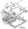
- FIG. 2 and FIG. 3 show the outline structure of the connector 10 that receives the IC card 1 .
- FIG. 4 is a perspective view of the connector 10 as viewed diagonally from behind.
- the connector 10 is secured to an appropriate location on an electronic device, such as a cellular phone, a telephone, a PDA, a portable audio device and a camera.
- the connector 10 has a lower housing 20 and an upper housing (upper cover body) 30 .
- the lower housing 20 is made from an insulating material such as resin.
- the upper housing 30 is made from a worked metal sheet and functions as a cover body covering the lower housing 20 .
- the reason why the upper housing 30 is made from a metal sheet, not resin, is that the metal has a greater strength than the resin and thus can reduce the height of the connector.
- the connector 10 has a card insertion opening 11 at the front through which the card 1 is inserted. Both inner side surfaces of the lower housing 20 are formed with guide rails 12 that guide the card 1 as it is inserted or retracted.
- a base plate of the lower housing 20 is formed with a plurality of grooves 13 in which a plurality of contact terminals 40 made from cantilevered contact leaf springs are positioned and press-fitted under pressure, respectively.
- the contact terminals 40 are used as power supply terminals and signal terminals.
- the contact terminals 40 each have at their front ends a contact portion 40 a projecting in an arc and adapted to contact associated one of the plurality of contact pads formed on the card 1 .
- Terminal portions 40 b of the contact terminals 40 are soldered to contact pads of a printed circuit board of the electronic device.
- a metal contact leaf spring 50 forming one of contacts of a write protect switch SW 1 and a metal contact leaf spring 60 forming one of contacts of a card recognition switch SW 2 are secured to the lower housing 20 by means of a press fit or a pin.
- the metal upper housing 30 has a pair of leaf springs 35 a , 35 b facing the guide rails 12 to firmly hold the inserted card 1 .
- One bent side plate 30 a of the metal upper housing 30 is formed with a metal leaf spring 70 that constitutes the other contact of the write protect switch SW 1 .
- a top plate 30 b of the upper housing 30 has a metal leaf spring 80 formed on the rear end side thereof which constitutes the other contact of the card recognition switch SW 2 .
- the write protect switch SW 1 made up of the contact leaf spring 50 secured to the lower housing 20 and the contact leaf spring 70 formed in the metal upper housing 30 will be explained by referring to FIGS. 5, 6 A and 6 B also.
- the write protect switch SW 1 detects the slide position of the write protect button 3 of the inserted card 1 .
- the contact leaf spring 50 secured to the lower housing 20 is made from a metal piece which comprises a terminal portion 51 secured to the contact pad of a the printed circuit board, a stationary portion 52 secured to the lower housing 20 , a leaf spring portion 53 extending along the card side surface, and a front engagement portion 54 projecting in an arc. With the stationary portion 52 rigidly fixed, the contact leaf spring 50 is supported like a cantilevered beam.
- the front engagement portion 54 as shown in FIGS. 6A and 6B, has an engagement portion 54 a and a front contact portion 54 b at the front end of the engagement portion 54 a .
- the engagement portion 54 a engages with the front part 2 a of the recess 2 formed in the card 1 or the write protect button 3 slid to the front part 2 a when the card 1 is inserted.
- the contact leaf spring 50 has its leaf spring portion 53 urged so that when the card 1 is inserted, the engagement portion 54 a is pressed against the bottom surface of the front part 2 a of the recess 2 of the card 1 .
- the contact leaf spring 70 extending from the side plate 30 a of the metal upper housing 30 is made from a metal piece which has a leaf spring portion 73 and a front engagement portion 74 projecting in an arc.
- the contact leaf spring 70 also has a contact projection 75 in the leaf spring portion 73 that contacts the front contact portion 54 b of the contact leaf spring 50 .
- the front engagement portion 74 engages with the rear part 2 b of the recess 2 of the card 1 or the write protect button 3 slid to the rear part 2 b when the card 1 is inserted.
- the contact leaf spring 70 has its leaf spring portion 73 urged so that when the card 1 is inserted, the front engagement portion 74 is pressed against the bottom surface of the rear part 2 b of the recess 2 of the card 1 .
- the metal upper housing 30 is electrically connected to the ground of the printed circuit board.
- the terminal portion 51 of the contact leaf spring 50 secured to the lower housing 20 is applied an appropriate voltage.
- the engagement portion 54 a of the contact leaf spring 50 engages with the write protect button 3 situated at the front part 2 a of the recess 2 of the card 1 and the front engagement portion 74 of the contact leaf spring 70 engages with the bottom surface of the rear part 2 b of the recess 2 of the card 1 .
- the two contact leaf springs 50 , 70 are in contact with each other through the front contact portion 54 b and the contact projection 75 and the write protection switch SW 1 is on.
- these contact leaf springs 50 , 70 are brought into or out of contact with each other according to the position of the write protect button 3 .
- electrically detecting the engagement or disengagement between the contact leaf springs 50 , 70 can determine at which of the write-disable/write-enable positions the write protect button 3 of the IC card 1 is situated.
- the engagement portion of one contact leaf spring engages with the write protect button 3 and the engagement portion of the other contact leaf spring engages with a part of the recess 2 adjacent to the write protect button.
- the structure of the switch SW 1 can engage or disengage the two contact leaf springs 50 , 70 through their relative displacement equal to two times the height of the write protect button 3 , this switch structure is effectively applied to a small card which cannot keep a sufficient height for the write protect button.
- the card recognition switch SW 2 made up of the contact leaf spring 60 secured to the lower housing 20 and the contact leaf spring 80 formed in the metal upper housing 30 will be described by referring also to FIG. 7 .
- the card recognition switch SW 2 detects whether or not the card 1 is fully inserted into the connector 10 .
- the contact leaf spring 60 secured to the lower housing 20 comprises a terminal portion 61 fixedly connected to the contact pad of the printed circuit board, a grip portion 62 for gripping the top and bottom portions of the lower housing 20 to securely hold the contact leaf spring 60 , a folded leaf spring portion 63 , an engagement portion 64 protruding to engage with the front end face of the inserted card 1 , and a folded contact portion 65 projecting upward from the leaf spring portion 63 .
- the contact leaf spring 80 formed at the rear end portion of the upper housing 30 is made from a metal piece having a leaf spring portion 83 and a front end contact portion 85 .
- the metal upper housing 30 is electrically connected to the ground of the printed circuit board, as described earlier.
- the terminal portion 61 of the contact leaf spring 60 secured to the lower housing 20 is applied an appropriate voltage.
- the metal upper housing 30 as the upper cover of the connector housing is formed with one of paired metal pieces forming the write protect switch SW 1 and with one of paired metal pieces forming the card recognition switch SW 2 , it is possible to reduce the number of parts of the switches and simplify the structure for holding the metal pieces, which in turn lead to reduced cost and space.
- the positional relation may be reversed, i.e., the button position indicated by the solid line in FIG. 1 may correspond to the write-disable position and the position indicated by the dashed line may correspond to the write-enable position.
- the contact leaf spring 60 is of a folded type, it may use the same type of leaf spring as other contact leaf springs 50 , 70 . Further, the leaf springs 50 - 80 may have any other desired shape as long as various states, such as the protect button position and the presence or absence of an inserted card, are detected by utilizing the elastic engagement or disengagement between these leaf springs.
- the above embodiment uses two switches in detecting the protect button position and the presence or absence of an inserted card, if additional switches are necessary to detect other states, one of the paired metal pieces making up each of the additional switches need only be formed in the metal upper housing 30 .
- the metal upper housing as the upper cover of the connector housing is formed with one of the paired contact pieces making up each of one or more switches, it is possible to reduce the number of parts of the switches and simplify the structure for holding the contact pieces, leading to reduced cost and space.
Abstract
One of each pair of metal pieces 70, 80 making up each of the switches SW1, SW2 is formed in the metal upper housing 30 to reduce the number of parts of the switches arranged in the connector and to efficiently arrange these switches in a small space.
Description
The present invention relates to a card connector for connecting an IC card to an electronic device, such as a cellular phone, a telephone, a PDA (personal digital assistant), a portable audio device and a camera etc., and more specifically to a structure of various switches installed in the connector.
In electronic devices such as cellular phones, telephones, PDAs and digital cameras, a variety of functions are added by inserting an IC card with a built-in memory or control ICs, such as a SIM (subscriber identity module), an MMC (multimedia card), a Smart Media (tradename) and an SD (super density or secure digital) card.
In a connector structure for removably accommodating such an IC card, a plurality of contact terminals made from a metal leaf spring are provided in a connector housing to make contact with a plurality of contact pads formed on the front or back surface of the inserted IC card to electrically connect the IC card to the electronic device mounting that connector. The contact pads of the IC card include a power supply pad connected to a power supply line and a plurality of signal pads for transferring various signals. These contact pads are connected via the contact terminals of the card connector to a power supply circuit and various signal processing circuits in the electronic device.
The IC card of this kind normally employs some means for prohibiting writing operations in order to protect information stored in its internal memory. One such means is a write protect button that can slide between two positions, as in a floppy disk. In such a slide button system, the card is provided with a write protect button that can slide between two positions and which, when it is situated at one position, sets the card to a write-disable state and, when it is slid to the other position, sets it to a write-enable state. On the connector side, a detector needs to be provided that detects the slide positions of the write protect button.
Further, in addition to the slide position signal of the write protect button, the electronic device often calls for a signal indicating whether the card is inserted or not. Hence, the connector should also be provided with a detector for checking the card insertion.
As a sensor structure for detecting a variety of these states, a light-based sensor structure may be conceived. The light-based sensor structure, however, has drawbacks that a sufficient detection precision cannot be expected as the card becomes thinner and smaller and that the installation of a light sensor can be a hindrance to reductions in size and cost. Hence, a sensor structure utilizing engagement and disengagement of a contact leaf spring is considered the most promising structure overall.
When these detectors are to be constructed of contact leaf springs, because each detector requires a pair of contact leaf springs, the total number of contact leaf springs and contact leaf spring support structures required in the connector as a whole is two times the number of detectors.
Such a construction therefore has a large number of parts making up the detectors and requires a large space to accommodate these parts, which is detrimental to reducing the weight, thickness and size of the connector structure.
The present invention has been accomplished under these circumstances. It is an object of the present invention to solve the above-described problems by providing a card connector which can construct one or more switches in the connector with a reduced number of parts and accommodate these switches in a smaller space efficiently.
According to one aspect of the present invention, a card connector is provided, which comprises: a connector housing having a lower housing and a metal upper housing; contact terminals arranged to engage external contacts of a card inserted into the connector housing; and one or more switches each operated by an engagement and disengagement of a pair of metal pieces; wherein one of the each pair of metal pieces making up each of the switches is formed in the metal upper housing.
In this invention, one of each pair of metal pieces making up each of the switches is formed in the metal cover body made from a worked metal sheet. This construction can reduce the number of parts of the switches and also the space of the connector.
FIG. 1 is a plan view showing an example of an IC card for insertion into a card connector of this invention.
FIG. 2 is an exploded perspective view showing an outline construction of one embodiment of the card connector according to the invention.
FIG. 3 is an exploded perspective view showing an outline construction of the embodiment of the card connector according to the invention.
FIG. 4 is an exploded perspective view showing an outline construction of the embodiment of the card connector according to the invention.
FIG. 5 is an enlarged perspective view showing an embodiment of a switch structure on a write protect switch side.
FIG. 6A and FIG. 6B are schematic diagrams showing the operation of the write protect switch.
FIG. 7 is an enlarged perspective view showing an embodiment of a switch structure on a card recognition switch side.
Now, embodiments of the present invention will be described in detail with reference to the accompanying drawings.
FIG. 1 is a plan view showing an example of an IC card to be inserted into the card connector of this invention.
The IC card 1 has a recess 2 formed in its side surface in which a write protect button 3 can be slid in the card insertion/retraction direction (direction of arrow A). In this case, the write protect button 3 can assume either of two positions, a protect-off (write-enable) position indicated by a solid line and a protect-on (write-disable) position indicated by a dashed line, and can be slid between these two positions. That is, the card 1 is write-enabled when the write protect button 3 is set to a rear part 2 b of the recess 2 and write-disabled when the bottom 3 is set to a front part 2 a of the recess 2. Though not shown in FIG. 1, the back surface of the card 1 is formed with a plurality of contact pads, including power supply pads and signal pads, which come into contact with the contact terminals on the connector side.
FIG. 2 and FIG. 3 show the outline structure of the connector 10 that receives the IC card 1. FIG. 4 is a perspective view of the connector 10 as viewed diagonally from behind. The connector 10 is secured to an appropriate location on an electronic device, such as a cellular phone, a telephone, a PDA, a portable audio device and a camera.
In FIG. 2 to FIG. 4, the connector 10 has a lower housing 20 and an upper housing (upper cover body) 30. The lower housing 20 is made from an insulating material such as resin. The upper housing 30 is made from a worked metal sheet and functions as a cover body covering the lower housing 20. The reason why the upper housing 30 is made from a metal sheet, not resin, is that the metal has a greater strength than the resin and thus can reduce the height of the connector.
The connector 10 has a card insertion opening 11 at the front through which the card 1 is inserted. Both inner side surfaces of the lower housing 20 are formed with guide rails 12 that guide the card 1 as it is inserted or retracted.
A base plate of the lower housing 20 is formed with a plurality of grooves 13 in which a plurality of contact terminals 40 made from cantilevered contact leaf springs are positioned and press-fitted under pressure, respectively. The contact terminals 40 are used as power supply terminals and signal terminals. The contact terminals 40 each have at their front ends a contact portion 40 a projecting in an arc and adapted to contact associated one of the plurality of contact pads formed on the card 1. Terminal portions 40 b of the contact terminals 40 are soldered to contact pads of a printed circuit board of the electronic device.
A metal contact leaf spring 50 forming one of contacts of a write protect switch SW1 and a metal contact leaf spring 60 forming one of contacts of a card recognition switch SW2 are secured to the lower housing 20 by means of a press fit or a pin.
The metal upper housing 30 has a pair of leaf springs 35 a, 35 b facing the guide rails 12 to firmly hold the inserted card 1.
One bent side plate 30 a of the metal upper housing 30 is formed with a metal leaf spring 70 that constitutes the other contact of the write protect switch SW1.
On the other hand, a top plate 30 b of the upper housing 30 has a metal leaf spring 80 formed on the rear end side thereof which constitutes the other contact of the card recognition switch SW2.
First, the write protect switch SW1 made up of the contact leaf spring 50 secured to the lower housing 20 and the contact leaf spring 70 formed in the metal upper housing 30 will be explained by referring to FIGS. 5, 6A and 6B also. The write protect switch SW1 detects the slide position of the write protect button 3 of the inserted card 1.
The contact leaf spring 50 secured to the lower housing 20 is made from a metal piece which comprises a terminal portion 51 secured to the contact pad of a the printed circuit board, a stationary portion 52 secured to the lower housing 20, a leaf spring portion 53 extending along the card side surface, and a front engagement portion 54 projecting in an arc. With the stationary portion 52 rigidly fixed, the contact leaf spring 50 is supported like a cantilevered beam. The front engagement portion 54, as shown in FIGS. 6A and 6B, has an engagement portion 54 a and a front contact portion 54 b at the front end of the engagement portion 54 a. The engagement portion 54 a engages with the front part 2 a of the recess 2 formed in the card 1 or the write protect button 3 slid to the front part 2 a when the card 1 is inserted. The contact leaf spring 50 has its leaf spring portion 53 urged so that when the card 1 is inserted, the engagement portion 54 a is pressed against the bottom surface of the front part 2 a of the recess 2 of the card 1.
The contact leaf spring 70 extending from the side plate 30 a of the metal upper housing 30 is made from a metal piece which has a leaf spring portion 73 and a front engagement portion 74 projecting in an arc. The contact leaf spring 70 also has a contact projection 75 in the leaf spring portion 73 that contacts the front contact portion 54 b of the contact leaf spring 50. As shown in FIG. 6A and FIG. 6B, the front engagement portion 74 engages with the rear part 2 b of the recess 2 of the card 1 or the write protect button 3 slid to the rear part 2 b when the card 1 is inserted. The contact leaf spring 70 has its leaf spring portion 73 urged so that when the card 1 is inserted, the front engagement portion 74 is pressed against the bottom surface of the rear part 2 b of the recess 2 of the card 1.
In the switch SW1 described above, the metal upper housing 30 is electrically connected to the ground of the printed circuit board. The terminal portion 51 of the contact leaf spring 50 secured to the lower housing 20 is applied an appropriate voltage.
In this switch SW1, when the write protect button 3 of the inserted card 1 is set at the write-enable position, as shown in FIG. 6A, the engagement portion 54 a of the contact leaf spring 50 engages with the bottom surface of the front part 2 a of the recess 2 of the card 1 and the front engagement portion 74 of the contact leaf spring 70 engages with the write protect button 3 of the card 1. At this time, the two contact leaf springs 50, 70 are separated from each other in any part and the write protect switch SW1 is off.
When on the other hand the write protection button 3 is set at the write-disable position, as shown in FIG. 6B, the engagement portion 54 a of the contact leaf spring 50 engages with the write protect button 3 situated at the front part 2 a of the recess 2 of the card 1 and the front engagement portion 74 of the contact leaf spring 70 engages with the bottom surface of the rear part 2 b of the recess 2 of the card 1. At this time, the two contact leaf springs 50, 70 are in contact with each other through the front contact portion 54 b and the contact projection 75 and the write protection switch SW1 is on.
In the write protect switch SW1 made up of the two contact leaf springs 50, 70, these contact leaf springs 50, 70 are brought into or out of contact with each other according to the position of the write protect button 3. Thus, electrically detecting the engagement or disengagement between the contact leaf springs 50, 70 can determine at which of the write-disable/write-enable positions the write protect button 3 of the IC card 1 is situated.
In this structure of the switch SW1, at whichever of the two slide positions the write protect button 3 is situated, the engagement portion of one contact leaf spring engages with the write protect button 3 and the engagement portion of the other contact leaf spring engages with a part of the recess 2 adjacent to the write protect button. Hence, if there is a play due to differences between the width of the card accommodating portion of the connector 10 and the width of the card 1, or parts tolerances or assembly tolerances, the shift in the position of the write protect button 3 can always cause the contact leaf springs 50, 70 to be displaced by a distance equal to the height of the write protect button 3.
In this structure of the switch SW1, because the write protect button 3 and the part of the recess 2 adjacent to the bottom 3 are used to bring the contact leaf springs 50, 70 into or out of contact with each other, the directions of displacements of the contact leaf springs 50, 70 are opposite. For example, when the state changes from the one shown in FIG. 6A where the contact leaf springs 50, 70 are separated to the one shown in FIG. 6B where the contact leaf springs 50, 70 abut each other, the contact leaf springs 50, 70 move toward each other until they engage. The shift from the state of FIG. 6B to the state of FIG. 6A is reverse to the process above and the contact leaf springs 50, 70 move away from each other until they are parted.
As described above, because the structure of the switch SW1 can engage or disengage the two contact leaf springs 50, 70 through their relative displacement equal to two times the height of the write protect button 3, this switch structure is effectively applied to a small card which cannot keep a sufficient height for the write protect button.
Next, the card recognition switch SW2 made up of the contact leaf spring 60 secured to the lower housing 20 and the contact leaf spring 80 formed in the metal upper housing 30 will be described by referring also to FIG. 7. The card recognition switch SW2 detects whether or not the card 1 is fully inserted into the connector 10.
The contact leaf spring 60 secured to the lower housing 20 comprises a terminal portion 61 fixedly connected to the contact pad of the printed circuit board, a grip portion 62 for gripping the top and bottom portions of the lower housing 20 to securely hold the contact leaf spring 60, a folded leaf spring portion 63, an engagement portion 64 protruding to engage with the front end face of the inserted card 1, and a folded contact portion 65 projecting upward from the leaf spring portion 63.
On the other hand, the contact leaf spring 80 formed at the rear end portion of the upper housing 30 is made from a metal piece having a leaf spring portion 83 and a front end contact portion 85.
In this switch SW2, the metal upper housing 30 is electrically connected to the ground of the printed circuit board, as described earlier. The terminal portion 61 of the contact leaf spring 60 secured to the lower housing 20 is applied an appropriate voltage.
In this card recognition switch SW2 made up of these two contact leaf springs 60, 80, when the card 1 is not inserted, the contact leaf springs 60, 80 have their contact portions 65, 85 separated, leaving the card recognition switch SW2 turned off.
When the card 1 is fully inserted into the connector 10, the engagement portion 64 of the contact leaf spring 60 is pushed by the front end face of the card 1, displacing the contact portion 65 rearwardly. As a result, the contact portion 65 of the contact leaf spring 60 and the front end contact portion 85 of the contact leaf spring 80 engage with each other, turning on the card recognition switch SW2.
In this embodiment, because the metal upper housing 30 as the upper cover of the connector housing is formed with one of paired metal pieces forming the write protect switch SW1 and with one of paired metal pieces forming the card recognition switch SW2, it is possible to reduce the number of parts of the switches and simplify the structure for holding the metal pieces, which in turn lead to reduced cost and space.
In the above embodiment, while the button position indicated by a solid line in FIG. 1 corresponds to the write-enable position and the position indicated by a dashed line corresponds to the write-disable position, the positional relation may be reversed, i.e., the button position indicated by the solid line in FIG. 1 may correspond to the write-disable position and the position indicated by the dashed line may correspond to the write-enable position.
In the above embodiment, although the contact leaf spring 60 is of a folded type, it may use the same type of leaf spring as other contact leaf springs 50, 70. Further, the leaf springs 50-80 may have any other desired shape as long as various states, such as the protect button position and the presence or absence of an inserted card, are detected by utilizing the elastic engagement or disengagement between these leaf springs.
Although the above embodiment uses two switches in detecting the protect button position and the presence or absence of an inserted card, if additional switches are necessary to detect other states, one of the paired metal pieces making up each of the additional switches need only be formed in the metal upper housing 30.
As described above, because in this invention the metal upper housing as the upper cover of the connector housing is formed with one of the paired contact pieces making up each of one or more switches, it is possible to reduce the number of parts of the switches and simplify the structure for holding the contact pieces, leading to reduced cost and space.
Claims (5)
1. A card connector comprising:
a connector housing having a lower housing and a metal upper housing;
contact terminals arranged on the connector housing to engage with contact pads of an inserted card; and
one or more switches each operated by engagement and disengagement of a pair of metal pieces;
wherein at least one of said one or more switches comprises:
a first contact leaf spring formed on said connector housing, said first contact leaf spring having an engagement portion for engaging with a button of said inserted card when the button is in a first position;
a second contact leaf spring having an engagement portion for engaging with said button of said inserted card when the button is in a second position; and
a contact portion provided on at least one of said first contact leaf spring and said second contact leaf spring for electrically connecting said first contact leaf spring to said second contact leaf spring when said button of said inserted card is located in one of the first position and the second position.
2. A card connector according to claim 1 , wherein each of said first contact leaf spring and said second contact leaf spring is a contact leaf spring extending from an end portion of said connector housing like a cantilevered beam.
3. A card connector according to claim 1 , wherein when one of said one or more switches is a card recognition switch to detect the presence or absence of the inserted card, one metal piece of said pair of metal pieces making up said card recognition switch is formed as a portion of said metal upper housing.
4. A card connector according to claim 1 , wherein said inserted card has a slidable write protect button at a side surface thereof and said first contact leaf spring and said second contact leaf spring each are a write protect switch configured to detect a slide position of the write protect button of said inserted card.
5. A card connector according to claim 1 or 2 , wherein one of said first contact leaf spring and said second contact leaf spring is formed as a portion of said metal upper housing.
Applications Claiming Priority (3)
| Application Number | Priority Date | Filing Date | Title |
|---|---|---|---|
| JP31750899A JP3377477B2 (en) | 1999-11-08 | 1999-11-08 | Card connector |
| JP11-317508 | 1999-11-08 | ||
| PCT/JP2000/007761 WO2001035332A1 (en) | 1999-11-08 | 2000-11-02 | Card connector |
Publications (1)
| Publication Number | Publication Date |
|---|---|
| US6692276B1 true US6692276B1 (en) | 2004-02-17 |
Family
ID=18089029
Family Applications (1)
| Application Number | Title | Priority Date | Filing Date |
|---|---|---|---|
| US09/889,007 Expired - Fee Related US6692276B1 (en) | 1999-11-08 | 2000-11-02 | Card connector |
Country Status (5)
| Country | Link |
|---|---|
| US (1) | US6692276B1 (en) |
| EP (1) | EP1146473B1 (en) |
| JP (1) | JP3377477B2 (en) |
| DE (1) | DE60037721T2 (en) |
| WO (1) | WO2001035332A1 (en) |
Cited By (13)
| Publication number | Priority date | Publication date | Assignee | Title |
|---|---|---|---|---|
| US6749450B1 (en) * | 2003-04-03 | 2004-06-15 | Egbon Electronics Ltd. | Socket for a memory card |
| US6786761B1 (en) * | 2003-04-28 | 2004-09-07 | Hewlett-Packard Development Company, L.P. | Method and system for sensing the status of a ZIF socket lever |
| US20050059281A1 (en) * | 2001-03-09 | 2005-03-17 | Bricaud Herve Guy | Connector for high capacity smart |
| US20050254219A1 (en) * | 1999-08-24 | 2005-11-17 | Seiji Nakanishi | Memory card |
| US20060076409A1 (en) * | 2004-10-13 | 2006-04-13 | Sheng-Ching Ko | Card reading apparatus |
| US20060089052A1 (en) * | 2004-10-27 | 2006-04-27 | Hon Hai Precision Ind. Co., Ltd. | Card connector with detect switch |
| US20060121759A1 (en) * | 2003-06-16 | 2006-06-08 | Arkray Inc. | Connector |
| US20080009163A1 (en) * | 2005-04-21 | 2008-01-10 | Japan Aviation Electronics Industry, Limited | Card Connector |
| US20080254657A1 (en) * | 2007-04-11 | 2008-10-16 | Hon Hai Precision Ind. Co., Ltd. | Electrical card connector |
| US20100120281A1 (en) * | 2008-11-07 | 2010-05-13 | Tai-Sol Electronics Co., Ltd. | Card connector capable of detecting card insertion |
| US20100297886A1 (en) * | 2009-05-19 | 2010-11-25 | Tai-Sol Electronics Co., Ltd. | Card connector capable of detecting card entry |
| US20110104920A1 (en) * | 2008-05-30 | 2011-05-05 | Japan Aviation Electronics Industry, Limited | Card socket |
| US20140004735A1 (en) * | 2012-07-02 | 2014-01-02 | Tyco Electronics Japan G.K. | Card Connector |
Families Citing this family (7)
| Publication number | Priority date | Publication date | Assignee | Title |
|---|---|---|---|---|
| US7295443B2 (en) | 2000-07-06 | 2007-11-13 | Onspec Electronic, Inc. | Smartconnect universal flash media card adapters |
| US6438638B1 (en) | 2000-07-06 | 2002-08-20 | Onspec Electronic, Inc. | Flashtoaster for reading several types of flash-memory cards with or without a PC |
| JP4646449B2 (en) * | 2001-06-29 | 2011-03-09 | モレックス インコーポレイテド | Card connector |
| US7210950B2 (en) | 2003-05-26 | 2007-05-01 | Matsushita Electric Works, Ltd. | Connector for memory card |
| JP4023389B2 (en) * | 2003-05-26 | 2007-12-19 | 松下電工株式会社 | Memory card socket |
| JP5329792B2 (en) * | 2007-10-29 | 2013-10-30 | 富士通コンポーネント株式会社 | Card connector |
| JP4669537B2 (en) * | 2008-08-25 | 2011-04-13 | アルプス電気株式会社 | Card connector |
Citations (22)
| Publication number | Priority date | Publication date | Assignee | Title |
|---|---|---|---|---|
| US3283107A (en) | 1964-07-20 | 1966-11-01 | Sangamo Electric Co | Interrupter having positive stop means for contact elements |
| EP0284431A2 (en) | 1987-03-27 | 1988-09-28 | Mitsubishi Denki Kabushiki Kaisha | Mechanism for connecting IC card and external device |
| JPH0596941A (en) | 1991-10-08 | 1993-04-20 | Nippondenso Co Ltd | Vehicle humidifying device |
| EP0669590A2 (en) | 1994-02-23 | 1995-08-30 | Molex Incorporated | IC pack connector with detect switch |
| JPH08166906A (en) | 1994-12-13 | 1996-06-25 | Hitachi Maxell Ltd | Semiconductor device |
| JPH10144422A (en) | 1996-11-08 | 1998-05-29 | Japan Aviation Electron Ind Ltd | Card connector |
| JPH10187896A (en) | 1996-12-24 | 1998-07-21 | Smk Corp | Connector for ic card |
| JPH10255012A (en) | 1997-02-28 | 1998-09-25 | Amphenol Tuchel Electron Gmbh | Chip cad reader |
| JPH10255910A (en) | 1997-03-14 | 1998-09-25 | Mitsumi Electric Co Ltd | Ic card connector |
| US5820391A (en) | 1996-07-02 | 1998-10-13 | Thomas & Betts International, Inc. | Miniature card interface connector |
| EP0908981A2 (en) | 1997-09-16 | 1999-04-14 | Alps Electric Co., Ltd. | IC card connector |
| JPH11149956A (en) | 1997-11-17 | 1999-06-02 | Hosiden Corp | Card connector |
| US5911587A (en) * | 1997-02-26 | 1999-06-15 | The Whitaker Corporation | Card reader having a configurable switch |
| US6004155A (en) | 1998-07-28 | 1999-12-21 | Hon Hai Precision Ind. Co., Ltd. | Card connector |
| US6015311A (en) * | 1996-12-17 | 2000-01-18 | The Whitaker Corporation | Contact configuration for smart card reader |
| US6039599A (en) | 1997-06-30 | 2000-03-21 | The Whitaker Corporation | Switch for a card reader assembly |
| US6073853A (en) | 1997-05-30 | 2000-06-13 | Framatome Connectors International | Connector for a card reader having contacts with twofold detection |
| US6099335A (en) * | 1999-04-30 | 2000-08-08 | Hon Hai Precision Ind. Co., Ltd. | Electrical card connector |
| US6126464A (en) | 1998-06-06 | 2000-10-03 | Hon Hai Precision Ind. Co., Ltd. | Card connector having switching means |
| US6129571A (en) | 1998-11-27 | 2000-10-10 | Kel Corporation | IC card connector |
| WO2001035331A1 (en) | 1999-11-05 | 2001-05-17 | Yamaichi Electronics Co., Ltd. | Switching construction for card connectors |
| US6399906B1 (en) | 1999-11-05 | 2002-06-04 | Yamaichi Electronics Co., Ltd. | Switch for a card connector |
Family Cites Families (6)
| Publication number | Priority date | Publication date | Assignee | Title |
|---|---|---|---|---|
| JPH06139414A (en) * | 1992-10-28 | 1994-05-20 | Sony Corp | Ic card detecting device |
| DE19521721B4 (en) * | 1995-06-14 | 2006-12-07 | Amphenol-Tuchel Electronics Gmbh | Shielded contacting device |
| JPH09147068A (en) * | 1995-11-17 | 1997-06-06 | Toshiba Corp | Ic card reader/writer |
| US6062889A (en) * | 1997-01-13 | 2000-05-16 | The Whitaker Corporation | Module connector having a switching mechanism |
| US6326568B2 (en) * | 1997-07-02 | 2001-12-04 | Molex Incorporated | Blade switch assembly for a card reader |
| JPH11297415A (en) * | 1998-04-03 | 1999-10-29 | Molex Inc | Connector for card |
-
1999
- 1999-11-08 JP JP31750899A patent/JP3377477B2/en not_active Expired - Fee Related
-
2000
- 2000-11-02 EP EP00971780A patent/EP1146473B1/en not_active Expired - Lifetime
- 2000-11-02 US US09/889,007 patent/US6692276B1/en not_active Expired - Fee Related
- 2000-11-02 DE DE60037721T patent/DE60037721T2/en not_active Expired - Fee Related
- 2000-11-02 WO PCT/JP2000/007761 patent/WO2001035332A1/en active IP Right Grant
Patent Citations (23)
| Publication number | Priority date | Publication date | Assignee | Title |
|---|---|---|---|---|
| US3283107A (en) | 1964-07-20 | 1966-11-01 | Sangamo Electric Co | Interrupter having positive stop means for contact elements |
| EP0284431A2 (en) | 1987-03-27 | 1988-09-28 | Mitsubishi Denki Kabushiki Kaisha | Mechanism for connecting IC card and external device |
| JPH0596941A (en) | 1991-10-08 | 1993-04-20 | Nippondenso Co Ltd | Vehicle humidifying device |
| EP0669590A2 (en) | 1994-02-23 | 1995-08-30 | Molex Incorporated | IC pack connector with detect switch |
| JPH08166906A (en) | 1994-12-13 | 1996-06-25 | Hitachi Maxell Ltd | Semiconductor device |
| US5820391A (en) | 1996-07-02 | 1998-10-13 | Thomas & Betts International, Inc. | Miniature card interface connector |
| JPH10144422A (en) | 1996-11-08 | 1998-05-29 | Japan Aviation Electron Ind Ltd | Card connector |
| US6015311A (en) * | 1996-12-17 | 2000-01-18 | The Whitaker Corporation | Contact configuration for smart card reader |
| JPH10187896A (en) | 1996-12-24 | 1998-07-21 | Smk Corp | Connector for ic card |
| US5911587A (en) * | 1997-02-26 | 1999-06-15 | The Whitaker Corporation | Card reader having a configurable switch |
| JPH10255012A (en) | 1997-02-28 | 1998-09-25 | Amphenol Tuchel Electron Gmbh | Chip cad reader |
| JPH10255910A (en) | 1997-03-14 | 1998-09-25 | Mitsumi Electric Co Ltd | Ic card connector |
| US6073853A (en) | 1997-05-30 | 2000-06-13 | Framatome Connectors International | Connector for a card reader having contacts with twofold detection |
| US6039599A (en) | 1997-06-30 | 2000-03-21 | The Whitaker Corporation | Switch for a card reader assembly |
| US6059592A (en) | 1997-09-16 | 2000-05-09 | Alps Electric Co., Ltd. | IC card connector having detecting switch for detecting correct installation of IC card |
| EP0908981A2 (en) | 1997-09-16 | 1999-04-14 | Alps Electric Co., Ltd. | IC card connector |
| JPH11149956A (en) | 1997-11-17 | 1999-06-02 | Hosiden Corp | Card connector |
| US6126464A (en) | 1998-06-06 | 2000-10-03 | Hon Hai Precision Ind. Co., Ltd. | Card connector having switching means |
| US6004155A (en) | 1998-07-28 | 1999-12-21 | Hon Hai Precision Ind. Co., Ltd. | Card connector |
| US6129571A (en) | 1998-11-27 | 2000-10-10 | Kel Corporation | IC card connector |
| US6099335A (en) * | 1999-04-30 | 2000-08-08 | Hon Hai Precision Ind. Co., Ltd. | Electrical card connector |
| WO2001035331A1 (en) | 1999-11-05 | 2001-05-17 | Yamaichi Electronics Co., Ltd. | Switching construction for card connectors |
| US6399906B1 (en) | 1999-11-05 | 2002-06-04 | Yamaichi Electronics Co., Ltd. | Switch for a card connector |
Cited By (23)
| Publication number | Priority date | Publication date | Assignee | Title |
|---|---|---|---|---|
| US7324347B2 (en) * | 1999-08-24 | 2008-01-29 | Matsushita Electric Industrial Co., Ltd. | Memory card |
| US20050254219A1 (en) * | 1999-08-24 | 2005-11-17 | Seiji Nakanishi | Memory card |
| US20050059281A1 (en) * | 2001-03-09 | 2005-03-17 | Bricaud Herve Guy | Connector for high capacity smart |
| US7033221B2 (en) * | 2001-03-09 | 2006-04-25 | Itt Manufacturing Enterprise, Inc. | Connector for high capacity smart cards |
| US6749450B1 (en) * | 2003-04-03 | 2004-06-15 | Egbon Electronics Ltd. | Socket for a memory card |
| US6786761B1 (en) * | 2003-04-28 | 2004-09-07 | Hewlett-Packard Development Company, L.P. | Method and system for sensing the status of a ZIF socket lever |
| US20060121759A1 (en) * | 2003-06-16 | 2006-06-08 | Arkray Inc. | Connector |
| US7183508B2 (en) * | 2003-06-16 | 2007-02-27 | Arkray Inc. | Connector |
| US20060076409A1 (en) * | 2004-10-13 | 2006-04-13 | Sheng-Ching Ko | Card reading apparatus |
| US20060089052A1 (en) * | 2004-10-27 | 2006-04-27 | Hon Hai Precision Ind. Co., Ltd. | Card connector with detect switch |
| US7137836B2 (en) * | 2004-10-27 | 2006-11-21 | Hon Hai Precision Ind. Co., Ltd. | Card connector with detect switch |
| US20080009163A1 (en) * | 2005-04-21 | 2008-01-10 | Japan Aviation Electronics Industry, Limited | Card Connector |
| US7407399B2 (en) | 2005-04-21 | 2008-08-05 | Japan Aviation Electronics Industry, Limited | Card connector |
| US20080254657A1 (en) * | 2007-04-11 | 2008-10-16 | Hon Hai Precision Ind. Co., Ltd. | Electrical card connector |
| US7780476B2 (en) | 2007-04-11 | 2010-08-24 | Hon Hai Precision Ind. Co., Ltd. | Electrical card connector |
| US20110104920A1 (en) * | 2008-05-30 | 2011-05-05 | Japan Aviation Electronics Industry, Limited | Card socket |
| US8523614B2 (en) | 2008-05-30 | 2013-09-03 | Japan Aviation Electronics Industry, Limited | Card socket |
| US20100120281A1 (en) * | 2008-11-07 | 2010-05-13 | Tai-Sol Electronics Co., Ltd. | Card connector capable of detecting card insertion |
| US20100297886A1 (en) * | 2009-05-19 | 2010-11-25 | Tai-Sol Electronics Co., Ltd. | Card connector capable of detecting card entry |
| US20140004735A1 (en) * | 2012-07-02 | 2014-01-02 | Tyco Electronics Japan G.K. | Card Connector |
| CN103531970A (en) * | 2012-07-02 | 2014-01-22 | 泰科电子日本合同会社 | Card connector |
| US9039440B2 (en) * | 2012-07-02 | 2015-05-26 | Tyco Electronics Japan G.K. | Card connector |
| CN103531970B (en) * | 2012-07-02 | 2018-02-23 | 泰科电子日本合同会社 | Card connector |
Also Published As
| Publication number | Publication date |
|---|---|
| DE60037721D1 (en) | 2008-02-21 |
| JP2001135424A (en) | 2001-05-18 |
| DE60037721T2 (en) | 2008-12-24 |
| EP1146473A1 (en) | 2001-10-17 |
| JP3377477B2 (en) | 2003-02-17 |
| WO2001035332A1 (en) | 2001-05-17 |
| EP1146473A4 (en) | 2004-04-07 |
| EP1146473B1 (en) | 2008-01-09 |
Similar Documents
| Publication | Publication Date | Title |
|---|---|---|
| US6692276B1 (en) | Card connector | |
| US6638087B1 (en) | Switch structure of card connector | |
| US6399906B1 (en) | Switch for a card connector | |
| US6709281B2 (en) | Write protect switch for card connector | |
| US6503092B1 (en) | Card connector | |
| US6402529B2 (en) | Card connector | |
| JP3333481B2 (en) | Card recognition switch for card connector | |
| US6699061B2 (en) | Card connector | |
| US20010039129A1 (en) | Card connector | |
| US7438598B1 (en) | Card connector | |
| EP1406204B1 (en) | Card holder for cellular phone | |
| JP2007294457A (en) | Card connector | |
| US20020102883A1 (en) | Card connector and elastic contact piece | |
| JP3640343B2 (en) | Card connector | |
| JP3507381B2 (en) | Card connector | |
| CN219068576U (en) | Connecting device and electronic equipment | |
| US20060076409A1 (en) | Card reading apparatus |
Legal Events
| Date | Code | Title | Description |
|---|---|---|---|
| AS | Assignment |
Owner name: YAMAICHI ELECTRONICS CO., LTD., JAPAN Free format text: ASSIGNMENT OF ASSIGNORS INTEREST;ASSIGNORS:ABE, KIYOSHI;MATSUDA, EIJI;REEL/FRAME:012290/0218 Effective date: 20010925 |
|
| FEPP | Fee payment procedure |
Free format text: PAYOR NUMBER ASSIGNED (ORIGINAL EVENT CODE: ASPN); ENTITY STATUS OF PATENT OWNER: LARGE ENTITY |
|
| REMI | Maintenance fee reminder mailed | ||
| LAPS | Lapse for failure to pay maintenance fees | ||
| STCH | Information on status: patent discontinuation |
Free format text: PATENT EXPIRED DUE TO NONPAYMENT OF MAINTENANCE FEES UNDER 37 CFR 1.362 |
|
| FP | Lapsed due to failure to pay maintenance fee |
Effective date: 20080217 |