US6708400B2 - Method of attaching printed circuits boards within an electronic module housing - Google Patents
Method of attaching printed circuits boards within an electronic module housing Download PDFInfo
- Publication number
- US6708400B2 US6708400B2 US09/978,341 US97834101A US6708400B2 US 6708400 B2 US6708400 B2 US 6708400B2 US 97834101 A US97834101 A US 97834101A US 6708400 B2 US6708400 B2 US 6708400B2
- Authority
- US
- United States
- Prior art keywords
- circuit board
- particulate
- housing
- electronic module
- layer
- Prior art date
- Legal status (The legal status is an assumption and is not a legal conclusion. Google has not performed a legal analysis and makes no representation as to the accuracy of the status listed.)
- Expired - Fee Related, expires
Links
- 238000000034 method Methods 0.000 title claims description 44
- 229910052751 metal Inorganic materials 0.000 claims abstract description 61
- 239000002184 metal Substances 0.000 claims abstract description 61
- 229910000679 solder Inorganic materials 0.000 claims abstract description 38
- 238000005476 soldering Methods 0.000 claims abstract description 21
- 238000003825 pressing Methods 0.000 claims abstract description 9
- 239000000463 material Substances 0.000 claims description 20
- 239000006261 foam material Substances 0.000 claims description 18
- 239000011521 glass Substances 0.000 claims description 18
- 238000010438 heat treatment Methods 0.000 claims description 12
- 239000002245 particle Substances 0.000 claims description 10
- 230000005496 eutectics Effects 0.000 claims description 4
- 239000005388 borosilicate glass Substances 0.000 claims description 3
- 229920002379 silicone rubber Polymers 0.000 claims description 2
- 238000000151 deposition Methods 0.000 claims 4
- 230000000284 resting effect Effects 0.000 claims 3
- 239000011324 bead Substances 0.000 abstract description 29
- 239000006260 foam Substances 0.000 abstract description 14
- 230000008569 process Effects 0.000 description 18
- 238000004519 manufacturing process Methods 0.000 description 12
- 229910052782 aluminium Inorganic materials 0.000 description 3
- XAGFODPZIPBFFR-UHFFFAOYSA-N aluminium Chemical compound [Al] XAGFODPZIPBFFR-UHFFFAOYSA-N 0.000 description 3
- 230000008901 benefit Effects 0.000 description 2
- 230000005540 biological transmission Effects 0.000 description 2
- QXJJQWWVWRCVQT-UHFFFAOYSA-K calcium;sodium;phosphate Chemical compound [Na+].[Ca+2].[O-]P([O-])([O-])=O QXJJQWWVWRCVQT-UHFFFAOYSA-K 0.000 description 2
- 238000004891 communication Methods 0.000 description 2
- 238000010276 construction Methods 0.000 description 2
- 238000013461 design Methods 0.000 description 2
- 238000012545 processing Methods 0.000 description 2
- 230000001902 propagating effect Effects 0.000 description 2
- 239000002470 thermal conductor Substances 0.000 description 2
- RTAQQCXQSZGOHL-UHFFFAOYSA-N Titanium Chemical compound [Ti] RTAQQCXQSZGOHL-UHFFFAOYSA-N 0.000 description 1
- 230000009471 action Effects 0.000 description 1
- 230000002411 adverse Effects 0.000 description 1
- 230000001680 brushing effect Effects 0.000 description 1
- 230000008859 change Effects 0.000 description 1
- 238000004140 cleaning Methods 0.000 description 1
- 239000011248 coating agent Substances 0.000 description 1
- 238000000576 coating method Methods 0.000 description 1
- 238000010586 diagram Methods 0.000 description 1
- 230000000694 effects Effects 0.000 description 1
- 230000013011 mating Effects 0.000 description 1
- 239000000155 melt Substances 0.000 description 1
- 238000012986 modification Methods 0.000 description 1
- 230000004048 modification Effects 0.000 description 1
- 239000000615 nonconductor Substances 0.000 description 1
- 230000010355 oscillation Effects 0.000 description 1
- 230000000644 propagated effect Effects 0.000 description 1
- 239000002904 solvent Substances 0.000 description 1
- 239000010936 titanium Substances 0.000 description 1
- 229910052719 titanium Inorganic materials 0.000 description 1
Images


Classifications
-
- H—ELECTRICITY
- H05—ELECTRIC TECHNIQUES NOT OTHERWISE PROVIDED FOR
- H05K—PRINTED CIRCUITS; CASINGS OR CONSTRUCTIONAL DETAILS OF ELECTRIC APPARATUS; MANUFACTURE OF ASSEMBLAGES OF ELECTRICAL COMPONENTS
- H05K3/00—Apparatus or processes for manufacturing printed circuits
- H05K3/0058—Laminating printed circuit boards onto other substrates, e.g. metallic substrates
- H05K3/0061—Laminating printed circuit boards onto other substrates, e.g. metallic substrates onto a metallic substrate, e.g. a heat sink
-
- H—ELECTRICITY
- H05—ELECTRIC TECHNIQUES NOT OTHERWISE PROVIDED FOR
- H05K—PRINTED CIRCUITS; CASINGS OR CONSTRUCTIONAL DETAILS OF ELECTRIC APPARATUS; MANUFACTURE OF ASSEMBLAGES OF ELECTRICAL COMPONENTS
- H05K1/00—Printed circuits
- H05K1/02—Details
- H05K1/0213—Electrical arrangements not otherwise provided for
- H05K1/0237—High frequency adaptations
-
- H—ELECTRICITY
- H05—ELECTRIC TECHNIQUES NOT OTHERWISE PROVIDED FOR
- H05K—PRINTED CIRCUITS; CASINGS OR CONSTRUCTIONAL DETAILS OF ELECTRIC APPARATUS; MANUFACTURE OF ASSEMBLAGES OF ELECTRICAL COMPONENTS
- H05K2201/00—Indexing scheme relating to printed circuits covered by H05K1/00
- H05K2201/10—Details of components or other objects attached to or integrated in a printed circuit board
- H05K2201/10227—Other objects, e.g. metallic pieces
- H05K2201/10371—Shields or metal cases
-
- H—ELECTRICITY
- H05—ELECTRIC TECHNIQUES NOT OTHERWISE PROVIDED FOR
- H05K—PRINTED CIRCUITS; CASINGS OR CONSTRUCTIONAL DETAILS OF ELECTRIC APPARATUS; MANUFACTURE OF ASSEMBLAGES OF ELECTRICAL COMPONENTS
- H05K2203/00—Indexing scheme relating to apparatus or processes for manufacturing printed circuits covered by H05K3/00
- H05K2203/01—Tools for processing; Objects used during processing
- H05K2203/0147—Carriers and holders
- H05K2203/0173—Template for holding a PCB having mounted components thereon
-
- H—ELECTRICITY
- H05—ELECTRIC TECHNIQUES NOT OTHERWISE PROVIDED FOR
- H05K—PRINTED CIRCUITS; CASINGS OR CONSTRUCTIONAL DETAILS OF ELECTRIC APPARATUS; MANUFACTURE OF ASSEMBLAGES OF ELECTRICAL COMPONENTS
- H05K2203/00—Indexing scheme relating to apparatus or processes for manufacturing printed circuits covered by H05K3/00
- H05K2203/02—Details related to mechanical or acoustic processing, e.g. drilling, punching, cutting, using ultrasound
- H05K2203/0278—Flat pressure, e.g. for connecting terminals with anisotropic conductive adhesive
-
- H—ELECTRICITY
- H05—ELECTRIC TECHNIQUES NOT OTHERWISE PROVIDED FOR
- H05K—PRINTED CIRCUITS; CASINGS OR CONSTRUCTIONAL DETAILS OF ELECTRIC APPARATUS; MANUFACTURE OF ASSEMBLAGES OF ELECTRICAL COMPONENTS
- H05K3/00—Apparatus or processes for manufacturing printed circuits
- H05K3/30—Assembling printed circuits with electric components, e.g. with resistor
- H05K3/303—Surface mounted components, e.g. affixing before soldering, aligning means, spacing means
-
- H—ELECTRICITY
- H05—ELECTRIC TECHNIQUES NOT OTHERWISE PROVIDED FOR
- H05K—PRINTED CIRCUITS; CASINGS OR CONSTRUCTIONAL DETAILS OF ELECTRIC APPARATUS; MANUFACTURE OF ASSEMBLAGES OF ELECTRICAL COMPONENTS
- H05K3/00—Apparatus or processes for manufacturing printed circuits
- H05K3/30—Assembling printed circuits with electric components, e.g. with resistor
- H05K3/32—Assembling printed circuits with electric components, e.g. with resistor electrically connecting electric components or wires to printed circuits
- H05K3/34—Assembling printed circuits with electric components, e.g. with resistor electrically connecting electric components or wires to printed circuits by soldering
- H05K3/341—Surface mounted components
-
- Y—GENERAL TAGGING OF NEW TECHNOLOGICAL DEVELOPMENTS; GENERAL TAGGING OF CROSS-SECTIONAL TECHNOLOGIES SPANNING OVER SEVERAL SECTIONS OF THE IPC; TECHNICAL SUBJECTS COVERED BY FORMER USPC CROSS-REFERENCE ART COLLECTIONS [XRACs] AND DIGESTS
- Y10—TECHNICAL SUBJECTS COVERED BY FORMER USPC
- Y10T—TECHNICAL SUBJECTS COVERED BY FORMER US CLASSIFICATION
- Y10T29/00—Metal working
- Y10T29/49—Method of mechanical manufacture
- Y10T29/49002—Electrical device making
- Y10T29/49117—Conductor or circuit manufacturing
- Y10T29/49124—On flat or curved insulated base, e.g., printed circuit, etc.
- Y10T29/49126—Assembling bases
-
- Y—GENERAL TAGGING OF NEW TECHNOLOGICAL DEVELOPMENTS; GENERAL TAGGING OF CROSS-SECTIONAL TECHNOLOGIES SPANNING OVER SEVERAL SECTIONS OF THE IPC; TECHNICAL SUBJECTS COVERED BY FORMER USPC CROSS-REFERENCE ART COLLECTIONS [XRACs] AND DIGESTS
- Y10—TECHNICAL SUBJECTS COVERED BY FORMER USPC
- Y10T—TECHNICAL SUBJECTS COVERED BY FORMER US CLASSIFICATION
- Y10T29/00—Metal working
- Y10T29/49—Method of mechanical manufacture
- Y10T29/49002—Electrical device making
- Y10T29/49117—Conductor or circuit manufacturing
- Y10T29/49124—On flat or curved insulated base, e.g., printed circuit, etc.
- Y10T29/49128—Assembling formed circuit to base
-
- Y—GENERAL TAGGING OF NEW TECHNOLOGICAL DEVELOPMENTS; GENERAL TAGGING OF CROSS-SECTIONAL TECHNOLOGIES SPANNING OVER SEVERAL SECTIONS OF THE IPC; TECHNICAL SUBJECTS COVERED BY FORMER USPC CROSS-REFERENCE ART COLLECTIONS [XRACs] AND DIGESTS
- Y10—TECHNICAL SUBJECTS COVERED BY FORMER USPC
- Y10T—TECHNICAL SUBJECTS COVERED BY FORMER US CLASSIFICATION
- Y10T29/00—Metal working
- Y10T29/49—Method of mechanical manufacture
- Y10T29/49002—Electrical device making
- Y10T29/49117—Conductor or circuit manufacturing
- Y10T29/49124—On flat or curved insulated base, e.g., printed circuit, etc.
- Y10T29/4913—Assembling to base an electrical component, e.g., capacitor, etc.
- Y10T29/49133—Assembling to base an electrical component, e.g., capacitor, etc. with component orienting
- Y10T29/49135—Assembling to base an electrical component, e.g., capacitor, etc. with component orienting and shaping, e.g., cutting or bending, etc.
-
- Y—GENERAL TAGGING OF NEW TECHNOLOGICAL DEVELOPMENTS; GENERAL TAGGING OF CROSS-SECTIONAL TECHNOLOGIES SPANNING OVER SEVERAL SECTIONS OF THE IPC; TECHNICAL SUBJECTS COVERED BY FORMER USPC CROSS-REFERENCE ART COLLECTIONS [XRACs] AND DIGESTS
- Y10—TECHNICAL SUBJECTS COVERED BY FORMER USPC
- Y10T—TECHNICAL SUBJECTS COVERED BY FORMER US CLASSIFICATION
- Y10T29/00—Metal working
- Y10T29/49—Method of mechanical manufacture
- Y10T29/49002—Electrical device making
- Y10T29/49117—Conductor or circuit manufacturing
- Y10T29/49124—On flat or curved insulated base, e.g., printed circuit, etc.
- Y10T29/4913—Assembling to base an electrical component, e.g., capacitor, etc.
- Y10T29/49144—Assembling to base an electrical component, e.g., capacitor, etc. by metal fusion
-
- Y—GENERAL TAGGING OF NEW TECHNOLOGICAL DEVELOPMENTS; GENERAL TAGGING OF CROSS-SECTIONAL TECHNOLOGIES SPANNING OVER SEVERAL SECTIONS OF THE IPC; TECHNICAL SUBJECTS COVERED BY FORMER USPC CROSS-REFERENCE ART COLLECTIONS [XRACs] AND DIGESTS
- Y10—TECHNICAL SUBJECTS COVERED BY FORMER USPC
- Y10T—TECHNICAL SUBJECTS COVERED BY FORMER US CLASSIFICATION
- Y10T29/00—Metal working
- Y10T29/53—Means to assemble or disassemble
- Y10T29/5313—Means to assemble electrical device
- Y10T29/53252—Means to simultaneously fasten three or more parts
-
- Y—GENERAL TAGGING OF NEW TECHNOLOGICAL DEVELOPMENTS; GENERAL TAGGING OF CROSS-SECTIONAL TECHNOLOGIES SPANNING OVER SEVERAL SECTIONS OF THE IPC; TECHNICAL SUBJECTS COVERED BY FORMER USPC CROSS-REFERENCE ART COLLECTIONS [XRACs] AND DIGESTS
- Y10—TECHNICAL SUBJECTS COVERED BY FORMER USPC
- Y10T—TECHNICAL SUBJECTS COVERED BY FORMER US CLASSIFICATION
- Y10T29/00—Metal working
- Y10T29/53—Means to assemble or disassemble
- Y10T29/53961—Means to assemble or disassemble with work-holder for assembly
Definitions
- Electronic equipment is often modularized, particularly that in the field of RF communication and at microwave frequencies and higher. That is, various electronic circuits are packaged together in a module and the module fits within (and is inserted into) a rack or other cabinet, alongside other modules, which collectively form an electronic system.
- Each module contains electrical connectors that plug into mating connectors in the rack or cabinet, enabling the various modules to communicate with other circuits in other modules via transmission lines in the respective rack or cabinet, and/or receive electrical power for operation.
- the module is constructed of a strong shallow rectangular metal frame, somewhat resembling a picture frame in appearance, and containing top and bottom metal walls, referred to as the cover and the carrier, that fasten to the frame and cover the rectangular window-like openings on top and bottom sides.
- the cover and the carrier Collectively, the foregoing frame and other components are often referred to as the module housing.
- the metal walls and frame of the module housing shield the electronic circuitry inside the module from outside RF interference and, conversely, prevent RF from escaping from the module and causing interference with external apparatus.
- the housing carrier or wall also serves as a thermal transmission path, allowing heat from the circuit boards, internally generated inside the module housing, to pass to a heat sink or otherwise dissipate in the environment.
- the module houses a variety of populated printed circuit boards carrying the electronic circuits that together defines the purpose of the particular module in the electronic system. Those circuit boards, populated with electronic chips and other electronic components, are placed in positions about the available space in the rectangular area on the carrier wall inside the module housing that are assigned by the circuit designer. Since the electronic functions of the circuit boards typically differ from one another, individual circuit boards may vary in size and height, but all fit within the available space on the module housing carrier and within the internal volume of the module housing.
- the upstanding metal walls of the module serve as RF shielding to prevent RF energy as may be generated in and radiated from a given circuit board from propagating to another circuit board by an undesired route that could cause improper functioning of the electronic circuits or render the electronic circuits dysfunctional.
- the complexity and variety of two-dimensional shapes defined by the internal walls inside a typical module is visible in the isometric view of a typical module presented in FIG. 1, which may be inspected briefly.
- the metal block must fit in the space occupied by the associated circuit board, and between any of the upstanding metal walls adjoining the respective circuit board.
- the metal block must also be of sufficient height to reach the top of the module and be accessible to the clamp.
- each of the compartments of the module's real estate may be of a different size and shape.
- the associated metal block for a respective region must be individually machined to shape.
- a typical module may require thirty or more individually machined metal clamping blocks.
- the blocks need to be machined to shape, typically to tolerances of thousandths of an inch.
- fabrication of the metal blocks is a time consuming procedure and makes manufacturing set-up expensive.
- volume manufacturing of communications equipment using such modules may be limited, the cost of the foregoing set up on a per unit basis is quite high.
- an electronic system contains a number of different modules of different function, and, hence, possess different layouts, a great many different metal blocks must be machined to shape, perhaps hundreds of such blocks. And pity the engineer who determines that it is necessary to change the layout once the electronic module design has been released for manufacture.
- a principal reason for using a clamping procedure during the solder reflow process is to ensure that the entire bottom surface of each circuit board is soldered to the metal wall, particularly around the edges of the circuit board.
- the gap increases the length of the ground path to the next circuit board in the electronic circuit in the module. If the RF output from the circuit board is propagating a high frequency microwave signal to an adjacent microstrip line or another circuit board, as example, the ground path for return current is increased, undesirably introducing attenuation of the signal.
- the gap forms a microwave cavity that may be resonant at the frequency of RF being propagated from the circuit board, which may result in oscillations or signal path power losses.
- metal blocks are also slightly disadvantageous to the solder reflow process. Since the metal block is heat transmissive, the block conducts heat away from the solder, requiring more heat be applied than otherwise.
- a still further object of the invention is to press printed circuit boards against the metal surface during reflow soldering of those circuit boards to the metal surface without using metal clamping blocks.
- solder-backed circuit boards are placed in assigned positions on the carrier metal and then the inside volume of the electronic module housing is filled to the top with particulate, such as small beads, while leaving the edges of any upstanding metal shields in the inside volume visible.
- a plate backed sheet of foam material e.g. a foam sheet, is placed over the module housing and is then clamped down, pressing against the particulate, and, through the particulate, pressing the confined circuit boards against the carrier metal.
- the clamped assembly is then placed in a heating chamber or other reflow processing station and is heated to reflow the solder on the back of the circuit boards. The heating is withdrawn and the assembly is allowed to cool down, completing the reflow soldering.
- the particulate is removed from the housing interior (and may be reused), completing the soldering process.
- the particles of the particulate are glass spheres.
- the particulate is of material that is no better than poor in thermal conductivity.
- the foregoing method allows soldering of a variety of circuit boards of a variety of size and shape to assigned locations on the base or carrier metal of the electronic module to be completed all at once.
- By eliminating custom made metal blocks previously used to clamp the circuit boards against the carrier metal the complex and expensive work to fabricate those metal blocks to shape in setting up for solder reflow processing is avoided; and the assembly of circuit boards to the electronic module housing is greatly simplified.
- FIG. 1 is an isometric view of an electronic module with the cover of the module housing removed to expose the general internal structure of the module and the contents of the interior volume;
- FIG. 2 is a side section view of the principal apparatus used to accomplish the invention.
- FIG. 3 is a process diagram of the new method that incorporates the apparatus of FIG. 2 .
- FIG. 1 provides an isometric view of a module 1 that is typical of the prior art construction, it being understood that the product produced by the practice of the invention is the same as the prior art.
- the module shown raised in a vertical position, contains a housing 3 formed of a generally narrow rectangular metal frame, defining a relatively large rectangular region, a metal bottom wall or, as variously termed carrier, not visible in the figure, located on the far side of the housing that covers the large rectangular region from the opposite side or underside.
- a metal cover panel, not illustrated, that closes the open end of the housing, is removed so that the internal contents of the module housing may be viewed.
- the open or uncovered side of the module is referred to as the top or upper side
- the carrier or bottom wall is referred to as the bottom side of the housing.
- a completed module may be mounted in a rack, either horizontally or vertically. Even if mounted vertically as shown in the figure, it should be understood that the right side of the module housing in the figure is being referred to herein as the top or upper side for reasons which become more apparent later in this description.
- housing 3 contains a large number of metal walls, such as 5 and 7 , only two of which are identified by number. Those walls divide the internal rectangular region of the housing into various compartments, some of which may be open, and others closed.
- the metal walls are attached to or are formed integrally in the bottom carrier of the housing and are of a height that extends to the plane defined by the housing edges at the upper end of the housing. That permits the top edge of the walls to contact the metal surface of the cover for the best possible RF shielding between compartments.
- Each compartment contains a circuit board that is sized to fit into the compartment specified by the designer, an assigned location, such as circuit boards 9 and 11 , only two of which are identified by number.
- the compartments (and the associated circuit boards) define sub-regions of odd sized generally rectangular shaped areas in a variety of sizes and shapes. As was earlier described in the background to this description, those sizes and shapes are dictated by the necessities of the functional and mechanical design of the electronic module.
- the circuit boards are pre-tinned for soldering and are placed in the assigned compartments.
- the custom fabricated metal blocks are inserted into the respective assigned compartments, and are clamped against the circuit boards, forming an assembly that is then introduced into the heating of the conventional solder reflowing process.
- the illustration serves as background to the process described hereafter, one readily appreciates the enormous complexity, time and expense involved in preparing the many different metal blocks for the prior art soldering process for just this single module.
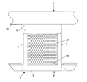
- FIG. 2 shows the principal components used to practice a preferred embodiment of the method invention and the relationship of those components to the module housing and circuit boards during the reflow soldering process.
- the bottom carrier 13 of module housing 3 partially illustrated, is shown supporting two of the upstanding metal walls, 5 and 7 , that form a compartment within the housing.
- a circuit board 15 is disposed in place in the assigned compartment defined in part by walls 5 and 7 , ready for the reflow soldering process that solders that circuit board to the bottom carrier 13 .
- Small spheres or spheroids 17 overlie circuit board 15 and fill the formed compartment, up to the top edge of the upstanding walls.
- a clamp provides a clamping force to the formed sandwich of components.
- foam sheet 19 is pressed against the edges of walls 5 and 7 , and yields or compresses along those edges, while the other portions of the foam sheet, located between the walls, presses against beads 17 .
- a portion of the foam sheet overlying the area between the walls protrudes slightly into the formed compartment.
- the foam sheet is sufficiently compressible and gives in regions thereof pressed against the edges of the relatively thick strong metal walls the foam is sufficiently rigid so as not to give significantly under the reactive force exerted by the beads, and holds the beads under pressure.
- beads 17 distribute evenly and apply pressure evenly over the entire circuit board 15 and particularly the edges of the circuit boards where soldering is most critical.
- FIG. 2 Although only a portion of the module housing and a single internal compartment is illustrated in FIG. 2, it should be realized that the beads fill all compartments within the module housing and that the metal backed foam sheet covers the entire upper end of module housing 3 . Hence what is illustrated in FIG. 2 is repeated over the entire inside of the module housing, and the clamping action described, occurs in all compartments concurrently.
- FIG. 3 illustrates the steps of the circuit board mounting process.
- a first step is to place the circuit boards through the uncovered upper end of the housing and into the assigned locations on the carrier bottom inside the module housing, as illustrated at 20 .
- beads are deposited inside the module until the entire inside is filled with the beads as represented at 22 .
- a straight spatula like a cake spatula, may be wiped across the upper edge of the housing to ensure that the glass beads do not form a mound at any particular location or deposit on the top edge of any of the internal upstanding shielding walls.
- the metal plate backed foam sheet is then placed on top of the module to cover the open end, as represented at 24 , and a clamping force is applied between the metal plate and the bottom carrier of the housing as at 26 to form a clamped assembly, thereby squeezing the beads against the circuit board and holding the circuit board flat against the bottom carrier.
- the clamped assembly is then placed in a heating chamber for reflow soldering as at 28 .
- Reflow is conventional in operation. The heat causes the solder on the rear side of the circuit board to attain the eutectic temperature and the solder melts and flows into the interstices in the adjoining metal of the bottom carrier. Thereafter the heating is terminated (or the clamped assembly is removed from the oven) and the clamped assembly is permitted to cool down, whereby the solder resolidifies and produces an attachment between the circuit boards and the carrier.
- the beads may be evacuated by a vacuum apparatus, essentially a vacuum cleaner that draws out the beads and deposits them in a container, from which the beads can later be retrieved and reused. If necessary, any remnants of beads found after vacuuming may be removed by brushing them out or agitating the housing and dumping them out. Any residue from the beads may be removed by conventional solvent cleaning.
- a vacuum apparatus essentially a vacuum cleaner that draws out the beads and deposits them in a container, from which the beads can later be retrieved and reused. If necessary, any remnants of beads found after vacuuming may be removed by brushing them out or agitating the housing and dumping them out. Any residue from the beads may be removed by conventional solvent cleaning.
- Beads 17 in this embodiment are small spheres or spheroids in shape, are sufficiently rigid to withstand the clamping force exerted by the foam sheet without significant deformation, and are capable of withstanding the effects of the incident heating encountered in the solder reflow operation without significant deformation or conduction of heat.
- the bead material should also be a relatively poor thermal conductor according to industry standards, that is, poor relative to other materials that may satisfy the preceding characteristics. The poor thermal conductivity minimizes escape of heat from the circuit board during reflow soldering (e.g., heating) that could interfere with soldering.
- the material that forms the beads should also be inorganic, so as not to adversely affect the circuit board.
- glass is the preferred material, and, more specifically borosilicate glass, such as manufactured by the MO-SCI Corporation. As those skilled in the art appreciate other materials may be substituted.
- the beads should be small enough in diameter relative to the cavity so that a large number of beads is necessary to cover the surface of the circuit board. In that way the beads should distribute the clamping force more evenly over the surface of the associated printed circuit boards. In one practical embodiment the beads are 0.10 inches in diameter.
- foam sheet 19 may be constructed from an expanded silicone elastomer material marketed by the Boyd Corporation and may be approximately one-half inch (1.27 cm) thick.
- foam sheet 19 should be modified to include grooves of a predetermined depth.
- a layout is made of all of the walls contained within the module.
- the foam sheet is then grooved in the image of that wall layout to a short depth.
- the outer dimensions of the foam sheet are such as to fit within the outer walls of the housing. Then when the sheet is overturned and aligned so that the grooves receive the edges of the walls, such as 5 and 7 , the sheet may be pressed against the beads without having to overcome the resistance of the wall edges.
- the invention is not to be construed in a limited sense. As those skilled in the art appreciate from an understanding of the foregoing description, the invention is not limited to the shape and material of the beads, the particles of the particulate used in the foregoing embodiment. Spheres and glass are at present the preferred shape and material, since glass spheres may be easily manufactured at reasonable cost. It should be clear that other shapes, as example, spheroidal or ellipsoidal, may be substituted. Further, whatever shape is chosen for the particulate, the particle may be made of glass or other material having the low thermal conductive or non-conductive property described earlier. Even pebbles or rice-shaped particles of borosilicate glass could be used in alternative embodiments of the method. All such shaped materials appear to function in the described method as equivalents.
- particulate As the reader should appreciate, the term selected as generic to all such beads is “particulate”. Webster's New Collegiate dictionary defines particulate as being “of or relating to minute separate particles”, and defines a particle as “a relatively small . . . discrete portion of something”. Thus, as used herein, the term particulate subsumes all possible shapes found to function in the described process to produce the described result.
Abstract
Description
Claims (16)
Priority Applications (2)
| Application Number | Priority Date | Filing Date | Title |
|---|---|---|---|
| US09/978,341 US6708400B2 (en) | 2001-10-15 | 2001-10-15 | Method of attaching printed circuits boards within an electronic module housing |
| US10/703,819 US7162793B2 (en) | 2001-10-15 | 2003-11-07 | Apparatus for clamping printed circuit boards inside an electronic module housing |
Applications Claiming Priority (1)
| Application Number | Priority Date | Filing Date | Title |
|---|---|---|---|
| US09/978,341 US6708400B2 (en) | 2001-10-15 | 2001-10-15 | Method of attaching printed circuits boards within an electronic module housing |
Related Child Applications (1)
| Application Number | Title | Priority Date | Filing Date |
|---|---|---|---|
| US10/703,819 Division US7162793B2 (en) | 2001-10-15 | 2003-11-07 | Apparatus for clamping printed circuit boards inside an electronic module housing |
Publications (2)
| Publication Number | Publication Date |
|---|---|
| US20030070287A1 US20030070287A1 (en) | 2003-04-17 |
| US6708400B2 true US6708400B2 (en) | 2004-03-23 |
Family
ID=25525996
Family Applications (2)
| Application Number | Title | Priority Date | Filing Date |
|---|---|---|---|
| US09/978,341 Expired - Fee Related US6708400B2 (en) | 2001-10-15 | 2001-10-15 | Method of attaching printed circuits boards within an electronic module housing |
| US10/703,819 Expired - Fee Related US7162793B2 (en) | 2001-10-15 | 2003-11-07 | Apparatus for clamping printed circuit boards inside an electronic module housing |
Family Applications After (1)
| Application Number | Title | Priority Date | Filing Date |
|---|---|---|---|
| US10/703,819 Expired - Fee Related US7162793B2 (en) | 2001-10-15 | 2003-11-07 | Apparatus for clamping printed circuit boards inside an electronic module housing |
Country Status (1)
| Country | Link |
|---|---|
| US (2) | US6708400B2 (en) |
Cited By (2)
| Publication number | Priority date | Publication date | Assignee | Title |
|---|---|---|---|---|
| US20060245151A1 (en) * | 2005-04-28 | 2006-11-02 | Kabushiki Kaisha Toshiba | Electronic device |
| US20110157806A1 (en) * | 2003-10-23 | 2011-06-30 | Sony Corporation | Electronic device |
Families Citing this family (4)
| Publication number | Priority date | Publication date | Assignee | Title |
|---|---|---|---|---|
| US7679917B2 (en) * | 2007-02-02 | 2010-03-16 | Deck Joseph F | Electronic assembly cooling |
| US8134343B2 (en) * | 2007-04-27 | 2012-03-13 | Flextronics International Kft | Energy storage device for starting engines of motor vehicles and other transportation systems |
| CN105307418B (en) * | 2015-09-07 | 2018-01-16 | 深圳市迈特迅科技有限公司 | A kind of automatically upper deduction for Wave soldering fixture |
| CN114040595B (en) * | 2021-11-12 | 2023-05-16 | 中国电子科技集团公司第三十八研究所 | Reflow soldering method and tooling for CCGA-microwave device mixed printed board assembly |
Citations (4)
| Publication number | Priority date | Publication date | Assignee | Title |
|---|---|---|---|---|
| US3604700A (en) * | 1969-06-09 | 1971-09-14 | Gault Developments Ltd R | Work-supporting devices |
| US4080729A (en) * | 1977-01-27 | 1978-03-28 | Mecklenburg Iii Alfred C | Method for transferring electrical components from a breadboard to a printed circuit board |
| US4802661A (en) * | 1988-01-20 | 1989-02-07 | Jewett Sr Bryce D | Method and apparatus for producing eyeglass frames |
| US5835359A (en) * | 1990-02-14 | 1998-11-10 | Particle Interconnect Corporation | Electrical interconnect using particle enhanced joining of metal surfaces |
-
2001
- 2001-10-15 US US09/978,341 patent/US6708400B2/en not_active Expired - Fee Related
-
2003
- 2003-11-07 US US10/703,819 patent/US7162793B2/en not_active Expired - Fee Related
Patent Citations (4)
| Publication number | Priority date | Publication date | Assignee | Title |
|---|---|---|---|---|
| US3604700A (en) * | 1969-06-09 | 1971-09-14 | Gault Developments Ltd R | Work-supporting devices |
| US4080729A (en) * | 1977-01-27 | 1978-03-28 | Mecklenburg Iii Alfred C | Method for transferring electrical components from a breadboard to a printed circuit board |
| US4802661A (en) * | 1988-01-20 | 1989-02-07 | Jewett Sr Bryce D | Method and apparatus for producing eyeglass frames |
| US5835359A (en) * | 1990-02-14 | 1998-11-10 | Particle Interconnect Corporation | Electrical interconnect using particle enhanced joining of metal surfaces |
Cited By (8)
| Publication number | Priority date | Publication date | Assignee | Title |
|---|---|---|---|---|
| US20110157806A1 (en) * | 2003-10-23 | 2011-06-30 | Sony Corporation | Electronic device |
| US8363407B2 (en) * | 2003-10-23 | 2013-01-29 | Sony Corporation | Electronic device |
| USD710840S1 (en) | 2003-10-23 | 2014-08-12 | Sony Corporation | Keyboard |
| USD759007S1 (en) | 2003-10-23 | 2016-06-14 | Sony Corporation | Keyboard |
| US20060245151A1 (en) * | 2005-04-28 | 2006-11-02 | Kabushiki Kaisha Toshiba | Electronic device |
| US7692921B2 (en) * | 2005-04-28 | 2010-04-06 | Kabushiki Kaisha Toshiba | Electronic device |
| US20100182758A1 (en) * | 2005-04-28 | 2010-07-22 | Toshio Ooe | Electronic device |
| US8009411B2 (en) | 2005-04-28 | 2011-08-30 | Kabushiki Kaisha Toshiba | Electronic device |
Also Published As
| Publication number | Publication date |
|---|---|
| US20040093723A1 (en) | 2004-05-20 |
| US7162793B2 (en) | 2007-01-16 |
| US20030070287A1 (en) | 2003-04-17 |
Similar Documents
| Publication | Publication Date | Title |
|---|---|---|
| US3816911A (en) | Shielding techniques for r.f. circuitry | |
| US7070084B2 (en) | Electrical circuit apparatus and methods for assembling same | |
| US11895769B2 (en) | Module, terminal assembly, and method for producing module | |
| US5313371A (en) | Shielding apparatus for non-conductive electronic circuit packages | |
| AU755237B2 (en) | An electrical component and an electrical circuit module having connected ground planes | |
| US6842341B1 (en) | Electrical circuit apparatus and method for assembling same | |
| US6708400B2 (en) | Method of attaching printed circuits boards within an electronic module housing | |
| US7195145B2 (en) | Electrical circuit apparatus and method for assembling same | |
| JPH08125379A (en) | Shield device | |
| KR102048809B1 (en) | Surface mounted shield device foe shielding EMI | |
| US20050151303A1 (en) | Method for producing ceramic substrate and electronic component module using ceramic substrate | |
| JPH0322554A (en) | Heat dissipation device for electronic component | |
| KR20200011393A (en) | Surface mounted shield device foe shielding EMI | |
| JP4271957B2 (en) | High frequency electronic device and manufacturing method thereof | |
| WO2004071144A1 (en) | A shield can for shielding electronic components on a pwb | |
| KR102318858B1 (en) | Mounting structure for surface mounted shield device for EMI shielding and Thermal Transferring | |
| JPH07183683A (en) | Shield structure | |
| KR20210109342A (en) | Mounting structure for surface mounted shield device | |
| JPH05327270A (en) | Electromagnetic shielding of circuit board | |
| JP2584476Y2 (en) | Printed board | |
| CN117912963A (en) | Ball planting tool, ball planting equipment and ball planting method | |
| CN111642122A (en) | Electromagnetic shielding structure and manufacturing method thereof | |
| KR20050105507A (en) | Method for producing an electronic component or module and a corresponding component or module |
Legal Events
| Date | Code | Title | Description |
|---|---|---|---|
| AS | Assignment |
Owner name: TRW INC., CALIFORNIA Free format text: ASSIGNMENT OF ASSIGNORS INTEREST;ASSIGNORS:KINTIS, MARK;TURNER, CHARLES G.;REEL/FRAME:012266/0914 Effective date: 20011015 |
|
| AS | Assignment |
Owner name: NORTHROP GRUMMAN CORPORATION, CALIFORNIA Free format text: ASSIGNMENT OF ASSIGNORS INTEREST;ASSIGNOR:TRW, INC. N/K/A NORTHROP GRUMMAN SPACE AND MISSION SYSTEMS CORPORATION, AN OHIO CORPORATION;REEL/FRAME:013751/0849 Effective date: 20030122 Owner name: NORTHROP GRUMMAN CORPORATION,CALIFORNIA Free format text: ASSIGNMENT OF ASSIGNORS INTEREST;ASSIGNOR:TRW, INC. N/K/A NORTHROP GRUMMAN SPACE AND MISSION SYSTEMS CORPORATION, AN OHIO CORPORATION;REEL/FRAME:013751/0849 Effective date: 20030122 |
|
| FEPP | Fee payment procedure |
Free format text: PAYOR NUMBER ASSIGNED (ORIGINAL EVENT CODE: ASPN); ENTITY STATUS OF PATENT OWNER: LARGE ENTITY |
|
| FPAY | Fee payment |
Year of fee payment: 4 |
|
| REMI | Maintenance fee reminder mailed | ||
| FEPP | Fee payment procedure |
Free format text: PAYER NUMBER DE-ASSIGNED (ORIGINAL EVENT CODE: RMPN); ENTITY STATUS OF PATENT OWNER: LARGE ENTITY Free format text: PAYOR NUMBER ASSIGNED (ORIGINAL EVENT CODE: ASPN); ENTITY STATUS OF PATENT OWNER: LARGE ENTITY |
|
| AS | Assignment |
Owner name: NORTHROP GRUMMAN SPACE & MISSION SYSTEMS CORP.,CAL Free format text: ASSIGNMENT OF ASSIGNORS INTEREST;ASSIGNOR:NORTHROP GRUMMAN CORPORTION;REEL/FRAME:023699/0551 Effective date: 20091125 Owner name: NORTHROP GRUMMAN SPACE & MISSION SYSTEMS CORP., CA Free format text: ASSIGNMENT OF ASSIGNORS INTEREST;ASSIGNOR:NORTHROP GRUMMAN CORPORTION;REEL/FRAME:023699/0551 Effective date: 20091125 |
|
| AS | Assignment |
Owner name: NORTHROP GRUMMAN SYSTEMS CORPORATION,CALIFORNIA Free format text: ASSIGNMENT OF ASSIGNORS INTEREST;ASSIGNOR:NORTHROP GRUMMAN SPACE & MISSION SYSTEMS CORP.;REEL/FRAME:023915/0446 Effective date: 20091210 Owner name: NORTHROP GRUMMAN SYSTEMS CORPORATION, CALIFORNIA Free format text: ASSIGNMENT OF ASSIGNORS INTEREST;ASSIGNOR:NORTHROP GRUMMAN SPACE & MISSION SYSTEMS CORP.;REEL/FRAME:023915/0446 Effective date: 20091210 |
|
| REMI | Maintenance fee reminder mailed | ||
| LAPS | Lapse for failure to pay maintenance fees | ||
| STCH | Information on status: patent discontinuation |
Free format text: PATENT EXPIRED DUE TO NONPAYMENT OF MAINTENANCE FEES UNDER 37 CFR 1.362 |
|
| FP | Lapsed due to failure to pay maintenance fee |
Effective date: 20120323 |