US6709294B1 - Electrical connector with conductive plastic features - Google Patents
Electrical connector with conductive plastic features Download PDFInfo
- Publication number
- US6709294B1 US6709294B1 US10/320,886 US32088602A US6709294B1 US 6709294 B1 US6709294 B1 US 6709294B1 US 32088602 A US32088602 A US 32088602A US 6709294 B1 US6709294 B1 US 6709294B1
- Authority
- US
- United States
- Prior art keywords
- region
- electrical connector
- electrical
- connector
- housing
- Prior art date
- Legal status (The legal status is an assumption and is not a legal conclusion. Google has not performed a legal analysis and makes no representation as to the accuracy of the status listed.)
- Expired - Lifetime
Links
Images


Classifications
-
- H—ELECTRICITY
- H01—ELECTRIC ELEMENTS
- H01R—ELECTRICALLY-CONDUCTIVE CONNECTIONS; STRUCTURAL ASSOCIATIONS OF A PLURALITY OF MUTUALLY-INSULATED ELECTRICAL CONNECTING ELEMENTS; COUPLING DEVICES; CURRENT COLLECTORS
- H01R13/00—Details of coupling devices of the kinds covered by groups H01R12/70 or H01R24/00 - H01R33/00
- H01R13/02—Contact members
- H01R13/03—Contact members characterised by the material, e.g. plating, or coating materials
-
- H—ELECTRICITY
- H01—ELECTRIC ELEMENTS
- H01R—ELECTRICALLY-CONDUCTIVE CONNECTIONS; STRUCTURAL ASSOCIATIONS OF A PLURALITY OF MUTUALLY-INSULATED ELECTRICAL CONNECTING ELEMENTS; COUPLING DEVICES; CURRENT COLLECTORS
- H01R13/00—Details of coupling devices of the kinds covered by groups H01R12/70 or H01R24/00 - H01R33/00
- H01R13/648—Protective earth or shield arrangements on coupling devices, e.g. anti-static shielding
- H01R13/658—High frequency shielding arrangements, e.g. against EMI [Electro-Magnetic Interference] or EMP [Electro-Magnetic Pulse]
- H01R13/6598—Shield material
- H01R13/6599—Dielectric material made conductive, e.g. plastic material coated with metal
Definitions
- This invention relates generally to electrical connectors and more specifically to high speed electrical connectors.
- the invention will be illustrated as applied to a board to board connector.
- the invention will be illustrated in connection with a backplane-daughter card interconnection system.
- Many electronic systems such as computer servers or telecommunications switches are built using a backplane and multiple “daughter” cards.
- the active circuitry of the electronic system is built on the daughter cards.
- a processor might be built on one daughter card.
- a memory bank might be built on a different daughter card.
- the backplane provides signal paths that route electrical signals between the daughter cards.
- electrical connectors are mounted to both the backplane and the daughter card. These connectors mate to allow electrical signals to pass between the daughter card and the backplane.
- Both of the above-described electrical connectors employ insert molding construction techniques, at least for the daughter card connectors.
- Subassemblies, called wafers are formed around individual columns of signal contacts.
- the wafers are formed by molding a dielectric material around the metal signal contacts.
- the wafers are then stacked side by side to make a connector of the desired length.
- the metal members are made from separate pieces of metal that are added to the connector.
- a metal coating be applied to the connector.
- the base material of the housing is formed of metal, usually as a die cast part. Then, insulative members are inserted to preclude the signal conductors of the connector from being shorted by the metal housing.
- a drawback of forming the shields from separate pieces of metal is that additional pieces are required to assemble the connector. The additional pieces increase the cost and complexity of manufacturing the connector.
- shield pieces are stamped and formed to create tabs or projections that extend between adjacent signal conductors. This configuration reduces the number of separate pieces because the projections stay attached to the sheet, so only one additional piece is required.
- a drawback of forming a sheet with projections extending from it is that forming the projection leaves a hole in the sheet.
- the projection increases shielding between signal conductors that are adjacent along a line running in one direction, leaving a hole in the shield sheet decreases shielding between signal conductors that are adjacent along a line running in an orthogonal direction.
- a further drawback of stamping and forming projections from a single shield member is that it is difficult to form projections that have bends or corners—which are often needed to follow contours of signal contacts in some connectors, such as right angle connectors.
- a drawback of coating metal onto a plastic is that there are no combinations of readily available and inexpensive metals and plastics that can be used. Either the metal does not adhere well to the plastic or the plastic lacks the desired thermal or mechanical properties needed to make a suitable connector.
- a further drawback of coating metal onto plastic is that available plating techniques are not selective. The portions of the connector housing which should not be conductive must be masked before the coating is applied. For example holes in the housing that hold signal contacts are often filled with plugs before coating, which are then removed after coating.
- a drawback of manufacturing connectors using a die cast metal housing is the complexity arising from the use of insulative inserts. Further, there is a limit to how thin features on a die cast part can be made. Generally, a die cast housing will have thicker parts. Using thicker housing parts is generally undesirable because it reduces the overall density of the connector. Die cast metals are more expensive than typical plastic parts.
- an electrical connector that is molded from different types of material to form at least two regions of distinct electrical properties.
- One region is formed from material filled with conducting material to alter the electrical properties.
- an electrical connector having electrical conductors in a plurality of rows wherein each of the plurality of rows includes a housing and a plurality of electrical conductors.
- Each electrical conductor has a first contact end connectable to a printed circuit board, a second contact end and an intermediate portion therebetween that is disposed within the housing.
- the housing includes a first region surrounding each of the plurality of electrical conductors, the first region made of insulative material and extending substantially along the length of the intermediate portion of the electrical conductors.
- the housing also includes a second region adjacent the first region and extending substantially along the length of the intermediate portion of the electrical conductors. The second region is made of a material with a binder containing conductive fillers.
- FIG. 1 is a sketch of an electrical connector as known in the prior art
- FIG. 2 is a sketch of a wafer of the electrical connector of FIG. 1;
- FIG. 3 is a sketch of the wafer of FIG. 2 at a stage in its manufacture
- FIGS. 4A and 4B are cross sectional views of different embodiments of a wafer of an electrical connector made according to the invention.
- FIG. 5 is a schematic illustration of a molding machine suitable for use in making a connector according to the invention.
- FIG. 6 is a sketch of a prior art backplane connector
- FIGS. 7A and 7B are views of a backplane connector made according to the invention.
- a two piece electrical connector 100 is shown to include a backplane connector 105 and a daughtercard connector 110 .
- the backplane connector 105 includes a backplane shroud 102 and a plurality of signal contacts 112 , here arranged in an array of differential signal pairs.
- the signal contacts are grouped in pairs, such as might be suitable for manufacturing a differential signal electrical connector.
- a single-ended configuration of the signal contacts 112 is also contemplated in which the signal conductors are evenly spaced.
- the backplane shroud 102 is molded from a dielectric material. Examples of such materials are liquid crystal polymer (LCP), polyphenyline sulfide (PPS), high temperature nylon or polypropylene (PPO). All of these are suitable for use as binder materials in manufacturing connectors according to the invention.
- the signal contacts 112 extend through a floor 104 of the backplane shroud 102 providing a contact area both above and below the floor 104 of the shroud 102 .
- the contact area of the signal contacts 112 above the shroud floor 104 are adapted to mate to signal contacts in daugthercard connector 110 .
- the mating contact area is in the form of a blade contact.
- a tail portion of the signal contact 112 extends below the shroud floor 104 and is adapted to mating to a printed circuit board.
- the tail portion is in the form of a press fit, “eye of the needle” compliant contact.
- other configurations are also suitable such as surface mount elements, spring contacts, solderable pins, etc.
- the backplane connector 105 mates with the daughtercard connector 110 at the blade contacts and connects with signal traces in a backplane (not shown) through the tail portions which are pressed into plated through holes in the backplane.
- the backplane shroud 102 further includes side walls 108 which extend along the length of opposing sides of the backplane shroud 102 .
- the side walls 108 include grooves 118 which run vertically along an inner surface of the side walls 108 . Grooves 118 serve to guide the daughter card connector 110 into the appropriate position in shroud 102 .
- Running parallel with the side walls 108 are a plurality of shield plates 116 , located here between rows of pairs of signal contacts 112 . In a presently preferred single ended configuration, the plurality of shield plates 116 would be located between rows of signal contacts 112 .
- other shielding configurations could be formed, including having the shield plates 116 running between the walls of the shrouds, transverse to the direction illustrated. In the prior art, the shield plates are stamped from a sheet of metal.
- Each shield plate 116 includes one or more tail portions, which extend through the shroud base 104 .
- the illustrated embodiment has tail portions formed as an “eye of the needle” compliant contact which is press fit into the backplane.
- other configurations are also suitable such as surface mount elements, spring contacts, solderable pins, etc.
- the daughtercard connector 110 is shown to include a plurality of modules or wafers 120 that are supported by a stiffener 130 .
- Each wafer 120 includes features which are inserted into apertures (not numbered) in the stiffener to locate each wafer 120 with respect to another and further to prevent rotation of the wafer 120 .
- Wafer 120 is shown to include dielectric housings 132 , 134 which are formed around both a daughtercard shield plate ( 10 , FIG. 3) and a signal lead frame.
- wafer 120 is preferably formed by first molding dielectric housing 132 around the shield plate, leaving a cavity. The signal lead frame is then inserted into the cavity and dielectric housing 134 is then overmolded on the assembly to fill the cavity.
- each wafer 120 Extending from a first edge of each wafer 120 are a plurality of signal contact tails 128 , which extend from the signal lead frame, and a plurality of shield contact tails 122 , which extend from a first edge of the shield plate. In the example of a board to board connector, these contact tails connect the signal conductors and the shield plate to a printed circuit board. In the preferred embodiment, the plurality of shield contact tails and signal contact tails 122 and 128 , respectively, on each wafer 120 are arranged in a single plane.
- both the signal contact tails 128 and the shield contact tails 122 are in the form of press fit “eye of the needle” compliants which are pressed into plated through holes located in a printed circuit board (not shown).
- the signal contact tails 128 connect to signal traces on the printed circuit board and the shield contact tails connect to a ground plane in the printed circuit board.
- the signal contact tails 128 are configured to provide a differential signal and, to that end, are arranged in pairs.
- each wafer 120 Near a second edge of each wafer 120 are mating contact regions 124 of the signal contacts which mate with the signal contacts 112 of the backplane connector 105 .
- the mating contact regions 124 are provided in the form of dual beams to mate with the blade contact end of the backplane signal contacts is 112 .
- the mating contact regions are positioned within openings in dielectric housing 132 to protect the contacts. Openings in the mating face of the wafer allow the signal contacts 112 to also enter those openings to allow mating of the daughter card and backplane signal contacts.
- shield beam contacts 126 are connected to daughter card shield plate 10 (FIG. 3) and are preferably formed from the same sheet of metal used to from the shield plate. Shield beam contacts 126 engage an upper edge of the backplane shield plate 116 when the daughter card connector 110 and backplane connector 105 are mated. In an alternate embodiment (not shown), the beam contact is provided on the backplane shield plate 116 and a blade is provided on the daughtercard shield plate between the pairs of dual beam contacts 124 . Thus, the specific shape of the shield contact is not critical to the invention.
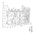
- FIG. 3 shows a wafer at an intermediate step of manufacture.
- the shield plate 10 is shown still attached to a carrier strip 310 .
- shield plates will be stamped for many wafers on a single sheet of metal. A portion of the strip of metal will be retained as a carrier strip. The individual components can then be more readily handled.
- the finished wafers 120 can then be severed from the carrier strip and assembled into daughter card connectors.
- dielectric housing 132 is shown molded over a shield. Insert molding is known in the art and is used in the connector art to provide conductors within a dielectric housing. In this prior art connector, dielectric material is molded over the majority of the surface of shield 10 . Additionally, the dielectric is largely on the upper surface of shield, leaving the lower surface of the shield exposed.
- Tabs 322 on the shield plate are visible because dielectric housing 132 is molded to leave windows 324 around tabs 322 . Likewise, holes 22 and 24 are visible because no dielectric housing has been molded around them.
- dielectric housing 132 Various features are molded into dielectric housing 132 . Cavity 350 bounded by walls 352 is left generally in the central portions of the housing 132 . Channels 324 are formed in the floor of cavity 350 by providing closely spaced projecting portions of dielectric housing. Channels 324 are used to position signal conductors. Also, openings 326 are molded to allow a mating contact area for each signal contact. The front face of dielectric housing 132 creates the mating face of the connector and contains holes to receive the mating contact portion from the backplane connector, as is known in the art. The walls of opening 326 protect the mating contact area.
- a signal lead frame is inserted into cavity 350 .
- Cavity 350 is then filled with additional dielectric material to form dielectric housing 134 , thereby locking the signal conductors into the wafer.
- Holes 22 and 24 represent openings through which stabilizers, sometimes called “pinch pins,” can be inserted into the part as dielectric housing 134 is being molded. The pinch pins hold the signal lead frame in place as the part is being molded.
- a similar molding process will be used.
- different types of material will be used in molding the housing pieces of each wafer.
- a material with different electromagnetic properties is used to form a portion of the housing for the wafer.
- portions of the housing will be formed from material that selectively alters the electrical properties of the housing, thereby suppressing cross talk, altering the impedance of the signal conductors or otherwise imparting desirable electrical properties to the connector.
- some portion of the material used to mold the connector housing will be an insulator and some portion will have a higher conductivity.
- prior art molding material will be used to create the portions of the connector housing that need to be non-conducting to avoid shorting out signal contacts or otherwise creating unfavorable electrical properties. Also, in the preferred embodiment, those portions of the connector housing for which no benefit is derived by using a material with different electromagnetic properties are also made from prior art molding materials, because such materials are generally less expensive and mechanically stronger than the electromagnetic materials to be described below.
- Prior art electrical connector molding materials are generally made from a thermoplastic binder into which non-conducting fibers are introduced for added strength, dimensional stability and to reduce the amount of higher priced binder used. Glass fibers are typical, with a loading of about 30% by volume.
- electromagnetic fillers are used in place of or in addition to the glass fibers for portions of the connector housing.
- the fillers can be conducting or can be ferroelectric, depending on the electrical properties that are desired from the material.
- a conducting filler be used.
- suitable conducting fillers are stainless steel fibers, carbon fibers, nanotube material, carbon flake or nickel-graphite powder. Blends of materials might also be used.
- the binder is loaded with conducting filler between 10% and 80% by volume. More preferably, the loading is in excess of 30% by volume. Most preferably, the conductive filler is loaded at between 40% and 60% by volume.
- the fibers When fibrous filler is used, the fibers preferably have a length between 0.5 mm and 15 mm. More preferably, the length is between 3 mm and 11 mm. In one contemplated embodiment, the fiber length is between 3 mm and 8 mm.
- the fibrous filler has a high aspect ratio (ratio of length to width).
- the fiber preferably has an aspect ratio in excess of 10 and more preferably in excess of 100.
- Filled materials can be purchased commercially, such as materials sold under the trade name Celestran® by Ticona. Or, suitable material could be custom blended as sold by RTP Company.
- the binder material is a thermoplastic material that has a reflow temperature in excess of 250° C. and more preferably in the range of 270-280° C.
- LCP and PPS are examples of suitable material.
- LCP is used because it has a lower viscosity.
- the binder material has a viscosity of less than 800 centipoise at its reflow temperature without fill. More preferably, the binder material has a viscosity of less than 400 centipoise at its reflow temperature without fill.
- the viscosity of the molding material when filled can not be made arbitrarily high.
- the material has a viscosity low enough to be molded with readily available molding machinery.
- the molding material When filled, the molding material preferably has a viscosity below 2000 centipoise at its reflow temperature and more preferably a viscosity below 1500 centipoise at its reflow temperature. It should be appreciated that the viscosity of the material can be decreased during molding operation by increasing its temperature or pressure. However, binders will break down and yield poor quality parts if heated to too high a temperature. Also, commercially available machines are limited in the amount of pressure they can generate. If the viscosity in the molding machine is too high, the material injected into the mold will set before it fills all areas of the mold.
- the binder is filled to provide a surface resistivity of less that 10 5 ⁇ /sq. More preferably, the surface resistivity is less than 10 2 ⁇ /sq. Resistivity might also be expressed as a bulk or volume resistivity. Preferably, the volume resistivity is less than 10 ⁇ -cm and more preferably less than 1 ⁇ -cm and more preferably less than 0.8 ⁇ -cm.
- housing 132 is molded with materials that contains conductive filler. If sufficiently conductive, the conductive filler acts like an extension of the shield plate 10 . Even if not fully conductive, the filled plastic can absorb signals radiating from the signal conductors that would otherwise create crosstalk.
- FIG. 4 shows a portion of wafer 120 that has been molded with two types of material according to the invention.
- housing 132 is shown formed from a material with conductive filler.
- Housing 134 is formed from an insulator with little or no conductive fillers.
- Housing 132 is electrically in contact with shield 10 , which will preferably be grounded in a connector system. Therefore, housing 132 is preferably grounded. To increase the electrical connection between housing 132 and shield plate 10 , projections can be provided from shield plate 10 .
- FIG. 4A shows, as an example, tab 460 bent out of the plane of shield plate 10 and projecting into housing 132 .
- housing 132 acts as an extension of shield 10 .
- Projections 414 A, 414 B . . . are positioned between adjacent signal conductors used to carry different signals. They therefore provide shielding between the signal conductors.
- projections 414 A, 414 B . . . are molded from plastic, they can be in almost any shape and can follow the contours of the signal conductors 410 A, 410 B . . . through the connector.
- wafer 120 is designed to carry differential signals.
- each signal is carried by a pair of signal conductors.
- each signal conductor is closer to the other conductor in its pair than it is to a conductor in an adjacent pair.
- a pair of signal conductors 410 A and 410 B carry one differential signal
- signal conductors 410 C and 410 D carry another differential signal.
- projection 414 B is positioned between these pairs to provide shielding between the adjacent differential signals.
- Projection 414 A is at the end of the column of signal conductors in wafer 120 . It is not shielding adjacent signals in the same column. However, having shielding projections at the end of the row helps prevent cross-talk from column to column.
- a second molding step is used to create insulative portions such as 450 A and 450 B in the housing. Once the signal conductors arc inserted, further dielectric material is molded over the part to finish housing 134 .
- FIG. 4B shows an alternative implementation of wafer 120 ′.
- Wafer 120 ′ is designed for single ended signals. Therefore, a projection, such as 414 B, 414 C, 414 D . . . is positioned between adjacent signal conductors, which are relatively uniformly spaced.
- insulative portions 452 A, 452 B . . . are molded between the projections 414 B, 414 C, 414 D . . . to ensure that the signal conductors are not shorted to the conducting portions of the housing.
- FIG. 5 is a simplified sketch of a machine to make a connector according to the invention.
- Molding machine 500 is a two-shot molding machine, generally as known in the art. Such machines arc used for things such as molding knobs, toohbrushes or buttons in two colors of plastic.
- Molding machine 500 has three molding chambers 510 A, 510 B and 510 C. Each molding chamber is made of a lower chamber, such as 512 A, and an upper chamber, such as 514 A. Upper chamber 514 A is moveable, allowing the upper and lower chamber to separate. As is traditional in the molding art, mold pieces separate to allow removal of molded parts or to place conducting members into the chamber to prior to injection of molding material to insert mold the conducting members into the molding material.
- the lower chambers 512 A, 512 B and 512 C are identical. Each lower chamber has a mold cavity that has the same contour as the lower portions of the part to be molded.
- Upper chamber 514 A is shaped to mate with any of the lower chambers and form a mold cavity that ha contour matching the desired contour of the part being molded after one type of molding material has been applied.
- mold chamber 510 A has a contour that matches shield 10 with housing 132 molded on it—but without housing 134 in place.
- Mold chamber 510 B has a contour that matches the upper surface of housing 132 with inserts 450 A and 450 B in place.
- Mold chamber 510 C has a contour that matches the contour of the finished part. To provide this result, upper chamber 514 B will have a different shape than upper chamber 514 A. In the example of FIG. 4, mold chamber 510 C will have a contour that matches the contour of the finished wafer 120 with a shield 10 , housing 132 and 134 in place.
- Molding machine 500 includes feed systems 520 A, 520 B and 520 C. As in a conventional molding machine, each of the feed systems provides molding material into a mold cavity. In a preferred embodiment that uses a thermoplastic material as a binder, each feed system includes a hopper of materials in pellet form.
- material is dispensed from the hopper and heated to a liquid state.
- the feed system then injects the liquid material into the mold cavity.
- auger screw can be used to provide the required force to inject the material.
- the material passes through nozzles 522 A, 522 B or 522 C into a respective mold chamber 510 A, 510 B or 510 C.
- the material rapidly cools to below its set point.
- the mold can then be opened. Parts molded in chamber 510 A and 510 B are only partially complete.
- the partially finished part is left in lower chamber 512 A.
- Lower chamber 512 A is then moved below upper chamber 514 B.
- the partially molded part is in chamber 510 B. Additional material can be added to the part.
- the partially finished part can then be rotated below upper chamber 514 C to complete the operation.
- lower mold chamber 512 A is mounted on a moving member and moves with the partially molded part into position to form mold chamber 510 B.
- lower mold chamber 512 A rotates on a turntable-like device.
- other forms of moving members could be used.
- a moving member that provided linear motion might be preferred.
- a shuttle is a suitable moving member that provides linear motion.
- a shuttle-type arrangement would be preferable.
- numerous shield plates would be stamped from a long strip of metal.
- a carrier strip would be left and each of the shield plates would be attached to the carrier strip.
- the strip would be wound on a reel.
- the reel would feed shields one at a time into chamber 510 A. For each cycle of the molding machine, a new shield would be fed into chamber 510 A and a finished part would emerge from chamber 510 B. The finished parts, still on their carrier strips, could then be wound on another reel.
- feed system 520 A feeds molding material filled with conducting fibers.
- such a material is likely to have a higher viscosity than materials traditionally used to mold connector housings. Consequently, greater pressure might be required.
- Feed system 520 A must generate sufficient force to inject the filled material. In practice, empirical data is gathered to determined the appropriate settings for molding machine 500 . However, it is expected that the feed system providing conductor filled plastic will deliver material at a higher pressure.
- nozzle 522 A which delivers the conductor filled plastic at higher pressure will have a larger orifice. Furthermore, the combination of higher pressure and conductive fillers, which could be abrasive, is likely to cause additional wear in feed system 520 A. To counteract these problems, nozzle 522 A is preferably made of a hardened material, such as carbide steel.
- molding machine 500 exposed to the conductor filled plastic are also likely to experience excessive wear and can likewise be made of hardened materials and might be made easily replaceable.
- carbide mold inserts might be used to reduce wear and also to allow easy replacement.
- FIG. 6 shows a prior art backplane connector 605 .
- Backplane connector 605 has a shroud 610 .
- shroud 610 is die cast of metal.
- Shields 616 may make direct electrical contact to the metal housing, as both are intended to be connected to ground in operation. However, signal conductors 612 would be shorted out if inserted directly into the metal housing. Insulative spacer member 620 is inserted into shroud 610 to prevent signal conductors 612 from being shorted out by the conducting housing of backplane connector 605 .
- the implementation shown in FIG. 6 has the drawback of being made of relatively expensive die cast parts and has separate pieces that add cost to the assembly operation. Using the molding technique according to the invention, a connector providing similar performance can be achieved at a lower cost.
- FIG. 7A shows a portion of backplane connector 605 in cross section.
- Housing 632 is molded of conventional connector molding material.
- the thermoplastic PPS filled to 30% by volume with glass fiber might be used.
- recessed area is left for housing 634 .
- the recessed area includes lands 710 (FIG. 7B) that contain areas for receiving signal conductors 612 .
- the recessed area is filled with molding material with conductive filler.
- molding material with conductive filler. Examples of the materials and fillers that might be used for housing 634 are given above.
- FIG. 7A shows a projection 650 from shield 616 into the conductive portion 634 .
- the projection enhances the electrical conductivity between the shield and the conducting plastic portions.
- the projection could be in any convenient form, such as a tab or a bend in the shield.
- FIG. 7B shows a top view of the portion of backplane connector 605 shown in FIG. 7 A. Lands 710 are visible in this view. Also, it can be seen that housing 634 is in contact with shields 616 , grounding housing 634 through the ground contacts of shields 616 .
- the invention was described as applied to a backplane-daughter card connector.
- Conductive features might be built into connectors in any configuration, such as stacking connectors or other board to board connectors or in phone jacks or cable connectors.
- the invention was illustrated as applied to both the backplane and daughter card pieces of the connector. It could be used with either or both.
- a two step molding operation is described in connection with the backplane connector and a three step operation is described in connection with daughter card wafers 120 .
- Other types of molding operations might be used.
- a single step molding might be used in cases where the entire housing is to be conducting.
- three or more molding steps might be performed. Such a process might be employed where the finished shape of the part is more complicated than can be molded in two steps or where materials with more than two different properties are required in the finished product.
- a conductive housing is molded and then an insulative housing is molded. Thereafter, the signal contacts are inserted and a second insulative layer is applied to lock the signal contacts into place.
- Application of the second insulative layer could be done as a true molding operation using a mold with a cavity shaped to match the desired final contour of the part. Alternatively, a simpler form of “molding” might be used in which the first two operations leave a cavity. Once the signal contacts are inserted into this cavity the second insulative layer is “molded” by putting material into this cavity and leveling it off to leave a smooth upper surface. In this process, a full cavity mold is not required to shape the final part.
- FIG. 5 shows a molding machine that has two mold chambers operating simultaneously. For each cycle of the molding machine, a part is being molded with the first type material and another part is being molded with the second type of material. One complete part can therefore emerge from mold chamber 510 B each cycle. As shown, there is no loss of efficiency from having a two step molding operation. It would be possible, however, to manufacture parts with molding steps done sequentially rather than simultaneously. Sequential molding equipment might be lower cost, but would have lower throughput.
Abstract
Description
Claims (22)
Priority Applications (5)
| Application Number | Priority Date | Filing Date | Title |
|---|---|---|---|
| US10/320,886 US6709294B1 (en) | 2002-12-17 | 2002-12-17 | Electrical connector with conductive plastic features |
| DE60326013T DE60326013D1 (en) | 2002-12-17 | 2003-12-17 | ELECTRICAL PLUG CONNECTOR WITH CONDUCTIVE PLASTIC ELEMENTS |
| PCT/US2003/039993 WO2004059794A2 (en) | 2002-12-17 | 2003-12-17 | Electrical connector with conductive plastic features |
| AU2003297164A AU2003297164A1 (en) | 2002-12-17 | 2003-12-17 | Electrical connector with conductive plastic features |
| EP03814022A EP1611641B1 (en) | 2002-12-17 | 2003-12-17 | Electrical connector with conductive plastic features |
Applications Claiming Priority (1)
| Application Number | Priority Date | Filing Date | Title |
|---|---|---|---|
| US10/320,886 US6709294B1 (en) | 2002-12-17 | 2002-12-17 | Electrical connector with conductive plastic features |
Publications (1)
| Publication Number | Publication Date |
|---|---|
| US6709294B1 true US6709294B1 (en) | 2004-03-23 |
Family
ID=31978087
Family Applications (1)
| Application Number | Title | Priority Date | Filing Date |
|---|---|---|---|
| US10/320,886 Expired - Lifetime US6709294B1 (en) | 2002-12-17 | 2002-12-17 | Electrical connector with conductive plastic features |
Country Status (5)
| Country | Link |
|---|---|
| US (1) | US6709294B1 (en) |
| EP (1) | EP1611641B1 (en) |
| AU (1) | AU2003297164A1 (en) |
| DE (1) | DE60326013D1 (en) |
| WO (1) | WO2004059794A2 (en) |
Cited By (128)
| Publication number | Priority date | Publication date | Assignee | Title |
|---|---|---|---|---|
| US20040161974A1 (en) * | 2002-05-06 | 2004-08-19 | Lang Harold Keith | High-speed differential signal connector particularly suitable for docking applications |
| US6986682B1 (en) | 2005-05-11 | 2006-01-17 | Myoungsoo Jeon | High speed connector assembly with laterally displaceable head portion |
| US20060068640A1 (en) * | 2004-09-30 | 2006-03-30 | Teradyne, Inc. | High speed, high density electrical connector |
| US20060110983A1 (en) * | 2004-11-24 | 2006-05-25 | Muench Frank J | Visible power connection |
| US20070004282A1 (en) * | 2005-06-30 | 2007-01-04 | Teradyne, Inc. | High speed high density electrical connector |
| US20070042639A1 (en) * | 2005-06-30 | 2007-02-22 | Manter David P | Connector with improved shielding in mating contact region |
| US20070160771A1 (en) * | 2006-01-10 | 2007-07-12 | Engineered Products And Services, Inc. | Electrically-conductive plastic hangers |
| US20070158287A1 (en) * | 2006-01-10 | 2007-07-12 | Engineered Products & Services, Inc. | Electrically-Conductive Plastic Hangers |
| US20070293073A1 (en) * | 2005-11-14 | 2007-12-20 | Hughes David C | Separable loadbreak connector and system |
| US20080030970A1 (en) * | 2003-06-24 | 2008-02-07 | Payne Jason J | Printed circuit board for high speed, high density electrical connector with improved cross-talk minimization, attenuation and impedance mismatch characteristics |
| US20080096433A1 (en) * | 2006-06-30 | 2008-04-24 | Molex Incorporated | Differential pair electrical connector having crosstalk shield tabs |
| US20080108233A1 (en) * | 2006-11-07 | 2008-05-08 | Myoungsoo Jeon | Connector having self-adjusting surface-mount attachment structures |
| US20080192409A1 (en) * | 2007-02-13 | 2008-08-14 | Paul Michael Roscizewski | Livebreak fuse removal assembly for deadfront electrical apparatus |
| US20080200053A1 (en) * | 2007-02-20 | 2008-08-21 | David Charles Hughes | Thermoplastic interface and shield assembly for separable insulated connector system |
| US20080207022A1 (en) * | 2007-02-22 | 2008-08-28 | David Charles Hughes | Medium voltage separable insulated energized break connector |
| US20080220638A1 (en) * | 2005-08-08 | 2008-09-11 | David Charles Hughes | Apparatus, System and Methods for Deadfront Visible Loadbreak |
| US20080233786A1 (en) * | 2007-03-20 | 2008-09-25 | David Charles Hughes | Separable loadbreak connector and system |
| US20080248658A1 (en) * | 2007-04-04 | 2008-10-09 | Cohen Thomas S | Electrical connector lead frame |
| US20080248659A1 (en) * | 2007-04-04 | 2008-10-09 | Cohen Thomas S | Electrical connector with complementary conductive elements |
| US20080259532A1 (en) * | 2007-04-23 | 2008-10-23 | Cooper Technologies Company | Switchgear Bus Support System and Method |
| US20080261465A1 (en) * | 2007-04-23 | 2008-10-23 | Cooper Technologies Company | Separable Insulated Connector System |
| US20090073382A1 (en) * | 2006-03-10 | 2009-03-19 | Mark Bischoff | Devices and Methods for Defined Orientation of an Eye |
| US20090100675A1 (en) * | 2007-02-20 | 2009-04-23 | Cooper Technologies Company | Method for manufacturing a shield housing for a separable connector |
| US20090108847A1 (en) * | 2007-10-31 | 2009-04-30 | Cooper Technologies Company | Fully Insulated Fuse Test and Ground Device |
| US20090111324A1 (en) * | 2007-02-20 | 2009-04-30 | Cooper Technologies Company | Shield Housing for a Separable Connector |
| US20090215313A1 (en) * | 2008-02-25 | 2009-08-27 | Cooper Technologies Company | Separable connector with reduced surface contact |
| US20090215321A1 (en) * | 2008-02-25 | 2009-08-27 | Cooper Technologies Company | Push-then-pull operation of a separable connector system |
| US20090233472A1 (en) * | 2008-03-12 | 2009-09-17 | David Charles Hughes | Electrical Connector with Fault Closure Lockout |
| US20090255106A1 (en) * | 2008-04-11 | 2009-10-15 | Cooper Technologies Company | Method of using an extender for a separable insulated connector |
| US20090258547A1 (en) * | 2008-04-11 | 2009-10-15 | Cooper Technologies Company | Extender for a separable insulated connector |
| US20090291592A1 (en) * | 2006-06-30 | 2009-11-26 | Molex Incorporated | Connector with insert for reduced crosstalk |
| US20090291593A1 (en) * | 2005-06-30 | 2009-11-26 | Prescott Atkinson | High frequency broadside-coupled electrical connector |
| US7661979B2 (en) | 2007-06-01 | 2010-02-16 | Cooper Technologies Company | Jacket sleeve with grippable tabs for a cable connector |
| US7670162B2 (en) | 2008-02-25 | 2010-03-02 | Cooper Technologies Company | Separable connector with interface undercut |
| US7722401B2 (en) | 2007-04-04 | 2010-05-25 | Amphenol Corporation | Differential electrical connector with skew control |
| US20100144165A1 (en) * | 2008-12-05 | 2010-06-10 | Fowler David K | Electrical Connector System |
| US20100144174A1 (en) * | 2008-12-05 | 2010-06-10 | Glover Douglas W | Electrical Connector System |
| US20100144176A1 (en) * | 2008-12-05 | 2010-06-10 | James Lee Fedder | Electrical Connector System |
| US20100144169A1 (en) * | 2008-12-05 | 2010-06-10 | Glover Douglas W | Electrical connector system |
| US20100144168A1 (en) * | 2008-12-05 | 2010-06-10 | Glover Douglas W | Electrical Connector System |
| US20100144203A1 (en) * | 2008-12-05 | 2010-06-10 | Glover Douglas W | Electrical connector system |
| US20100144167A1 (en) * | 2008-12-05 | 2010-06-10 | Fedder James L | Electrical Connector System |
| US20100144201A1 (en) * | 2008-12-05 | 2010-06-10 | Defibaugh George R | Electrical connector system |
| US20100144175A1 (en) * | 2008-12-05 | 2010-06-10 | Helster David W | Electrical connector system |
| US20100144204A1 (en) * | 2008-12-05 | 2010-06-10 | John Edward Knaub | Electrical connector system |
| US20100151726A1 (en) * | 2008-12-05 | 2010-06-17 | James Lee Fedder | Electrical Connector System |
| US20100151741A1 (en) * | 2008-12-05 | 2010-06-17 | James Lee Fedder | Electrical Connector System |
| US20100240233A1 (en) * | 2009-03-19 | 2010-09-23 | Johnescu Douglas M | Electrical connector having ribbed ground plate |
| US20110067237A1 (en) * | 2009-09-09 | 2011-03-24 | Cohen Thomas S | Compressive contact for high speed electrical connector |
| US20110195607A1 (en) * | 2008-09-30 | 2011-08-11 | Jeroen De Bruijn | Lead frame assembly for an electrical connector |
| US20110223807A1 (en) * | 2010-03-15 | 2011-09-15 | Tyco Electronics Corporation | Connector assembly having a compensation circuit component |
| US8056226B2 (en) | 2008-02-25 | 2011-11-15 | Cooper Technologies Company | Method of manufacturing a dual interface separable insulated connector with overmolded faraday cage |
| US8109776B2 (en) | 2008-02-27 | 2012-02-07 | Cooper Technologies Company | Two-material separable insulated connector |
| US8172614B2 (en) | 2009-02-04 | 2012-05-08 | Amphenol Corporation | Differential electrical connector with improved skew control |
| US20120129395A1 (en) * | 2010-11-19 | 2012-05-24 | Wayne Samuel Davis | Electrical Connector System |
| US8231415B2 (en) | 2009-07-10 | 2012-07-31 | Fci Americas Technology Llc | High speed backplane connector with impedance modification and skew correction |
| US8298015B2 (en) | 2008-10-10 | 2012-10-30 | Amphenol Corporation | Electrical connector assembly with improved shield and shield coupling |
| US8382520B2 (en) | 2011-01-17 | 2013-02-26 | Tyco Electronics Corporation | Connector assembly |
| US8491313B2 (en) | 2011-02-02 | 2013-07-23 | Amphenol Corporation | Mezzanine connector |
| US8727791B2 (en) | 2008-01-17 | 2014-05-20 | Amphenol Corporation | Electrical connector assembly |
| US8771016B2 (en) | 2010-02-24 | 2014-07-08 | Amphenol Corporation | High bandwidth connector |
| US8814595B2 (en) | 2011-02-18 | 2014-08-26 | Amphenol Corporation | High speed, high density electrical connector |
| USD718253S1 (en) | 2012-04-13 | 2014-11-25 | Fci Americas Technology Llc | Electrical cable connector |
| US8905651B2 (en) | 2012-01-31 | 2014-12-09 | Fci | Dismountable optical coupling device |
| USD720698S1 (en) | 2013-03-15 | 2015-01-06 | Fci Americas Technology Llc | Electrical cable connector |
| US8926377B2 (en) | 2009-11-13 | 2015-01-06 | Amphenol Corporation | High performance, small form factor connector with common mode impedance control |
| US8944831B2 (en) | 2012-04-13 | 2015-02-03 | Fci Americas Technology Llc | Electrical connector having ribbed ground plate with engagement members |
| US8961227B2 (en) | 2011-02-07 | 2015-02-24 | Amphenol Corporation | Connector having improved contacts |
| US8961229B2 (en) | 2012-02-22 | 2015-02-24 | Hon Hai Precision Industry Co., Ltd. | High speed high density connector assembly |
| US9004942B2 (en) | 2011-10-17 | 2015-04-14 | Amphenol Corporation | Electrical connector with hybrid shield |
| USD727268S1 (en) | 2012-04-13 | 2015-04-21 | Fci Americas Technology Llc | Vertical electrical connector |
| USD727852S1 (en) | 2012-04-13 | 2015-04-28 | Fci Americas Technology Llc | Ground shield for a right angle electrical connector |
| US9022806B2 (en) | 2012-06-29 | 2015-05-05 | Amphenol Corporation | Printed circuit board for RF connector mounting |
| US20150188250A1 (en) * | 2013-12-27 | 2015-07-02 | Foxconn Interconnect Technology Limited | Electrical connector with an improved terminal base |
| USD733662S1 (en) | 2013-01-25 | 2015-07-07 | Fci Americas Technology Llc | Connector housing for electrical connector |
| USD746236S1 (en) | 2012-07-11 | 2015-12-29 | Fci Americas Technology Llc | Electrical connector housing |
| US9257778B2 (en) | 2012-04-13 | 2016-02-09 | Fci Americas Technology | High speed electrical connector |
| CN105470736A (en) * | 2014-08-27 | 2016-04-06 | 富士康(昆山)电脑接插件有限公司 | Electric connector |
| US9450344B2 (en) | 2014-01-22 | 2016-09-20 | Amphenol Corporation | High speed, high density electrical connector with shielded signal paths |
| US9484674B2 (en) | 2013-03-14 | 2016-11-01 | Amphenol Corporation | Differential electrical connector with improved skew control |
| US9490587B1 (en) | 2015-12-14 | 2016-11-08 | Tyco Electronics Corporation | Communication connector having a contact module stack |
| US9520689B2 (en) | 2013-03-13 | 2016-12-13 | Amphenol Corporation | Housing for a high speed electrical connector |
| US9543703B2 (en) | 2012-07-11 | 2017-01-10 | Fci Americas Technology Llc | Electrical connector with reduced stack height |
| CN106374311A (en) * | 2016-09-14 | 2017-02-01 | 安费诺商用电子产品(成都)有限公司 | Manufacturing method for conductive plastic assembly, conductive plastic assembly, and card-plugging type connector |
| US9691514B2 (en) * | 2015-01-22 | 2017-06-27 | Delphi Technologies, Inc. | Electrical assembly having a fibrous conductive interface between a conductive composite component and a metallic component |
| US9831588B2 (en) | 2012-08-22 | 2017-11-28 | Amphenol Corporation | High-frequency electrical connector |
| US9859658B2 (en) | 2015-05-14 | 2018-01-02 | Te Connectivity Corporation | Electrical connector having resonance controlled ground conductors |
| US10122129B2 (en) | 2010-05-07 | 2018-11-06 | Amphenol Corporation | High performance cable connector |
| US10205286B2 (en) | 2016-10-19 | 2019-02-12 | Amphenol Corporation | Compliant shield for very high speed, high density electrical interconnection |
| US10243304B2 (en) | 2016-08-23 | 2019-03-26 | Amphenol Corporation | Connector configurable for high performance |
| US10541482B2 (en) | 2015-07-07 | 2020-01-21 | Amphenol Fci Asia Pte. Ltd. | Electrical connector with cavity between terminals |
| US10601181B2 (en) | 2017-12-01 | 2020-03-24 | Amphenol East Asia Ltd. | Compact electrical connector |
| US10644455B1 (en) | 2019-01-17 | 2020-05-05 | Te Connectivity Corporation | Electrical connector with absorber member |
| US10651603B2 (en) | 2016-06-01 | 2020-05-12 | Amphenol Fci Connectors Singapore Pte. Ltd. | High speed electrical connector |
| US10777921B2 (en) * | 2017-12-06 | 2020-09-15 | Amphenol East Asia Ltd. | High speed card edge connector |
| US10840649B2 (en) | 2014-11-12 | 2020-11-17 | Amphenol Corporation | Organizer for a very high speed, high density electrical interconnection system |
| US10879643B2 (en) | 2015-07-23 | 2020-12-29 | Amphenol Corporation | Extender module for modular connector |
| US10931062B2 (en) | 2018-11-21 | 2021-02-23 | Amphenol Corporation | High-frequency electrical connector |
| US10944189B2 (en) | 2018-09-26 | 2021-03-09 | Amphenol East Asia Electronic Technology (Shenzhen) Co., Ltd. | High speed electrical connector and printed circuit board thereof |
| US10965064B2 (en) | 2019-04-22 | 2021-03-30 | Amphenol East Asia Ltd. | SMT receptacle connector with side latching |
| US11070006B2 (en) | 2017-08-03 | 2021-07-20 | Amphenol Corporation | Connector for low loss interconnection system |
| US11101611B2 (en) | 2019-01-25 | 2021-08-24 | Fci Usa Llc | I/O connector configured for cabled connection to the midboard |
| US11189971B2 (en) | 2019-02-14 | 2021-11-30 | Amphenol East Asia Ltd. | Robust, high-frequency electrical connector |
| US11189943B2 (en) | 2019-01-25 | 2021-11-30 | Fci Usa Llc | I/O connector configured for cable connection to a midboard |
| US11205877B2 (en) | 2018-04-02 | 2021-12-21 | Ardent Concepts, Inc. | Controlled-impedance compliant cable termination |
| US11217942B2 (en) | 2018-11-15 | 2022-01-04 | Amphenol East Asia Ltd. | Connector having metal shell with anti-displacement structure |
| US11381015B2 (en) | 2018-12-21 | 2022-07-05 | Amphenol East Asia Ltd. | Robust, miniaturized card edge connector |
| US11437762B2 (en) | 2019-02-22 | 2022-09-06 | Amphenol Corporation | High performance cable connector assembly |
| US11444398B2 (en) | 2018-03-22 | 2022-09-13 | Amphenol Corporation | High density electrical connector |
| US11469553B2 (en) | 2020-01-27 | 2022-10-11 | Fci Usa Llc | High speed connector |
| US11569613B2 (en) | 2021-04-19 | 2023-01-31 | Amphenol East Asia Ltd. | Electrical connector having symmetrical docking holes |
| US11588277B2 (en) | 2019-11-06 | 2023-02-21 | Amphenol East Asia Ltd. | High-frequency electrical connector with lossy member |
| US11637391B2 (en) | 2020-03-13 | 2023-04-25 | Amphenol Commercial Products (Chengdu) Co., Ltd. | Card edge connector with strength member, and circuit board assembly |
| US11652307B2 (en) | 2020-08-20 | 2023-05-16 | Amphenol East Asia Electronic Technology (Shenzhen) Co., Ltd. | High speed connector |
| US11670879B2 (en) | 2020-01-28 | 2023-06-06 | Fci Usa Llc | High frequency midboard connector |
| US11710917B2 (en) | 2017-10-30 | 2023-07-25 | Amphenol Fci Asia Pte. Ltd. | Low crosstalk card edge connector |
| US11728585B2 (en) | 2020-06-17 | 2023-08-15 | Amphenol East Asia Ltd. | Compact electrical connector with shell bounding spaces for receiving mating protrusions |
| US11735852B2 (en) | 2019-09-19 | 2023-08-22 | Amphenol Corporation | High speed electronic system with midboard cable connector |
| US11742601B2 (en) | 2019-05-20 | 2023-08-29 | Amphenol Corporation | High density, high speed electrical connector |
| USD1002553S1 (en) | 2021-11-03 | 2023-10-24 | Amphenol Corporation | Gasket for connector |
| US11799246B2 (en) | 2020-01-27 | 2023-10-24 | Fci Usa Llc | High speed connector |
| US11799230B2 (en) | 2019-11-06 | 2023-10-24 | Amphenol East Asia Ltd. | High-frequency electrical connector with in interlocking segments |
| US11817655B2 (en) | 2020-09-25 | 2023-11-14 | Amphenol Commercial Products (Chengdu) Co., Ltd. | Compact, high speed electrical connector |
| US11817639B2 (en) | 2020-08-31 | 2023-11-14 | Amphenol Commercial Products (Chengdu) Co., Ltd. | Miniaturized electrical connector for compact electronic system |
| US11831106B2 (en) | 2016-05-31 | 2023-11-28 | Amphenol Corporation | High performance cable termination |
| US11831092B2 (en) | 2020-07-28 | 2023-11-28 | Amphenol East Asia Ltd. | Compact electrical connector |
| US11870171B2 (en) | 2018-10-09 | 2024-01-09 | Amphenol Commercial Products (Chengdu) Co., Ltd. | High-density edge connector |
| US11942716B2 (en) | 2020-09-22 | 2024-03-26 | Amphenol Commercial Products (Chengdu) Co., Ltd. | High speed electrical connector |
Citations (7)
| Publication number | Priority date | Publication date | Assignee | Title |
|---|---|---|---|---|
| US4195272A (en) * | 1978-02-06 | 1980-03-25 | Bunker Ramo Corporation | Filter connector having contact strain relief means and an improved ground plate structure and method of fabricating same |
| US4276523A (en) * | 1979-08-17 | 1981-06-30 | Bunker Ramo Corporation | High density filter connector |
| US4682129A (en) * | 1983-03-30 | 1987-07-21 | E. I. Du Pont De Nemours And Company | Thick film planar filter connector having separate ground plane shield |
| US4761147A (en) * | 1987-02-02 | 1988-08-02 | I.G.G. Electronics Canada Inc. | Multipin connector with filtering |
| US5551893A (en) * | 1994-05-10 | 1996-09-03 | Osram Sylvania Inc. | Electrical connector with grommet and filter |
| US6174203B1 (en) * | 1998-07-03 | 2001-01-16 | Sumitomo Wiring Sysytems, Ltd. | Connector with housing insert molded to a magnetic element |
| US6364711B1 (en) * | 2000-10-20 | 2002-04-02 | Molex Incorporated | Filtered electrical connector |
Family Cites Families (1)
| Publication number | Priority date | Publication date | Assignee | Title |
|---|---|---|---|---|
| AU1921000A (en) * | 1999-11-24 | 2001-06-04 | Teradyne, Inc. | Differential signal electrical connectors |
-
2002
- 2002-12-17 US US10/320,886 patent/US6709294B1/en not_active Expired - Lifetime
-
2003
- 2003-12-17 DE DE60326013T patent/DE60326013D1/en not_active Expired - Lifetime
- 2003-12-17 WO PCT/US2003/039993 patent/WO2004059794A2/en not_active Application Discontinuation
- 2003-12-17 EP EP03814022A patent/EP1611641B1/en not_active Expired - Lifetime
- 2003-12-17 AU AU2003297164A patent/AU2003297164A1/en not_active Abandoned
Patent Citations (7)
| Publication number | Priority date | Publication date | Assignee | Title |
|---|---|---|---|---|
| US4195272A (en) * | 1978-02-06 | 1980-03-25 | Bunker Ramo Corporation | Filter connector having contact strain relief means and an improved ground plate structure and method of fabricating same |
| US4276523A (en) * | 1979-08-17 | 1981-06-30 | Bunker Ramo Corporation | High density filter connector |
| US4682129A (en) * | 1983-03-30 | 1987-07-21 | E. I. Du Pont De Nemours And Company | Thick film planar filter connector having separate ground plane shield |
| US4761147A (en) * | 1987-02-02 | 1988-08-02 | I.G.G. Electronics Canada Inc. | Multipin connector with filtering |
| US5551893A (en) * | 1994-05-10 | 1996-09-03 | Osram Sylvania Inc. | Electrical connector with grommet and filter |
| US6174203B1 (en) * | 1998-07-03 | 2001-01-16 | Sumitomo Wiring Sysytems, Ltd. | Connector with housing insert molded to a magnetic element |
| US6364711B1 (en) * | 2000-10-20 | 2002-04-02 | Molex Incorporated | Filtered electrical connector |
Cited By (278)
| Publication number | Priority date | Publication date | Assignee | Title |
|---|---|---|---|---|
| US20040161974A1 (en) * | 2002-05-06 | 2004-08-19 | Lang Harold Keith | High-speed differential signal connector particularly suitable for docking applications |
| US6918789B2 (en) * | 2002-05-06 | 2005-07-19 | Molex Incorporated | High-speed differential signal connector particularly suitable for docking applications |
| US20080030970A1 (en) * | 2003-06-24 | 2008-02-07 | Payne Jason J | Printed circuit board for high speed, high density electrical connector with improved cross-talk minimization, attenuation and impedance mismatch characteristics |
| US7508681B2 (en) | 2003-06-24 | 2009-03-24 | Amphenol Corporation | Printed circuit board for high speed, high density electrical connector with improved cross-talk minimization attenuation and impedance mismatch characteristics |
| US20110003509A1 (en) * | 2004-09-30 | 2011-01-06 | Gailus Mark W | High speed, high density electrical connector |
| WO2006039277A1 (en) * | 2004-09-30 | 2006-04-13 | Amphenol Corporation | High speed, high density electrical connector |
| US20080194146A1 (en) * | 2004-09-30 | 2008-08-14 | Amphenol Corporation | High Speed, High Density Electrical Connector |
| US7771233B2 (en) | 2004-09-30 | 2010-08-10 | Amphenol Corporation | High speed, high density electrical connector |
| EP2262061A1 (en) | 2004-09-30 | 2010-12-15 | Amphenol Corporation | High speed, high density electrical connector |
| US9300074B2 (en) | 2004-09-30 | 2016-03-29 | Amphenol Corporation | High speed, high density electrical connector |
| US7371117B2 (en) | 2004-09-30 | 2008-05-13 | Amphenol Corporation | High speed, high density electrical connector |
| US9899774B2 (en) | 2004-09-30 | 2018-02-20 | Amphenol Corporation | High speed, high density electrical connector |
| CN102176586B (en) * | 2004-09-30 | 2012-11-28 | 安费诺公司 | Electrical connector and electronic system |
| US8371875B2 (en) | 2004-09-30 | 2013-02-12 | Amphenol Corporation | High speed, high density electrical connector |
| US20180166828A1 (en) * | 2004-09-30 | 2018-06-14 | Amphenol Corporation | High speed, high density electrical connector |
| US20060068640A1 (en) * | 2004-09-30 | 2006-03-30 | Teradyne, Inc. | High speed, high density electrical connector |
| US20060110983A1 (en) * | 2004-11-24 | 2006-05-25 | Muench Frank J | Visible power connection |
| US7182647B2 (en) * | 2004-11-24 | 2007-02-27 | Cooper Technologies Company | Visible break assembly including a window to view a power connection |
| US6986682B1 (en) | 2005-05-11 | 2006-01-17 | Myoungsoo Jeon | High speed connector assembly with laterally displaceable head portion |
| US7121889B1 (en) | 2005-05-11 | 2006-10-17 | Myoungsoo Jeon | High speed connector assembly with laterally displaceable head portion |
| US8998642B2 (en) * | 2005-06-30 | 2015-04-07 | Amphenol Corporation | Connector with improved shielding in mating contact region |
| CN101273501B (en) * | 2005-06-30 | 2011-02-09 | 安费诺公司 | Sheet of electrical connector with multi-sheet and its forming method |
| US20070004282A1 (en) * | 2005-06-30 | 2007-01-04 | Teradyne, Inc. | High speed high density electrical connector |
| WO2007005599A1 (en) * | 2005-06-30 | 2007-01-11 | Amphenol Corporation | High speed, high density electrical connector |
| US7163421B1 (en) * | 2005-06-30 | 2007-01-16 | Amphenol Corporation | High speed high density electrical connector |
| US9219335B2 (en) * | 2005-06-30 | 2015-12-22 | Amphenol Corporation | High frequency electrical connector |
| US9705255B2 (en) | 2005-06-30 | 2017-07-11 | Amphenol Corporation | High frequency electrical connector |
| US20090291593A1 (en) * | 2005-06-30 | 2009-11-26 | Prescott Atkinson | High frequency broadside-coupled electrical connector |
| US7335063B2 (en) | 2005-06-30 | 2008-02-26 | Amphenol Corporation | High speed, high density electrical connector |
| WO2007005597A3 (en) * | 2005-06-30 | 2007-12-27 | Amphenol Corp | Connector with improved shielding in mating contact region |
| US7753731B2 (en) | 2005-06-30 | 2010-07-13 | Amphenol TCS | High speed, high density electrical connector |
| CN102882097B (en) * | 2005-06-30 | 2019-05-14 | 安费诺公司 | The connector with improved shielding in cooperation contact area |
| US8864521B2 (en) * | 2005-06-30 | 2014-10-21 | Amphenol Corporation | High frequency electrical connector |
| US20090011641A1 (en) * | 2005-06-30 | 2009-01-08 | Amphenol Corporation | High speed, high density electrical connector |
| US20070042639A1 (en) * | 2005-06-30 | 2007-02-22 | Manter David P | Connector with improved shielding in mating contact region |
| US8083553B2 (en) * | 2005-06-30 | 2011-12-27 | Amphenol Corporation | Connector with improved shielding in mating contact region |
| US20120156929A1 (en) * | 2005-06-30 | 2012-06-21 | David Paul Manter | Connector with Improved Shielding in Mating Contact Region |
| US20070218765A1 (en) * | 2005-06-30 | 2007-09-20 | Amphenol Corporation | High speed, high density electrical connector |
| CN102157860B (en) * | 2005-06-30 | 2014-03-19 | 安费诺公司 | Wafer of electric connector having a plurality of the wafers and method of forming the same. |
| US20110230095A1 (en) * | 2005-06-30 | 2011-09-22 | Amphenol Corporation | High frequency electrical connector |
| CN102882097A (en) * | 2005-06-30 | 2013-01-16 | 安费诺公司 | Connector with improved shielding in mating contact region |
| CN101258649B (en) * | 2005-06-30 | 2012-09-05 | 安费诺公司 | Connector with improved shielding in mating contact region |
| US20080220638A1 (en) * | 2005-08-08 | 2008-09-11 | David Charles Hughes | Apparatus, System and Methods for Deadfront Visible Loadbreak |
| US7901227B2 (en) | 2005-11-14 | 2011-03-08 | Cooper Technologies Company | Separable electrical connector with reduced risk of flashover |
| US20090081896A1 (en) * | 2005-11-14 | 2009-03-26 | Cooper Technologies Company | Separable Electrical Connector with Reduced Risk of Flashover |
| US20070293073A1 (en) * | 2005-11-14 | 2007-12-20 | Hughes David C | Separable loadbreak connector and system |
| US8038457B2 (en) | 2005-11-14 | 2011-10-18 | Cooper Technologies Company | Separable electrical connector with reduced risk of flashover |
| US20110081793A1 (en) * | 2005-11-14 | 2011-04-07 | Cooper Technologies Company | Separable Electrical Connector with Reduced Risk of Flashover |
| US20070158287A1 (en) * | 2006-01-10 | 2007-07-12 | Engineered Products & Services, Inc. | Electrically-Conductive Plastic Hangers |
| US20070160771A1 (en) * | 2006-01-10 | 2007-07-12 | Engineered Products And Services, Inc. | Electrically-conductive plastic hangers |
| US20090073382A1 (en) * | 2006-03-10 | 2009-03-19 | Mark Bischoff | Devices and Methods for Defined Orientation of an Eye |
| US7632149B2 (en) | 2006-06-30 | 2009-12-15 | Molex Incorporated | Differential pair connector featuring reduced crosstalk |
| US7997934B2 (en) | 2006-06-30 | 2011-08-16 | Molex Incorporated | Connector with insert for reduced crosstalk |
| US20090291592A1 (en) * | 2006-06-30 | 2009-11-26 | Molex Incorporated | Connector with insert for reduced crosstalk |
| US7722400B2 (en) | 2006-06-30 | 2010-05-25 | Molex Incorporated | Differential pair electrical connector having crosstalk shield tabs |
| US20080096433A1 (en) * | 2006-06-30 | 2008-04-24 | Molex Incorporated | Differential pair electrical connector having crosstalk shield tabs |
| US7811134B2 (en) | 2006-06-30 | 2010-10-12 | Molex Incorporated | Connector with insert for reduced crosstalk |
| US20080108233A1 (en) * | 2006-11-07 | 2008-05-08 | Myoungsoo Jeon | Connector having self-adjusting surface-mount attachment structures |
| US7413451B2 (en) | 2006-11-07 | 2008-08-19 | Myoungsoo Jeon | Connector having self-adjusting surface-mount attachment structures |
| US20080192409A1 (en) * | 2007-02-13 | 2008-08-14 | Paul Michael Roscizewski | Livebreak fuse removal assembly for deadfront electrical apparatus |
| US7854620B2 (en) | 2007-02-20 | 2010-12-21 | Cooper Technologies Company | Shield housing for a separable connector |
| US20090100675A1 (en) * | 2007-02-20 | 2009-04-23 | Cooper Technologies Company | Method for manufacturing a shield housing for a separable connector |
| US20080200053A1 (en) * | 2007-02-20 | 2008-08-21 | David Charles Hughes | Thermoplastic interface and shield assembly for separable insulated connector system |
| US20090111324A1 (en) * | 2007-02-20 | 2009-04-30 | Cooper Technologies Company | Shield Housing for a Separable Connector |
| US20080207022A1 (en) * | 2007-02-22 | 2008-08-28 | David Charles Hughes | Medium voltage separable insulated energized break connector |
| US7950939B2 (en) | 2007-02-22 | 2011-05-31 | Cooper Technologies Company | Medium voltage separable insulated energized break connector |
| US7666012B2 (en) | 2007-03-20 | 2010-02-23 | Cooper Technologies Company | Separable loadbreak connector for making or breaking an energized connection in a power distribution network |
| US20080233786A1 (en) * | 2007-03-20 | 2008-09-25 | David Charles Hughes | Separable loadbreak connector and system |
| US7862354B2 (en) | 2007-03-20 | 2011-01-04 | Cooper Technologies Company | Separable loadbreak connector and system for reducing damage due to fault closure |
| US7794240B2 (en) | 2007-04-04 | 2010-09-14 | Amphenol Corporation | Electrical connector with complementary conductive elements |
| US7794278B2 (en) | 2007-04-04 | 2010-09-14 | Amphenol Corporation | Electrical connector lead frame |
| US7722401B2 (en) | 2007-04-04 | 2010-05-25 | Amphenol Corporation | Differential electrical connector with skew control |
| US20090239395A1 (en) * | 2007-04-04 | 2009-09-24 | Amphenol Corporation | Electrical connector lead frame |
| US20080248658A1 (en) * | 2007-04-04 | 2008-10-09 | Cohen Thomas S | Electrical connector lead frame |
| US20080248659A1 (en) * | 2007-04-04 | 2008-10-09 | Cohen Thomas S | Electrical connector with complementary conductive elements |
| US20080261465A1 (en) * | 2007-04-23 | 2008-10-23 | Cooper Technologies Company | Separable Insulated Connector System |
| US20080259532A1 (en) * | 2007-04-23 | 2008-10-23 | Cooper Technologies Company | Switchgear Bus Support System and Method |
| US7909635B2 (en) | 2007-06-01 | 2011-03-22 | Cooper Technologies Company | Jacket sleeve with grippable tabs for a cable connector |
| US7883356B2 (en) | 2007-06-01 | 2011-02-08 | Cooper Technologies Company | Jacket sleeve with grippable tabs for a cable connector |
| US20100240245A1 (en) * | 2007-06-01 | 2010-09-23 | Cooper Technologies Company | Jacket Sleeve with Grippable Tabs for a Cable Connector |
| US7661979B2 (en) | 2007-06-01 | 2010-02-16 | Cooper Technologies Company | Jacket sleeve with grippable tabs for a cable connector |
| US7695291B2 (en) | 2007-10-31 | 2010-04-13 | Cooper Technologies Company | Fully insulated fuse test and ground device |
| US20090108847A1 (en) * | 2007-10-31 | 2009-04-30 | Cooper Technologies Company | Fully Insulated Fuse Test and Ground Device |
| US8727791B2 (en) | 2008-01-17 | 2014-05-20 | Amphenol Corporation | Electrical connector assembly |
| US9190745B2 (en) | 2008-01-17 | 2015-11-17 | Amphenol Corporation | Electrical connector assembly |
| US9564696B2 (en) | 2008-01-17 | 2017-02-07 | Amphenol Corporation | Electrical connector assembly |
| US20090215321A1 (en) * | 2008-02-25 | 2009-08-27 | Cooper Technologies Company | Push-then-pull operation of a separable connector system |
| US20090215313A1 (en) * | 2008-02-25 | 2009-08-27 | Cooper Technologies Company | Separable connector with reduced surface contact |
| US7905735B2 (en) | 2008-02-25 | 2011-03-15 | Cooper Technologies Company | Push-then-pull operation of a separable connector system |
| US7950940B2 (en) | 2008-02-25 | 2011-05-31 | Cooper Technologies Company | Separable connector with reduced surface contact |
| US7670162B2 (en) | 2008-02-25 | 2010-03-02 | Cooper Technologies Company | Separable connector with interface undercut |
| US8056226B2 (en) | 2008-02-25 | 2011-11-15 | Cooper Technologies Company | Method of manufacturing a dual interface separable insulated connector with overmolded faraday cage |
| US8109776B2 (en) | 2008-02-27 | 2012-02-07 | Cooper Technologies Company | Two-material separable insulated connector |
| US8152547B2 (en) | 2008-02-27 | 2012-04-10 | Cooper Technologies Company | Two-material separable insulated connector band |
| US20090233472A1 (en) * | 2008-03-12 | 2009-09-17 | David Charles Hughes | Electrical Connector with Fault Closure Lockout |
| US7811113B2 (en) | 2008-03-12 | 2010-10-12 | Cooper Technologies Company | Electrical connector with fault closure lockout |
| US20090258547A1 (en) * | 2008-04-11 | 2009-10-15 | Cooper Technologies Company | Extender for a separable insulated connector |
| US7958631B2 (en) | 2008-04-11 | 2011-06-14 | Cooper Technologies Company | Method of using an extender for a separable insulated connector |
| US7878849B2 (en) | 2008-04-11 | 2011-02-01 | Cooper Technologies Company | Extender for a separable insulated connector |
| US20090255106A1 (en) * | 2008-04-11 | 2009-10-15 | Cooper Technologies Company | Method of using an extender for a separable insulated connector |
| US8771023B2 (en) * | 2008-09-30 | 2014-07-08 | Fci | Lead frame assembly for an electrical connector |
| US20110195607A1 (en) * | 2008-09-30 | 2011-08-11 | Jeroen De Bruijn | Lead frame assembly for an electrical connector |
| US8920195B2 (en) | 2008-10-10 | 2014-12-30 | Amphenol Corporation | Electrical connector assembly with improved shield and shield coupling |
| US8298015B2 (en) | 2008-10-10 | 2012-10-30 | Amphenol Corporation | Electrical connector assembly with improved shield and shield coupling |
| US8167651B2 (en) | 2008-12-05 | 2012-05-01 | Tyco Electronics Corporation | Electrical connector system |
| US7819697B2 (en) * | 2008-12-05 | 2010-10-26 | Tyco Electronics Corporation | Electrical connector system |
| US20100144201A1 (en) * | 2008-12-05 | 2010-06-10 | Defibaugh George R | Electrical connector system |
| US8016616B2 (en) | 2008-12-05 | 2011-09-13 | Tyco Electronics Corporation | Electrical connector system |
| US7976318B2 (en) | 2008-12-05 | 2011-07-12 | Tyco Electronics Corporation | Electrical connector system |
| US7967637B2 (en) | 2008-12-05 | 2011-06-28 | Tyco Electronics Corporation | Electrical connector system |
| US8157591B2 (en) | 2008-12-05 | 2012-04-17 | Tyco Electronics Corporation | Electrical connector system |
| US20100144167A1 (en) * | 2008-12-05 | 2010-06-10 | Fedder James L | Electrical Connector System |
| US20100144175A1 (en) * | 2008-12-05 | 2010-06-10 | Helster David W | Electrical connector system |
| US20100144204A1 (en) * | 2008-12-05 | 2010-06-10 | John Edward Knaub | Electrical connector system |
| US8187034B2 (en) | 2008-12-05 | 2012-05-29 | Tyco Electronics Corporation | Electrical connector system |
| US7931500B2 (en) | 2008-12-05 | 2011-04-26 | Tyco Electronics Corporation | Electrical connector system |
| US20100151726A1 (en) * | 2008-12-05 | 2010-06-17 | James Lee Fedder | Electrical Connector System |
| US7927143B2 (en) | 2008-12-05 | 2011-04-19 | Tyco Electronics Corporation | Electrical connector system |
| US20100151741A1 (en) * | 2008-12-05 | 2010-06-17 | James Lee Fedder | Electrical Connector System |
| US7871296B2 (en) | 2008-12-05 | 2011-01-18 | Tyco Electronics Corporation | High-speed backplane electrical connector system |
| US20100144165A1 (en) * | 2008-12-05 | 2010-06-10 | Fowler David K | Electrical Connector System |
| US20100144203A1 (en) * | 2008-12-05 | 2010-06-10 | Glover Douglas W | Electrical connector system |
| US20100144174A1 (en) * | 2008-12-05 | 2010-06-10 | Glover Douglas W | Electrical Connector System |
| US20100144168A1 (en) * | 2008-12-05 | 2010-06-10 | Glover Douglas W | Electrical Connector System |
| US8382522B2 (en) | 2008-12-05 | 2013-02-26 | Tyco Electronics Corporation | Electrical connector system |
| US7775802B2 (en) | 2008-12-05 | 2010-08-17 | Tyco Electronics Corporation | Electrical connector system |
| CN101853997A (en) * | 2008-12-05 | 2010-10-06 | 泰科电子公司 | Electric connector system |
| US7811129B2 (en) * | 2008-12-05 | 2010-10-12 | Tyco Electronics Corporation | Electrical connector system |
| US20100144169A1 (en) * | 2008-12-05 | 2010-06-10 | Glover Douglas W | Electrical connector system |
| CN101853997B (en) * | 2008-12-05 | 2013-12-18 | 泰科电子公司 | Electrical connector system |
| US20100144176A1 (en) * | 2008-12-05 | 2010-06-10 | James Lee Fedder | Electrical Connector System |
| US8460032B2 (en) | 2009-02-04 | 2013-06-11 | Amphenol Corporation | Differential electrical connector with improved skew control |
| US8172614B2 (en) | 2009-02-04 | 2012-05-08 | Amphenol Corporation | Differential electrical connector with improved skew control |
| US10720721B2 (en) | 2009-03-19 | 2020-07-21 | Fci Usa Llc | Electrical connector having ribbed ground plate |
| US8366485B2 (en) | 2009-03-19 | 2013-02-05 | Fci Americas Technology Llc | Electrical connector having ribbed ground plate |
| US9461410B2 (en) | 2009-03-19 | 2016-10-04 | Fci Americas Technology Llc | Electrical connector having ribbed ground plate |
| US9048583B2 (en) | 2009-03-19 | 2015-06-02 | Fci Americas Technology Llc | Electrical connector having ribbed ground plate |
| US20100240233A1 (en) * | 2009-03-19 | 2010-09-23 | Johnescu Douglas M | Electrical connector having ribbed ground plate |
| US10096921B2 (en) | 2009-03-19 | 2018-10-09 | Fci Usa Llc | Electrical connector having ribbed ground plate |
| US8231415B2 (en) | 2009-07-10 | 2012-07-31 | Fci Americas Technology Llc | High speed backplane connector with impedance modification and skew correction |
| US8550861B2 (en) | 2009-09-09 | 2013-10-08 | Amphenol TCS | Compressive contact for high speed electrical connector |
| US9017114B2 (en) | 2009-09-09 | 2015-04-28 | Amphenol Corporation | Mating contacts for high speed electrical connectors |
| US9780493B2 (en) | 2009-09-09 | 2017-10-03 | Amphenol Corporation | Mating contacts for high speed electrical connectors |
| US20110067237A1 (en) * | 2009-09-09 | 2011-03-24 | Cohen Thomas S | Compressive contact for high speed electrical connector |
| US8926377B2 (en) | 2009-11-13 | 2015-01-06 | Amphenol Corporation | High performance, small form factor connector with common mode impedance control |
| US9028281B2 (en) | 2009-11-13 | 2015-05-12 | Amphenol Corporation | High performance, small form factor connector |
| US8771016B2 (en) | 2010-02-24 | 2014-07-08 | Amphenol Corporation | High bandwidth connector |
| US8062070B2 (en) * | 2010-03-15 | 2011-11-22 | Tyco Electronics Corporation | Connector assembly having a compensation circuit component |
| US20110223807A1 (en) * | 2010-03-15 | 2011-09-15 | Tyco Electronics Corporation | Connector assembly having a compensation circuit component |
| US11757224B2 (en) | 2010-05-07 | 2023-09-12 | Amphenol Corporation | High performance cable connector |
| US10122129B2 (en) | 2010-05-07 | 2018-11-06 | Amphenol Corporation | High performance cable connector |
| US10381767B1 (en) | 2010-05-07 | 2019-08-13 | Amphenol Corporation | High performance cable connector |
| US8469745B2 (en) * | 2010-11-19 | 2013-06-25 | Tyco Electronics Corporation | Electrical connector system |
| US20120129395A1 (en) * | 2010-11-19 | 2012-05-24 | Wayne Samuel Davis | Electrical Connector System |
| US8382520B2 (en) | 2011-01-17 | 2013-02-26 | Tyco Electronics Corporation | Connector assembly |
| US8491313B2 (en) | 2011-02-02 | 2013-07-23 | Amphenol Corporation | Mezzanine connector |
| US8657627B2 (en) | 2011-02-02 | 2014-02-25 | Amphenol Corporation | Mezzanine connector |
| US8801464B2 (en) | 2011-02-02 | 2014-08-12 | Amphenol Corporation | Mezzanine connector |
| US8636543B2 (en) | 2011-02-02 | 2014-01-28 | Amphenol Corporation | Mezzanine connector |
| US10446967B2 (en) | 2011-02-07 | 2019-10-15 | Amphenol Corporation | Connector having improved contacts |
| US8961227B2 (en) | 2011-02-07 | 2015-02-24 | Amphenol Corporation | Connector having improved contacts |
| US10020607B2 (en) | 2011-02-07 | 2018-07-10 | Amphenol Corporation | Connector having improved contacts |
| US9559468B2 (en) | 2011-02-07 | 2017-01-31 | Amphenol Corporation | Connector having improved contacts |
| US8814595B2 (en) | 2011-02-18 | 2014-08-26 | Amphenol Corporation | High speed, high density electrical connector |
| US11901660B2 (en) | 2011-02-18 | 2024-02-13 | Amphenol Corporation | High speed, high density electrical connector |
| US9825391B2 (en) | 2011-02-18 | 2017-11-21 | Amphenol Corporation | Method of forming an electrical connector |
| US10958007B2 (en) | 2011-02-18 | 2021-03-23 | Amphenol Corporation | High speed, high density electrical connector |
| US9660384B2 (en) | 2011-10-17 | 2017-05-23 | Amphenol Corporation | Electrical connector with hybrid shield |
| US9004942B2 (en) | 2011-10-17 | 2015-04-14 | Amphenol Corporation | Electrical connector with hybrid shield |
| US8905651B2 (en) | 2012-01-31 | 2014-12-09 | Fci | Dismountable optical coupling device |
| US8961229B2 (en) | 2012-02-22 | 2015-02-24 | Hon Hai Precision Industry Co., Ltd. | High speed high density connector assembly |
| USD727268S1 (en) | 2012-04-13 | 2015-04-21 | Fci Americas Technology Llc | Vertical electrical connector |
| US9257778B2 (en) | 2012-04-13 | 2016-02-09 | Fci Americas Technology | High speed electrical connector |
| US8944831B2 (en) | 2012-04-13 | 2015-02-03 | Fci Americas Technology Llc | Electrical connector having ribbed ground plate with engagement members |
| USD790471S1 (en) | 2012-04-13 | 2017-06-27 | Fci Americas Technology Llc | Vertical electrical connector |
| USD750025S1 (en) | 2012-04-13 | 2016-02-23 | Fci Americas Technology Llc | Vertical electrical connector |
| USD718253S1 (en) | 2012-04-13 | 2014-11-25 | Fci Americas Technology Llc | Electrical cable connector |
| USD727852S1 (en) | 2012-04-13 | 2015-04-28 | Fci Americas Technology Llc | Ground shield for a right angle electrical connector |
| USD748063S1 (en) | 2012-04-13 | 2016-01-26 | Fci Americas Technology Llc | Electrical ground shield |
| USD816044S1 (en) | 2012-04-13 | 2018-04-24 | Fci Americas Technology Llc | Electrical cable connector |
| US9831605B2 (en) | 2012-04-13 | 2017-11-28 | Fci Americas Technology Llc | High speed electrical connector |
| USD750030S1 (en) | 2012-04-13 | 2016-02-23 | Fci Americas Technology Llc | Electrical cable connector |
| US9022806B2 (en) | 2012-06-29 | 2015-05-05 | Amphenol Corporation | Printed circuit board for RF connector mounting |
| US9583853B2 (en) | 2012-06-29 | 2017-02-28 | Amphenol Corporation | Low cost, high performance RF connector |
| US9225085B2 (en) | 2012-06-29 | 2015-12-29 | Amphenol Corporation | High performance connector contact structure |
| US9871323B2 (en) | 2012-07-11 | 2018-01-16 | Fci Americas Technology Llc | Electrical connector with reduced stack height |
| USD746236S1 (en) | 2012-07-11 | 2015-12-29 | Fci Americas Technology Llc | Electrical connector housing |
| USD751507S1 (en) | 2012-07-11 | 2016-03-15 | Fci Americas Technology Llc | Electrical connector |
| US9543703B2 (en) | 2012-07-11 | 2017-01-10 | Fci Americas Technology Llc | Electrical connector with reduced stack height |
| US11522310B2 (en) | 2012-08-22 | 2022-12-06 | Amphenol Corporation | High-frequency electrical connector |
| US9831588B2 (en) | 2012-08-22 | 2017-11-28 | Amphenol Corporation | High-frequency electrical connector |
| US10931050B2 (en) | 2012-08-22 | 2021-02-23 | Amphenol Corporation | High-frequency electrical connector |
| US11901663B2 (en) | 2012-08-22 | 2024-02-13 | Amphenol Corporation | High-frequency electrical connector |
| USD745852S1 (en) | 2013-01-25 | 2015-12-22 | Fci Americas Technology Llc | Electrical connector |
| USD766832S1 (en) | 2013-01-25 | 2016-09-20 | Fci Americas Technology Llc | Electrical connector |
| USD772168S1 (en) | 2013-01-25 | 2016-11-22 | Fci Americas Technology Llc | Connector housing for electrical connector |
| USD733662S1 (en) | 2013-01-25 | 2015-07-07 | Fci Americas Technology Llc | Connector housing for electrical connector |
| US9520689B2 (en) | 2013-03-13 | 2016-12-13 | Amphenol Corporation | Housing for a high speed electrical connector |
| US9484674B2 (en) | 2013-03-14 | 2016-11-01 | Amphenol Corporation | Differential electrical connector with improved skew control |
| USD720698S1 (en) | 2013-03-15 | 2015-01-06 | Fci Americas Technology Llc | Electrical cable connector |
| US20150188250A1 (en) * | 2013-12-27 | 2015-07-02 | Foxconn Interconnect Technology Limited | Electrical connector with an improved terminal base |
| US9409331B2 (en) * | 2013-12-27 | 2016-08-09 | Foxconn Interconnect Technology Limited | Electrical connector with an improved terminal base |
| US9450344B2 (en) | 2014-01-22 | 2016-09-20 | Amphenol Corporation | High speed, high density electrical connector with shielded signal paths |
| US9774144B2 (en) | 2014-01-22 | 2017-09-26 | Amphenol Corporation | High speed, high density electrical connector with shielded signal paths |
| US9509101B2 (en) | 2014-01-22 | 2016-11-29 | Amphenol Corporation | High speed, high density electrical connector with shielded signal paths |
| US10348040B2 (en) | 2014-01-22 | 2019-07-09 | Amphenol Corporation | High speed, high density electrical connector with shielded signal paths |
| US11688980B2 (en) | 2014-01-22 | 2023-06-27 | Amphenol Corporation | Very high speed, high density electrical interconnection system with broadside subassemblies |
| US11715914B2 (en) | 2014-01-22 | 2023-08-01 | Amphenol Corporation | High speed, high density electrical connector with shielded signal paths |
| US10847937B2 (en) | 2014-01-22 | 2020-11-24 | Amphenol Corporation | High speed, high density electrical connector with shielded signal paths |
| CN105470736A (en) * | 2014-08-27 | 2016-04-06 | 富士康(昆山)电脑接插件有限公司 | Electric connector |
| US10840649B2 (en) | 2014-11-12 | 2020-11-17 | Amphenol Corporation | Organizer for a very high speed, high density electrical interconnection system |
| US11764523B2 (en) | 2014-11-12 | 2023-09-19 | Amphenol Corporation | Very high speed, high density electrical interconnection system with impedance control in mating region |
| US10855034B2 (en) | 2014-11-12 | 2020-12-01 | Amphenol Corporation | Very high speed, high density electrical interconnection system with impedance control in mating region |
| US9691514B2 (en) * | 2015-01-22 | 2017-06-27 | Delphi Technologies, Inc. | Electrical assembly having a fibrous conductive interface between a conductive composite component and a metallic component |
| US9859658B2 (en) | 2015-05-14 | 2018-01-02 | Te Connectivity Corporation | Electrical connector having resonance controlled ground conductors |
| US10541482B2 (en) | 2015-07-07 | 2020-01-21 | Amphenol Fci Asia Pte. Ltd. | Electrical connector with cavity between terminals |
| US10840622B2 (en) | 2015-07-07 | 2020-11-17 | Amphenol Fci Asia Pte. Ltd. | Electrical connector with cavity between terminals |
| US11444397B2 (en) | 2015-07-07 | 2022-09-13 | Amphenol Fci Asia Pte. Ltd. | Electrical connector with cavity between terminals |
| US11955742B2 (en) | 2015-07-07 | 2024-04-09 | Amphenol Fci Asia Pte. Ltd. | Electrical connector with cavity between terminals |
| US10879643B2 (en) | 2015-07-23 | 2020-12-29 | Amphenol Corporation | Extender module for modular connector |
| US11837814B2 (en) | 2015-07-23 | 2023-12-05 | Amphenol Corporation | Extender module for modular connector |
| US9490587B1 (en) | 2015-12-14 | 2016-11-08 | Tyco Electronics Corporation | Communication connector having a contact module stack |
| US11831106B2 (en) | 2016-05-31 | 2023-11-28 | Amphenol Corporation | High performance cable termination |
| US10651603B2 (en) | 2016-06-01 | 2020-05-12 | Amphenol Fci Connectors Singapore Pte. Ltd. | High speed electrical connector |
| US10916894B2 (en) | 2016-08-23 | 2021-02-09 | Amphenol Corporation | Connector configurable for high performance |
| US10243304B2 (en) | 2016-08-23 | 2019-03-26 | Amphenol Corporation | Connector configurable for high performance |
| US11539171B2 (en) | 2016-08-23 | 2022-12-27 | Amphenol Corporation | Connector configurable for high performance |
| US10511128B2 (en) | 2016-08-23 | 2019-12-17 | Amphenol Corporation | Connector configurable for high performance |
| CN106374311A (en) * | 2016-09-14 | 2017-02-01 | 安费诺商用电子产品(成都)有限公司 | Manufacturing method for conductive plastic assembly, conductive plastic assembly, and card-plugging type connector |
| US11387609B2 (en) | 2016-10-19 | 2022-07-12 | Amphenol Corporation | Compliant shield for very high speed, high density electrical interconnection |
| US10720735B2 (en) | 2016-10-19 | 2020-07-21 | Amphenol Corporation | Compliant shield for very high speed, high density electrical interconnection |
| US10205286B2 (en) | 2016-10-19 | 2019-02-12 | Amphenol Corporation | Compliant shield for very high speed, high density electrical interconnection |
| US11637401B2 (en) | 2017-08-03 | 2023-04-25 | Amphenol Corporation | Cable connector for high speed in interconnects |
| US11824311B2 (en) | 2017-08-03 | 2023-11-21 | Amphenol Corporation | Connector for low loss interconnection system |
| US11070006B2 (en) | 2017-08-03 | 2021-07-20 | Amphenol Corporation | Connector for low loss interconnection system |
| US11710917B2 (en) | 2017-10-30 | 2023-07-25 | Amphenol Fci Asia Pte. Ltd. | Low crosstalk card edge connector |
| US11146025B2 (en) | 2017-12-01 | 2021-10-12 | Amphenol East Asia Ltd. | Compact electrical connector |
| US10601181B2 (en) | 2017-12-01 | 2020-03-24 | Amphenol East Asia Ltd. | Compact electrical connector |
| US10777921B2 (en) * | 2017-12-06 | 2020-09-15 | Amphenol East Asia Ltd. | High speed card edge connector |
| US11444398B2 (en) | 2018-03-22 | 2022-09-13 | Amphenol Corporation | High density electrical connector |
| US11205877B2 (en) | 2018-04-02 | 2021-12-21 | Ardent Concepts, Inc. | Controlled-impedance compliant cable termination |
| US11677188B2 (en) | 2018-04-02 | 2023-06-13 | Ardent Concepts, Inc. | Controlled-impedance compliant cable termination |
| US10944189B2 (en) | 2018-09-26 | 2021-03-09 | Amphenol East Asia Electronic Technology (Shenzhen) Co., Ltd. | High speed electrical connector and printed circuit board thereof |
| US11757215B2 (en) | 2018-09-26 | 2023-09-12 | Amphenol East Asia Electronic Technology (Shenzhen) Co., Ltd. | High speed electrical connector and printed circuit board thereof |
| US11870171B2 (en) | 2018-10-09 | 2024-01-09 | Amphenol Commercial Products (Chengdu) Co., Ltd. | High-density edge connector |
| US11217942B2 (en) | 2018-11-15 | 2022-01-04 | Amphenol East Asia Ltd. | Connector having metal shell with anti-displacement structure |
| US10931062B2 (en) | 2018-11-21 | 2021-02-23 | Amphenol Corporation | High-frequency electrical connector |
| US11742620B2 (en) | 2018-11-21 | 2023-08-29 | Amphenol Corporation | High-frequency electrical connector |
| US11381015B2 (en) | 2018-12-21 | 2022-07-05 | Amphenol East Asia Ltd. | Robust, miniaturized card edge connector |
| US10644455B1 (en) | 2019-01-17 | 2020-05-05 | Te Connectivity Corporation | Electrical connector with absorber member |
| US11715922B2 (en) | 2019-01-25 | 2023-08-01 | Fci Usa Llc | I/O connector configured for cabled connection to the midboard |
| US11637390B2 (en) | 2019-01-25 | 2023-04-25 | Fci Usa Llc | I/O connector configured for cable connection to a midboard |
| US11189943B2 (en) | 2019-01-25 | 2021-11-30 | Fci Usa Llc | I/O connector configured for cable connection to a midboard |
| US11101611B2 (en) | 2019-01-25 | 2021-08-24 | Fci Usa Llc | I/O connector configured for cabled connection to the midboard |
| US11189971B2 (en) | 2019-02-14 | 2021-11-30 | Amphenol East Asia Ltd. | Robust, high-frequency electrical connector |
| US11437762B2 (en) | 2019-02-22 | 2022-09-06 | Amphenol Corporation | High performance cable connector assembly |
| US10965064B2 (en) | 2019-04-22 | 2021-03-30 | Amphenol East Asia Ltd. | SMT receptacle connector with side latching |
| US11264755B2 (en) | 2019-04-22 | 2022-03-01 | Amphenol East Asia Ltd. | High reliability SMT receptacle connector |
| US11764522B2 (en) | 2019-04-22 | 2023-09-19 | Amphenol East Asia Ltd. | SMT receptacle connector with side latching |
| US11742601B2 (en) | 2019-05-20 | 2023-08-29 | Amphenol Corporation | High density, high speed electrical connector |
| US11735852B2 (en) | 2019-09-19 | 2023-08-22 | Amphenol Corporation | High speed electronic system with midboard cable connector |
| US11799230B2 (en) | 2019-11-06 | 2023-10-24 | Amphenol East Asia Ltd. | High-frequency electrical connector with in interlocking segments |
| US11588277B2 (en) | 2019-11-06 | 2023-02-21 | Amphenol East Asia Ltd. | High-frequency electrical connector with lossy member |
| US11469553B2 (en) | 2020-01-27 | 2022-10-11 | Fci Usa Llc | High speed connector |
| US11799246B2 (en) | 2020-01-27 | 2023-10-24 | Fci Usa Llc | High speed connector |
| US11469554B2 (en) | 2020-01-27 | 2022-10-11 | Fci Usa Llc | High speed, high density direct mate orthogonal connector |
| US11817657B2 (en) | 2020-01-27 | 2023-11-14 | Fci Usa Llc | High speed, high density direct mate orthogonal connector |
| US11670879B2 (en) | 2020-01-28 | 2023-06-06 | Fci Usa Llc | High frequency midboard connector |
| US11637391B2 (en) | 2020-03-13 | 2023-04-25 | Amphenol Commercial Products (Chengdu) Co., Ltd. | Card edge connector with strength member, and circuit board assembly |
| US11728585B2 (en) | 2020-06-17 | 2023-08-15 | Amphenol East Asia Ltd. | Compact electrical connector with shell bounding spaces for receiving mating protrusions |
| US11831092B2 (en) | 2020-07-28 | 2023-11-28 | Amphenol East Asia Ltd. | Compact electrical connector |
| US11652307B2 (en) | 2020-08-20 | 2023-05-16 | Amphenol East Asia Electronic Technology (Shenzhen) Co., Ltd. | High speed connector |
| US11817639B2 (en) | 2020-08-31 | 2023-11-14 | Amphenol Commercial Products (Chengdu) Co., Ltd. | Miniaturized electrical connector for compact electronic system |
| US11942716B2 (en) | 2020-09-22 | 2024-03-26 | Amphenol Commercial Products (Chengdu) Co., Ltd. | High speed electrical connector |
| US11817655B2 (en) | 2020-09-25 | 2023-11-14 | Amphenol Commercial Products (Chengdu) Co., Ltd. | Compact, high speed electrical connector |
| US11569613B2 (en) | 2021-04-19 | 2023-01-31 | Amphenol East Asia Ltd. | Electrical connector having symmetrical docking holes |
| US11942724B2 (en) | 2021-04-19 | 2024-03-26 | Amphenol East Asia Ltd. | Electrical connector having symmetrical docking holes |
| USD1002553S1 (en) | 2021-11-03 | 2023-10-24 | Amphenol Corporation | Gasket for connector |
Also Published As
| Publication number | Publication date |
|---|---|
| WO2004059794A2 (en) | 2004-07-15 |
| WO2004059794A3 (en) | 2004-09-02 |
| AU2003297164A1 (en) | 2004-07-22 |
| EP1611641B1 (en) | 2009-01-21 |
| DE60326013D1 (en) | 2009-03-12 |
| EP1611641A2 (en) | 2006-01-04 |
| AU2003297164A8 (en) | 2004-07-22 |
Similar Documents
| Publication | Publication Date | Title |
|---|---|---|
| US6709294B1 (en) | Electrical connector with conductive plastic features | |
| US11715914B2 (en) | High speed, high density electrical connector with shielded signal paths | |
| US7753731B2 (en) | High speed, high density electrical connector | |
| US11901663B2 (en) | High-frequency electrical connector | |
| US8998642B2 (en) | Connector with improved shielding in mating contact region | |
| US10096945B2 (en) | Method of manufacturing a high speed electrical connector | |
| US7794240B2 (en) | Electrical connector with complementary conductive elements | |
| US8491313B2 (en) | Mezzanine connector | |
| US7581990B2 (en) | High speed, high density electrical connector with selective positioning of lossy regions | |
| US10063013B2 (en) | Lead frame for a high speed electrical connector | |
| WO2008124052A2 (en) | Electrical connector with complementary conductive elements | |
| US11791585B2 (en) | High speed, high density connector |
Legal Events
| Date | Code | Title | Description |
|---|---|---|---|
| AS | Assignment |
Owner name: TERADYNE, INC., MASSACHUSETTS Free format text: ASSIGNMENT OF ASSIGNORS INTEREST;ASSIGNORS:COHEN, THOMAS S.;RICHARD, ROBERT A.;REEL/FRAME:014202/0987 Effective date: 20021216 |
|
| STCF | Information on status: patent grant |
Free format text: PATENTED CASE |
|
| AS | Assignment |
Owner name: AMPHENOL CORPORATION, CONNECTICUT Free format text: ASSIGNMENT OF ASSIGNORS INTEREST;ASSIGNOR:TERADYNE, INC.;REEL/FRAME:017223/0611 Effective date: 20051130 |
|
| FPAY | Fee payment |
Year of fee payment: 4 |
|
| FPAY | Fee payment |
Year of fee payment: 8 |
|
| FPAY | Fee payment |
Year of fee payment: 12 |