US6714435B1 - Ferroelectric transistor for storing two data bits - Google Patents
Ferroelectric transistor for storing two data bits Download PDFInfo
- Publication number
- US6714435B1 US6714435B1 US10/246,975 US24697502A US6714435B1 US 6714435 B1 US6714435 B1 US 6714435B1 US 24697502 A US24697502 A US 24697502A US 6714435 B1 US6714435 B1 US 6714435B1
- Authority
- US
- United States
- Prior art keywords
- voltage
- drain
- source
- ferroelectric
- gate
- Prior art date
- Legal status (The legal status is an assumption and is not a legal conclusion. Google has not performed a legal analysis and makes no representation as to the accuracy of the status listed.)
- Expired - Fee Related
Links
- 230000010287 polarization Effects 0.000 claims abstract description 45
- 239000000758 substrate Substances 0.000 claims abstract description 35
- 238000000034 method Methods 0.000 claims abstract description 12
- 239000000463 material Substances 0.000 claims description 63
- 230000005669 field effect Effects 0.000 claims description 8
- 238000003860 storage Methods 0.000 claims description 3
- 230000005055 memory storage Effects 0.000 claims 2
- 238000001514 detection method Methods 0.000 abstract description 3
- 230000005684 electric field Effects 0.000 description 13
- 230000015654 memory Effects 0.000 description 13
- 238000010586 diagram Methods 0.000 description 12
- 229910052710 silicon Inorganic materials 0.000 description 9
- 239000010703 silicon Substances 0.000 description 9
- VYPSYNLAJGMNEJ-UHFFFAOYSA-N Silicium dioxide Chemical compound O=[Si]=O VYPSYNLAJGMNEJ-UHFFFAOYSA-N 0.000 description 8
- XUIMIQQOPSSXEZ-UHFFFAOYSA-N Silicon Chemical compound [Si] XUIMIQQOPSSXEZ-UHFFFAOYSA-N 0.000 description 8
- 235000012239 silicon dioxide Nutrition 0.000 description 4
- 239000000377 silicon dioxide Substances 0.000 description 4
- 230000001747 exhibiting effect Effects 0.000 description 3
- UFHFLCQGNIYNRP-UHFFFAOYSA-N Hydrogen Chemical compound [H][H] UFHFLCQGNIYNRP-UHFFFAOYSA-N 0.000 description 2
- 229910052581 Si3N4 Inorganic materials 0.000 description 2
- 238000003491 array Methods 0.000 description 2
- 238000000231 atomic layer deposition Methods 0.000 description 2
- 239000003989 dielectric material Substances 0.000 description 2
- 229910052739 hydrogen Inorganic materials 0.000 description 2
- 239000001257 hydrogen Substances 0.000 description 2
- 229910052751 metal Inorganic materials 0.000 description 2
- 239000002184 metal Substances 0.000 description 2
- 238000012986 modification Methods 0.000 description 2
- 230000004048 modification Effects 0.000 description 2
- BASFCYQUMIYNBI-UHFFFAOYSA-N platinum Chemical compound [Pt] BASFCYQUMIYNBI-UHFFFAOYSA-N 0.000 description 2
- 229910021420 polycrystalline silicon Inorganic materials 0.000 description 2
- 229920005591 polysilicon Polymers 0.000 description 2
- 229910021332 silicide Inorganic materials 0.000 description 2
- HQVNEWCFYHHQES-UHFFFAOYSA-N silicon nitride Chemical compound N12[Si]34N5[Si]62N3[Si]51N64 HQVNEWCFYHHQES-UHFFFAOYSA-N 0.000 description 2
- 238000004544 sputter deposition Methods 0.000 description 2
- 229910052684 Cerium Inorganic materials 0.000 description 1
- 229910052692 Dysprosium Inorganic materials 0.000 description 1
- 229910052691 Erbium Inorganic materials 0.000 description 1
- 229910052693 Europium Inorganic materials 0.000 description 1
- 229910052689 Holmium Inorganic materials 0.000 description 1
- 229910052765 Lutetium Inorganic materials 0.000 description 1
- 229910052779 Neodymium Inorganic materials 0.000 description 1
- 229910052777 Praseodymium Inorganic materials 0.000 description 1
- 229910052772 Samarium Inorganic materials 0.000 description 1
- 229910052771 Terbium Inorganic materials 0.000 description 1
- 229910052775 Thulium Inorganic materials 0.000 description 1
- 229910052769 Ytterbium Inorganic materials 0.000 description 1
- 229910052782 aluminium Inorganic materials 0.000 description 1
- XAGFODPZIPBFFR-UHFFFAOYSA-N aluminium Chemical compound [Al] XAGFODPZIPBFFR-UHFFFAOYSA-N 0.000 description 1
- 239000000969 carrier Substances 0.000 description 1
- 238000005229 chemical vapour deposition Methods 0.000 description 1
- 239000004020 conductor Substances 0.000 description 1
- 239000013078 crystal Substances 0.000 description 1
- 238000000151 deposition Methods 0.000 description 1
- 230000008021 deposition Effects 0.000 description 1
- 230000001066 destructive effect Effects 0.000 description 1
- 239000000499 gel Substances 0.000 description 1
- 239000012212 insulator Substances 0.000 description 1
- 238000004519 manufacturing process Methods 0.000 description 1
- 150000002739 metals Chemical class 0.000 description 1
- 229910052697 platinum Inorganic materials 0.000 description 1
- 238000005498 polishing Methods 0.000 description 1
- 229910052761 rare earth metal Inorganic materials 0.000 description 1
- 150000002910 rare earth metals Chemical class 0.000 description 1
- 229910052706 scandium Inorganic materials 0.000 description 1
- 239000000126 substance Substances 0.000 description 1
- 239000010409 thin film Substances 0.000 description 1
- 230000004222 uncontrolled growth Effects 0.000 description 1
- 229910052727 yttrium Inorganic materials 0.000 description 1
Images


Classifications
-
- H—ELECTRICITY
- H10—SEMICONDUCTOR DEVICES; ELECTRIC SOLID-STATE DEVICES NOT OTHERWISE PROVIDED FOR
- H10B—ELECTRONIC MEMORY DEVICES
- H10B53/00—Ferroelectric RAM [FeRAM] devices comprising ferroelectric memory capacitors
-
- G—PHYSICS
- G11—INFORMATION STORAGE
- G11C—STATIC STORES
- G11C11/00—Digital stores characterised by the use of particular electric or magnetic storage elements; Storage elements therefor
- G11C11/21—Digital stores characterised by the use of particular electric or magnetic storage elements; Storage elements therefor using electric elements
- G11C11/22—Digital stores characterised by the use of particular electric or magnetic storage elements; Storage elements therefor using electric elements using ferroelectric elements
-
- G—PHYSICS
- G11—INFORMATION STORAGE
- G11C—STATIC STORES
- G11C11/00—Digital stores characterised by the use of particular electric or magnetic storage elements; Storage elements therefor
- G11C11/56—Digital stores characterised by the use of particular electric or magnetic storage elements; Storage elements therefor using storage elements with more than two stable states represented by steps, e.g. of voltage, current, phase, frequency
- G11C11/5657—Digital stores characterised by the use of particular electric or magnetic storage elements; Storage elements therefor using storage elements with more than two stable states represented by steps, e.g. of voltage, current, phase, frequency using ferroelectric storage elements
-
- H—ELECTRICITY
- H01—ELECTRIC ELEMENTS
- H01L—SEMICONDUCTOR DEVICES NOT COVERED BY CLASS H10
- H01L29/00—Semiconductor devices adapted for rectifying, amplifying, oscillating or switching, or capacitors or resistors with at least one potential-jump barrier or surface barrier, e.g. PN junction depletion layer or carrier concentration layer; Details of semiconductor bodies or of electrodes thereof ; Multistep manufacturing processes therefor
- H01L29/66—Types of semiconductor device ; Multistep manufacturing processes therefor
- H01L29/68—Types of semiconductor device ; Multistep manufacturing processes therefor controllable by only the electric current supplied, or only the electric potential applied, to an electrode which does not carry the current to be rectified, amplified or switched
- H01L29/76—Unipolar devices, e.g. field effect transistors
- H01L29/772—Field effect transistors
- H01L29/78—Field effect transistors with field effect produced by an insulated gate
- H01L29/78391—Field effect transistors with field effect produced by an insulated gate the gate comprising a layer which is used for its ferroelectric properties
Definitions
- the invention disclosed relates generally to memory cells, and more particularly to ferroelectric nonvolatile memory cells.
- Ferroelectric transistors are structurally identical to metal-oxide-silicon field effect transistor (MOSFET) devices with the gate oxide layer replaced by a ferroelectric material layer 12 , as shown in FIG. 1 .
- the polarization state of the ferroelectric material layer 12 gives rise to an electric field, which shifts the turn-on threshold voltage of the device 10 .
- Transistors known in the prior art often include a non-ferroelectric dielectric layer 16 between the ferroelectric material and the silicon substrate 18 , as shown in the device 14 of FIG. 2 .
- This dielectric layer 16 generally has several purposes at the silicon/ferroelectric interface including avoidance of uncontrolled growth of silicon dioxide, avoidance of high electric fields at the interface, separating the ferroelectric materials from the silicon, avoidance of crystal lattice structure mismatch between the silicon and the ferroelectric materials, and keeping hydrogen away from the ferroelectric materials. Such a dielectric layer 16 is sometimes also placed between the top electrode layer 20 and the ferroelectric layer 12 for the same reasons.
- These devices, such as devices 10 and 14 and variants thereof, are utilized in arrays of rows and columns to form one-transistor (“1T”) non-volatile ferroelectric memories.
- the ferroelectric material When a voltage greater than a coercive voltage is applied across the ferroelectric material, the ferroelectric material polarizes in the direction aligning with the electric field. When the applied voltage is removed, the polarization state is preserved. When a voltage greater than the coercive voltage is applied to the ferroelectric material in the opposite direction, the polarization in the ferroelectric material reverses. When that electric field is removed, the reversed polarization state remains in the material. The electric field generated by the polarization offsets the natural turn-on threshold of the transistors, effectively shifting the turn-on thresholds of the transistors.
- the state of the polarization within the ferroelectric material can be detected without altering the stored polarization states, a method known in the prior art as non-destructive read-out.
- These devices are generally electrically connected in an array of rows and columns with common row signals and column signals to form a memory array.
- a common figure of merit to establish manufacturing costs of these memory arrays is the area utilized per data bit.
- many prior art configurations require additional transistors to provide for the selection of a single device within the array.
- a novel apparatus and method of storing and accessing two bits in a single ferroelectric FET (field effect transistor) exhibiting hysteresis, each FET having gate, source, and drain, terminals and a substrate is disclosed.
- Ferroelectric material sandwiched between the substrate and the gate terminal in the region of the source is polarized in one of two states to form a first data bit within the FET.
- Ferroelectric material sandwiched between the substrate and the gate terminal in the region of the drain is polarized in one of two states to form a second data bit within the FET.
- Non-ferroelectric dielectric is sandwiched between the substrate and the gate terminals in regions between the ferroelectric material in the source region and the ferroelectric material in the drain region.
- the polarization of the ferroelectric material in the source region changes the threshold voltage of the FET regardless of the polarization state in the drain region. Accordingly, the detection of the first data bit, determined by the polarization state of the material in the source region, is accomplished by applying a read bias to the FET terminals, a first current resulting when a first state is stored and a second current resulting when a second state is stored. The polarization of the second data bit is accomplished by reversing the source and drain voltages.
- the FETs are electrically connected in an array of rows and columns, the gates of the FETs in a common row connected by a common word line, the sources of the FETs in a common column sharing a common bit line, the drains of the FETs in a common column sharing a common bit line, and the substrate of all FETs sharing a common substrate.
- Appropriate write voltage biasing of the word lines, bit lines, and substrate provides means for polarizing a single ferroelectric region of a single FET within the array, while leaving the polarization of all other ferroelectric regions unchanged.
- Appropriate read voltage biasing of the word lines, bit lines, and substrate provides means for detection of the polarization state of a single ferroelectric region of a single FET within the array, a first bit line current determining a first state and a second bit line current determining a second state.
- FIG. 1 is a cross section of a ferroelectric transistor as known in the prior art.
- FIG. 2 is a cross section of a ferroelectric transistor with a bottom buffer layer as is known in the prior art.
- FIG. 3 is a cross sectional view illustrating the structure of a ferroelectric FET according to one embodiment of the present invention.
- FIG. 4 illustrates the structure of a ferroelectric FET according to a second embodiment of the present invention wherein the n-type source and drain regions partially or fully overlap the ferroelectric regions.
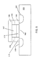
- FIG. 5 illustrates a third embodiment wherein the buffer layers below the ferroelectric regions are made of different materials and have a different thickness than the dielectric between the ferroelectric regions.
- FIG. 6 illustrates a fourth embodiment wherein the top buffer layer is formed between the gate electrode and the top dielectric layer.
- FIG. 7 illustrates a fifth embodiment wherein the top buffer layers are formed over the ferroelectric regions.
- FIG. 8 illustrates an example of the applied voltages to the ferroelectric transistor structure in order to polarize a left ferroelectric region to one state.
- FIG. 9 illustrates an example of a read bias of the ferroelectric FET wherein one n-type region acts as a source.
- FIG. 10 illustrates an example of a bias that polarizes the ferroelectric material in a left region to a “high state”.
- FIG. 11 illustrates an example of a read bias of the ferroelectric FET wherein an n-type region acts as a source when the ferroelectric material of region is polarized in the high state.
- FIG. 12 illustrates an example of the applied voltages to the ferroelectric transistor structure in order to polarize right ferroelectric region to a “low state”.
- FIG. 13 illustrates an example of a read bias of the ferroelectric FET wherein an n-type region acts as a source.
- FIG. 14 illustrates an example of a bias that polarizes the ferroelectric material in a right region to a “high state”.
- FIG. 15 illustrates an example of a read bias of the ferroelectric FET wherein an n-type region acts as a source.
- FIG. 16 is a plan view diagram illustrating the ferroelectric FET structures placed and electrically connected in rows and columns to form a memory array.
- FIG. 17 illustrates another embodiment wherein the ferroelectric material is removed between the word lines.
- FIG. 18 is a schematic diagram illustrating the connection of ferroelectric FETs connected in rows and columns to form a memory array.
- FIG. 19 is a schematic diagram indicating a bias on the columns and rows to polarize the left ferroelectric region of an FET to a low state according to the present invention.
- FIG. 20 is a schematic diagram indicating a bias on the columns and rows to polarize the left ferroelectric region of an FET to a high state according to the present invention.
- FIG. 21 is a schematic diagram indicating a bias on the columns and rows to read the polarized state of the left ferroelectric region of an FET according to the present invention.
- FIG. 22 illustrates the biasing in order to read the polarization of the right ferroelectric region of an FET according to the present invention.
- FIG. 3 is a cross sectional view illustrating the structure of a ferroelectric FET according to one embodiment of the present invention.
- n-type silicon regions 101 and 102 are formed within p-type silicon substrate 100 , the region between them disposing the channel region 103 .
- a dielectric buffer layer 104 is formed on the channel region 103 .
- Ferroelectric regions 105 and 106 are formed on dielectric buffer layer 104 in the vicinity of source 101 and drain 102 , and a non-ferroelectric gate oxide layer 107 is formed between these ferroelectric regions 105 and 106 .
- a gate electrode layer 108 is formed on top of dielectric layer 107 and ferroelectric regions 105 and 106 . In operation, ferroelectric region 105 stores one bit and ferroelectric region 106 stores another bit.
- Ferroelectric regions 105 and 106 can be formed using a sidewall processing technique.
- the non-ferroelectric gate dielectric 107 is deposited on the buffer layer 104 and patterned, followed by a deposition of a ferroelectric layer.
- the ferroelectric layer is then planarized using techniques such as chemical mechanical polishing (CMP), thereby removing the ferroelectric material from the top of non-ferroelectric dielectric gate oxide layer 107 but leaving the ferroelectric material on the sides of dielectric gate oxide 107 layer, forming ferroelectric regions 105 and 106 on the sides of dielectric gate oxide layer 107 .
- CMP chemical mechanical polishing
- the ferroelectric material utilized can be any material exhibiting hysteresis, including ferroelectrics with low dielectric constants and materials having the general formula A x Mn y O z where x, y, z vary from 0.1 to 10 and A is a rare earth selected from a group consisting of Ce, Pr, Nd, Pm, Sm, Eu, GD, Tb, Dy, Ho, Er, Tm, Yb, Lu, Y or Sc.
- Ferroelectric materials with low dielectric constants increase the component of voltage across the ferroelectric layer when a voltage is applied across a structure consisting of buffer dielectric layers and ferroelectric layers.
- Such materials can be produced by any of a variety of methods including sputtering, spin-on gels, and MOCVD (metal-oxide-chemical-vapor-deposition).
- Materials used as the dielectric layer include silicon nitride, silicon dioxide, thermally grown silicon dioxide, and dielectric materials with high dielectric constants. Buffer dielectric materials with high dielectric constants increase the component of voltage across the ferroelectric layer when a voltage is applied across a structure consisting of buffer dielectric layers and ferroelectric layers. More than one material can be layered to form the dielectric layer such as a silicon nitride layer overlying a silicon dioxide layer. Such materials can be formed by any of a variety of methods including ALD (atomic layer deposition), sputtering, and MOCVD.
- ALD atomic layer deposition
- sputtering atomic layer deposition
- MOCVD MOCVD
- Materials used as the electrode layer include metals, doped polysilicon, and metal silicides.
- FIG. 4 illustrates a second embodiment wherein the n-type region of source 101 and 102 partially or fully overlaps ferroelectric regions 106 and 105 , respectively.
- the substrate is a CMOS compatible silicon substrate or a silicon-on-insulator substrate or the like.
- FIG. 5 illustrates a third embodiment wherein buffer layer 118 and 119 under ferroelectric regions 105 and 106 , respectively, are formed with a different material and a different thickness from buffer layer 110 under non-ferroelectric gate oxide 107 .
- FIG. 6 illustrates a fourth embodiment wherein top buffer layer 111 is formed between the gate electrode 108 and the layer consisting of ferroelectric region 105 , gate oxide layer 107 , and ferroelectric region 106 .
- this top buffer layer serves to reduce high electric fields at the gate electrode/ferroelectric interface, to contain the ferroelectric materials within an encapsulated region, to reduce leakage currents, and to keep hydrogen away from the ferroelectric materials.
- FIG. 7 illustrates a fifth embodiment wherein top buffer layers 113 and 112 are formed over ferroelectric regions 105 and 106 , respectively. In this embodiment, no buffer layer is formed between gate electrode layer 108 and the bottom oxide layer 110 .
- FIG. 8 illustrates an example of the voltages applied to the ferroelectric transistor structure in order to polarize left ferroelectric region 106 to one state, herein referred to as the “low state”.
- a voltage of +1.5V is applied to the gate electrode, ⁇ 1.5V is applied to n-type region 101 , 0V is applied to n-type region 102 , and ⁇ 1.5V is applied to substrate 100 , thereby avoiding a forward bias condition between n-type region 101 and substrate 100 .
- the applied voltage between n-type region 101 and electrode 108 determines the electric field strength on ferroelectric region 106
- the applied voltage between n-type region 102 and electrode 108 determines the field strength on ferroelectric region 105 .
- the coercive voltage is assumed to be 2V. Accordingly, the polarization of ferroelectric region 105 remains unchanged since the applied voltage between n-type region 102 and electrode 108 is 1.5V, less than the coercive voltage. The voltage between n-type region 101 and electrode 108 is 3V, greater than the coercive voltage. It is assumed for the purposes of illustration that voltage drops across bottom buffer layer 104 and the top buffer layer, if there is one, are sufficiently small due to appropriate dielectric constants and thicknesses in order to produce at least a coercive voltage across ferroelectric region 106 . Accordingly, ferroelectric region 106 polarizes to a low state.
- ferroelectric polarization When the applied voltages are removed, the ferroelectric polarization remains. Since ferroelectric region 106 is in the vicinity of n-type region 101 , the electric field affects the turn-on threshold voltage when n-type region 101 is operated as the source of the transistor. The direction of the electric field produced when ferroelectric region 106 is polarized to the “low state” causes the turn-on threshold to be lower than if that same region were not polarized. For the purposes of illustration, the threshold voltage corresponding to the low state is 0.5V.
- FIG. 9 illustrates an example of a read bias of the ferroelectric FET wherein n-type region 101 acts as a source.
- a voltage of 1.0V is applied to gate electrode 108 , 0V to n-type region 101 thereby acting as the source, 1.0V to n-type region 102 thereby acting as a drain, and 0V to substrate 100 .
- ferroelectric region 106 is polarized to the low state, the turn-on threshold of the FET is 0.5V.
- the polarization of the ferroelectric material in region 105 does not affect the threshold voltage since the channel is pinched off in this region, and carriers are injected from the point of pinch-off to the depletion region around the drain. Therefore a current flows from source 101 to drain 102 in this device.
- FIG. 10 illustrates an example of a bias that polarizes the ferroelectric material in region 106 to a “high state”.
- a voltage of ⁇ 1.5V is applied to the gate electrode, +1.5V is applied to n-type region 101 , 0V is applied to n-type region 102 , and 0V is applied to substrate 100 .
- the applied voltage between n-type region 101 and electrode 108 is higher than the coercive voltage, and the electric field is in the direction to polarize the ferroelectric material to a “high state”.
- the threshold voltage corresponding to the high state is 1.5V.
- FIG. 11 illustrates an example of a read bias of the ferroelectric FET wherein n-type region 101 acts as a source when the ferroelectric material of region 106 is polarized in the high state.
- a voltage of 1.0V is applied to gate electrode 108 , 0V to n-type region 101 thereby acting as the source, 1.0V to n-type region 102 thereby acting as a drain, and 0V to substrate 100 .
- the turn-on threshold of the FET is 1.5V.
- the polarization of the ferroelectric material in region 105 does not affect the threshold voltage since the channel in this region is depleted. Since the turn-on threshold voltage is higher than the gate-to-source voltage, no current flows through this device.
- FIG. 12 illustrates an example of the voltages applied to the ferroelectric transistor structure in order to polarize right ferroelectric region 105 to the “low state”.
- a voltage of +1.5V is applied to the gate electrode, 0V is applied to n-type region 101 , ⁇ 1.5V is applied to n-type region 102 , and ⁇ 1.5V is applied to substrate 100 , thereby avoiding a forward bias condition between n-type region 102 and substrate 100 .
- the applied voltage between n-type region 102 and electrode 108 is greater than the coercive voltage, while the voltage between n-type region 101 and gate electrode 108 is less than the coercive voltage.
- ferroelectric region 106 remains unchanged since the applied voltage between n-type region 101 and electrode 108 is 1.5V, less than the coercive voltage.
- the voltage between n-type region 102 and electrode 108 is 3V, greater than the coercive voltage. It is assumed for the purposes of illustration that voltage drops across bottom buffer layer 104 and the top buffer layer 108 , if there is one, are sufficiently small to allow at least a coercive voltage across ferroelectric region 105 . Accordingly, ferroelectric region 105 is polarized to the low state.
- FIG. 13 illustrates an example of a read bias of the ferroelectric FET wherein n-type region 102 acts as a source.
- a voltage of 1.0V is applied to gate electrode 108 , 0V to n-type region 102 thereby acting as the source, 1.0V to n-type region 101 thereby acting as a drain, and 0V to substrate 100 .
- ferroelectric region 105 is polarized to the low state
- the turn-on threshold of the FET is 0.5V.
- the polarization of the ferroelectric material in region 106 does not affect the threshold voltage since the channel in this region is depleted. Therefore a current flows from source 102 to drain 101 in this device.
- FIG. 14 illustrates an example of a bias that polarizes the ferroelectric material in region 105 to a high state.
- a voltage of ⁇ 1.5V is applied to the gate electrode, 0V is applied to n-type region 101 , +1.5V is applied to n-type region 102 , and 0V is applied to substrate 100 .
- the applied voltage between n-type region 102 and electrode 108 is higher than the coercive voltage; the electric field is the direction to polarize the ferroelectric material to a high state, corresponding to a turn-on threshold of 1.5V.
- FIG. 15 illustrates an example of a read bias of the ferroelectric FET wherein n-type region 102 acts as a source and the ferroelectric region 105 is polarized to the high state.
- a voltage of 1.0V is applied to gate electrode 108 , 0V to n-type region 102 thereby acting as the source, 1.0V to n-type region 101 thereby acting as a drain, and 0V to substrate 100 .
- the turn-on threshold of the FET is 1.5V.
- the polarization of the ferroelectric material in region 106 does not affect the threshold voltage since the channel in this region is depleted. Therefore, no current flows between source 102 to drain 101 in this device.
- the voltages used to polarize the ferroelectric regions 105 and 106 can be made significantly larger in magnitude than the voltages used to read the data state.
- the voltages used to polarize the ferroelectric material might be 5V, while the peak read voltages used are 1V. Successive voltages applied to the device during the read, though less than the coercive voltage, nevertheless may alter the polarization of some ferroelectric materials. By using voltages for read that are low relative to the polarization voltage, potential disturbs to the polarization state that might result are minimized.
- FIG. 16 is a plan view diagram illustrating the ferroelectric FET structures placed and electrically connected in rows and columns to form a memory array.
- Gate electrodes of FETs in any given row of the array are connected with a word line.
- the word line consists of a strip of conductive thin film 140 or 141 across the array, consisting of any conductive material including platinum, aluminum, polysilicon, and silicides.
- the source and drains of FETs in any given column of the array are electrically connected.
- sources of FETs in a given column are connected with strips of n-type material formed in a p-type substrate, such as diffused bit line 122 of FIG. 16 . Drains are similarly connected with diffused bit line 123 .
- the ferroelectric material is formed on the inside edges of the word line where the bit line intersects the word line.
- ferroelectric material 133 and 134 are formed along the inside edge of bit line 122 and 123 , respectively. This ferroelectric material may overlap, partially overlap, or underlap the diffused bit line.
- the region 150 of FIG. 16 is a single cell within the memory array, each terminal marked with the same numbers as used in the cross sectional diagram of FIG. 15 .
- Bit line 122 and bit line 123 under word line 140 form n-type region source/drain 101 and source/drain 102 , respectively.
- the region between source/drain 101 and 102 disposes the channel region 103 .
- Above channel 103 is the gate electrode 108 .
- Ferroelectric regions 105 and 106 in the memory cell are formed where bit line 122 and 123 intersect word line 140 , respectively.
- FIG. 17 illustrates another embodiment wherein the ferroelectric material is not removed between the word lines.
- the ferroelectric material without an overlying word line is electrically inactive since the ferroelectric material in those areas has no top electrode.
- FIG. 18 is a schematic diagram illustrating the connection of ferroelectric FETs connected in rows and columns to form a memory array.
- the diagram shows word line 140 connecting the gates of FETs 160 and 161 , and word line 141 connecting the gates of FETs 162 and 163 .
- Columns 120 and 121 connects the sources and drains of FETs 160 and 162 .
- Columns 122 and 123 connect the sources and drains of FETs 161 and 163 .
- FIG. 19 is a schematic diagram indicating a bias on the columns and rows to polarize the left ferroelectric region of FET 161 to a low state.
- a voltage of ⁇ 1.5V is applied to the selected bit line 122 , and +1.5V on selected word line 140 .
- a voltage of ⁇ 1.5V is applied to the substrate to avoid the n-type regions forward biasing to the substrate. More than a coercive voltage is thereby applied across left ferroelectric region of FET 161 , polarizing it to a low state.
- 0V is applied to unselected word lines and bit lines, thereby applying less than a coercive voltage to right ferroelectric region of FET 161 , and so this polarization stays unchanged.
- FET 163 illustrates that less than a coercive voltage is also applied to an FET on a deselected word line but selected bit line.
- FET 162 is an example of an FET bias on a deselected word line and deselected bit lines. In this case, no electric field is applied across the ferroelectric regions of the device, thereby leaving the polarization unchanged.
- FIG. 20 is a schematic diagram indicating a bias on the columns and rows to polarize the left ferroelectric region of FET 161 to a high state.
- a voltage of +1.5V is applied to the selected bit line 122 , and ⁇ 1.5V on selected word line 140 .
- the substrate is biased to 0V. More than a coercive voltage is thereby applied across left ferroelectric region of FET 161 , polarizing it to a high state.
- 0V is applied to unselected word lines and bit lines, thereby applying less than a coercive voltage to right ferroelectric region of FET 161 , and so this polarization stays unchanged.
- FET 163 illustrates that less than a coercive voltage is also applied to an FET on a deselected word line but selected bit line.
- FET 162 is an example of an FET bias on a deselected word line and deselected bit lines. In this case, no electric field is applied across the ferroelectric regions of the device, thereby leaving the polarization unchanged.
- FIG. 21 is a schematic diagram indicating a bias on the columns and rows to read the polarized state of left ferroelectric region of FET 161 .
- a voltage of +1.0V is applied to selected word line 140 .
- 0V is applied to the bit line connected to the left n-type region of FET 161 , that n-type region thereby acting as the source.
- the gate-to-source voltage is therefore 1.0V.
- 1.0V is applied to the other n-type region of FET 161 , thereby acting as the drain. If the high state is stored on the left ferroelectric, FET 161 remains off since the turn-on threshold of FET 161 would then be 1.5V, higher than the applied gate-to-source voltage. If a low state is stored in the left ferroelectric, FET 161 turns on since the turn-on threshold of the FET is 0.5V, less than the gate-to-source voltage.
- the FETs along the selected word line such as FET 160 , have 0V on both the source and drain.
- the FETs along the unselected word line, such as FETs 162 and 163 have 0V on the gate.
- FIG. 22 illustrates the biasing in order to read the polarization of the right ferroelectric region of FET 161 .
- Biasing is identical to FIG. 21, except that the voltages on bit line 122 and 123 are reversed.
- the right n-type region acts as source of FET 161 . Measuring the resulting current determines the polarization state, high current corresponding to a low state and low current corresponding to a high state.
Abstract
Description
Claims (6)
Priority Applications (5)
| Application Number | Priority Date | Filing Date | Title |
|---|---|---|---|
| US10/246,975 US6714435B1 (en) | 2002-09-19 | 2002-09-19 | Ferroelectric transistor for storing two data bits |
| US10/305,205 US6888736B2 (en) | 2002-09-19 | 2002-11-26 | Ferroelectric transistor for storing two data bits |
| AU2003273228A AU2003273228A1 (en) | 2002-09-19 | 2003-08-04 | Ferroelectric transistor for storing two data bits |
| PCT/US2003/024385 WO2004027821A2 (en) | 2002-09-19 | 2003-08-04 | Ferroelectric transistor for storing two data bits |
| US10/752,245 US7034349B2 (en) | 2002-09-19 | 2004-01-06 | Ferroelectric transistor for storing two data bits |
Applications Claiming Priority (1)
| Application Number | Priority Date | Filing Date | Title |
|---|---|---|---|
| US10/246,975 US6714435B1 (en) | 2002-09-19 | 2002-09-19 | Ferroelectric transistor for storing two data bits |
Related Child Applications (2)
| Application Number | Title | Priority Date | Filing Date |
|---|---|---|---|
| US10/305,205 Continuation-In-Part US6888736B2 (en) | 2002-09-19 | 2002-11-26 | Ferroelectric transistor for storing two data bits |
| US10/752,245 Division US7034349B2 (en) | 2002-09-19 | 2004-01-06 | Ferroelectric transistor for storing two data bits |
Publications (2)
| Publication Number | Publication Date |
|---|---|
| US20040057274A1 US20040057274A1 (en) | 2004-03-25 |
| US6714435B1 true US6714435B1 (en) | 2004-03-30 |
Family
ID=31992407
Family Applications (2)
| Application Number | Title | Priority Date | Filing Date |
|---|---|---|---|
| US10/246,975 Expired - Fee Related US6714435B1 (en) | 2002-09-19 | 2002-09-19 | Ferroelectric transistor for storing two data bits |
| US10/752,245 Expired - Fee Related US7034349B2 (en) | 2002-09-19 | 2004-01-06 | Ferroelectric transistor for storing two data bits |
Family Applications After (1)
| Application Number | Title | Priority Date | Filing Date |
|---|---|---|---|
| US10/752,245 Expired - Fee Related US7034349B2 (en) | 2002-09-19 | 2004-01-06 | Ferroelectric transistor for storing two data bits |
Country Status (1)
| Country | Link |
|---|---|
| US (2) | US6714435B1 (en) |
Cited By (19)
| Publication number | Priority date | Publication date | Assignee | Title |
|---|---|---|---|---|
| US20040106261A1 (en) * | 2002-12-03 | 2004-06-03 | Asm International N.V. | Method of forming an electrode with adjusted work function |
| US20040106249A1 (en) * | 2002-12-03 | 2004-06-03 | Hannu Huotari | Method to fabricate dual metal CMOS devices |
| US20040104439A1 (en) * | 2002-12-03 | 2004-06-03 | Asm International N.V. | Method of depositing barrier layer from metal gates |
| US20060068508A1 (en) * | 2004-09-28 | 2006-03-30 | Sharp Laboratories Of America, Inc. | Method for operating an MFIS ferroelectric memory array |
| US20060081901A1 (en) * | 2004-09-10 | 2006-04-20 | Fujitsu Limted | Ferroelectric memory, multivalent data recording method and multivalent data reading method |
| US20070097762A1 (en) * | 2003-05-20 | 2007-05-03 | Yoshifumi Yaoi | Semiconductor storage device, redundancy circuit thereof, and portable electronic device |
| US20080085610A1 (en) * | 2006-10-05 | 2008-04-10 | Asm America, Inc. | Ald of metal silicate films |
| US20080158934A1 (en) * | 2006-12-27 | 2008-07-03 | Hynix Semiconductor, Inc. | Semiconductor Memory Device With Ferroelectric Device And Refresh Method Thereof |
| US7563715B2 (en) | 2005-12-05 | 2009-07-21 | Asm International N.V. | Method of producing thin films |
| US20090214767A1 (en) * | 2001-03-06 | 2009-08-27 | Asm America, Inc. | Doping with ald technology |
| KR100919558B1 (en) * | 2006-12-27 | 2009-10-01 | 주식회사 하이닉스반도체 | Semiconductor memory device using ferroelectric device and method for refresh thereof |
| KR100919584B1 (en) * | 2006-12-27 | 2009-10-01 | 주식회사 하이닉스반도체 | Semiconductor memory device using ferroelectric device and method for refresh thereof |
| US20100193955A1 (en) * | 2009-02-02 | 2010-08-05 | Asm America, Inc. | Plasma-enhanced atomic layer deposition of conductive material over dielectric layers |
| US8945675B2 (en) | 2008-05-29 | 2015-02-03 | Asm International N.V. | Methods for forming conductive titanium oxide thin films |
| US20150070964A1 (en) * | 2013-09-11 | 2015-03-12 | Kabushiki Kaisha Toshiba | Semiconductor memory device and method of operating the same |
| US9523148B1 (en) | 2015-08-25 | 2016-12-20 | Asm Ip Holdings B.V. | Process for deposition of titanium oxynitride for use in integrated circuit fabrication |
| US9540729B1 (en) | 2015-08-25 | 2017-01-10 | Asm Ip Holding B.V. | Deposition of titanium nanolaminates for use in integrated circuit fabrication |
| US10510862B2 (en) | 2018-03-23 | 2019-12-17 | Toshiba Memory Corporation | Semiconductor memory device |
| US20190392758A1 (en) * | 2018-06-21 | 2019-12-26 | Samsung Display Co., Ltd. | Display device |
Families Citing this family (17)
| Publication number | Priority date | Publication date | Assignee | Title |
|---|---|---|---|---|
| TWI451570B (en) * | 2011-11-15 | 2014-09-01 | Univ Nat Chiao Tung | Multi-bit resistive switching memory cell and array |
| US8796751B2 (en) * | 2012-11-20 | 2014-08-05 | Micron Technology, Inc. | Transistors, memory cells and semiconductor constructions |
| TWI485706B (en) * | 2013-02-07 | 2015-05-21 | Winbond Electronics Corp | Resistive memory and memory cell thereof |
| CN105493265B (en) * | 2013-07-25 | 2018-10-16 | 独立行政法人产业技术综合研究所 | Strong dielectric body device and its manufacturing method |
| US9558804B2 (en) * | 2014-07-23 | 2017-01-31 | Namlab Ggmbh | Charge storage ferroelectric memory hybrid and erase scheme |
| US10056393B2 (en) * | 2016-03-01 | 2018-08-21 | Namlab Ggmbh | Application of antiferroelectric like materials in non-volatile memory devices |
| JP6751866B2 (en) | 2016-04-22 | 2020-09-09 | 国立研究開発法人産業技術総合研究所 | Manufacturing method of semiconductor ferroelectric storage element and semiconductor ferroelectric storage transistor |
| KR20180106662A (en) * | 2017-03-21 | 2018-10-01 | 에스케이하이닉스 주식회사 | Ferroelectric Memory Device |
| WO2019066875A1 (en) * | 2017-09-28 | 2019-04-04 | Intel Corporation | Field effect transistors having ferroelectric or antiferroelectric gate dielectric structure |
| US10504576B2 (en) | 2017-12-19 | 2019-12-10 | Micron Technology, Inc. | Current separation for memory sensing |
| KR102494684B1 (en) * | 2018-05-10 | 2023-02-02 | 에스케이하이닉스 주식회사 | Ferroelectric Semiconductor Device and Method of Manufacturing the same |
| CN109801977A (en) * | 2019-01-28 | 2019-05-24 | 中国科学院微电子研究所 | Memory |
| WO2020154843A1 (en) * | 2019-01-28 | 2020-08-06 | 中国科学院微电子研究所 | Fusion memory |
| US11158361B2 (en) * | 2019-07-05 | 2021-10-26 | Ferroelectric Memory Gmbh | Memory cell arrangement and methods thereof |
| DE102021105038A1 (en) | 2020-05-29 | 2021-12-02 | Taiwan Semiconductor Manufacturing Co., Ltd. | MULTI-BIT STORAGE DEVICE AND METHOD OF OPERATING THE SAME |
| US11532746B2 (en) * | 2020-05-29 | 2022-12-20 | Taiwan Semiconductor Manufacturing Company, Ltd. | Multi-bit memory storage device and method of operating same |
| CN115064555B (en) * | 2022-06-09 | 2023-04-07 | 西安电子科技大学 | Multi-value memory device of ferroelectric assembled grid field effect transistor |
Citations (95)
| Publication number | Priority date | Publication date | Assignee | Title |
|---|---|---|---|---|
| US3832700A (en) | 1973-04-24 | 1974-08-27 | Westinghouse Electric Corp | Ferroelectric memory device |
| US4860254A (en) | 1986-01-31 | 1989-08-22 | Bayer Aktiengesellschaft | Non-volatile electronic memory |
| US5046043A (en) | 1987-10-08 | 1991-09-03 | National Semiconductor Corporation | Ferroelectric capacitor and memory cell including barrier and isolation layers |
| US5060191A (en) | 1988-07-08 | 1991-10-22 | Olympus Optical Co., Ltd. | Ferroelectric memory |
| US5070385A (en) | 1989-10-20 | 1991-12-03 | Radiant Technologies | Ferroelectric non-volatile variable resistive element |
| US5146299A (en) | 1990-03-02 | 1992-09-08 | Westinghouse Electric Corp. | Ferroelectric thin film material, method of deposition, and devices using same |
| US5198994A (en) | 1988-08-31 | 1993-03-30 | Kabushiki Kaisha Toshiba | Ferroelectric memory device |
| US5227855A (en) | 1990-01-24 | 1993-07-13 | Kabushiki Kaisha Toshiba | Semiconductor memory device having a ferroelectric substance as a memory element |
| US5302842A (en) | 1992-07-20 | 1994-04-12 | Bell Communications Research, Inc. | Field-effect transistor formed over gate electrode |
| US5307305A (en) | 1991-12-04 | 1994-04-26 | Rohm Co., Ltd. | Semiconductor device having field effect transistor using ferroelectric film as gate insulation film |
| US5345414A (en) | 1992-01-27 | 1994-09-06 | Rohm Co., Ltd. | Semiconductor memory device having ferroelectric film |
| US5365094A (en) | 1991-11-18 | 1994-11-15 | Rohm Company Limited | Semiconductor device including ferroelectric nonvolatile memory |
| US5378905A (en) | 1992-02-24 | 1995-01-03 | Rohm Co., Ltd. | Ferroelectric field effect transistor with fluoride buffer and IV-VI ferroelectric |
| US5384729A (en) | 1991-10-28 | 1995-01-24 | Rohm Co., Ltd. | Semiconductor storage device having ferroelectric film |
| US5418389A (en) | 1992-11-09 | 1995-05-23 | Mitsubishi Chemical Corporation | Field-effect transistor with perovskite oxide channel |
| US5434811A (en) | 1987-11-19 | 1995-07-18 | National Semiconductor Corporation | Non-destructive read ferroelectric based memory circuit |
| US5479317A (en) | 1994-10-05 | 1995-12-26 | Bell Communications Research, Inc. | Ferroelectric capacitor heterostructure and method of making same |
| US5515311A (en) | 1993-07-26 | 1996-05-07 | Olympus Optical Co., Ltd. | Method of driving ferroelectric memory |
| US5519235A (en) | 1994-11-18 | 1996-05-21 | Bell Communications Research, Inc. | Polycrystalline ferroelectric capacitor heterostructure employing hybrid electrodes |
| US5523964A (en) | 1994-04-07 | 1996-06-04 | Symetrix Corporation | Ferroelectric non-volatile memory unit |
| US5541870A (en) | 1994-10-28 | 1996-07-30 | Symetrix Corporation | Ferroelectric memory and non-volatile memory cell for same |
| US5541873A (en) | 1994-06-16 | 1996-07-30 | Rohm Co., Ltd. | Nonvolatile memory |
| US5541871A (en) | 1994-01-18 | 1996-07-30 | Rohm Co., Ltd. | Nonvolatile ferroelectric-semiconductor memory |
| US5563081A (en) | 1992-03-23 | 1996-10-08 | Rohm Co., Inc. | Method for making a nonvolatile memory device utilizing a field effect transistor having a ferroelectric gate film |
| US5578846A (en) | 1995-03-17 | 1996-11-26 | Evans, Jr.; Joseph T. | Static ferroelectric memory transistor having improved data retention |
| US5621681A (en) | 1995-03-22 | 1997-04-15 | Samsung Electronics Co., Ltd. | Device and manufacturing method for a ferroelectric memory |
| US5623439A (en) | 1994-06-01 | 1997-04-22 | Fujitsu Limited | Ferroelectric memory device |
| US5640030A (en) * | 1995-05-05 | 1997-06-17 | International Business Machines Corporation | Double dense ferroelectric capacitor cell memory |
| US5736759A (en) | 1996-07-24 | 1998-04-07 | Nec Research Institute, Inc. | Reduced fatigue ferroelectric element |
| US5739563A (en) | 1995-03-15 | 1998-04-14 | Kabushiki Kaisha Toshiba | Ferroelectric type semiconductor device having a barium titanate type dielectric film and method for manufacturing the same |
| US5757042A (en) | 1996-06-14 | 1998-05-26 | Radiant Technologies, Inc. | High density ferroelectric memory with increased channel modulation and double word ferroelectric memory cell for constructing the same |
| US5768185A (en) | 1993-12-28 | 1998-06-16 | Rohm Co., Ltd. | Non-volatile semiconductor memory of a metal ferroelectric field effect transistor |
| US5780886A (en) | 1996-05-30 | 1998-07-14 | Oki Electric Industry Co., Ltd. | Non-volatile semiconductor memory cell and method for production thereof |
| US5789775A (en) | 1996-01-26 | 1998-08-04 | Radiant Technologies | High density memory and double word ferroelectric memory cell for constructing the same |
| US5808676A (en) | 1995-01-03 | 1998-09-15 | Xerox Corporation | Pixel cells having integrated analog memories and arrays thereof |
| US5822239A (en) | 1996-08-20 | 1998-10-13 | Tokyo Institute Of Technology | Method of writing data to a single transistor type ferroelectric memory |
| US5825317A (en) | 1997-04-07 | 1998-10-20 | Motorola, Inc. | Digital-to-analog converter and method of calibrating |
| US5858533A (en) | 1993-10-15 | 1999-01-12 | Abb Research Ltd. | Composite material |
| US5872739A (en) | 1997-04-17 | 1999-02-16 | Radiant Technologies | Sense amplifier for low read-voltage memory cells |
| US5877977A (en) | 1996-09-10 | 1999-03-02 | National Semiconductor Corporation | Nonvolatile memory based on metal-ferroelectric-metal-insulator semiconductor structure |
| US5887117A (en) | 1997-01-02 | 1999-03-23 | Sharp Kabushiki Kaisha | Flash evaporator |
| US5886920A (en) | 1997-12-01 | 1999-03-23 | Motorola, Inc. | Variable conducting element and method of programming |
| US5919515A (en) | 1995-08-25 | 1999-07-06 | Tdk Corporation | Ferroelectric thin film, electric device and method for preparing ferroelectric thin film |
| US5946224A (en) | 1996-12-27 | 1999-08-31 | Rohm Co., Ltd. | Ferroelectric memory device, a method for read out stored data and a method for standing-by |
| US5959879A (en) | 1997-06-09 | 1999-09-28 | Samsung Electronics Co., Ltd. | Ferroelectric memory devices having well region word lines and methods of operating same |
| US5962884A (en) | 1997-03-07 | 1999-10-05 | Sharp Laboratories Of America, Inc. | Single transistor ferroelectric memory cell with asymmetrical ferroelectric polarization and method of making the same |
| US5977577A (en) | 1994-11-15 | 1999-11-02 | Radiant Technologies, Inc | Ferroelectric based memory devices utilizing low curie point ferroelectrics and encapsulation |
| US5998819A (en) | 1996-03-19 | 1999-12-07 | Sharp Kabushiki Kaisha | Thin ferroelectric film element having a multi-layered thin ferroelectric film and method for manufacturing the same |
| US6025735A (en) | 1996-12-23 | 2000-02-15 | Motorola, Inc. | Programmable switch matrix and method of programming |
| US6027947A (en) | 1996-08-20 | 2000-02-22 | Ramtron International Corporation | Partially or completely encapsulated top electrode of a ferroelectric capacitor |
| US6031754A (en) | 1998-11-02 | 2000-02-29 | Celis Semiconductor Corporation | Ferroelectric memory with increased switching voltage |
| US6067244A (en) | 1997-10-14 | 2000-05-23 | Yale University | Ferroelectric dynamic random access memory |
| US6066868A (en) | 1999-03-31 | 2000-05-23 | Radiant Technologies, Inc. | Ferroelectric based memory devices utilizing hydrogen barriers and getters |
| US6069381A (en) | 1997-09-15 | 2000-05-30 | International Business Machines Corporation | Ferroelectric memory transistor with resistively coupled floating gate |
| US6087688A (en) | 1998-03-03 | 2000-07-11 | Fuji Electric Co., Ltd. | Field effect transistor |
| US6091621A (en) | 1997-12-05 | 2000-07-18 | Motorola, Inc. | Non-volatile multistate memory cell using a ferroelectric gate fet |
| US6104049A (en) | 1997-03-03 | 2000-08-15 | Symetrix Corporation | Ferroelectric memory with ferroelectric thin film having thickness of 90 nanometers or less, and method of making same |
| US6121648A (en) | 1999-03-31 | 2000-09-19 | Radiant Technologies, Inc | Ferroelectric based memory devices utilizing hydrogen getters and recovery annealing |
| US6130103A (en) | 1998-04-17 | 2000-10-10 | Symetrix Corporation | Method for fabricating ferroelectric integrated circuits |
| US6140672A (en) | 1999-03-05 | 2000-10-31 | Symetrix Corporation | Ferroelectric field effect transistor having a gate electrode being electrically connected to the bottom electrode of a ferroelectric capacitor |
| US6144579A (en) | 1997-12-09 | 2000-11-07 | Fujitsu Limited | Ferroelectric memory device |
| US6147895A (en) | 1999-06-04 | 2000-11-14 | Celis Semiconductor Corporation | Ferroelectric memory with two ferroelectric capacitors in memory cell and method of operating same |
| US6151241A (en) | 1999-05-19 | 2000-11-21 | Symetrix Corporation | Ferroelectric memory with disturb protection |
| US6151242A (en) | 1998-06-30 | 2000-11-21 | Kabushiki Kaisha Toshiba | Semiconductor memory device |
| US6165802A (en) | 1998-04-17 | 2000-12-26 | Symetrix Corporation | Method of fabricating ferroelectric integrated circuit using oxygen to inhibit and repair hydrogen degradation |
| US6171934B1 (en) | 1998-08-31 | 2001-01-09 | Symetrix Corporation | Recovery of electronic properties in process-damaged ferroelectrics by voltage-cycling |
| US6194751B1 (en) | 1994-11-15 | 2001-02-27 | Radiant Technologies, Inc | Ferroelectric based memory devices utilizing low Curie point ferroelectrics and encapsulation |
| US6201731B1 (en) | 1999-05-28 | 2001-03-13 | Celis Semiconductor Corporation | Electronic memory with disturb prevention function |
| US6207465B1 (en) | 1998-04-17 | 2001-03-27 | Symetrix Corporation | Method of fabricating ferroelectric integrated circuit using dry and wet etching |
| US6225156B1 (en) | 1998-04-17 | 2001-05-01 | Symetrix Corporation | Ferroelectric integrated circuit having low sensitivity to hydrogen exposure and method for fabricating same |
| US6225656B1 (en) | 1998-12-01 | 2001-05-01 | Symetrix Corporation | Ferroelectric integrated circuit with protective layer incorporating oxygen and method for fabricating same |
| US6236076B1 (en) | 1999-04-29 | 2001-05-22 | Symetrix Corporation | Ferroelectric field effect transistors for nonvolatile memory applications having functional gradient material |
| US6245580B1 (en) | 1999-01-11 | 2001-06-12 | Symetrix Corporation | Low temperature process for fabricating layered superlattice materials and making electronic devices including same |
| US6246602B1 (en) | 1996-12-27 | 2001-06-12 | Rohm Co., Ltd. | Ferroelectric storage device |
| US6245451B1 (en) | 1996-09-27 | 2001-06-12 | Rohm Co., Ltd. | Ferroelectric material, method of manufacturing the same, semiconductor memory, and method of manufacturing the same |
| US6256220B1 (en) | 1997-09-15 | 2001-07-03 | Celis Semiconductor Corporation | Ferroelectric memory with shunted isolated nodes |
| US6255121B1 (en) | 1999-02-26 | 2001-07-03 | Symetrix Corporation | Method for fabricating ferroelectric field effect transistor having an interface insulator layer formed by a liquid precursor |
| US6285577B1 (en) | 1999-09-30 | 2001-09-04 | Rohm Co., Ltd. | Non-volatile memory using ferroelectric capacitor |
| US6307225B1 (en) | 1997-12-19 | 2001-10-23 | Sharp Kabushiki Kaisha | Insulating material, substrate covered with an insulating film, method of producing the same, and thin-film device |
| US6310373B1 (en) | 1992-10-23 | 2001-10-30 | Symetrix Corporation | Metal insulator semiconductor structure with polarization-compatible buffer layer |
| US6319542B1 (en) | 1993-03-31 | 2001-11-20 | Texas Instruments Incorporated | Lightly donor doped electrodes for high-dielectric-constant materials |
| US6322849B2 (en) | 1998-11-13 | 2001-11-27 | Symetrix Corporation | Recovery of electronic properties in hydrogen-damaged ferroelectrics by low-temperature annealing in an inert gas |
| US6326315B1 (en) | 2000-03-09 | 2001-12-04 | Symetrix Corporation | Low temperature rapid ramping anneal method for fabricating layered superlattice materials and making electronic devices including same |
| US6335550B1 (en) | 1999-02-26 | 2002-01-01 | Sharp Kabushiki Kaisha | Fet with ferroelectric gate |
| US6339238B1 (en) | 1998-10-13 | 2002-01-15 | Symetrix Corporation | Ferroelectric field effect transistor, memory utilizing same, and method of operating same |
| US6358758B2 (en) | 1998-10-13 | 2002-03-19 | Symetrix Corporation | Low imprint ferroelectric material for long retention memory and method of making the same |
| US6362068B1 (en) | 1993-03-31 | 2002-03-26 | Texas Instruments Incorporated | Electrode interface for high-dielectric-constant materials |
| US6365927B1 (en) | 2000-04-03 | 2002-04-02 | Symetrix Corporation | Ferroelectric integrated circuit having hydrogen barrier layer |
| US6370056B1 (en) | 2000-03-10 | 2002-04-09 | Symetrix Corporation | Ferroelectric memory and method of operating same |
| US6372518B1 (en) | 2000-01-26 | 2002-04-16 | Matsushita Electric Industrial Co., Ltd. | Method using unreactive gas anneal and low temperature pretreatment for fabricating layered superlattice materials and making electronic devices including same |
| US6373743B1 (en) | 1999-08-30 | 2002-04-16 | Symetrix Corporation | Ferroelectric memory and method of operating same |
| US6396095B1 (en) | 1999-10-29 | 2002-05-28 | Matsushita Electric Industrial Co., Ltd. | Semiconductor memory and method of driving semiconductor memory |
| US6396093B1 (en) | 1997-11-14 | 2002-05-28 | Rohm Co., Ltd. | Ferroelectric memory with reduced capacitance of ferroelectric gate layer |
| US20020083959A1 (en) | 1999-01-27 | 2002-07-04 | Kiyoyuki Morita | Method for removing foreign matter, method for forming film, semiconductor device and film forming apparatus |
| US6438019B2 (en) * | 1998-07-08 | 2002-08-20 | Infineon Technologies Ag | Ferroelectric random access memory (FeRAM) having storage capacitors with different coercive voltages |
Family Cites Families (4)
| Publication number | Priority date | Publication date | Assignee | Title |
|---|---|---|---|---|
| US165802A (en) * | 1875-07-20 | Improvement in manufacture of chlorine | ||
| JPH07327277A (en) * | 1994-05-31 | 1995-12-12 | Sony Corp | Electronic equipment device and connector for connection |
| US6438031B1 (en) * | 2000-02-16 | 2002-08-20 | Advanced Micro Devices, Inc. | Method of programming a non-volatile memory cell using a substrate bias |
| US6442074B1 (en) * | 2001-02-28 | 2002-08-27 | Advanced Micro Devices, Inc. | Tailored erase method using higher program VT and higher negative gate erase |
-
2002
- 2002-09-19 US US10/246,975 patent/US6714435B1/en not_active Expired - Fee Related
-
2004
- 2004-01-06 US US10/752,245 patent/US7034349B2/en not_active Expired - Fee Related
Patent Citations (103)
| Publication number | Priority date | Publication date | Assignee | Title |
|---|---|---|---|---|
| US3832700A (en) | 1973-04-24 | 1974-08-27 | Westinghouse Electric Corp | Ferroelectric memory device |
| US4860254A (en) | 1986-01-31 | 1989-08-22 | Bayer Aktiengesellschaft | Non-volatile electronic memory |
| US5046043A (en) | 1987-10-08 | 1991-09-03 | National Semiconductor Corporation | Ferroelectric capacitor and memory cell including barrier and isolation layers |
| US5536672A (en) | 1987-10-08 | 1996-07-16 | National Semiconductor Corporation | Fabrication of ferroelectric capacitor and memory cell |
| US5434811A (en) | 1987-11-19 | 1995-07-18 | National Semiconductor Corporation | Non-destructive read ferroelectric based memory circuit |
| US5060191A (en) | 1988-07-08 | 1991-10-22 | Olympus Optical Co., Ltd. | Ferroelectric memory |
| US5198994A (en) | 1988-08-31 | 1993-03-30 | Kabushiki Kaisha Toshiba | Ferroelectric memory device |
| US5070385A (en) | 1989-10-20 | 1991-12-03 | Radiant Technologies | Ferroelectric non-volatile variable resistive element |
| US5227855A (en) | 1990-01-24 | 1993-07-13 | Kabushiki Kaisha Toshiba | Semiconductor memory device having a ferroelectric substance as a memory element |
| US5146299A (en) | 1990-03-02 | 1992-09-08 | Westinghouse Electric Corp. | Ferroelectric thin film material, method of deposition, and devices using same |
| US5384729A (en) | 1991-10-28 | 1995-01-24 | Rohm Co., Ltd. | Semiconductor storage device having ferroelectric film |
| US5365094A (en) | 1991-11-18 | 1994-11-15 | Rohm Company Limited | Semiconductor device including ferroelectric nonvolatile memory |
| US5307305A (en) | 1991-12-04 | 1994-04-26 | Rohm Co., Ltd. | Semiconductor device having field effect transistor using ferroelectric film as gate insulation film |
| US5345414A (en) | 1992-01-27 | 1994-09-06 | Rohm Co., Ltd. | Semiconductor memory device having ferroelectric film |
| US5378905A (en) | 1992-02-24 | 1995-01-03 | Rohm Co., Ltd. | Ferroelectric field effect transistor with fluoride buffer and IV-VI ferroelectric |
| US5563081A (en) | 1992-03-23 | 1996-10-08 | Rohm Co., Inc. | Method for making a nonvolatile memory device utilizing a field effect transistor having a ferroelectric gate film |
| US5302842A (en) | 1992-07-20 | 1994-04-12 | Bell Communications Research, Inc. | Field-effect transistor formed over gate electrode |
| US6310373B1 (en) | 1992-10-23 | 2001-10-30 | Symetrix Corporation | Metal insulator semiconductor structure with polarization-compatible buffer layer |
| US5418389A (en) | 1992-11-09 | 1995-05-23 | Mitsubishi Chemical Corporation | Field-effect transistor with perovskite oxide channel |
| US6319542B1 (en) | 1993-03-31 | 2001-11-20 | Texas Instruments Incorporated | Lightly donor doped electrodes for high-dielectric-constant materials |
| US6362068B1 (en) | 1993-03-31 | 2002-03-26 | Texas Instruments Incorporated | Electrode interface for high-dielectric-constant materials |
| US5515311A (en) | 1993-07-26 | 1996-05-07 | Olympus Optical Co., Ltd. | Method of driving ferroelectric memory |
| US5858533A (en) | 1993-10-15 | 1999-01-12 | Abb Research Ltd. | Composite material |
| US5768185A (en) | 1993-12-28 | 1998-06-16 | Rohm Co., Ltd. | Non-volatile semiconductor memory of a metal ferroelectric field effect transistor |
| US5541871A (en) | 1994-01-18 | 1996-07-30 | Rohm Co., Ltd. | Nonvolatile ferroelectric-semiconductor memory |
| US5523964A (en) | 1994-04-07 | 1996-06-04 | Symetrix Corporation | Ferroelectric non-volatile memory unit |
| US5559733A (en) | 1994-04-07 | 1996-09-24 | Symetrix Corporation | Memory with ferroelectric capacitor connectable to transistor gate |
| US5623439A (en) | 1994-06-01 | 1997-04-22 | Fujitsu Limited | Ferroelectric memory device |
| US5541873A (en) | 1994-06-16 | 1996-07-30 | Rohm Co., Ltd. | Nonvolatile memory |
| US5479317A (en) | 1994-10-05 | 1995-12-26 | Bell Communications Research, Inc. | Ferroelectric capacitor heterostructure and method of making same |
| US5541870A (en) | 1994-10-28 | 1996-07-30 | Symetrix Corporation | Ferroelectric memory and non-volatile memory cell for same |
| US6194751B1 (en) | 1994-11-15 | 2001-02-27 | Radiant Technologies, Inc | Ferroelectric based memory devices utilizing low Curie point ferroelectrics and encapsulation |
| US5977577A (en) | 1994-11-15 | 1999-11-02 | Radiant Technologies, Inc | Ferroelectric based memory devices utilizing low curie point ferroelectrics and encapsulation |
| US5519235A (en) | 1994-11-18 | 1996-05-21 | Bell Communications Research, Inc. | Polycrystalline ferroelectric capacitor heterostructure employing hybrid electrodes |
| US5953061A (en) | 1995-01-03 | 1999-09-14 | Xerox Corporation | Pixel cells having integrated analog memories and arrays thereof |
| US5808676A (en) | 1995-01-03 | 1998-09-15 | Xerox Corporation | Pixel cells having integrated analog memories and arrays thereof |
| US5739563A (en) | 1995-03-15 | 1998-04-14 | Kabushiki Kaisha Toshiba | Ferroelectric type semiconductor device having a barium titanate type dielectric film and method for manufacturing the same |
| US6225654B1 (en) | 1995-03-17 | 2001-05-01 | Radiant Technologies, Inc | Static ferrolectric memory transistor having improved data retention |
| US5578846A (en) | 1995-03-17 | 1996-11-26 | Evans, Jr.; Joseph T. | Static ferroelectric memory transistor having improved data retention |
| US5621681A (en) | 1995-03-22 | 1997-04-15 | Samsung Electronics Co., Ltd. | Device and manufacturing method for a ferroelectric memory |
| US5744374A (en) | 1995-03-22 | 1998-04-28 | Samsung Electronics Co., Ltd. | Device and manufacturing method for a ferroelectric memory |
| US5640030A (en) * | 1995-05-05 | 1997-06-17 | International Business Machines Corporation | Double dense ferroelectric capacitor cell memory |
| US5919515A (en) | 1995-08-25 | 1999-07-06 | Tdk Corporation | Ferroelectric thin film, electric device and method for preparing ferroelectric thin film |
| US5955213A (en) | 1995-08-25 | 1999-09-21 | Tdk Corporation | Ferroelectric thin film, electric device, and method for preparing ferroelectric thin film |
| US5789775A (en) | 1996-01-26 | 1998-08-04 | Radiant Technologies | High density memory and double word ferroelectric memory cell for constructing the same |
| US5998819A (en) | 1996-03-19 | 1999-12-07 | Sharp Kabushiki Kaisha | Thin ferroelectric film element having a multi-layered thin ferroelectric film and method for manufacturing the same |
| US5780886A (en) | 1996-05-30 | 1998-07-14 | Oki Electric Industry Co., Ltd. | Non-volatile semiconductor memory cell and method for production thereof |
| US5757042A (en) | 1996-06-14 | 1998-05-26 | Radiant Technologies, Inc. | High density ferroelectric memory with increased channel modulation and double word ferroelectric memory cell for constructing the same |
| US5736759A (en) | 1996-07-24 | 1998-04-07 | Nec Research Institute, Inc. | Reduced fatigue ferroelectric element |
| US6027947A (en) | 1996-08-20 | 2000-02-22 | Ramtron International Corporation | Partially or completely encapsulated top electrode of a ferroelectric capacitor |
| US6150184A (en) | 1996-08-20 | 2000-11-21 | Ramtron International Corporation | Method of fabricating partially or completely encapsulated top electrode of a ferroelectric capacitor |
| US5822239A (en) | 1996-08-20 | 1998-10-13 | Tokyo Institute Of Technology | Method of writing data to a single transistor type ferroelectric memory |
| US5877977A (en) | 1996-09-10 | 1999-03-02 | National Semiconductor Corporation | Nonvolatile memory based on metal-ferroelectric-metal-insulator semiconductor structure |
| US6245451B1 (en) | 1996-09-27 | 2001-06-12 | Rohm Co., Ltd. | Ferroelectric material, method of manufacturing the same, semiconductor memory, and method of manufacturing the same |
| US6025735A (en) | 1996-12-23 | 2000-02-15 | Motorola, Inc. | Programmable switch matrix and method of programming |
| US6246602B1 (en) | 1996-12-27 | 2001-06-12 | Rohm Co., Ltd. | Ferroelectric storage device |
| US5946224A (en) | 1996-12-27 | 1999-08-31 | Rohm Co., Ltd. | Ferroelectric memory device, a method for read out stored data and a method for standing-by |
| US5887117A (en) | 1997-01-02 | 1999-03-23 | Sharp Kabushiki Kaisha | Flash evaporator |
| US6104049A (en) | 1997-03-03 | 2000-08-15 | Symetrix Corporation | Ferroelectric memory with ferroelectric thin film having thickness of 90 nanometers or less, and method of making same |
| US5962884A (en) | 1997-03-07 | 1999-10-05 | Sharp Laboratories Of America, Inc. | Single transistor ferroelectric memory cell with asymmetrical ferroelectric polarization and method of making the same |
| US5825317A (en) | 1997-04-07 | 1998-10-20 | Motorola, Inc. | Digital-to-analog converter and method of calibrating |
| US5872739A (en) | 1997-04-17 | 1999-02-16 | Radiant Technologies | Sense amplifier for low read-voltage memory cells |
| US5959879A (en) | 1997-06-09 | 1999-09-28 | Samsung Electronics Co., Ltd. | Ferroelectric memory devices having well region word lines and methods of operating same |
| US6256220B1 (en) | 1997-09-15 | 2001-07-03 | Celis Semiconductor Corporation | Ferroelectric memory with shunted isolated nodes |
| US6069381A (en) | 1997-09-15 | 2000-05-30 | International Business Machines Corporation | Ferroelectric memory transistor with resistively coupled floating gate |
| US6067244A (en) | 1997-10-14 | 2000-05-23 | Yale University | Ferroelectric dynamic random access memory |
| US6396093B1 (en) | 1997-11-14 | 2002-05-28 | Rohm Co., Ltd. | Ferroelectric memory with reduced capacitance of ferroelectric gate layer |
| US5886920A (en) | 1997-12-01 | 1999-03-23 | Motorola, Inc. | Variable conducting element and method of programming |
| US6091621A (en) | 1997-12-05 | 2000-07-18 | Motorola, Inc. | Non-volatile multistate memory cell using a ferroelectric gate fet |
| US6144579A (en) | 1997-12-09 | 2000-11-07 | Fujitsu Limited | Ferroelectric memory device |
| US6307225B1 (en) | 1997-12-19 | 2001-10-23 | Sharp Kabushiki Kaisha | Insulating material, substrate covered with an insulating film, method of producing the same, and thin-film device |
| US6087688A (en) | 1998-03-03 | 2000-07-11 | Fuji Electric Co., Ltd. | Field effect transistor |
| US6165802A (en) | 1998-04-17 | 2000-12-26 | Symetrix Corporation | Method of fabricating ferroelectric integrated circuit using oxygen to inhibit and repair hydrogen degradation |
| US6207465B1 (en) | 1998-04-17 | 2001-03-27 | Symetrix Corporation | Method of fabricating ferroelectric integrated circuit using dry and wet etching |
| US6225156B1 (en) | 1998-04-17 | 2001-05-01 | Symetrix Corporation | Ferroelectric integrated circuit having low sensitivity to hydrogen exposure and method for fabricating same |
| US6130103A (en) | 1998-04-17 | 2000-10-10 | Symetrix Corporation | Method for fabricating ferroelectric integrated circuits |
| US6151242A (en) | 1998-06-30 | 2000-11-21 | Kabushiki Kaisha Toshiba | Semiconductor memory device |
| US6438019B2 (en) * | 1998-07-08 | 2002-08-20 | Infineon Technologies Ag | Ferroelectric random access memory (FeRAM) having storage capacitors with different coercive voltages |
| US6171934B1 (en) | 1998-08-31 | 2001-01-09 | Symetrix Corporation | Recovery of electronic properties in process-damaged ferroelectrics by voltage-cycling |
| US6339238B1 (en) | 1998-10-13 | 2002-01-15 | Symetrix Corporation | Ferroelectric field effect transistor, memory utilizing same, and method of operating same |
| US6358758B2 (en) | 1998-10-13 | 2002-03-19 | Symetrix Corporation | Low imprint ferroelectric material for long retention memory and method of making the same |
| US6031754A (en) | 1998-11-02 | 2000-02-29 | Celis Semiconductor Corporation | Ferroelectric memory with increased switching voltage |
| US6322849B2 (en) | 1998-11-13 | 2001-11-27 | Symetrix Corporation | Recovery of electronic properties in hydrogen-damaged ferroelectrics by low-temperature annealing in an inert gas |
| US6225656B1 (en) | 1998-12-01 | 2001-05-01 | Symetrix Corporation | Ferroelectric integrated circuit with protective layer incorporating oxygen and method for fabricating same |
| US6245580B1 (en) | 1999-01-11 | 2001-06-12 | Symetrix Corporation | Low temperature process for fabricating layered superlattice materials and making electronic devices including same |
| US20020083959A1 (en) | 1999-01-27 | 2002-07-04 | Kiyoyuki Morita | Method for removing foreign matter, method for forming film, semiconductor device and film forming apparatus |
| US6255121B1 (en) | 1999-02-26 | 2001-07-03 | Symetrix Corporation | Method for fabricating ferroelectric field effect transistor having an interface insulator layer formed by a liquid precursor |
| US6469334B2 (en) | 1999-02-26 | 2002-10-22 | Symetrix Corporation | Ferroelectric field effect transistor |
| US6335550B1 (en) | 1999-02-26 | 2002-01-01 | Sharp Kabushiki Kaisha | Fet with ferroelectric gate |
| US6140672A (en) | 1999-03-05 | 2000-10-31 | Symetrix Corporation | Ferroelectric field effect transistor having a gate electrode being electrically connected to the bottom electrode of a ferroelectric capacitor |
| US6121648A (en) | 1999-03-31 | 2000-09-19 | Radiant Technologies, Inc | Ferroelectric based memory devices utilizing hydrogen getters and recovery annealing |
| US6066868A (en) | 1999-03-31 | 2000-05-23 | Radiant Technologies, Inc. | Ferroelectric based memory devices utilizing hydrogen barriers and getters |
| US6236076B1 (en) | 1999-04-29 | 2001-05-22 | Symetrix Corporation | Ferroelectric field effect transistors for nonvolatile memory applications having functional gradient material |
| US6151241A (en) | 1999-05-19 | 2000-11-21 | Symetrix Corporation | Ferroelectric memory with disturb protection |
| US6201731B1 (en) | 1999-05-28 | 2001-03-13 | Celis Semiconductor Corporation | Electronic memory with disturb prevention function |
| US6147895A (en) | 1999-06-04 | 2000-11-14 | Celis Semiconductor Corporation | Ferroelectric memory with two ferroelectric capacitors in memory cell and method of operating same |
| US6373743B1 (en) | 1999-08-30 | 2002-04-16 | Symetrix Corporation | Ferroelectric memory and method of operating same |
| US6285577B1 (en) | 1999-09-30 | 2001-09-04 | Rohm Co., Ltd. | Non-volatile memory using ferroelectric capacitor |
| US6396095B1 (en) | 1999-10-29 | 2002-05-28 | Matsushita Electric Industrial Co., Ltd. | Semiconductor memory and method of driving semiconductor memory |
| US6372518B1 (en) | 2000-01-26 | 2002-04-16 | Matsushita Electric Industrial Co., Ltd. | Method using unreactive gas anneal and low temperature pretreatment for fabricating layered superlattice materials and making electronic devices including same |
| US6326315B1 (en) | 2000-03-09 | 2001-12-04 | Symetrix Corporation | Low temperature rapid ramping anneal method for fabricating layered superlattice materials and making electronic devices including same |
| US6370056B1 (en) | 2000-03-10 | 2002-04-09 | Symetrix Corporation | Ferroelectric memory and method of operating same |
| US6365927B1 (en) | 2000-04-03 | 2002-04-02 | Symetrix Corporation | Ferroelectric integrated circuit having hydrogen barrier layer |
Non-Patent Citations (18)
| Title |
|---|
| Choi, Hoon Sang et al, "Crystal Structure and electrical properties of Pt/SBT/ZrO2/Si", J. of Korean Phys. Soc., vol. 39, No. 1, Jul. 2001, pp. 179-183. |
| Chung, Ilsub et al., "Data Retention: Fabrication and characterization of MFISFET using CMOS process for single transistor memory applications", Integrated Ferroelectrics, 1999, vol. 27, pp. 31-39. |
| Han, Jin-Ping et al, "Memory effects of SBT capacitors on silicon with silicon nitride buffer", Integrated Ferroelectrics, 1998, vol. 22, pp. 213-221. |
| Kalkur, T.S., "Characteristics of MFS capacitors and MFSETs with BaMgF4 gate dielectrics", ISIF 1992, 1 page. |
| Kim, Kwang-Ho, "Metal-Ferroelectric-Semiconductor (MFS) FET's using LiNbO3/Si (100) Structures for nonvolatile memory applications", IEEE Electron Device Letters, vol. 19, No. 6, pp. 204-206 (Jun. 1998). |
| Kim, Kwang-Ho, "Metal-Ferroelectric—Semiconductor (MFS) FET's using LiNbO3/Si (100) Structures for nonvolatile memory applications", IEEE Electron Device Letters, vol. 19, No. 6, pp. 204-206 (Jun. 1998). |
| Lee, Ho Nyung et al., "CV characteristics of Pt/SBT/CeO2/Si structure for non volatile memory devices", ISIF, 4 pages. |
| Li, W.P. et al, "Improvement of MFS structures without buffer layers between Si and ferroelectric film", Applied Physics A, Springer (2000), pp. 85-87. |
| Miller, S.L. and McWhorter, P.J., "Device Physics of the ferroelectric memory field effect transistor", ISIF Jun. 1992, pp. 5999-6010. |
| Miller, S.L. and McWhorter, P.J., "Theoretical investigation of a ferroelectric transistor: Physics of the ferroelectric nonvolatile memory field effect transistor", J. Appl.Phys. 72 (12), Sep. 9, 1992, pp. 5999-6010. |
| Moshnayaga, V. et al., "Preparation of rare-earth manganite-oxide thin films by metalorganic aerosol deposition technique", Appl. Phys. Lett., vol. 74, No. 19, pp 2842-2844 (1998). |
| Shin, Chang Ho et al, "Fabrication and characterization of MFIS FET using A12O3 insulating layer for nonvolative memory", ISIF 2001, 9 pages. |
| Smyth, D.M., "Charge Motion in ferroelectric thin films", Ferroelectrics, vol. 116, pp. 117-124 (1991), pp. 117-124. |
| Tokumitsu, Eisuke et al, "Characterizaion of MF(M)S structures using P(L)ZT and Y2O3 films", Jpn. J. of Appl.Phys., vol. 39, Sep. 2000, pp. 5456-5459. |
| Tokumitsu, Eisuke et al, "Electrical Properties of MFIS and MFMIS FETs using ferroelectric SBT film and STO/SiON buffer layer", Jpn. J. of Appl.Phys., vol. 39, Apr. 2000, pp. 2125-2130. |
| Tokumitsu, Eisuke et al, "Preparation of STN films by the sol-gel method for ferroelectric gate structures", IMF-10 Madrid/Spain (2001), pp. 105-110. |
| Wu, S.Y. "A ferroelectric memory device, Metal-Ferroelectric-Semiconductor Transistor", IEEE Trans.Electron Devices, vol. ED-21, No. 8, Aug. 1994, pp. 499-504. |
| Wu, S.Y., IEEE Trans.Electron Devices ED 21, 499 (1974). An excellent review article referencing the same work was published in 1992 by Sinharoy, S. et al, "Integration of ferroelectric thin films into nonvolatile memories", J. Vac.Sci.Technol.A 10(4), Jul./Aug. 1992, pp. 1554-1561. |
Cited By (41)
| Publication number | Priority date | Publication date | Assignee | Title |
|---|---|---|---|---|
| US9139906B2 (en) | 2001-03-06 | 2015-09-22 | Asm America, Inc. | Doping with ALD technology |
| US20090214767A1 (en) * | 2001-03-06 | 2009-08-27 | Asm America, Inc. | Doping with ald technology |
| US20050104112A1 (en) * | 2002-12-03 | 2005-05-19 | Suvi Haukka | Method of depositing barrier layer from metal gates |
| US6858524B2 (en) * | 2002-12-03 | 2005-02-22 | Asm International, Nv | Method of depositing barrier layer for metal gates |
| US20040106261A1 (en) * | 2002-12-03 | 2004-06-03 | Asm International N.V. | Method of forming an electrode with adjusted work function |
| US20040106249A1 (en) * | 2002-12-03 | 2004-06-03 | Hannu Huotari | Method to fabricate dual metal CMOS devices |
| US20040104439A1 (en) * | 2002-12-03 | 2004-06-03 | Asm International N.V. | Method of depositing barrier layer from metal gates |
| US7045406B2 (en) | 2002-12-03 | 2006-05-16 | Asm International, N.V. | Method of forming an electrode with adjusted work function |
| US7122414B2 (en) | 2002-12-03 | 2006-10-17 | Asm International, Inc. | Method to fabricate dual metal CMOS devices |
| US20070097762A1 (en) * | 2003-05-20 | 2007-05-03 | Yoshifumi Yaoi | Semiconductor storage device, redundancy circuit thereof, and portable electronic device |
| US20060081901A1 (en) * | 2004-09-10 | 2006-04-20 | Fujitsu Limted | Ferroelectric memory, multivalent data recording method and multivalent data reading method |
| US7465980B2 (en) * | 2004-09-10 | 2008-12-16 | Fujitsu Limited | Ferroelectric memory, multivalent data recording method and multivalent data reading method |
| US7379320B2 (en) * | 2004-09-28 | 2008-05-27 | Sharp Laboratories Of America, Inc. | Method for operating an MFIS ferroelectric memory array |
| US20060068508A1 (en) * | 2004-09-28 | 2006-03-30 | Sharp Laboratories Of America, Inc. | Method for operating an MFIS ferroelectric memory array |
| US7563715B2 (en) | 2005-12-05 | 2009-07-21 | Asm International N.V. | Method of producing thin films |
| US20080085610A1 (en) * | 2006-10-05 | 2008-04-10 | Asm America, Inc. | Ald of metal silicate films |
| US8563444B2 (en) | 2006-10-05 | 2013-10-22 | Asm America, Inc. | ALD of metal silicate films |
| US7972977B2 (en) | 2006-10-05 | 2011-07-05 | Asm America, Inc. | ALD of metal silicate films |
| KR101004566B1 (en) * | 2006-12-27 | 2011-01-03 | 주식회사 하이닉스반도체 | Semiconductor memory device using ferroelectric device and method for refresh thereof |
| KR100919559B1 (en) * | 2006-12-27 | 2009-10-01 | 주식회사 하이닉스반도체 | Semiconductor memory device using ferroelectric device and method for refresh thereof |
| KR100919584B1 (en) * | 2006-12-27 | 2009-10-01 | 주식회사 하이닉스반도체 | Semiconductor memory device using ferroelectric device and method for refresh thereof |
| US8164941B2 (en) | 2006-12-27 | 2012-04-24 | Hynix Semiconductor Inc. | Semiconductor memory device with ferroelectric device and refresh method thereof |
| KR100919558B1 (en) * | 2006-12-27 | 2009-10-01 | 주식회사 하이닉스반도체 | Semiconductor memory device using ferroelectric device and method for refresh thereof |
| US20080158934A1 (en) * | 2006-12-27 | 2008-07-03 | Hynix Semiconductor, Inc. | Semiconductor Memory Device With Ferroelectric Device And Refresh Method Thereof |
| US9646820B2 (en) | 2008-05-29 | 2017-05-09 | Asm International N.V. | Methods for forming conductive titanium oxide thin films |
| US8945675B2 (en) | 2008-05-29 | 2015-02-03 | Asm International N.V. | Methods for forming conductive titanium oxide thin films |
| US8557702B2 (en) | 2009-02-02 | 2013-10-15 | Asm America, Inc. | Plasma-enhanced atomic layers deposition of conductive material over dielectric layers |
| US9466574B2 (en) | 2009-02-02 | 2016-10-11 | Asm America, Inc. | Plasma-enhanced atomic layer deposition of conductive material over dielectric layers |
| US20100193955A1 (en) * | 2009-02-02 | 2010-08-05 | Asm America, Inc. | Plasma-enhanced atomic layer deposition of conductive material over dielectric layers |
| US20150070964A1 (en) * | 2013-09-11 | 2015-03-12 | Kabushiki Kaisha Toshiba | Semiconductor memory device and method of operating the same |
| US9523148B1 (en) | 2015-08-25 | 2016-12-20 | Asm Ip Holdings B.V. | Process for deposition of titanium oxynitride for use in integrated circuit fabrication |
| US9540729B1 (en) | 2015-08-25 | 2017-01-10 | Asm Ip Holding B.V. | Deposition of titanium nanolaminates for use in integrated circuit fabrication |
| US10002755B2 (en) | 2015-08-25 | 2018-06-19 | Asm Ip Holding B.V. | Process for deposition of titanium oxynitride for use in integrated circuit fabrication |
| US10460928B2 (en) | 2015-08-25 | 2019-10-29 | Asm Ip Holding B.V. | Process for deposition of titanium oxynitride for use in integrated circuit fabrication |
| US10546744B2 (en) | 2015-08-25 | 2020-01-28 | Asm Ip Holding B.V. | Process for deposition of titanium oxynitride for use in integrated circuit fabrication |
| US11195712B2 (en) | 2015-08-25 | 2021-12-07 | Asm Ip Holding B.V. | Process for deposition of titanium oxynitride for use in integrated circuit fabrication |
| US10510862B2 (en) | 2018-03-23 | 2019-12-17 | Toshiba Memory Corporation | Semiconductor memory device |
| US11380773B2 (en) | 2018-03-23 | 2022-07-05 | Kioxia Corporation | Ferroelectric memory device |
| US20190392758A1 (en) * | 2018-06-21 | 2019-12-26 | Samsung Display Co., Ltd. | Display device |
| KR20200003430A (en) * | 2018-06-21 | 2020-01-10 | 삼성디스플레이 주식회사 | Display device |
| US11308874B2 (en) * | 2018-06-21 | 2022-04-19 | Samsung Display Co., Ltd. | Display device |
Also Published As
| Publication number | Publication date |
|---|---|
| US7034349B2 (en) | 2006-04-25 |
| US20040141357A1 (en) | 2004-07-22 |
| US20040057274A1 (en) | 2004-03-25 |
Similar Documents
| Publication | Publication Date | Title |
|---|---|---|
| US6714435B1 (en) | Ferroelectric transistor for storing two data bits | |
| US7982252B2 (en) | Dual-gate non-volatile ferroelectric memory | |
| US7582926B2 (en) | Semiconductor storage device, its manufacturing method and operating method, and portable electronic apparatus | |
| US5877977A (en) | Nonvolatile memory based on metal-ferroelectric-metal-insulator semiconductor structure | |
| US7700985B2 (en) | Ferroelectric memory using multiferroics | |
| US6825517B2 (en) | Ferroelectric transistor with enhanced data retention | |
| KR100663310B1 (en) | Non-volatile memory | |
| WO2010097862A1 (en) | Semiconductor memory cells and manufacturing method therefor as well as semiconductor memory devices | |
| US6584008B2 (en) | Ferroelectric non-volatile memory device including a layered structure formed on a substrate | |
| US20030235067A1 (en) | Ferroelectric non-volatile memory device, and driving method thereof | |
| US6930906B2 (en) | Ferroelectric memory and operating method therefor, and memory device | |
| US20030103372A1 (en) | Ferroelectric memory and operating method therefor | |
| US6888736B2 (en) | Ferroelectric transistor for storing two data bits | |
| WO2022121662A1 (en) | Multi-level ferroelectric field-effect transistor devices | |
| KR100695702B1 (en) | Ic card | |
| US10410708B1 (en) | Dual mode memory system and method of working the same | |
| KR100478259B1 (en) | Nonvolatile memory and method of driving nonvolatile memory | |
| EP1168454B1 (en) | Nonvolatile semiconductor memory | |
| JPH05160410A (en) | Field effect transistor and manufacture thereof, and nonvolatile storage element using same, and nonvolatile storage device using the transistor | |
| KR20010002725A (en) | Nonvolatile ferroelectric memory device and operating method thereof | |
| JPH05160149A (en) | Thin-film field-effect transistor and manufacture thereof, and nonvolatile storage element and nonvolatile storage device using said transistor |
Legal Events
| Date | Code | Title | Description |
|---|---|---|---|
| AS | Assignment |
Owner name: COVA TECHNOLOGIES, INC., COLORADO Free format text: ASSIGNMENT OF ASSIGNORS INTEREST;ASSIGNORS:DIMMLER, KLAUS;GNADINGER, ALFRED P.;REEL/FRAME:013316/0372 Effective date: 20020918 |
|
| CC | Certificate of correction | ||
| CC | Certificate of correction | ||
| AS | Assignment |
Owner name: ARMY, USA SECRETARY OF THE, ALABAMA Free format text: CONFIRMATORY LICENSE;ASSIGNOR:COVA TECHNOLOGIES, INC.;REEL/FRAME:017675/0470 Effective date: 20040914 |
|
| AS | Assignment |
Owner name: USA REPRESENTED BY SECRETARY OF THE ARMY, ALABAMA Free format text: CONFIRMATORY LICENSE;ASSIGNOR:COVA TECHNOLOGIES INC.;REEL/FRAME:017366/0415 Effective date: 20040914 |
|
| REMI | Maintenance fee reminder mailed | ||
| LAPS | Lapse for failure to pay maintenance fees | ||
| STCH | Information on status: patent discontinuation |
Free format text: PATENT EXPIRED DUE TO NONPAYMENT OF MAINTENANCE FEES UNDER 37 CFR 1.362 |
|
| FP | Lapsed due to failure to pay maintenance fee |
Effective date: 20080330 |