US6734508B2 - Mask ROM, and fabrication method thereof - Google Patents
Mask ROM, and fabrication method thereof Download PDFInfo
- Publication number
- US6734508B2 US6734508B2 US10/039,364 US3936401A US6734508B2 US 6734508 B2 US6734508 B2 US 6734508B2 US 3936401 A US3936401 A US 3936401A US 6734508 B2 US6734508 B2 US 6734508B2
- Authority
- US
- United States
- Prior art keywords
- region
- memory cell
- mask rom
- cell array
- substrate
- Prior art date
- Legal status (The legal status is an assumption and is not a legal conclusion. Google has not performed a legal analysis and makes no representation as to the accuracy of the status listed.)
- Expired - Lifetime
Links
Images


Classifications
-
- H—ELECTRICITY
- H10—SEMICONDUCTOR DEVICES; ELECTRIC SOLID-STATE DEVICES NOT OTHERWISE PROVIDED FOR
- H10B—ELECTRONIC MEMORY DEVICES
- H10B20/00—Read-only memory [ROM] devices
- H10B20/27—ROM only
- H10B20/30—ROM only having the source region and the drain region on the same level, e.g. lateral transistors
- H10B20/38—Doping programmed, e.g. mask ROM
-
- H—ELECTRICITY
- H01—ELECTRIC ELEMENTS
- H01L—SEMICONDUCTOR DEVICES NOT COVERED BY CLASS H10
- H01L27/00—Devices consisting of a plurality of semiconductor or other solid-state components formed in or on a common substrate
- H01L27/02—Devices consisting of a plurality of semiconductor or other solid-state components formed in or on a common substrate including semiconductor components specially adapted for rectifying, oscillating, amplifying or switching and having at least one potential-jump barrier or surface barrier; including integrated passive circuit elements with at least one potential-jump barrier or surface barrier
- H01L27/04—Devices consisting of a plurality of semiconductor or other solid-state components formed in or on a common substrate including semiconductor components specially adapted for rectifying, oscillating, amplifying or switching and having at least one potential-jump barrier or surface barrier; including integrated passive circuit elements with at least one potential-jump barrier or surface barrier the substrate being a semiconductor body
- H01L27/10—Devices consisting of a plurality of semiconductor or other solid-state components formed in or on a common substrate including semiconductor components specially adapted for rectifying, oscillating, amplifying or switching and having at least one potential-jump barrier or surface barrier; including integrated passive circuit elements with at least one potential-jump barrier or surface barrier the substrate being a semiconductor body including a plurality of individual components in a repetitive configuration
- H01L27/105—Devices consisting of a plurality of semiconductor or other solid-state components formed in or on a common substrate including semiconductor components specially adapted for rectifying, oscillating, amplifying or switching and having at least one potential-jump barrier or surface barrier; including integrated passive circuit elements with at least one potential-jump barrier or surface barrier the substrate being a semiconductor body including a plurality of individual components in a repetitive configuration including field-effect components
-
- H—ELECTRICITY
- H10—SEMICONDUCTOR DEVICES; ELECTRIC SOLID-STATE DEVICES NOT OTHERWISE PROVIDED FOR
- H10B—ELECTRONIC MEMORY DEVICES
- H10B20/00—Read-only memory [ROM] devices
-
- H—ELECTRICITY
- H10—SEMICONDUCTOR DEVICES; ELECTRIC SOLID-STATE DEVICES NOT OTHERWISE PROVIDED FOR
- H10B—ELECTRONIC MEMORY DEVICES
- H10B20/00—Read-only memory [ROM] devices
- H10B20/60—Peripheral circuit regions
- H10B20/65—Peripheral circuit regions of memory structures of the ROM only type
-
- H—ELECTRICITY
- H10—SEMICONDUCTOR DEVICES; ELECTRIC SOLID-STATE DEVICES NOT OTHERWISE PROVIDED FOR
- H10B—ELECTRONIC MEMORY DEVICES
- H10B99/00—Subject matter not provided for in other groups of this subclass
Definitions
- the present invention relates to a mask ROM and a fabrication method thereof, and in particular to a mask ROM which has excellent compatibility with a logic process and improves integration of a memory cell, and a fabrication method thereof.
- a mask ROM is a non-volatile device for discriminating data and recording necessary information according to a mask process in an element isolation process, a metal process or an ion implant process for a channel region of a memory cell.
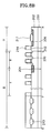
- FIG. 1 is a layout diagram illustrating a memory cell of a conventional flat cell type mask ROM.
- the flat cell type mask ROM has been widely used in a fabrication method using a logic process.
- the flat cell type mask ROM includes: a substrate 100 where a memory cell array region I and a segment select region II are defined; a trench (not shown) formed at the outer portion of the memory cell array region I of the substrate 100 ; an element isolating film (not shown) filling up the trench; a plurality of buried layers 110 aligned on the resultant structure in a first direction by a predetermined interval; and a plurality of gates 114 aligned in a second direction to cross the buried layers 110 in an orthogonal direction.
- an isolation process is performed at the outer portion of the memory cell array region I to surround the whole memory cell array region I, instead of performing a LOCOS or STI process for isolating memory cells.
- a source/drain junction of the memory cell is the buried layer 110 formed before the gate process. It is thus unnecessary to isolate the junctions.
- a contact 122 of the buried layer junction does not exist in the memory cell array region I but in the segment select region II.
- a width of the gate 114 is a channel width of the memory cell.
- a size of the memory cell is about 4F 2 (‘F’ implies a minimum line width of photolithography), thereby improving integration, simplifying the whole process and cutting down production costs.
- the isolation process is performed to surround the whole memory cell array region by a trench STI, 2) Ti-Salicide or Co-Salicide is used as the gate formation material, and 3) Ti-Salicide or Co-Salicide identical to the gate formation material is employed as the source/drain junction.
- FIG. 2 is a flowchart showing a conventional flat cell type mask ROM process.
- the conventional method for fabricating the mask ROM includes: an isolation process for forming an element isolating film at the outer portion of a memory cell array region; a well formation process; a buried layer formation process; a process for forming a gate insulating film and gates in the memory cell array region and its peripheral region; a cell isolation ion implant process for implanting ions to the memory cell array region; a process for forming a source/drain in the gates of the peripheral region; a coding process; a process for forming a contact in a buried layer of a segment select region; and a bit line formation process.
- FIGS. 3 a through 3 c are cross-sectional diagrams, taken along lines AB, BC and CD of FIG. 1 .
- ‘a’ denotes an active region of the memory cell array region
- ‘b’ denotes a peripheral region which is the outer portion of the active region.
- a substrate 100 where a memory cell array region I and a segment select region II are defined.
- a trench 103 is formed by etching the outer portion of the active region (a) of the memory cell array region I of the substrate 100 . Thereafter, an insulating film such as an oxide silicon film is deposited over the resultant structure, and etched according to an etch back process or a chemical mechanical polishing process, to form an element isolating film 104 filling up the trench 103 .
- an insulating film such as an oxide silicon film is deposited over the resultant structure, and etched according to an etch back process or a chemical mechanical polishing process, to form an element isolating film 104 filling up the trench 103 .
- a well 102 is formed on the substrate 100 having the element isolating film 104 according to an impurity implant process.
- the element isolating film formation process may be performed after the well formation process, as depicted in FIG. 3 B.
- a photolithography process and an impurity implant process are sequentially carried out in the memory cell array region I and the segment select region II of the substrate 100 having the well 102 , thereby forming buried layers 110 , 111 aligned in one direction.
- a gate insulating layer 112 is positioned on the substrate 100 , to form gates 114 aligned in an orthogonal direction to the buried layers 110 , 111 .
- a cell isolation ion implant process is performed in the active region (a) of the memory cell array region I, a source/drain 130 is formed in the peripheral region (b), and a coding process is performed thereon.
- a protective film 120 is deposited on the substrate 100 , and a contact 122 serving as a passage to a bit line (not shown) to be formed according to a succeeding process is formed on the buried layer 111 of the segment select region II.
- bit line electrically connected to the buried layer 111 of the segment select region II through the contact 122 is formed, and thus fabrication of the mask ROM is finished.
- the element isolating film is formed according to the shallow trench isolation and the chemical mechanical polishing process.
- one segment of the memory cell consists of 32 word lines and 1024 bit lines.
- a size of the segment is decreased, an area of the memory cell having the same integration is increased.
- a height of the 32 word lines is approximately 64F.
- a height of the segment select end is about 12F
- a height of the segment is 76F
- a length of the 1024 bit lines is about 2048F. That is, a size of the segment is represented by ‘2048F ⁇ 76F’.
- the size of the segment is represented by ‘512F ⁇ 19 ⁇ m’.
- the memory cell is an aggregate of the segments. For example, 128 segments are required to compose a 4M bit memory cell array. Therefore, a size of the 4M bit memory cell is approximately ‘512F ⁇ 2432 ⁇ m’, which is a size of the active region composing a memory cell block.
- the buried layer is patterned in a minimum size allowable in the photolithography. It is thus difficult to pattern the buried layer in the boundary portion between the segment select region and the memory cell array region.
- a mask ROM including: a substrate where a memory cell array region and a segment select region are defined; first and second trenches respectively formed at the outer portion of the memory cell array region and at the outer portion of a buried layer formation region of the segment select region; an element isolating film and an isolating pattern respectively filling up the first and second trenches; a plurality of buried layers aligned on the substrate in a first direction by a predetermined interval, and surrounded by the isolating pattern; and a plurality of gates aligned in a second direction to cross the buried layers in an orthogonal direction.
- a method for fabricating a mask ROM including the steps of: providing a substrate where a memory cell array region and a segment select region are defined; forming an element isolating film and an isolating pattern at the outer portion of the memory cell array region and at the outer portion of a buried layer formation region of the segment select region; forming a plurality of buried layers aligned over the resultant structure in a first direction by a predetermined interval, and surrounded by the isolating pattern; and forming a plurality of gates aligned in a second direction to cross the buried layers in an orthogonal direction.
- FIG. 1 is a layout diagram illustrating a memory cell of a conventional flat cell type mask ROM
- FIG. 2 is a flowchart showing a conventional flat cell type mask ROM process
- FIGS. 3 a through 3 c are cross-sectional diagrams, taken along lines AB, BC and CD of FIG. 1;
- FIG. 4 is a layout diagram illustrating a memory cell of a flat cell type mask ROM in accordance with the present invention
- FIG. 5 is a layout diagram illustrating a segment select region in accordance with the present invention.
- FIG. 6 is a plan diagram illustrating a mask pattern for forming buried layers in the segment select region in accordance with the present invention.
- FIG. 7 is a plan diagram illustrating the buried layers in the segment select region in accordance with the present invention.
- FIGS. 8 a through 8 c are cross-sectional diagrams, taken along lines EF, FG and GH of FIG. 4 .
- FIG. 4 is a layout diagram illustrating a memory cell of a flat cell type mask ROM in accordance with the present invention
- FIG. 5 is a layout diagram illustrating a segment select region in accordance with the present invention.
- the flat cell type mask ROM includes: a substrate 200 where a memory cell array region and a segment select region are defined; first and second trenches 203 , 205 , as depicted in FIG. 8A, respectively formed at the outer portion of the memory cell array region and at the outer portion of a buried layer formation region of the segment select region; an first isolation film 204 and an isolating pattern 206 respectively filling up the first and second trenches 203 , 205 ; a plurality of buried layers 210 aligned on the substrate 200 in a first direction by a predetermined interval, and surrounded by the second isolation film 206 ; and a plurality of gate insulating layers 212 and gates 214 aligned in a second direction to cross the buried layers 210 in an orthogonal direction.
- FIGS. 8 a through 8 c are cross-sectional diagrams, taken along lines EF, FG and GH of FIG. 4 .
- ‘c’ denotes an active region of the memory cell array region
- ‘d’ denotes a peripheral region which is an outer portion of the active region.
- the substrate 200 where the memory cell array region III and the segment select region IV are defined.
- the first and second trenches 203 , 205 are formed by etching the outer portion of the active region (c) of the memory cell array region III, and the outer portion of a buried layer formation region of the segment select region IV.
- the first and second trenches 203 , 205 are etched at a depth of 3000 to 4000 ⁇ from the surface of the substrate 200 .
- an insulating film such as an oxide silicon film is deposited over the resultant structure having the first and second trenches 203 , 205 , and etched according to an etch back process or a chemical mechanical polishing process, to form the first isolation film 204 and the isolating pattern filling up the first and second trenches 203 , 205 .
- the first isolation film 204 is formed at the outer portion of the active region (c) of the memory cell array region III, for isolating the active region (c) from the peripheral region (d).
- the second isolation film 206 is formed in the segment select region IV, for isolating the succeeding segment select region IV from the buried layer of the memory cell array region III.
- a well 202 is formed on the substrate 200 having the first isolation film 204 and the second isolation film 206 according to an impurity implant process.
- the element isolating film formation process and the well formation process may be performed in an inverse order.
- a photolithography process and an impurity implant process are sequentially carried out on the substrate 200 having the well 202 , thereby forming buried layers 210 , 211 aligned in one direction.
- a pad oxide film and a nitride film are sequentially deposited on the substrate 200 having the well 202 .
- a photoresist film covering the buried layer formation region is formed by coating a photoresist film on the nitride film, and exposing and developing the photoresist film.
- the substrate 200 is exposed by removing the nitride film and the pad oxide film by using the photoresist film pattern, and impurities are ion-implanted thereto, thereby forming the buried layers 210 , 211 .
- Reference numeral 210 denote the buried layer formed in the memory cell array region III, and 211 denotes the buried layer formed in the second isolation film 206 of the segment select region IV.
- FIG. 6 is a plan diagram illustrating a mask pattern for forming the buried layers in the segment select region in accordance with the present invention
- FIG. 7 is a plan diagram illustrating the buried layers in the segment select region in accordance with the present invention.
- the buried layers 210 , 211 are patterned by using the mask pattern of FIG. 6 . However, as depicted in FIG. 7, ions are implanted to the mask pattern region except the isolating pattern region.
- a gate insulating layer 212 is positioned on the substrate 200 , to form gates 214 aligned in an orthogonal direction to the buried layers 210 , 211 .
- a cell isolation ion implant process is performed in the active region (c) of the memory cell array region III, a source/drain 230 is formed in the peripheral region (d), and a coding process is performed thereon.
- a protective film 220 is deposited on the substrate 200 and etched to form a contact 111 for exposing the buried layer 211 of the segment select region IV.
- the contact 222 serves as a passage to a bit line to be formed according to a succeeding process.
- bit line (not shown) electrically connected to the buried layer 211 of the segment select region IV through the contact 211 is formed, and thus fabrication of the mask ROM is finished.
- the isolating pattern is added in every segment which is the minimum unit of the flat cell memory array, and thus a transistor of the segment select region and a memory cell transistor of the memory cell array region are not influenced by the buried layers, thereby maintaining a homogeneous device property.
- the flat cell process is performed under the logic process conditions of a design rule below 0.25 ⁇ m.
- a size of the active region is reduced to the memory cell array region of the segment, which results in improved polishing uniformity of the chemical mechanical polishing process.
Abstract
Description
Claims (3)
Priority Applications (1)
| Application Number | Priority Date | Filing Date | Title |
|---|---|---|---|
| US10/803,422 US6989307B2 (en) | 2001-08-27 | 2004-03-18 | Mask ROM, and fabrication method thereof |
Applications Claiming Priority (2)
| Application Number | Priority Date | Filing Date | Title |
|---|---|---|---|
| KR10-2001-0051826A KR100401004B1 (en) | 2001-08-27 | 2001-08-27 | mask ROM and fabricating method thereof |
| KR2001-51826 | 2001-08-27 |
Related Child Applications (1)
| Application Number | Title | Priority Date | Filing Date |
|---|---|---|---|
| US10/803,422 Division US6989307B2 (en) | 2001-08-27 | 2004-03-18 | Mask ROM, and fabrication method thereof |
Publications (2)
| Publication Number | Publication Date |
|---|---|
| US20030038310A1 US20030038310A1 (en) | 2003-02-27 |
| US6734508B2 true US6734508B2 (en) | 2004-05-11 |
Family
ID=19713592
Family Applications (2)
| Application Number | Title | Priority Date | Filing Date |
|---|---|---|---|
| US10/039,364 Expired - Lifetime US6734508B2 (en) | 2001-08-27 | 2001-11-07 | Mask ROM, and fabrication method thereof |
| US10/803,422 Expired - Lifetime US6989307B2 (en) | 2001-08-27 | 2004-03-18 | Mask ROM, and fabrication method thereof |
Family Applications After (1)
| Application Number | Title | Priority Date | Filing Date |
|---|---|---|---|
| US10/803,422 Expired - Lifetime US6989307B2 (en) | 2001-08-27 | 2004-03-18 | Mask ROM, and fabrication method thereof |
Country Status (4)
| Country | Link |
|---|---|
| US (2) | US6734508B2 (en) |
| JP (1) | JP2003078038A (en) |
| KR (1) | KR100401004B1 (en) |
| TW (1) | TW529133B (en) |
Families Citing this family (1)
| Publication number | Priority date | Publication date | Assignee | Title |
|---|---|---|---|---|
| KR100698065B1 (en) | 2004-12-30 | 2007-03-23 | 동부일렉트로닉스 주식회사 | MaskROM, Method for Fabricating the Same and Method for Coding |
Citations (3)
| Publication number | Priority date | Publication date | Assignee | Title |
|---|---|---|---|---|
| US6034403A (en) | 1998-06-25 | 2000-03-07 | Acer Semiconductor Manufacturing, Inc. | High density flat cell mask ROM |
| US6087699A (en) * | 1995-06-23 | 2000-07-11 | Taiwan Semiconductor Manufacturing Company | Laminated gate mask ROM device |
| US6414346B1 (en) * | 2000-01-24 | 2002-07-02 | Nec Corporation | Semiconductor memory and manufacturing method thereof |
Family Cites Families (10)
| Publication number | Priority date | Publication date | Assignee | Title |
|---|---|---|---|---|
| JPS5870567A (en) * | 1981-10-22 | 1983-04-27 | Nippon Denso Co Ltd | Manufacture of semiconductor device |
| JPS6292362A (en) * | 1985-10-17 | 1987-04-27 | Toshiba Corp | Manufacture of semiconductor device |
| US5480822A (en) * | 1994-11-28 | 1996-01-02 | United Microelectronics Corporation | Method of manufacture of semiconductor memory device with multiple, orthogonally disposed conductors |
| US5815433A (en) * | 1994-12-27 | 1998-09-29 | Nkk Corporation | Mask ROM device with gate insulation film based in pad oxide film and/or nitride film |
| JP3193845B2 (en) * | 1995-05-24 | 2001-07-30 | シャープ株式会社 | Semiconductor device and manufacturing method thereof |
| JP3355083B2 (en) * | 1996-03-13 | 2002-12-09 | シャープ株式会社 | Method for manufacturing semiconductor device |
| DE19640235C2 (en) * | 1996-09-30 | 2001-10-25 | Infineon Technologies Ag | Semiconductor read-only memory with transistors running vertically in trench side walls and method for its production |
| US6057195A (en) * | 1998-05-22 | 2000-05-02 | Texas Instruments - Acer Incorporated | Method of fabricating high density flat cell mask ROM |
| JP3166723B2 (en) * | 1998-09-02 | 2001-05-14 | 日本電気株式会社 | Semiconductor device and method of manufacturing semiconductor device |
| US6569735B2 (en) * | 2001-03-20 | 2003-05-27 | Macronix International Co., Ltd. | Manufacturing method for isolation on non-volatile memory |
-
2001
- 2001-08-27 KR KR10-2001-0051826A patent/KR100401004B1/en not_active IP Right Cessation
- 2001-11-02 TW TW090127364A patent/TW529133B/en not_active IP Right Cessation
- 2001-11-07 US US10/039,364 patent/US6734508B2/en not_active Expired - Lifetime
-
2002
- 2002-02-04 JP JP2002026221A patent/JP2003078038A/en active Pending
-
2004
- 2004-03-18 US US10/803,422 patent/US6989307B2/en not_active Expired - Lifetime
Patent Citations (3)
| Publication number | Priority date | Publication date | Assignee | Title |
|---|---|---|---|---|
| US6087699A (en) * | 1995-06-23 | 2000-07-11 | Taiwan Semiconductor Manufacturing Company | Laminated gate mask ROM device |
| US6034403A (en) | 1998-06-25 | 2000-03-07 | Acer Semiconductor Manufacturing, Inc. | High density flat cell mask ROM |
| US6414346B1 (en) * | 2000-01-24 | 2002-07-02 | Nec Corporation | Semiconductor memory and manufacturing method thereof |
Also Published As
| Publication number | Publication date |
|---|---|
| KR20030018222A (en) | 2003-03-06 |
| JP2003078038A (en) | 2003-03-14 |
| US20040173857A1 (en) | 2004-09-09 |
| US6989307B2 (en) | 2006-01-24 |
| KR100401004B1 (en) | 2003-10-10 |
| US20030038310A1 (en) | 2003-02-27 |
| TW529133B (en) | 2003-04-21 |
Similar Documents
| Publication | Publication Date | Title |
|---|---|---|
| US5696019A (en) | Self-aligned trench isolation for memory array using sidewall spacers | |
| US5763309A (en) | Self-aligned isolation and planarization process for memory array | |
| US6849518B2 (en) | Dual trench isolation using single critical lithographic patterning | |
| JP4086790B2 (en) | Nonvolatile memory and manufacturing method thereof | |
| US6596608B2 (en) | Method of manufacturing non-volatile semiconductor memory device | |
| US6700143B2 (en) | Dummy structures that protect circuit elements during polishing | |
| US8325516B2 (en) | Semiconductor device with split gate memory cell and fabrication method thereof | |
| KR100251229B1 (en) | Advanced nor type read only memory and fabricating method thereof | |
| JP4266089B2 (en) | Manufacturing method of semiconductor memory device | |
| US7094644B2 (en) | Method for manufacturing a semiconductor device | |
| KR100404682B1 (en) | Method for manufacturing a silicide layer of flat cell memory device | |
| US20050124118A1 (en) | Structure and method of fabricating a transistor having a trench gate | |
| US6734508B2 (en) | Mask ROM, and fabrication method thereof | |
| US6765257B1 (en) | Implanted vertical source-line under straight stack for flash eprom | |
| US6995060B2 (en) | Fabrication of integrated circuit elements in structures with protruding features | |
| US6518131B1 (en) | Method for fabricating mask ROM | |
| US7190019B2 (en) | Integrated circuits with openings that allow electrical contact to conductive features having self-aligned edges | |
| JPH03194967A (en) | Manufacture of semiconductor non-volatile memory | |
| JP3361973B2 (en) | Semiconductor device manufacturing method and semiconductor device | |
| KR100486120B1 (en) | Method for forming of mos transistor | |
| JPH08321593A (en) | Read only memory and fabrication thereof | |
| JPH0897275A (en) | Semiconductor device |
Legal Events
| Date | Code | Title | Description |
|---|---|---|---|
| AS | Assignment |
Owner name: DONGBU ELECTRONICS CO., LTD., KOREA, REPUBLIC OF Free format text: ASSIGNMENT OF ASSIGNORS INTEREST;ASSIGNOR:LIM, MIN GYU;REEL/FRAME:012462/0231 Effective date: 20011107 |
|
| FEPP | Fee payment procedure |
Free format text: PAYOR NUMBER ASSIGNED (ORIGINAL EVENT CODE: ASPN); ENTITY STATUS OF PATENT OWNER: LARGE ENTITY Free format text: PAYER NUMBER DE-ASSIGNED (ORIGINAL EVENT CODE: RMPN); ENTITY STATUS OF PATENT OWNER: LARGE ENTITY |
|
| STCF | Information on status: patent grant |
Free format text: PATENTED CASE |
|
| AS | Assignment |
Owner name: DONGBUANAM SEMICONDUCTOR INC., KOREA, REPUBLIC OF Free format text: CHANGE OF NAME;ASSIGNOR:DONGBU ELECTRONICS CO., LTD.;REEL/FRAME:016069/0777 Effective date: 20041221 |
|
| FPAY | Fee payment |
Year of fee payment: 4 |
|
| FEPP | Fee payment procedure |
Free format text: PAYOR NUMBER ASSIGNED (ORIGINAL EVENT CODE: ASPN); ENTITY STATUS OF PATENT OWNER: LARGE ENTITY Free format text: PAYER NUMBER DE-ASSIGNED (ORIGINAL EVENT CODE: RMPN); ENTITY STATUS OF PATENT OWNER: LARGE ENTITY |
|
| FPAY | Fee payment |
Year of fee payment: 8 |
|
| FPAY | Fee payment |
Year of fee payment: 12 |
|
| AS | Assignment |
Owner name: DONGBU ELECTRONICS CO., LTD., KOREA, REPUBLIC OF Free format text: CHANGE OF NAME;ASSIGNOR:DONGBUANAM SEMICONDUCTOR INC.;REEL/FRAME:044526/0571 Effective date: 20060324 |
|
| AS | Assignment |
Owner name: DONGBU HITEK CO., LTD., KOREA, REPUBLIC OF Free format text: MERGER AND CHANGE OF NAME;ASSIGNORS:DONGBU ELECTRONICS CO., LTD.;DONGBU HITEK CO., LTD.;REEL/FRAME:044533/0523 Effective date: 20070503 |
|
| AS | Assignment |
Owner name: DB HITEK CO., LTD, KOREA, REPUBLIC OF Free format text: CHANGE OF NAME;ASSIGNOR:DONGBU HITEK CO., LTD.;REEL/FRAME:044555/0913 Effective date: 20171101 |