US6759858B2 - Integrated circuit test probe having ridge contact - Google Patents
Integrated circuit test probe having ridge contact Download PDFInfo
- Publication number
- US6759858B2 US6759858B2 US09/421,210 US42121099A US6759858B2 US 6759858 B2 US6759858 B2 US 6759858B2 US 42121099 A US42121099 A US 42121099A US 6759858 B2 US6759858 B2 US 6759858B2
- Authority
- US
- United States
- Prior art keywords
- probe
- probe tip
- tip
- shaft
- integrated circuit
- Prior art date
- Legal status (The legal status is an assumption and is not a legal conclusion. Google has not performed a legal analysis and makes no representation as to the accuracy of the status listed.)
- Expired - Lifetime
Links
- 239000000523 sample Substances 0.000 title claims abstract description 150
- 238000012360 testing method Methods 0.000 title claims abstract description 48
- 229910000679 solder Inorganic materials 0.000 claims abstract description 43
- 230000000149 penetrating effect Effects 0.000 claims abstract description 4
- 238000000034 method Methods 0.000 claims description 15
- 238000004891 communication Methods 0.000 claims description 3
- 238000012545 processing Methods 0.000 claims description 3
- 238000010998 test method Methods 0.000 claims description 2
- 239000004020 conductor Substances 0.000 claims 1
- 238000006073 displacement reaction Methods 0.000 claims 1
- 230000013011 mating Effects 0.000 claims 1
- 238000004140 cleaning Methods 0.000 abstract description 3
- 238000004806 packaging method and process Methods 0.000 description 6
- 238000013459 approach Methods 0.000 description 4
- 230000002950 deficient Effects 0.000 description 3
- 239000002184 metal Substances 0.000 description 3
- 230000007547 defect Effects 0.000 description 2
- 230000035515 penetration Effects 0.000 description 2
- 230000002393 scratching effect Effects 0.000 description 2
- 235000001674 Agaricus brunnescens Nutrition 0.000 description 1
- 230000006978 adaptation Effects 0.000 description 1
- 239000000463 material Substances 0.000 description 1
- 238000006748 scratching Methods 0.000 description 1
- 229910052710 silicon Inorganic materials 0.000 description 1
- 239000010703 silicon Substances 0.000 description 1
Images


Classifications
-
- G—PHYSICS
- G01—MEASURING; TESTING
- G01R—MEASURING ELECTRIC VARIABLES; MEASURING MAGNETIC VARIABLES
- G01R1/00—Details of instruments or arrangements of the types included in groups G01R5/00 - G01R13/00 and G01R31/00
- G01R1/02—General constructional details
- G01R1/06—Measuring leads; Measuring probes
- G01R1/067—Measuring probes
- G01R1/06711—Probe needles; Cantilever beams; "Bump" contacts; Replaceable probe pins
- G01R1/06733—Geometry aspects
- G01R1/06738—Geometry aspects related to tip portion
-
- G—PHYSICS
- G01—MEASURING; TESTING
- G01R—MEASURING ELECTRIC VARIABLES; MEASURING MAGNETIC VARIABLES
- G01R31/00—Arrangements for testing electric properties; Arrangements for locating electric faults; Arrangements for electrical testing characterised by what is being tested not provided for elsewhere
- G01R31/28—Testing of electronic circuits, e.g. by signal tracer
- G01R31/2851—Testing of integrated circuits [IC]
- G01R31/2886—Features relating to contacting the IC under test, e.g. probe heads; chucks
Definitions
- the present invention relates generally to integrated circuits and in particular the present invention relates to electrical probes used to test integrated circuits.
- Integrated circuits are typically fabricated in a wafer of dies. Each die includes complex circuitry that will be separated from the die and further processed to allow for external electrical communication interconnects to the die. Because the die are complex, defects contained in the individual die can be severe and result in a die that is either scrap or requires some type of repair.
- a process of testing the integrated circuit die prior to packaging is typically performed to identify die that should not be further processed. This test is commonly referred to as wafer probe test, or die test. During a probe test a number of electrically conductive probes are placed in contact with conductive locations on the die. A relatively complete electrical testing can be conducted using the electrical probes.
- wire bond pads were located along a periphery of the circuit die and test probes could approach the die from an angled position.
- the angled approach assisted in “scratching” the test probe on the wire bond pads.
- the scratching action helped to break through any oxide layer which may have formed on the conductive layer. A lower resistance contact, therefore, could be provided between the probe and the conductive pad if the oxide layer were penetrated.
- an integrated circuit test probe comprises a probe shaft, and a downwardly extending probe tip attached to a bottom end of the probe shaft.
- the probe tip has an elongated pyramid shape.
- an integrated circuit test probe comprises a probe shaft, and a downwardly extending probe tip attached to a bottom end of the probe shaft.
- the probe tip has a blade-shape and comprises first, second, third and fourth downwardly extending sides, the first, second, third and fourth downwardly extending sides are connected on a downward edge to form a blade ridge.
- a method of testing an integrated circuit die comprises lowering a test probe onto a conductive pad located on the integrated circuit die, where a top surface of the conductive pad is covered with a layer of solder.
- the test probe comprises a probe shaft having an elbow, and a downwardly extending probe tip attached to a bottom end of the probe shaft, the probe tip has an elongated pyramid shape. A downward force is applied on the probe shaft, and the probe shaft is deflected such that a horizontal force is applied to the probe tip to create a cutting action between the probe tip and the layer of solder to penetrate the solder layer with the probe tip.
- FIG. 1 is a prior art flat tip test probe
- FIG. 2 is a side view of a test probe according to one embodiment of the present invention.
- FIG. 3 is a bottom perspective view of one embodiment of the present invention.
- FIG. 4A is a bottom view of one embodiment of the present invention.
- FIG. 4B is a bottom view of another embodiment of the present invention.
- FIG. 4C is a bottom view of another embodiment of the present invention.
- FIG. 5 is a side view of a test probe as applied to an integrated circuit conductive bump
- FIG. 6 is a more detailed illustration of a test probe as applied to an integrated circuit conductive bump.
- FIG. 7 provides a simplified illustration of a tester and probe card according to the present invention.
- integrated circuit die are tested prior to packaging to identify die which may be defective. If a defective die is detected, further processing expenses can be avoided.
- Integrated circuit die mounting techniques have evolved to allow for the distribution of mounting pads over the surface of the integrated circuit. These techniques often include the use of solder bumps formed on the conductive pads.
- the die can include solder located on the pads prior to performing a probe test. A layer of oxide on top of solder bumps can increase the resistance between the probe and the conductive bumps. The amount of resistance is typically influenced most by the surface of the solder. A probe that penetrates the solder surface, therefore, can have a lower resistance contact with the bumps.
- FIG. 1 illustrates an example prior art probe 100 used to test an integrated circuit die.
- the integrated circuit die includes a conductive bump 104 which has a generally mushroom top shape which is formed by a structure of solder plated on a metal layer 114 .
- the integrated circuit includes a base layer 100 , such as silicon, with multiple layers of material 108 and 110 which define specific structures and openings. A desired contact region 112 is exposed through the multiple layers such that a layer of metal 114 can be provided on top of the contact region. The solder is then provided in the opening of layer 110 and on top of the metal layer 114 .
- the specific method described to fabricate the solder bump is intended to be an example of one method of forming solder bumps, and other methods can be used without departing from the present invention.
- the probe includes a tip 102 which is used to make an electrical connection with the solder.
- the probe tip has a generally flat surface that is placed in contact with the solder. As explained, it is desired to penetrate the surface of the solder to form a reliable connection for testing. Variations in the probe to pad resistance can create erroneous data during testing. By adding a slight horizontal movement to the probe while making contact with the pad, the surface of the solder can be broken by the probe tip. The probe tip, however, accumulates solder oxidized residue over time. This oxidized solder residue can increase the probe tip resistance and create erroneous test data. As a result, the test probes must be periodically cleaned to remove any solder residue.
- the probe 120 includes a probe shaft 122 and a tip 124 which is attached to a bottom end of the shaft.
- the probe tip is shaped with a pointed surface.
- the tip is illustrated in FIG. 3 to show the tip as an elongated pyramid.
- the pyramid shape illustrated has four defined sides, however, the shape can be modified to have three or two sides and still maintain a shape having a ridge. These tips can also be called “blade” tips.
- the tip downwardly extends from the shaft.
- the tip can include a circular plate, or base, 123 which provides a secure connection to the shaft.
- FIG. 4A illustrates a bottom view of the blade tip having four sides.
- the tip illustrated is one embodiment of a tip according to the present invention.
- the tip includes four sides, 130 , 131 , 132 and 134 .
- the four sides form a center ridge, or blade, 136 .
- the height of the tip from plate 123 to the ridge can be selected for the type of pad/solder being tested. In one embodiment, the tip height is about 1.5 mil.
- FIG. 4B illustrates a bottom view of a blade tip having three sides 140 , 141 and 142 . The three sides form a ridge 143 .
- FIG. 4C illustrates a bottom view of a blade tip having two sides 145 and 146 which form a ridge 147 .
- probe 120 is lowered in a vertical direction 150 onto a solder bump 202 .
- the probe tip is then moved in a horizontal direction 160 to assist in penetrating the solder.
- the shaft includes at least one slight elbow 155 . This bend provides the horizontal movement to the blade tip as the probe is forced in the vertical direction. That is, the shaft will deflect slightly at the elbow to move the tip in direction 160 .
- the horizontal movement is directed along the central line of the probe tip as defined by ridge 136 and the movement is about 0.5-1.5 mil in length. This movement “cuts” into the solder to provide a reduced resistance contact between the probe and the solder/conductive bump.
- the tip creates a small groove in the solder layer.
- the leading edge 132 of the probe tip can be either rounded or formed with a point.
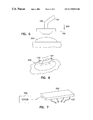
- FIG. 7 illustrates a simplified probe card 250 coupled to a tester 252 .
- the probe card includes numerous probes 122 which are custom designed for the layout and specifications of the integrated circuit die that is to be tested with the probe card. About 1500 probes are included in a probe card for a “typical” microprocessor die. The next generation of high speed processors may push the envelope to 2000 and 3000 probes per card.
- the ‘blade’ tip shape provides several benefits over the traditional “flat” tip.
- the term flat is used herein to refer to tips with a flat or slightly convex surface.
- the shape of the probe tip reduces solder residue buildup on the probe tip. That is, the blade shape cuts into the solder and allows the solder to effectively slide along sides 131 and 133 of the tip without creating a residue buildup. As such, expensive and time consuming tip cleaning is reduced, if not eliminated.
- the tip increases solder penetration to provide a more consistent contact resistance while testing numerous integrated circuit die.
- An integrated circuit die test probe has been described which has a non-flat tip.
- the tip has an elongated pyramid shape that provides a cutting action while probing solder covered conductive pads.
- the tip shape helps maintain a uniform tip to bump resistance during testing by penetrating the solder layer and avoiding solder residue build up.
- the test probes significantly reduce the need for cleaning the probe tips to remove residue.
Abstract
Description
Claims (20)
Priority Applications (1)
| Application Number | Priority Date | Filing Date | Title |
|---|---|---|---|
| US09/421,210 US6759858B2 (en) | 1999-10-20 | 1999-10-20 | Integrated circuit test probe having ridge contact |
Applications Claiming Priority (1)
| Application Number | Priority Date | Filing Date | Title |
|---|---|---|---|
| US09/421,210 US6759858B2 (en) | 1999-10-20 | 1999-10-20 | Integrated circuit test probe having ridge contact |
Publications (2)
| Publication Number | Publication Date |
|---|---|
| US20020017914A1 US20020017914A1 (en) | 2002-02-14 |
| US6759858B2 true US6759858B2 (en) | 2004-07-06 |
Family
ID=23669614
Family Applications (1)
| Application Number | Title | Priority Date | Filing Date |
|---|---|---|---|
| US09/421,210 Expired - Lifetime US6759858B2 (en) | 1999-10-20 | 1999-10-20 | Integrated circuit test probe having ridge contact |
Country Status (1)
| Country | Link |
|---|---|
| US (1) | US6759858B2 (en) |
Cited By (12)
| Publication number | Priority date | Publication date | Assignee | Title |
|---|---|---|---|---|
| US20040177499A1 (en) * | 1998-11-10 | 2004-09-16 | Eldridge Benjamin N. | Tested semiconductor device produced by an interconnection element with contact blade |
| US20040239348A1 (en) * | 2003-05-28 | 2004-12-02 | Barr Andrew Harvey | Tip and tip assembly for a signal probe |
| US20060081785A1 (en) * | 2003-02-14 | 2006-04-20 | Bjorn Heismann | X-ray detector |
| US7112974B1 (en) * | 2002-05-23 | 2006-09-26 | Cypress Semiconductor Corporation | Proble for testing integrated circuits |
| US20070257687A1 (en) * | 2005-04-22 | 2007-11-08 | Alexander Leon | Methods Of Using A Blade Probe For Probing A Node Of A Circuit |
| US20070262784A1 (en) * | 2005-04-22 | 2007-11-15 | Alexander Leon | Arcuate blade probe |
| US7319341B1 (en) * | 2003-08-28 | 2008-01-15 | Altera Corporation | Method of maintaining signal integrity across a capacitive coupled solder bump |
| US20080094084A1 (en) * | 2006-10-24 | 2008-04-24 | Industrial Technology Research Institute | Multi-layer electric probe and fabricating method thereof |
| US20080110019A1 (en) * | 2004-03-26 | 2008-05-15 | Nulty James E | Probe card and method for constructing same |
| US20090058445A1 (en) * | 2005-04-22 | 2009-03-05 | Alexander Leon | Circuit board testing using a probe |
| US20090096473A1 (en) * | 2007-10-16 | 2009-04-16 | Compal Electronics, Inc. | Testing probe and electrical connection method using the same |
| US20180238932A1 (en) * | 2016-02-15 | 2018-08-23 | Nhk Spring Co., Ltd. | Conductive probe for inspection and semiconductor inspection device |
Families Citing this family (8)
| Publication number | Priority date | Publication date | Assignee | Title |
|---|---|---|---|---|
| US7266151B2 (en) * | 2002-09-04 | 2007-09-04 | Intel Corporation | Method and system for performing motion estimation using logarithmic search |
| US20040042551A1 (en) * | 2002-09-04 | 2004-03-04 | Tinku Acharya | Motion estimation |
| US20040057626A1 (en) * | 2002-09-23 | 2004-03-25 | Tinku Acharya | Motion estimation using a context adaptive search |
| US9716031B2 (en) * | 2014-04-08 | 2017-07-25 | Nxp Usa, Inc. | Semiconductor wafer and method of concurrently testing circuits formed thereon |
| KR20180044725A (en) * | 2016-10-24 | 2018-05-03 | 주식회사 엘지화학 | The shunt resistor for measuring current |
| JP7000966B2 (en) * | 2018-04-04 | 2022-01-19 | 株式会社デンソー | Switch overcurrent detection circuit |
| JP7056449B2 (en) * | 2018-08-01 | 2022-04-19 | トヨタ自動車株式会社 | Inspection device for power storage device |
| US10725192B2 (en) * | 2018-10-10 | 2020-07-28 | United States Of America, As Represented By The Secretary Of The Navy | Passive magnetic field detector |
Citations (25)
| Publication number | Priority date | Publication date | Assignee | Title |
|---|---|---|---|---|
| US3611128A (en) * | 1968-07-26 | 1971-10-05 | Hitachi Ltd | Probe header for testing integrated circuits |
| US3996516A (en) * | 1973-08-23 | 1976-12-07 | Lm-Electronic Luther & Maelzer | Apparatus and process for testing printed circuits |
| US4001685A (en) * | 1974-03-04 | 1977-01-04 | Electroglas, Inc. | Micro-circuit test probe |
| US4034293A (en) * | 1974-03-04 | 1977-07-05 | Electroglas, Inc. | Micro-circuit test probe |
| US4161692A (en) * | 1977-07-18 | 1979-07-17 | Cerprobe Corporation | Probe device for integrated circuit wafers |
| US4195259A (en) * | 1978-04-04 | 1980-03-25 | Texas Instruments Incorporated | Multiprobe test system and method of using same |
| US4468615A (en) * | 1980-03-26 | 1984-08-28 | Societe d'Etudes Techniques et d'Enterprises Generales Transmission Automatique & Informatique - Sodeteg Tai | Probe for a printed-circuit testing device, and a testing device incorporating said probe |
| US4937653A (en) * | 1988-07-21 | 1990-06-26 | American Telephone And Telegraph Company | Semiconductor integrated circuit chip-to-chip interconnection scheme |
| US4954458A (en) * | 1982-06-03 | 1990-09-04 | Texas Instruments Incorporated | Method of forming a three dimensional integrated circuit structure |
| US4965865A (en) * | 1989-10-11 | 1990-10-23 | General Signal Corporation | Probe card for integrated circuit chip |
| US5113133A (en) * | 1990-12-20 | 1992-05-12 | Integri-Test Corporation | Circuit board test probe |
| US5323035A (en) * | 1992-10-13 | 1994-06-21 | Glenn Leedy | Interconnection structure for integrated circuits and method for making same |
| US5326428A (en) * | 1993-09-03 | 1994-07-05 | Micron Semiconductor, Inc. | Method for testing semiconductor circuitry for operability and method of forming apparatus for testing semiconductor circuitry for operability |
| US5367165A (en) * | 1992-01-17 | 1994-11-22 | Olympus Optical Co., Ltd. | Cantilever chip for scanning probe microscope |
| US5546405A (en) * | 1995-07-17 | 1996-08-13 | Advanced Micro Devices, Inc. | Debug apparatus for an automated semiconductor testing system |
| US5559444A (en) * | 1991-06-04 | 1996-09-24 | Micron Technology, Inc. | Method and apparatus for testing unpackaged semiconductor dice |
| US5731710A (en) * | 1993-12-24 | 1998-03-24 | Nippondenso Co., Ltd. | Contact probe apparatus used in electric tests for a circuit board |
| US5763879A (en) * | 1996-09-16 | 1998-06-09 | Pacific Western Systems | Diamond probe tip |
| US5821763A (en) * | 1992-10-19 | 1998-10-13 | International Business Machines Corporation | Test probe for high density integrated circuits, methods of fabrication thereof and methods of use thereof |
| US6016060A (en) * | 1997-03-25 | 2000-01-18 | Micron Technology, Inc. | Method, apparatus and system for testing bumped semiconductor components |
| US6037786A (en) * | 1996-12-13 | 2000-03-14 | International Business Machines Corporation | Testing integrated circuit chips |
| US6206273B1 (en) * | 1999-02-17 | 2001-03-27 | International Business Machines Corporation | Structures and processes to create a desired probetip contact geometry on a wafer test probe |
| US6256882B1 (en) * | 1998-07-14 | 2001-07-10 | Cascade Microtech, Inc. | Membrane probing system |
| US6362637B2 (en) * | 1996-12-31 | 2002-03-26 | Micron Technology, Inc. | Apparatus for testing semiconductor wafers including base with contact members and terminal contacts |
| US6414506B2 (en) * | 1993-09-03 | 2002-07-02 | Micron Technology, Inc. | Interconnect for testing semiconductor dice having raised bond pads |
-
1999
- 1999-10-20 US US09/421,210 patent/US6759858B2/en not_active Expired - Lifetime
Patent Citations (25)
| Publication number | Priority date | Publication date | Assignee | Title |
|---|---|---|---|---|
| US3611128A (en) * | 1968-07-26 | 1971-10-05 | Hitachi Ltd | Probe header for testing integrated circuits |
| US3996516A (en) * | 1973-08-23 | 1976-12-07 | Lm-Electronic Luther & Maelzer | Apparatus and process for testing printed circuits |
| US4001685A (en) * | 1974-03-04 | 1977-01-04 | Electroglas, Inc. | Micro-circuit test probe |
| US4034293A (en) * | 1974-03-04 | 1977-07-05 | Electroglas, Inc. | Micro-circuit test probe |
| US4161692A (en) * | 1977-07-18 | 1979-07-17 | Cerprobe Corporation | Probe device for integrated circuit wafers |
| US4195259A (en) * | 1978-04-04 | 1980-03-25 | Texas Instruments Incorporated | Multiprobe test system and method of using same |
| US4468615A (en) * | 1980-03-26 | 1984-08-28 | Societe d'Etudes Techniques et d'Enterprises Generales Transmission Automatique & Informatique - Sodeteg Tai | Probe for a printed-circuit testing device, and a testing device incorporating said probe |
| US4954458A (en) * | 1982-06-03 | 1990-09-04 | Texas Instruments Incorporated | Method of forming a three dimensional integrated circuit structure |
| US4937653A (en) * | 1988-07-21 | 1990-06-26 | American Telephone And Telegraph Company | Semiconductor integrated circuit chip-to-chip interconnection scheme |
| US4965865A (en) * | 1989-10-11 | 1990-10-23 | General Signal Corporation | Probe card for integrated circuit chip |
| US5113133A (en) * | 1990-12-20 | 1992-05-12 | Integri-Test Corporation | Circuit board test probe |
| US5559444A (en) * | 1991-06-04 | 1996-09-24 | Micron Technology, Inc. | Method and apparatus for testing unpackaged semiconductor dice |
| US5367165A (en) * | 1992-01-17 | 1994-11-22 | Olympus Optical Co., Ltd. | Cantilever chip for scanning probe microscope |
| US5323035A (en) * | 1992-10-13 | 1994-06-21 | Glenn Leedy | Interconnection structure for integrated circuits and method for making same |
| US5821763A (en) * | 1992-10-19 | 1998-10-13 | International Business Machines Corporation | Test probe for high density integrated circuits, methods of fabrication thereof and methods of use thereof |
| US5326428A (en) * | 1993-09-03 | 1994-07-05 | Micron Semiconductor, Inc. | Method for testing semiconductor circuitry for operability and method of forming apparatus for testing semiconductor circuitry for operability |
| US6414506B2 (en) * | 1993-09-03 | 2002-07-02 | Micron Technology, Inc. | Interconnect for testing semiconductor dice having raised bond pads |
| US5731710A (en) * | 1993-12-24 | 1998-03-24 | Nippondenso Co., Ltd. | Contact probe apparatus used in electric tests for a circuit board |
| US5546405A (en) * | 1995-07-17 | 1996-08-13 | Advanced Micro Devices, Inc. | Debug apparatus for an automated semiconductor testing system |
| US5763879A (en) * | 1996-09-16 | 1998-06-09 | Pacific Western Systems | Diamond probe tip |
| US6037786A (en) * | 1996-12-13 | 2000-03-14 | International Business Machines Corporation | Testing integrated circuit chips |
| US6362637B2 (en) * | 1996-12-31 | 2002-03-26 | Micron Technology, Inc. | Apparatus for testing semiconductor wafers including base with contact members and terminal contacts |
| US6016060A (en) * | 1997-03-25 | 2000-01-18 | Micron Technology, Inc. | Method, apparatus and system for testing bumped semiconductor components |
| US6256882B1 (en) * | 1998-07-14 | 2001-07-10 | Cascade Microtech, Inc. | Membrane probing system |
| US6206273B1 (en) * | 1999-02-17 | 2001-03-27 | International Business Machines Corporation | Structures and processes to create a desired probetip contact geometry on a wafer test probe |
Non-Patent Citations (2)
| Title |
|---|
| Merriam-Wesster's College Dictionary, Tenth Edition., 1998.* * |
| Walker, Chambers Dictionary of Science and Technology, general edition, 1999. * |
Cited By (19)
| Publication number | Priority date | Publication date | Assignee | Title |
|---|---|---|---|---|
| US9030222B2 (en) | 1998-11-10 | 2015-05-12 | Formfactor, Inc. | Sharpened, oriented contact tip structures |
| US20040177499A1 (en) * | 1998-11-10 | 2004-09-16 | Eldridge Benjamin N. | Tested semiconductor device produced by an interconnection element with contact blade |
| US7112974B1 (en) * | 2002-05-23 | 2006-09-26 | Cypress Semiconductor Corporation | Proble for testing integrated circuits |
| US20060081785A1 (en) * | 2003-02-14 | 2006-04-20 | Bjorn Heismann | X-ray detector |
| US20040239348A1 (en) * | 2003-05-28 | 2004-12-02 | Barr Andrew Harvey | Tip and tip assembly for a signal probe |
| US6937039B2 (en) * | 2003-05-28 | 2005-08-30 | Hewlett-Packard Development Company, L.P. | Tip and tip assembly for a signal probe |
| US7319341B1 (en) * | 2003-08-28 | 2008-01-15 | Altera Corporation | Method of maintaining signal integrity across a capacitive coupled solder bump |
| US20080110019A1 (en) * | 2004-03-26 | 2008-05-15 | Nulty James E | Probe card and method for constructing same |
| US7685705B2 (en) | 2004-03-26 | 2010-03-30 | Cypress Semiconductor Corporation | Method of fabricating a probe card |
| US20090058445A1 (en) * | 2005-04-22 | 2009-03-05 | Alexander Leon | Circuit board testing using a probe |
| US7453278B2 (en) * | 2005-04-22 | 2008-11-18 | Hewlett-Packard Development Company, L.P. | Methods of using a blade probe for probing a node of a circuit |
| US7463046B2 (en) * | 2005-04-22 | 2008-12-09 | Hewlett-Packard Development Company, L.P. | Arcuate blade probe with means for aligning the barrel and the shaft |
| US20070262784A1 (en) * | 2005-04-22 | 2007-11-15 | Alexander Leon | Arcuate blade probe |
| US8253430B2 (en) | 2005-04-22 | 2012-08-28 | Hewlett-Packard Development Company | Circuit board testing using a probe |
| US20070257687A1 (en) * | 2005-04-22 | 2007-11-08 | Alexander Leon | Methods Of Using A Blade Probe For Probing A Node Of A Circuit |
| US20080094084A1 (en) * | 2006-10-24 | 2008-04-24 | Industrial Technology Research Institute | Multi-layer electric probe and fabricating method thereof |
| US20090096473A1 (en) * | 2007-10-16 | 2009-04-16 | Compal Electronics, Inc. | Testing probe and electrical connection method using the same |
| US20180238932A1 (en) * | 2016-02-15 | 2018-08-23 | Nhk Spring Co., Ltd. | Conductive probe for inspection and semiconductor inspection device |
| US10274517B2 (en) * | 2016-02-15 | 2019-04-30 | Nhk Spring Co., Ltd. | Conductive probe for inspection and semiconductor inspection device |
Also Published As
| Publication number | Publication date |
|---|---|
| US20020017914A1 (en) | 2002-02-14 |
Similar Documents
| Publication | Publication Date | Title |
|---|---|---|
| US6759858B2 (en) | Integrated circuit test probe having ridge contact | |
| US7005870B2 (en) | Interconnect bump plate | |
| EP0545070A1 (en) | Membrane probe contact bump compliancy system | |
| US6100708A (en) | Probe card and wafer testing method using the same | |
| JPH04233480A (en) | Flexible-tape type probe | |
| US6433571B1 (en) | Process for testing a semiconductor device | |
| KR101019554B1 (en) | Probe and menufacturing method of the same | |
| US5338223A (en) | Hybrid wafer probe | |
| US6784556B2 (en) | Design of interconnection pads with separated probing and wire bonding regions | |
| US20070035318A1 (en) | Donut-type parallel probe card and method of testing semiconductor wafer using same | |
| US6121784A (en) | Probe tip and a process for testing a semiconductor device | |
| US7474113B2 (en) | Flexible head probe for sort interface units | |
| JPH08285890A (en) | Probe card | |
| KR100621760B1 (en) | probe card for testing semiconductor chip | |
| US6650133B1 (en) | Method and apparatus for buckling beam testing | |
| JP3138366B2 (en) | Probe device | |
| JPS63128264A (en) | Probe card | |
| JPH0822875A (en) | Ic socket | |
| JP3261723B2 (en) | Semiconductor wafer pellet inspection method | |
| JPH0980116A (en) | Socket for semiconductor chip | |
| JPH0637137A (en) | Electrode structure of semiconductor wafer | |
| KR20010051757A (en) | Ultrasonic assist of semiconductor device multi-probe testing | |
| KR19980020299A (en) | Probe tip on wafer test device for reduced contact resistance | |
| JPS61226938A (en) | Testing device for semiconductor device | |
| JPH10253662A (en) | Probe card |
Legal Events
| Date | Code | Title | Description |
|---|---|---|---|
| AS | Assignment |
Owner name: INTEL CORPORATION, CALIFORNIA Free format text: ASSIGNMENT OF ASSIGNORS INTEREST;ASSIGNOR:ROGGEL, AMIR;REEL/FRAME:010331/0023 Effective date: 19991008 |
|
| STCF | Information on status: patent grant |
Free format text: PATENTED CASE |
|
| FEPP | Fee payment procedure |
Free format text: PAYOR NUMBER ASSIGNED (ORIGINAL EVENT CODE: ASPN); ENTITY STATUS OF PATENT OWNER: LARGE ENTITY |
|
| FPAY | Fee payment |
Year of fee payment: 4 |
|
| REMI | Maintenance fee reminder mailed | ||
| FPAY | Fee payment |
Year of fee payment: 8 |
|
| AS | Assignment |
Owner name: BEIJING XIAOMI MOBILE SOFTWARE CO., LTD., CHINA Free format text: ASSIGNMENT OF ASSIGNORS INTEREST;ASSIGNOR:INTEL CORPORATION;REEL/FRAME:037733/0440 Effective date: 20160204 |
|
| REMI | Maintenance fee reminder mailed | ||
| FPAY | Fee payment |
Year of fee payment: 12 |
|
| SULP | Surcharge for late payment |
Year of fee payment: 11 |