US6759859B2 - Resilient and rugged multi-layered probe - Google Patents

Resilient and rugged multi-layered probe Download PDF

Info

Publication number
US6759859B2
US6759859B2 US10/033,749 US3374901A US6759859B2 US 6759859 B2 US6759859 B2 US 6759859B2 US 3374901 A US3374901 A US 3374901A US 6759859 B2 US6759859 B2 US 6759859B2
Authority
US
United States
Prior art keywords
probe
resilient
transmission structure
rugged
probe tip
Prior art date
Legal status (The legal status is an assumption and is not a legal conclusion. Google has not performed a legal analysis and makes no representation as to the accuracy of the status listed.)
Expired - Lifetime
Application number
US10/033,749
Other versions
US20030112024A1 (en
Inventor
Joseph D. S. Deng
Hong-Chyi Lee
Current Assignee (The listed assignees may be inaccurate. Google has not performed a legal analysis and makes no representation or warranty as to the accuracy of the list.)
National Chung Shan Institute of Science and Technology NCSIST
Original Assignee
National Chung Shan Institute of Science and Technology NCSIST
Priority date (The priority date is an assumption and is not a legal conclusion. Google has not performed a legal analysis and makes no representation as to the accuracy of the date listed.)
Filing date
Publication date
Application filed by National Chung Shan Institute of Science and Technology NCSIST filed Critical National Chung Shan Institute of Science and Technology NCSIST
Priority to US10/033,749 priority Critical patent/US6759859B2/en
Assigned to CHUNG-SHAN INSTITUTE OF SCIENCE AND TECHNOLOGY reassignment CHUNG-SHAN INSTITUTE OF SCIENCE AND TECHNOLOGY ASSIGNMENT OF ASSIGNORS INTEREST (SEE DOCUMENT FOR DETAILS). Assignors: DENG, JOSEPH D.S., LEE, HONG-CHYI
Publication of US20030112024A1 publication Critical patent/US20030112024A1/en
Priority to US10/818,958 priority patent/US6930497B2/en
Application granted granted Critical
Publication of US6759859B2 publication Critical patent/US6759859B2/en
Assigned to NATIONAL CHUNG SHAN INSTITUTE OF SCIENCE AND TECHNOLOGY reassignment NATIONAL CHUNG SHAN INSTITUTE OF SCIENCE AND TECHNOLOGY CHANGE OF NAME (SEE DOCUMENT FOR DETAILS). Assignors: CHUNG-SHAN INSTITUTE OF SCIENCE AND TECHNOLOGY
Anticipated expiration legal-status Critical
Expired - Lifetime legal-status Critical Current

Links

Images

Classifications

    • GPHYSICS
    • G01MEASURING; TESTING
    • G01RMEASURING ELECTRIC VARIABLES; MEASURING MAGNETIC VARIABLES
    • G01R1/00Details of instruments or arrangements of the types included in groups G01R5/00 - G01R13/00 and G01R31/00
    • G01R1/02General constructional details
    • G01R1/06Measuring leads; Measuring probes
    • G01R1/067Measuring probes
    • G01R1/06772High frequency probes
    • GPHYSICS
    • G01MEASURING; TESTING
    • G01RMEASURING ELECTRIC VARIABLES; MEASURING MAGNETIC VARIABLES
    • G01R1/00Details of instruments or arrangements of the types included in groups G01R5/00 - G01R13/00 and G01R31/00
    • G01R1/02General constructional details
    • G01R1/06Measuring leads; Measuring probes
    • G01R1/067Measuring probes
    • G01R1/073Multiple probes
    • G01R1/07307Multiple probes with individual probe elements, e.g. needles, cantilever beams or bump contacts, fixed in relation to each other, e.g. bed of nails fixture or probe card
    • G01R1/07357Multiple probes with individual probe elements, e.g. needles, cantilever beams or bump contacts, fixed in relation to each other, e.g. bed of nails fixture or probe card with flexible bodies, e.g. buckling beams

Definitions

  • the invention relates in general to a probe, and more particularly, to a resilient and rugged probe used to measure microwave and high-speed signals on a wafer.
  • the versatile applications of microwave and high-speed signal circuit further include the hybrid circuit, the multi-chip module (MCM), and the integrated circuit (IC).
  • MCM multi-chip module
  • IC integrated circuit
  • the most accurate and convenient measurement methods include on-wafer measurement. To obtain an accurate measurement result, a good probe is required.
  • the signal transmission medium made of Al 2 O 3 has the characteristics of high microwave transmission quality and low transmission loss.
  • the supporting substrate is made of a hard material, the angle of depression between the probe and the object to be measured and the downward pressure applied to the probe is strictly specified during measurement. Therefore, the probe tip has to be held parallel to the object to be measured. Further, a limited range of pressure is applied to the probe while touching the object to avoid damaging the probe.
  • the probe tip has a claw shape to probe a planar transmission structure, so as to allow measuring a non-planar object.
  • a planar-coaxial converter is adjacent right behind the probe to output the signal to the measurement instrument thereby.
  • the microwave probe tip has one end made of metal in a claw shape and the other end in the form of a coaxial signal cable. Without a supporting medium and the resilience thereof, the claw-shape tip of the microwave probe can be shifted up and down within a limited range for measuring an object with an uneven or non-planar surface.
  • the angle of suppression for probing the object is still limited by the parameters of length and pitch of the probe tip. That is, the longer is the tip, the bigger is the angle tolerance and the larger is the pitch and the smaller is the angle tolerance.
  • a soft substrate is incorporated as the supporting material for the probe tip and the signal transmission planar structure. Such substrate allows the probe tip having angle difference (angle of suppression, angle of elevation) with the object to be measured.
  • substrates made of different materials are laminated into a composite substrate, of which a layer with a higher dielectric constant is harder and used as the dielectric for signal transmission planar structure, and another layer with a lower dielectric constant is softer and used for supporting and providing resilience.
  • the probe tip and the signal transmission planar structure are all on the composite substrate.
  • the probe is resilient and twistable during measurement.
  • the tolerance of the angles of suppression and elevation of the probe tip for measuring the object is increased.
  • the probe tip cannot be moved up and down separately. It is thus not applicable for object with an uneven surface.
  • the invention provides a resilient and rugged probe.
  • a soft and resilient high-frequency substrate and a suspended claw-shape probe tip are incorporated to resolve the unevenness problems of the circuit substrate and the poor surrounding planarity. The accuracy and reproducibility for measurement can thus be ensured.
  • the invention provides a resilient and rugged probe to measure the on-wafer signal.
  • the probe has a metal probe tip, a resilient soft multi-layered dielectric substrate, a planar transmission structure and a fixed end.
  • the probe tip is connected to the planar transmission structure.
  • the planar transmission structure is attached to and supported by the resilient soft multi-layered dielectric substrate, and then is connected to the fixed end.
  • the metal probe tip is used to probe the signal of the wafer. Further, the metal tip is able to rotate about an axis with a specific angle and to lift or dive as required.
  • the fixed end supports and holds the probe, and is used as a transmission structure converter of the probe to connect the planar transmission structure to the coaxial transmission structure.
  • the invention further provides a resilient and rugged probe to measure signals on wafer.
  • the probe has a probe tip, a planar transmission structure and a multi-layered dielectric material.
  • the probe tip is connected to the planar transmission structure.
  • the multi-layered dielectric substrate supports the planar transmission structure.
  • Devices can be embedded into the multi-layered dielectric material.
  • the devices include multi-layered microwave circuits, vertical connectors, bias circuits, or matching circuit devices.
  • the probe tip is protrusive to probe the signal of the substrate.
  • the metal probe tip can rotate around an axis with a specific angle and can dive and lift.
  • the invention further provides a resilient and rugged probe to measure signals on wafer.
  • the probe has a probe tip, a connector and a multi-layered dielectric material.
  • the connector is attached to the fixed end to couple the signals from the probe to measurement instruments.
  • the multi-layered dielectric substrate supports the planar transmission structure.
  • Devices can be embedded into the multi-layered dielectric material.
  • the devices include multi-layered microwave circuit, vertical connector or matching circuit device.
  • the probe provided by the invention can be bent to a configuration conformal to the measuring object, and the probe can apply pressure to the probe tip to provide the advantages of high measurement repeatability, operation convenience and ruggedness.
  • FIG. 1A shows a side view of an embodiment of a resilient and rugged probe provided by the present invention
  • FIG. 1B shows movements of the resilient and rugged probe
  • FIG. 1C is a bottom view of the resilient and rugged probe
  • FIG. 3 shows the contact repeatability vs. frequency graph of measurement result using the resilient and rugged probe provided by the invention
  • FIG. 5A is a cross sectional view showing a resilient and rugged probe in another embodiment.
  • FIG. 5B is a bottom view of the resilient and rugged probe.
  • the structure of a resilient and rugged probe in one embodiment is shown.
  • the probe 10 is used to measure the on-wafer signal.
  • the probe 10 includes a metal probe tip 102 , a resilient soft multi-layered dielectric substrate 104 , a planar transmission structure 106 , and a fixed end 108 for supporting the probe 10 .
  • the metal probe tip 102 extends outward and suspends from the planar transmission structure into the surrounding air and has a claw shape.
  • the probe tip 102 can move up and down and rotate within a limited range while measuring an uneven or non-planar object. The object can then be probed and measured.
  • the planar transmission structure 106 is coupled to the metal probe tip 102 and attached to the resilient soft multi-layered dielectric substrate 104 .
  • the fixed end 108 is coupled to the resilient soft multi-layered dielectric substrate 104 and the planar transmission structure 106 to support and hold the probe 10 , and functions as a transmission structure converter of the probe to collect the planar transmission structure 106 and the coaxial transmission structure 120 .
  • the coaxial transmission structure 120 is clearly illustrated from the bottom view of the probe 10 and an expanded view of the coaxial transmission structure 120 is shown on the right side.
  • the far end of the fixed end 108 that is, the metal probe tip 102 , allows movement of rotating 110 with an angle ⁇ and diving and lifting 112 with an anile ⁇ , as shown in FIGS. 2 and 4 respectively.
  • the multi-layered dielectric material 506 is coupled to the planar transmission structure 504 and the probe tip 502 .
  • Devices 508 could be embedded into the multi-layered dielectric material 506 .
  • the device 508 includes a multi-layered microwave circuit 520 , a vertical connector 522 or a matching circuit device 524 .
  • the probe 50 can designed as an impedance pre-matching type of probe attached with a bias network to measure the non-system impedance matching device or module.
  • the probe 50 can be assembled into a mixer type probe to analyze and measure the hybrid chip or device module vector network on the substrate.

Abstract

A resilient and rugged probe, used to measure an on-wafer signal. The probe has a metal probe tip, a resilient soft multi-layered dielectric substrate, a planar transmission structure and a fixed end. The probe tip is connected to the planar transmission structure. The planar transmission structure is attached to and supported by the resilient soft multi-layered dielectric substrate and then connected to the fixed end.

Description

BACKGROUND OF THE INVENTION
1. Field of the Invention
The invention relates in general to a probe, and more particularly, to a resilient and rugged probe used to measure microwave and high-speed signals on a wafer.
2. Description of the Related Art
In addition to the printed circuit board (PCB), the versatile applications of microwave and high-speed signal circuit further include the hybrid circuit, the multi-chip module (MCM), and the integrated circuit (IC). For the microwave circuit and the high-speed signal circuit, the most accurate and convenient measurement methods include on-wafer measurement. To obtain an accurate measurement result, a good probe is required.
The technique of probe used for on-wafer measurement has been disclosed in U.S. Pat. No. 4,697,143 in September 1989. This invention of “Wafer Probe” issued to Larry R. Lockwood et al. is a probe made with Al2O3 substrate for signal measurement. The measured signal is transmitted through the transmission line on the substrate to a planar-coaxial cable converter, and is then output to a measurement instrument. In U.S. Pat. No. 4,697,143, the microwave probe has a planar probing structure for signal transmission fabricated on the hard Al2O3 substrate. Such structure is used to probe the object to be measured. In addition to a probe tip, the signal is transmitted along a signal transmission planar structure on the Al2O3 substrate through the probe tip to the coaxial transmission structure. The signal transmission medium made of Al2O3 has the characteristics of high microwave transmission quality and low transmission loss. However, as the supporting substrate is made of a hard material, the angle of depression between the probe and the object to be measured and the downward pressure applied to the probe is strictly specified during measurement. Therefore, the probe tip has to be held parallel to the object to be measured. Further, a limited range of pressure is applied to the probe while touching the object to avoid damaging the probe.
Later in April 1996, Edward M. Godshalk disclosed “high-frequency probe tip assembly” in the U.S. Pat. No. 5,506,515. The probe tip has a claw shape to probe a planar transmission structure, so as to allow measuring a non-planar object. A planar-coaxial converter is adjacent right behind the probe to output the signal to the measurement instrument thereby. In U.S. Pat. No. 5,506,515, the microwave probe tip has one end made of metal in a claw shape and the other end in the form of a coaxial signal cable. Without a supporting medium and the resilience thereof, the claw-shape tip of the microwave probe can be shifted up and down within a limited range for measuring an object with an uneven or non-planar surface. The problems of the angle of suppression and the downward pressure are thus partially resolved. However, the angle of suppression for probing the object is still limited by the parameters of length and pitch of the probe tip. That is, the longer is the tip, the bigger is the angle tolerance and the larger is the pitch and the smaller is the angle tolerance.
Further in June 1996, Markku Jenu disclosed “rugged probe design MIC measurement” in the Microwave & RF (Radio Frequency) magazine. A soft substrate is incorporated as the supporting material for the probe tip and the signal transmission planar structure. Such substrate allows the probe tip having angle difference (angle of suppression, angle of elevation) with the object to be measured. In this disclosure, substrates made of different materials (with different dielectric constants) are laminated into a composite substrate, of which a layer with a higher dielectric constant is harder and used as the dielectric for signal transmission planar structure, and another layer with a lower dielectric constant is softer and used for supporting and providing resilience. The probe tip and the signal transmission planar structure are all on the composite substrate. As the whole structure has the resilient characteristics, the probe is resilient and twistable during measurement. The tolerance of the angles of suppression and elevation of the probe tip for measuring the object is increased. However, being formed on the composite substrate, the probe tip cannot be moved up and down separately. It is thus not applicable for object with an uneven surface.
SUMMARY OF THE INVENTION
The invention provides a resilient and rugged probe. A soft and resilient high-frequency substrate and a suspended claw-shape probe tip are incorporated to resolve the unevenness problems of the circuit substrate and the poor surrounding planarity. The accuracy and reproducibility for measurement can thus be ensured.
The invention provides a resilient and rugged probe to measure the on-wafer signal. The probe has a metal probe tip, a resilient soft multi-layered dielectric substrate, a planar transmission structure and a fixed end. The probe tip is connected to the planar transmission structure. The planar transmission structure is attached to and supported by the resilient soft multi-layered dielectric substrate, and then is connected to the fixed end.
In one embodiment of the invention, the metal probe tip is used to probe the signal of the wafer. Further, the metal tip is able to rotate about an axis with a specific angle and to lift or dive as required.
In another embodiment of the invention, the fixed end supports and holds the probe, and is used as a transmission structure converter of the probe to connect the planar transmission structure to the coaxial transmission structure.
The invention further provides a resilient and rugged probe to measure signals on wafer. The probe has a probe tip, a planar transmission structure and a multi-layered dielectric material. The probe tip is connected to the planar transmission structure. The multi-layered dielectric substrate supports the planar transmission structure. Devices can be embedded into the multi-layered dielectric material. The devices include multi-layered microwave circuits, vertical connectors, bias circuits, or matching circuit devices.
In a further embodiment of the invention, the probe tip is protrusive to probe the signal of the substrate. In addition, the metal probe tip can rotate around an axis with a specific angle and can dive and lift.
The invention further provides a resilient and rugged probe to measure signals on wafer. The probe has a probe tip, a connector and a multi-layered dielectric material. The connector is attached to the fixed end to couple the signals from the probe to measurement instruments. The multi-layered dielectric substrate supports the planar transmission structure. Devices can be embedded into the multi-layered dielectric material. The devices include multi-layered microwave circuit, vertical connector or matching circuit device.
In yet another embodiment of the invention, the probe tip is protrusive to probe the signal of the substrate. In addition, the probe tip can rotate around an axis with a specific angle and can dive and lift.
Accordingly, the probe provided by the invention can be bent to a configuration conformal to the measuring object, and the probe can apply pressure to the probe tip to provide the advantages of high measurement repeatability, operation convenience and ruggedness.
Both the foregoing general description and the following detailed description are exemplary and explanatory only and are not restrictive of the invention, as claimed.
BRIEF DESCRIPTION OF THE DRAWINGS
FIG. 1A shows a side view of an embodiment of a resilient and rugged probe provided by the present invention;
FIG. 1B shows movements of the resilient and rugged probe;
FIG. 1C is a bottom view of the resilient and rugged probe;
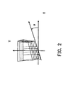
FIG. 2 shows the configuration conformity of the resilient and rugged probe in one embodiment of the invention; and
FIG. 3 shows the contact repeatability vs. frequency graph of measurement result using the resilient and rugged probe provided by the invention;
FIG. 4 shows another embodiment of a resilient and rugged probe of the invention; and
FIG. 5A is a cross sectional view showing a resilient and rugged probe in another embodiment; and
FIG. 5B is a bottom view of the resilient and rugged probe.
DESCRIPTION OF THE PREFERRED EMBODIMENTS
Referring to FIG. 1A, the structure of a resilient and rugged probe in one embodiment is shown. The probe 10 is used to measure the on-wafer signal. In FIG. 1A, the probe 10 includes a metal probe tip 102, a resilient soft multi-layered dielectric substrate 104, a planar transmission structure 106, and a fixed end 108 for supporting the probe 10. The metal probe tip 102 extends outward and suspends from the planar transmission structure into the surrounding air and has a claw shape. The probe tip 102 can move up and down and rotate within a limited range while measuring an uneven or non-planar object. The object can then be probed and measured. The planar transmission structure 106 is coupled to the metal probe tip 102 and attached to the resilient soft multi-layered dielectric substrate 104. The fixed end 108 is coupled to the resilient soft multi-layered dielectric substrate 104 and the planar transmission structure 106 to support and hold the probe 10, and functions as a transmission structure converter of the probe to collect the planar transmission structure 106 and the coaxial transmission structure 120. As shown in FIG. 1C, the coaxial transmission structure 120 is clearly illustrated from the bottom view of the probe 10 and an expanded view of the coaxial transmission structure 120 is shown on the right side. Since the probe 10 is made of metal material and multi-layered soft dielectric material, the far end of the fixed end 108, that is, the metal probe tip 102, allows movement of rotating 110 with an angle φ and diving and lifting 112 with an anile φ, as shown in FIGS. 2 and 4 respectively.
FIG. 2 shows the configuration conformity of a resilient and rugged probe of the invention. The resilience of the probe 10 allows the probe 10 to be bent while probing the signal of the substrate, or example, a microwave signal, and also allows applying pressure to the metal probe tip 102. Such configuration conformity gives the operator great convenience since the object with unevenness to a certain degree can be measured.
Under the same contact state, the resilience of the probe 10 results in the same pressure with any contact angle within a tolerable range, this is the key factor for obtaining the reproducibility of the measurement using the probe 10. Referring to FIG. 3, a contact repeatability vs. frequency graph of a measurement result using the resilient and rugged probe is shown. In FIG. 3, the measurement result is obtained under a non-tilting state, an arbitrary positive tilting angle and an arbitrary negative tilting angle. When the contact reproducibility is −40 dB even when frequency is as high as 26.5 GHz (The error is about 0.3%, which is minor error for microwave network measurement).
FIG. 4 shows the structure of another embodiment of a resilient and rugged probe. FIG. 5A shows the cross-sectional view of the resilient and rugged probe. In FIG. 5A, the probe 50 includes a probe tip 502, a planar transmission structure 504, and a multi-layered dielectric material 506. The probe tip 502 extends outward and freely suspends from the planar transmission structure into the surrounding air and has a claw shape. Since the probe tip 502 is not attached on the dielectric material, the object with an uneven or non-planar structure can be measured by moving the probe up and down and rotating the probe within a limited range. The planar transmission structure 504 is coupled to the probe tip 502, and can be replaced with a connector. The multi-layered dielectric material 506 is coupled to the planar transmission structure 504 and the probe tip 502. Devices 508 could be embedded into the multi-layered dielectric material 506. The device 508, as shown in FIG. 5B, includes a multi-layered microwave circuit 520, a vertical connector 522 or a matching circuit device 524. In this embodiment, the probe 50 can designed as an impedance pre-matching type of probe attached with a bias network to measure the non-system impedance matching device or module. In addition, the probe 50 can be assembled into a mixer type probe to analyze and measure the hybrid chip or device module vector network on the substrate.
Accordingly, the resilient and rugged probe can be used to resolve the problems occurring to the prior art, such as the accuracy and reproducibility problems caused by the evenness of the circuit substrate and the surrounding planarity. In addition, the resilient and rugged probe of the invention is particularly applicable to microwave and high-speed signal measurement. The advantages of the resilient and rugged probe can be concluded as follows.
1. The probe can be bent for configuration conformity.
2. Pressure can be applied to the probe tip by the probe.
3. High measurement reproducibility can be obtained.
4. Operation convenience.
5. Ruggedness.
Other embodiments of the invention will appear to those skilled in the art from consideration of the specification and practice of the invention disclosed herein. It is intended that the specification and examples to be considered as exemplary only, with a true scope and spirit of the invention being indicated by the following claims.

Claims (4)

What is claimed is:
1. A resilient and rugged probe, to measure an on-wafer signal, the probe comprising:
a metal probe tip;
a resilient multi-layered dielectric substrate;
a planar transmission structure, coupled to the metal probe tip and attached onto the resilient multi-layered dielectric substrate, wherein the metal probe tip extends out from the planar transmission structure without being attached to the resilient multi-layered dielectric substrate; and
a fixed end, coupled to the resilient multi-layered dielectric substrate and the planar transmission structure, wherein the fixed end is used as a transmission structure converter of the probe to connect the planar transmission structure to a coaxial transmission structure.
2. The resilient and rugged probe according to claim 1, wherein the metal probe tip is used to probe the on-wafer signal.
3. The resilient and rugged probe according to claim 1, wherein the metal probe tip is able to lift and dive with a second angle.
4. The resilient and rugged probe according to claim 1, wherein the fixed end is used to support and hold the probe.
US10/033,749 2001-12-19 2001-12-19 Resilient and rugged multi-layered probe Expired - Lifetime US6759859B2 (en)

Priority Applications (2)

Application Number Priority Date Filing Date Title
US10/033,749 US6759859B2 (en) 2001-12-19 2001-12-19 Resilient and rugged multi-layered probe
US10/818,958 US6930497B2 (en) 2001-12-19 2004-04-05 Flexible multi-layered probe for measuring a signal from an object

Applications Claiming Priority (1)

Application Number Priority Date Filing Date Title
US10/033,749 US6759859B2 (en) 2001-12-19 2001-12-19 Resilient and rugged multi-layered probe

Related Child Applications (1)

Application Number Title Priority Date Filing Date
US10/818,958 Continuation-In-Part US6930497B2 (en) 2001-12-19 2004-04-05 Flexible multi-layered probe for measuring a signal from an object

Publications (2)

Publication Number Publication Date
US20030112024A1 US20030112024A1 (en) 2003-06-19
US6759859B2 true US6759859B2 (en) 2004-07-06

Family

ID=21872205

Family Applications (1)

Application Number Title Priority Date Filing Date
US10/033,749 Expired - Lifetime US6759859B2 (en) 2001-12-19 2001-12-19 Resilient and rugged multi-layered probe

Country Status (1)

Country Link
US (1) US6759859B2 (en)

Cited By (15)

* Cited by examiner, † Cited by third party
Publication number Priority date Publication date Assignee Title
US20040189334A1 (en) * 2001-12-19 2004-09-30 Deng Joseph D. S. Flexible multi-layered probe
US7420381B2 (en) 2004-09-13 2008-09-02 Cascade Microtech, Inc. Double sided probing structures
US7427868B2 (en) * 2003-12-24 2008-09-23 Cascade Microtech, Inc. Active wafer probe
US7656172B2 (en) 2005-01-31 2010-02-02 Cascade Microtech, Inc. System for testing semiconductors
US7688097B2 (en) 2000-12-04 2010-03-30 Cascade Microtech, Inc. Wafer probe
US7723999B2 (en) 2006-06-12 2010-05-25 Cascade Microtech, Inc. Calibration structures for differential signal probing
US7750652B2 (en) 2006-06-12 2010-07-06 Cascade Microtech, Inc. Test structure and probe for differential signals
US7764072B2 (en) 2006-06-12 2010-07-27 Cascade Microtech, Inc. Differential signal probing system
US7876114B2 (en) 2007-08-08 2011-01-25 Cascade Microtech, Inc. Differential waveguide probe
US7898281B2 (en) 2005-01-31 2011-03-01 Cascade Mircotech, Inc. Interface for testing semiconductors
US7898273B2 (en) 2003-05-23 2011-03-01 Cascade Microtech, Inc. Probe for testing a device under test
WO2012024007A2 (en) 2010-05-21 2012-02-23 University Of Virginia Patent Foundation Micromachined on-wafer probes and related method
US20140028413A1 (en) * 2010-11-29 2014-01-30 Yokowo Co., Ltd. Signal transmission medium and high frequency signal transmission medium
US20210302489A1 (en) * 2017-12-05 2021-09-30 Intel Corporation Multi-member test probe structure
US11822249B2 (en) 2017-12-28 2023-11-21 Intel Corporation Method and apparatus to develop lithographically defined high aspect ratio interconnects

Families Citing this family (1)

* Cited by examiner, † Cited by third party
Publication number Priority date Publication date Assignee Title
WO2015095775A1 (en) * 2013-12-20 2015-06-25 Celadon Systems, Inc. Microelectromechanical system (mems) based probe

Citations (8)

* Cited by examiner, † Cited by third party
Publication number Priority date Publication date Assignee Title
US3596228A (en) * 1969-05-29 1971-07-27 Ibm Fluid actuated contactor
US4697143A (en) 1984-04-30 1987-09-29 Cascade Microtech, Inc. Wafer probe
US4764723A (en) * 1986-11-10 1988-08-16 Cascade Microtech, Inc. Wafer probe
US4827211A (en) * 1987-01-30 1989-05-02 Cascade Microtech, Inc. Wafer probe
US4853627A (en) * 1985-12-23 1989-08-01 Triquint Semiconductor, Inc. Wafer probes
US4998062A (en) * 1988-10-25 1991-03-05 Tokyo Electron Limited Probe device having micro-strip line structure
US5373231A (en) * 1993-06-10 1994-12-13 G. G. B. Industries, Inc. Integrated circuit probing apparatus including a capacitor bypass structure
US5506515A (en) 1994-07-20 1996-04-09 Cascade Microtech, Inc. High-frequency probe tip assembly

Patent Citations (8)

* Cited by examiner, † Cited by third party
Publication number Priority date Publication date Assignee Title
US3596228A (en) * 1969-05-29 1971-07-27 Ibm Fluid actuated contactor
US4697143A (en) 1984-04-30 1987-09-29 Cascade Microtech, Inc. Wafer probe
US4853627A (en) * 1985-12-23 1989-08-01 Triquint Semiconductor, Inc. Wafer probes
US4764723A (en) * 1986-11-10 1988-08-16 Cascade Microtech, Inc. Wafer probe
US4827211A (en) * 1987-01-30 1989-05-02 Cascade Microtech, Inc. Wafer probe
US4998062A (en) * 1988-10-25 1991-03-05 Tokyo Electron Limited Probe device having micro-strip line structure
US5373231A (en) * 1993-06-10 1994-12-13 G. G. B. Industries, Inc. Integrated circuit probing apparatus including a capacitor bypass structure
US5506515A (en) 1994-07-20 1996-04-09 Cascade Microtech, Inc. High-frequency probe tip assembly

Non-Patent Citations (1)

* Cited by examiner, † Cited by third party
Title
"Rugged Probe Design Delivers Mic Measurements" Markku Jenu / VTI Information Technology / Design Feature, Jun. 1995 / p. 104, 106 and 109.

Cited By (23)

* Cited by examiner, † Cited by third party
Publication number Priority date Publication date Assignee Title
US7761983B2 (en) 2000-12-04 2010-07-27 Cascade Microtech, Inc. Method of assembling a wafer probe
US7688097B2 (en) 2000-12-04 2010-03-30 Cascade Microtech, Inc. Wafer probe
US20040189334A1 (en) * 2001-12-19 2004-09-30 Deng Joseph D. S. Flexible multi-layered probe
US6930497B2 (en) * 2001-12-19 2005-08-16 Chung Shan Institute Of Science And Technology Armaments Bureau, M.N.D. Flexible multi-layered probe for measuring a signal from an object
US7898273B2 (en) 2003-05-23 2011-03-01 Cascade Microtech, Inc. Probe for testing a device under test
US7427868B2 (en) * 2003-12-24 2008-09-23 Cascade Microtech, Inc. Active wafer probe
US7759953B2 (en) 2003-12-24 2010-07-20 Cascade Microtech, Inc. Active wafer probe
US7420381B2 (en) 2004-09-13 2008-09-02 Cascade Microtech, Inc. Double sided probing structures
US8013623B2 (en) 2004-09-13 2011-09-06 Cascade Microtech, Inc. Double sided probing structures
US7656172B2 (en) 2005-01-31 2010-02-02 Cascade Microtech, Inc. System for testing semiconductors
US7898281B2 (en) 2005-01-31 2011-03-01 Cascade Mircotech, Inc. Interface for testing semiconductors
US7940069B2 (en) 2005-01-31 2011-05-10 Cascade Microtech, Inc. System for testing semiconductors
US7764072B2 (en) 2006-06-12 2010-07-27 Cascade Microtech, Inc. Differential signal probing system
US7750652B2 (en) 2006-06-12 2010-07-06 Cascade Microtech, Inc. Test structure and probe for differential signals
US7723999B2 (en) 2006-06-12 2010-05-25 Cascade Microtech, Inc. Calibration structures for differential signal probing
US7876114B2 (en) 2007-08-08 2011-01-25 Cascade Microtech, Inc. Differential waveguide probe
WO2012024007A2 (en) 2010-05-21 2012-02-23 University Of Virginia Patent Foundation Micromachined on-wafer probes and related method
US9366697B2 (en) 2010-05-21 2016-06-14 University Of Virginia Patent Foundation Micromachined on-wafer probes and related method
US20140028413A1 (en) * 2010-11-29 2014-01-30 Yokowo Co., Ltd. Signal transmission medium and high frequency signal transmission medium
US9335344B2 (en) * 2010-11-29 2016-05-10 Yokowo Co., Ltd. Signal transmission medium conversion mechanism including a probe tip and a flexible transmission line
US20210302489A1 (en) * 2017-12-05 2021-09-30 Intel Corporation Multi-member test probe structure
US11774489B2 (en) * 2017-12-05 2023-10-03 Intel Corporation Multi-member test probe structure
US11822249B2 (en) 2017-12-28 2023-11-21 Intel Corporation Method and apparatus to develop lithographically defined high aspect ratio interconnects

Also Published As

Publication number Publication date
US20030112024A1 (en) 2003-06-19

Similar Documents

Publication Publication Date Title
US6759859B2 (en) Resilient and rugged multi-layered probe
JP4024324B2 (en) Probe measurement network evaluation system
US7876114B2 (en) Differential waveguide probe
US6343940B1 (en) Contact structure and assembly mechanism thereof
CN107894521B (en) Coaxial probe card device
US6930497B2 (en) Flexible multi-layered probe for measuring a signal from an object
JP2004177400A (en) Interfacing device of probe
TWI705255B (en) Testing device for testing chip
US4829242A (en) Multigigahertz probe
US20020043983A1 (en) Chip-testing socket using surface mount techinology
US7795889B2 (en) Probe device
KR102174427B1 (en) Test Device
WO2003088349A1 (en) Signal detection contactor and signal correcting system
JP2003215164A (en) Elastic durable type probe
TWI623753B (en) Coaxial probe card device
US10429436B2 (en) Method, device and system for measuring an electrical characteristic of a substrate
Rumiantsev et al. Calibration, Repeatability and Related Characteristics of On-wafer, Broadband 70 kHz–220 GHz Single-Sweep Measurements
KR102233780B1 (en) Jig for testing performance of chip set
KR101171959B1 (en) On-Wafer Measurement Device
TWI747750B (en) Calibration structure and calibration method for double-sided probing measurement
US11774491B1 (en) System and method for testing a semiconductor chip
US20220113334A1 (en) Probe card
KR20030004474A (en) Calibrating device for a multilayer laminated circuit module and method for making thereof, and method for measuring high frequency property of the multilayer laminated circuit module by using the calibrating device
JPH0652748B2 (en) Probe card
KR100337234B1 (en) high speed probe for test automation

Legal Events

Date Code Title Description
AS Assignment

Owner name: CHUNG-SHAN INSTITUTE OF SCIENCE AND TECHNOLOGY, TA

Free format text: ASSIGNMENT OF ASSIGNORS INTEREST;ASSIGNORS:DENG, JOSEPH D.S.;LEE, HONG-CHYI;REEL/FRAME:012433/0457

Effective date: 20011205

STCF Information on status: patent grant

Free format text: PATENTED CASE

FPAY Fee payment

Year of fee payment: 4

FPAY Fee payment

Year of fee payment: 8

AS Assignment

Owner name: NATIONAL CHUNG SHAN INSTITUTE OF SCIENCE AND TECHN

Free format text: CHANGE OF NAME;ASSIGNOR:CHUNG-SHAN INSTITUTE OF SCIENCE AND TECHNOLOGY;REEL/FRAME:035453/0240

Effective date: 20140129

FPAY Fee payment

Year of fee payment: 12