US6767474B2 - Fluid ejector head having a planar passivation layer - Google Patents
Fluid ejector head having a planar passivation layer Download PDFInfo
- Publication number
- US6767474B2 US6767474B2 US10/198,904 US19890402A US6767474B2 US 6767474 B2 US6767474 B2 US 6767474B2 US 19890402 A US19890402 A US 19890402A US 6767474 B2 US6767474 B2 US 6767474B2
- Authority
- US
- United States
- Prior art keywords
- layer
- forming
- fluid
- chamber
- accordance
- Prior art date
- Legal status (The legal status is an assumption and is not a legal conclusion. Google has not performed a legal analysis and makes no representation as to the accuracy of the status listed.)
- Expired - Fee Related
Links
- 239000012530 fluid Substances 0.000 title claims abstract description 181
- 238000002161 passivation Methods 0.000 title claims abstract description 50
- 239000000463 material Substances 0.000 claims abstract description 55
- 238000011049 filling Methods 0.000 claims abstract description 6
- 238000000034 method Methods 0.000 claims description 41
- 239000000758 substrate Substances 0.000 claims description 37
- XUIMIQQOPSSXEZ-UHFFFAOYSA-N Silicon Chemical compound [Si] XUIMIQQOPSSXEZ-UHFFFAOYSA-N 0.000 claims description 16
- 229910052710 silicon Inorganic materials 0.000 claims description 15
- 239000010703 silicon Substances 0.000 claims description 15
- 238000004519 manufacturing process Methods 0.000 claims description 7
- 238000000926 separation method Methods 0.000 claims description 7
- 229910052581 Si3N4 Inorganic materials 0.000 claims description 6
- 238000005530 etching Methods 0.000 claims description 5
- HBMJWWWQQXIZIP-UHFFFAOYSA-N silicon carbide Chemical compound [Si+]#[C-] HBMJWWWQQXIZIP-UHFFFAOYSA-N 0.000 claims description 5
- 229910010271 silicon carbide Inorganic materials 0.000 claims description 5
- HQVNEWCFYHHQES-UHFFFAOYSA-N silicon nitride Chemical compound N12[Si]34N5[Si]62N3[Si]51N64 HQVNEWCFYHHQES-UHFFFAOYSA-N 0.000 claims description 5
- 238000005468 ion implantation Methods 0.000 claims description 4
- 238000001053 micromoulding Methods 0.000 claims description 3
- 238000005498 polishing Methods 0.000 claims description 2
- 239000000126 substance Substances 0.000 claims description 2
- 229910052715 tantalum Inorganic materials 0.000 claims description 2
- GUVRBAGPIYLISA-UHFFFAOYSA-N tantalum atom Chemical compound [Ta] GUVRBAGPIYLISA-UHFFFAOYSA-N 0.000 claims description 2
- 238000001312 dry etching Methods 0.000 claims 1
- 238000001039 wet etching Methods 0.000 claims 1
- 239000010410 layer Substances 0.000 description 140
- 239000000976 ink Substances 0.000 description 15
- VYPSYNLAJGMNEJ-UHFFFAOYSA-N Silicium dioxide Chemical compound O=[Si]=O VYPSYNLAJGMNEJ-UHFFFAOYSA-N 0.000 description 12
- 229910052751 metal Inorganic materials 0.000 description 11
- 239000002184 metal Substances 0.000 description 11
- 239000004020 conductor Substances 0.000 description 9
- 229920001721 polyimide Polymers 0.000 description 9
- 238000003860 storage Methods 0.000 description 9
- 229910052814 silicon oxide Inorganic materials 0.000 description 8
- 239000004642 Polyimide Substances 0.000 description 6
- 230000007613 environmental effect Effects 0.000 description 5
- 230000015556 catabolic process Effects 0.000 description 4
- 238000005229 chemical vapour deposition Methods 0.000 description 4
- 238000006731 degradation reaction Methods 0.000 description 4
- 239000003989 dielectric material Substances 0.000 description 4
- 230000007246 mechanism Effects 0.000 description 4
- 229920000642 polymer Polymers 0.000 description 4
- 239000004065 semiconductor Substances 0.000 description 4
- WGTYBPLFGIVFAS-UHFFFAOYSA-M tetramethylammonium hydroxide Chemical compound [OH-].C[N+](C)(C)C WGTYBPLFGIVFAS-UHFFFAOYSA-M 0.000 description 4
- HEMHJVSKTPXQMS-UHFFFAOYSA-M Sodium hydroxide Chemical compound [OH-].[Na+] HEMHJVSKTPXQMS-UHFFFAOYSA-M 0.000 description 3
- 238000000151 deposition Methods 0.000 description 3
- 238000000608 laser ablation Methods 0.000 description 3
- 150000002739 metals Chemical class 0.000 description 3
- 238000000206 photolithography Methods 0.000 description 3
- 238000007639 printing Methods 0.000 description 3
- 238000004544 sputter deposition Methods 0.000 description 3
- 229910000838 Al alloy Inorganic materials 0.000 description 2
- NLXLAEXVIDQMFP-UHFFFAOYSA-N Ammonia chloride Chemical compound [NH4+].[Cl-] NLXLAEXVIDQMFP-UHFFFAOYSA-N 0.000 description 2
- 239000004593 Epoxy Substances 0.000 description 2
- KRHYYFGTRYWZRS-UHFFFAOYSA-N Fluorane Chemical compound F KRHYYFGTRYWZRS-UHFFFAOYSA-N 0.000 description 2
- 238000009835 boiling Methods 0.000 description 2
- 230000003247 decreasing effect Effects 0.000 description 2
- 230000008021 deposition Effects 0.000 description 2
- 238000005323 electroforming Methods 0.000 description 2
- 239000011521 glass Substances 0.000 description 2
- 239000000377 silicon dioxide Substances 0.000 description 2
- 235000012239 silicon dioxide Nutrition 0.000 description 2
- 229910000679 solder Inorganic materials 0.000 description 2
- JBRZTFJDHDCESZ-UHFFFAOYSA-N AsGa Chemical compound [As]#[Ga] JBRZTFJDHDCESZ-UHFFFAOYSA-N 0.000 description 1
- 229910052582 BN Inorganic materials 0.000 description 1
- PZNSFCLAULLKQX-UHFFFAOYSA-N Boron nitride Chemical compound N#B PZNSFCLAULLKQX-UHFFFAOYSA-N 0.000 description 1
- RYGMFSIKBFXOCR-UHFFFAOYSA-N Copper Chemical compound [Cu] RYGMFSIKBFXOCR-UHFFFAOYSA-N 0.000 description 1
- 229910001218 Gallium arsenide Inorganic materials 0.000 description 1
- OAICVXFJPJFONN-UHFFFAOYSA-N Phosphorus Chemical group [P] OAICVXFJPJFONN-UHFFFAOYSA-N 0.000 description 1
- 229910000676 Si alloy Inorganic materials 0.000 description 1
- 229910004012 SiCx Inorganic materials 0.000 description 1
- 229910020776 SixNy Inorganic materials 0.000 description 1
- 230000003213 activating effect Effects 0.000 description 1
- 239000000654 additive Substances 0.000 description 1
- 230000000996 additive effect Effects 0.000 description 1
- 229910045601 alloy Inorganic materials 0.000 description 1
- 239000000956 alloy Substances 0.000 description 1
- RVSGESPTHDDNTH-UHFFFAOYSA-N alumane;tantalum Chemical compound [AlH3].[Ta] RVSGESPTHDDNTH-UHFFFAOYSA-N 0.000 description 1
- 229910052782 aluminium Inorganic materials 0.000 description 1
- XAGFODPZIPBFFR-UHFFFAOYSA-N aluminium Chemical compound [Al] XAGFODPZIPBFFR-UHFFFAOYSA-N 0.000 description 1
- -1 aluminum copper silicon Chemical compound 0.000 description 1
- 235000019270 ammonium chloride Nutrition 0.000 description 1
- 239000011324 bead Substances 0.000 description 1
- 238000003486 chemical etching Methods 0.000 description 1
- 229910052802 copper Inorganic materials 0.000 description 1
- 239000010949 copper Substances 0.000 description 1
- 230000008878 coupling Effects 0.000 description 1
- 238000010168 coupling process Methods 0.000 description 1
- 238000005859 coupling reaction Methods 0.000 description 1
- 229910021419 crystalline silicon Inorganic materials 0.000 description 1
- 238000004090 dissolution Methods 0.000 description 1
- 238000005566 electron beam evaporation Methods 0.000 description 1
- 238000009713 electroplating Methods 0.000 description 1
- 238000005538 encapsulation Methods 0.000 description 1
- 238000005516 engineering process Methods 0.000 description 1
- 230000001747 exhibiting effect Effects 0.000 description 1
- 238000010304 firing Methods 0.000 description 1
- 230000004927 fusion Effects 0.000 description 1
- PCHJSUWPFVWCPO-UHFFFAOYSA-N gold Chemical compound [Au] PCHJSUWPFVWCPO-UHFFFAOYSA-N 0.000 description 1
- 229910052737 gold Inorganic materials 0.000 description 1
- 239000010931 gold Substances 0.000 description 1
- 238000000227 grinding Methods 0.000 description 1
- GPRLSGONYQIRFK-UHFFFAOYSA-N hydron Chemical compound [H+] GPRLSGONYQIRFK-UHFFFAOYSA-N 0.000 description 1
- 238000007641 inkjet printing Methods 0.000 description 1
- 239000011147 inorganic material Substances 0.000 description 1
- 238000002527 ion beam patterning Methods 0.000 description 1
- 238000002955 isolation Methods 0.000 description 1
- 238000003475 lamination Methods 0.000 description 1
- 230000000873 masking effect Effects 0.000 description 1
- 239000011159 matrix material Substances 0.000 description 1
- 238000010297 mechanical methods and process Methods 0.000 description 1
- 239000012528 membrane Substances 0.000 description 1
- 238000003801 milling Methods 0.000 description 1
- 239000002991 molded plastic Substances 0.000 description 1
- 229910021421 monocrystalline silicon Inorganic materials 0.000 description 1
- 239000011368 organic material Substances 0.000 description 1
- TWNQGVIAIRXVLR-UHFFFAOYSA-N oxo(oxoalumanyloxy)alumane Chemical compound O=[Al]O[Al]=O TWNQGVIAIRXVLR-UHFFFAOYSA-N 0.000 description 1
- 238000000059 patterning Methods 0.000 description 1
- 150000002978 peroxides Chemical class 0.000 description 1
- 229910052698 phosphorus Inorganic materials 0.000 description 1
- 239000011574 phosphorus Substances 0.000 description 1
- 229920002120 photoresistant polymer Polymers 0.000 description 1
- 238000001020 plasma etching Methods 0.000 description 1
- 238000000623 plasma-assisted chemical vapour deposition Methods 0.000 description 1
- 229910021420 polycrystalline silicon Inorganic materials 0.000 description 1
- 229920006254 polymer film Polymers 0.000 description 1
- 229920005591 polysilicon Polymers 0.000 description 1
- 238000002360 preparation method Methods 0.000 description 1
- 239000011241 protective layer Substances 0.000 description 1
- 238000004080 punching Methods 0.000 description 1
- WNUPENMBHHEARK-UHFFFAOYSA-N silicon tungsten Chemical compound [Si].[W] WNUPENMBHHEARK-UHFFFAOYSA-N 0.000 description 1
- 238000004528 spin coating Methods 0.000 description 1
- 238000000992 sputter etching Methods 0.000 description 1
- 238000002207 thermal evaporation Methods 0.000 description 1
Images


Classifications
-
- B—PERFORMING OPERATIONS; TRANSPORTING
- B41—PRINTING; LINING MACHINES; TYPEWRITERS; STAMPS
- B41J—TYPEWRITERS; SELECTIVE PRINTING MECHANISMS, i.e. MECHANISMS PRINTING OTHERWISE THAN FROM A FORME; CORRECTION OF TYPOGRAPHICAL ERRORS
- B41J2/00—Typewriters or selective printing mechanisms characterised by the printing or marking process for which they are designed
- B41J2/005—Typewriters or selective printing mechanisms characterised by the printing or marking process for which they are designed characterised by bringing liquid or particles selectively into contact with a printing material
- B41J2/01—Ink jet
- B41J2/135—Nozzles
- B41J2/16—Production of nozzles
- B41J2/1621—Manufacturing processes
- B41J2/1626—Manufacturing processes etching
- B41J2/1629—Manufacturing processes etching wet etching
-
- B—PERFORMING OPERATIONS; TRANSPORTING
- B41—PRINTING; LINING MACHINES; TYPEWRITERS; STAMPS
- B41J—TYPEWRITERS; SELECTIVE PRINTING MECHANISMS, i.e. MECHANISMS PRINTING OTHERWISE THAN FROM A FORME; CORRECTION OF TYPOGRAPHICAL ERRORS
- B41J2/00—Typewriters or selective printing mechanisms characterised by the printing or marking process for which they are designed
- B41J2/005—Typewriters or selective printing mechanisms characterised by the printing or marking process for which they are designed characterised by bringing liquid or particles selectively into contact with a printing material
- B41J2/01—Ink jet
- B41J2/135—Nozzles
- B41J2/16—Production of nozzles
- B41J2/1601—Production of bubble jet print heads
- B41J2/1603—Production of bubble jet print heads of the front shooter type
-
- B—PERFORMING OPERATIONS; TRANSPORTING
- B41—PRINTING; LINING MACHINES; TYPEWRITERS; STAMPS
- B41J—TYPEWRITERS; SELECTIVE PRINTING MECHANISMS, i.e. MECHANISMS PRINTING OTHERWISE THAN FROM A FORME; CORRECTION OF TYPOGRAPHICAL ERRORS
- B41J2/00—Typewriters or selective printing mechanisms characterised by the printing or marking process for which they are designed
- B41J2/005—Typewriters or selective printing mechanisms characterised by the printing or marking process for which they are designed characterised by bringing liquid or particles selectively into contact with a printing material
- B41J2/01—Ink jet
- B41J2/135—Nozzles
- B41J2/16—Production of nozzles
- B41J2/1621—Manufacturing processes
- B41J2/1623—Manufacturing processes bonding and adhesion
-
- B—PERFORMING OPERATIONS; TRANSPORTING
- B41—PRINTING; LINING MACHINES; TYPEWRITERS; STAMPS
- B41J—TYPEWRITERS; SELECTIVE PRINTING MECHANISMS, i.e. MECHANISMS PRINTING OTHERWISE THAN FROM A FORME; CORRECTION OF TYPOGRAPHICAL ERRORS
- B41J2/00—Typewriters or selective printing mechanisms characterised by the printing or marking process for which they are designed
- B41J2/005—Typewriters or selective printing mechanisms characterised by the printing or marking process for which they are designed characterised by bringing liquid or particles selectively into contact with a printing material
- B41J2/01—Ink jet
- B41J2/135—Nozzles
- B41J2/16—Production of nozzles
- B41J2/1621—Manufacturing processes
- B41J2/1625—Manufacturing processes electroforming
-
- B—PERFORMING OPERATIONS; TRANSPORTING
- B41—PRINTING; LINING MACHINES; TYPEWRITERS; STAMPS
- B41J—TYPEWRITERS; SELECTIVE PRINTING MECHANISMS, i.e. MECHANISMS PRINTING OTHERWISE THAN FROM A FORME; CORRECTION OF TYPOGRAPHICAL ERRORS
- B41J2/00—Typewriters or selective printing mechanisms characterised by the printing or marking process for which they are designed
- B41J2/005—Typewriters or selective printing mechanisms characterised by the printing or marking process for which they are designed characterised by bringing liquid or particles selectively into contact with a printing material
- B41J2/01—Ink jet
- B41J2/135—Nozzles
- B41J2/16—Production of nozzles
- B41J2/1621—Manufacturing processes
- B41J2/1626—Manufacturing processes etching
- B41J2/1628—Manufacturing processes etching dry etching
-
- B—PERFORMING OPERATIONS; TRANSPORTING
- B41—PRINTING; LINING MACHINES; TYPEWRITERS; STAMPS
- B41J—TYPEWRITERS; SELECTIVE PRINTING MECHANISMS, i.e. MECHANISMS PRINTING OTHERWISE THAN FROM A FORME; CORRECTION OF TYPOGRAPHICAL ERRORS
- B41J2/00—Typewriters or selective printing mechanisms characterised by the printing or marking process for which they are designed
- B41J2/005—Typewriters or selective printing mechanisms characterised by the printing or marking process for which they are designed characterised by bringing liquid or particles selectively into contact with a printing material
- B41J2/01—Ink jet
- B41J2/135—Nozzles
- B41J2/16—Production of nozzles
- B41J2/1621—Manufacturing processes
- B41J2/1632—Manufacturing processes machining
-
- B—PERFORMING OPERATIONS; TRANSPORTING
- B41—PRINTING; LINING MACHINES; TYPEWRITERS; STAMPS
- B41J—TYPEWRITERS; SELECTIVE PRINTING MECHANISMS, i.e. MECHANISMS PRINTING OTHERWISE THAN FROM A FORME; CORRECTION OF TYPOGRAPHICAL ERRORS
- B41J2/00—Typewriters or selective printing mechanisms characterised by the printing or marking process for which they are designed
- B41J2/005—Typewriters or selective printing mechanisms characterised by the printing or marking process for which they are designed characterised by bringing liquid or particles selectively into contact with a printing material
- B41J2/01—Ink jet
- B41J2/135—Nozzles
- B41J2/16—Production of nozzles
- B41J2/1621—Manufacturing processes
- B41J2/1637—Manufacturing processes molding
- B41J2/1639—Manufacturing processes molding sacrificial molding
-
- B—PERFORMING OPERATIONS; TRANSPORTING
- B41—PRINTING; LINING MACHINES; TYPEWRITERS; STAMPS
- B41J—TYPEWRITERS; SELECTIVE PRINTING MECHANISMS, i.e. MECHANISMS PRINTING OTHERWISE THAN FROM A FORME; CORRECTION OF TYPOGRAPHICAL ERRORS
- B41J2/00—Typewriters or selective printing mechanisms characterised by the printing or marking process for which they are designed
- B41J2/005—Typewriters or selective printing mechanisms characterised by the printing or marking process for which they are designed characterised by bringing liquid or particles selectively into contact with a printing material
- B41J2/01—Ink jet
- B41J2/135—Nozzles
- B41J2/16—Production of nozzles
- B41J2/1621—Manufacturing processes
- B41J2/164—Manufacturing processes thin film formation
- B41J2/1642—Manufacturing processes thin film formation thin film formation by CVD [chemical vapor deposition]
-
- B—PERFORMING OPERATIONS; TRANSPORTING
- B41—PRINTING; LINING MACHINES; TYPEWRITERS; STAMPS
- B41J—TYPEWRITERS; SELECTIVE PRINTING MECHANISMS, i.e. MECHANISMS PRINTING OTHERWISE THAN FROM A FORME; CORRECTION OF TYPOGRAPHICAL ERRORS
- B41J2/00—Typewriters or selective printing mechanisms characterised by the printing or marking process for which they are designed
- B41J2/005—Typewriters or selective printing mechanisms characterised by the printing or marking process for which they are designed characterised by bringing liquid or particles selectively into contact with a printing material
- B41J2/01—Ink jet
- B41J2/135—Nozzles
- B41J2/16—Production of nozzles
- B41J2/1621—Manufacturing processes
- B41J2/164—Manufacturing processes thin film formation
- B41J2/1643—Manufacturing processes thin film formation thin film formation by plating
-
- B—PERFORMING OPERATIONS; TRANSPORTING
- B41—PRINTING; LINING MACHINES; TYPEWRITERS; STAMPS
- B41J—TYPEWRITERS; SELECTIVE PRINTING MECHANISMS, i.e. MECHANISMS PRINTING OTHERWISE THAN FROM A FORME; CORRECTION OF TYPOGRAPHICAL ERRORS
- B41J2/00—Typewriters or selective printing mechanisms characterised by the printing or marking process for which they are designed
- B41J2/005—Typewriters or selective printing mechanisms characterised by the printing or marking process for which they are designed characterised by bringing liquid or particles selectively into contact with a printing material
- B41J2/01—Ink jet
- B41J2/135—Nozzles
- B41J2/16—Production of nozzles
- B41J2/1621—Manufacturing processes
- B41J2/164—Manufacturing processes thin film formation
- B41J2/1645—Manufacturing processes thin film formation thin film formation by spincoating
-
- B—PERFORMING OPERATIONS; TRANSPORTING
- B41—PRINTING; LINING MACHINES; TYPEWRITERS; STAMPS
- B41J—TYPEWRITERS; SELECTIVE PRINTING MECHANISMS, i.e. MECHANISMS PRINTING OTHERWISE THAN FROM A FORME; CORRECTION OF TYPOGRAPHICAL ERRORS
- B41J2/00—Typewriters or selective printing mechanisms characterised by the printing or marking process for which they are designed
- B41J2/005—Typewriters or selective printing mechanisms characterised by the printing or marking process for which they are designed characterised by bringing liquid or particles selectively into contact with a printing material
- B41J2/01—Ink jet
- B41J2/135—Nozzles
- B41J2/16—Production of nozzles
- B41J2/1621—Manufacturing processes
- B41J2/164—Manufacturing processes thin film formation
- B41J2/1646—Manufacturing processes thin film formation thin film formation by sputtering
Definitions
- Fluid ejection cartridges typically include a fluid reservoir that is fluidically coupled to a substrate.
- the substrate normally contains an energy-generating element that generates the force necessary for ejecting the fluid through one or more nozzles.
- Two widely used energy-generating elements are thermal resistors and piezoelectric elements. The former rapidly heats a component in the fluid above its boiling point creating a bubble causing ejection of a drop of the fluid. The latter utilizes a voltage pulse to move a membrane that displaces the fluid resulting in ejection of a drop of the fluid.
- Improvements in image quality have typically led to an increase in the organic content of inkjet inks.
- This increase in organic content typically leads to inks exhibiting a more corrosive nature, potentially resulting in the degradation of the materials coming into contact with such inks.
- Degradation of these materials by more corrosive inks raises reliability and material compatibility issues.
- These material compatibility issues generally relate to all the materials the ink comes in contact with. However, they are exacerbated in the printhead because, in an off-axis system, the materials around the fluid ejectors and nozzles need to maintain their functionality over a longer period of time. This increased reliability is necessary to ensure continued proper functioning of the printhead, at least through several replacements of the ink cartridges. Thus, degradation of these materials can lead to potentially catastrophic failures of the printhead.
- Improvements in image quality have also typically resulted in demand for printheads with fluid ejector heads capable of ejecting smaller fluid drops. Generally, this is accomplished by decreasing the size of the resistor as well as decreasing the size and thickness of the fluid chamber surrounding the resistor. In addition, the size and thickness of the orifice or bore, through which the fluid is ejected, is also typically reduced to eject smaller drops.
- a fluid ejector head is typically fabricated utilizing conventional semiconductor processing equipment. Typically, etching or removing a conductor material creating an area of higher resistance forms the thermal resistor.
- a dielectric passivation layer is then typically deposited over the conductors and the resistor to provide electrical isolation and environmental protection from degradation by the fluid located in the fluid chamber. As the resistors and chambers become smaller the ability to maintain thickness uniformity in the various layers, because of step coverage issues, becomes more difficult. All of these problems can impact the manufacture of lower cost, smaller, and more reliable printer cartridges and printing systems.
- FIG. 1 is a cross-sectional view of a fluid ejector head according to an embodiment of the present invention
- FIG. 2 is a cross-sectional isometric view of a fluid ejector head according to an alternate embodiment of the present invention
- FIG. 3 a is a cross-sectional isometric view of a fluid definition layer of a fluid ejector head according to an embodiment of the present invention
- FIG. 3 b is a cross-sectional isometric view of the fluid definition layer of a fluid ejector head seen in FIG. 3 a after further processing according to an embodiment of the present invention
- FIG. 3 c is a cross-sectional isometric view of the fluid ejector head seen in FIG. 3 b after further processing according to an embodiment of the present invention
- FIG. 3 d is a cross-sectional isometric view of the fluid ejector head seen in FIG. 3 c after further processing according to an embodiment of the present invention
- FIG. 3 e is a cross-sectional isometric view of the fluid ejector head seen in FIG. 3 d after further processing according to an embodiment of the present invention
- FIG. 3 f is a cross-sectional isometric view of the fluid ejector head seen in FIG. 3 e after further processing according to an embodiment of the present invention
- FIG. 3 g is a cross-sectional isometric view of the fluid ejector head seen in FIG. 3 f after further processing according to an embodiment of the present invention
- FIG. 3 h is a cross-sectional isometric view of the fluid ejector head seen in FIG. 3 g after further processing according to an embodiment of the present invention
- FIG. 4 a is a is a cross-sectional isometric view of a silicon wafer according to an embodiment of the present invention.
- FIG. 4 b is a cross-sectional isometric view of a silicon fluid definition layer of a fluid ejector head seen in FIG. 4 a after further processing according to an embodiment of the present invention
- FIG. 4 c is a cross-sectional isometric view of the fluid ejector head seen in FIG. 4 b after further processing according to an embodiment of the present invention
- FIG. 4 d is a cross-sectional isometric view of the fluid ejector head seen in FIG. 4 c after further processing according to an embodiment of the present invention
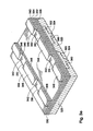
- FIG. 5 is a perspective view of a fluid ejection cartridge according to an embodiment of the present invention.
- FIG. 6 is a perspective view of a fluid ejection system according to an embodiment of the present invention.
- fluid ejector head 100 includes passivation layer 130 , having substantially planar opposed major surfaces. Passivation layer 130 provides environmental, mechanical, and electrical protection to resistor 142 .
- Fluid definition layer 120 includes chamber 122 and bore 124 , which extends from chamber surface 123 to exit surface 125 . Chamber 122 and bore 124 , in this embodiment, are filled with sacrificial material 160 which is planarized to form substantially planar passivation surface 128 on fluid definition layer 120 .
- Passivation layer 130 is formed or deposited on passivation surface 128 formed on fluid definition layer 120 and sacrificial material 160 .
- fluid definition layer 120 is silicon, however, in alternate embodiments, metals, inorganic dielectrics, and various polymers may also be utilized.
- fluid definition layer 120 may be an electrochemically formed metal orifice plate containing bore 124 and chamber 122 .
- fluid definition layer 120 is a micro-molded plastic structure containing chamber 122 and bore 124 .
- polymer layer such as a polyimide film, containing chamber 122 and bore 123 formed by chemically etching or laser ablation.
- Fluid definition layer 120 in this embodiment, has a thickness in the range from about 0.1 micrometers to about 10 micrometers. In alternate embodiments, fluid definition layer 120 may have a thickness in the range from about 0.25 micrometers to about 4.0 micrometers.
- Chamber 122 in this embodiment, has an area in the plane formed by chamber surface 123 in the range from about 0.5 square micrometers to about 10,000 square micrometers.
- bore 124 has an area in the plane formed by exit surface 125 that is less than the area of bore 124 in the plane formed by chamber surface 124 .
- Passivation layer 130 is a dielectric material, such as silicon carbide (SiC x ), silicon nitride (Si x N y ), silicon oxide (SiO x ), boron nitride (BN x ), or a polyimide to name a few.
- passivation layer 130 has a thickness in the range from about 5.0 nanometers to about 200 nanometers. In alternate embodiments, passivation layer 130 may have a thickness in the range from about 5.0 nanometers to about 75 nanometers.
- Resistive layer 140 having substantially planar opposed major surfaces, is disposed over passivation layer 130 forming resistor 142 .
- fluid ejector actuator 110 is thermal resistor 142 that utilizes a voltage pulse to rapidly heat a component in a fluid above its boiling point creating a bubble causing ejection of a drop of the fluid.
- other fluid ejector generators such as piezoelectric, ultrasonic, or electrostatic generators may also be utilized.
- Resistive layer 140 in this embodiment, has a thickness in the range from about 20 nanometers to about 400 nanometers. In alternate embodiments, resistive layer 140 may have a thickness in the range from about 50 nanometers to about 250 nanometers.
- Thermal resistor 142 in this embodiment, has an area in the range from about 0.05 square micrometers to about 2,500 square micrometers. In particular resistors having an area in the range from about 0.25 square micrometers to about 900 square micrometers may be utilized. Electrical conductors 146 including beveled edges 148 are disposed over resistive layer 140 . Beveled edges 148 provide improved step coverage for substrate insulating layer 154 . Electrical conductors 146 have a thickness in the range from about 50 nanometers to about 500 nanometers.
- substrate insulating layer 154 is a silicon oxide layer. However, in alternate embodiments, other materials may also be utilized, such as metals or polymers, depending on the particular substrate material used and the particular application in which fluid ejector head 100 will be used. Substrate insulating layer 154 has a thickness in the range from about 0.20 micrometers to about 2 micrometers. In particular thicknesses in the range from about 0.40 micrometers to about 0.75 micrometers can be utilized. In addition, fluid inlet channels (not shown) are formed in fluid ejector head 100 to provide a fluid path between a reservoir (not shown) and fluid ejector actuator 110 . In this embodiment, substrate 150 is a silicon wafer having a thickness of about 300-700 micrometers.
- substrate 150 may also be utilized for substrate 150 , such as, various glasses, aluminum oxide, polyimide substrates, silicon carbide, and gallium arsenide. Accordingly, the present invention is not intended to be limited to those fluid ejector heads fabricated in silicon semiconductor materials.
- Fluid ejector head 100 described in the present invention can reproducibly and reliably eject drops in the range of from about one femtoliter to about ten nanoliters depending on the parameters and structures of the fluid ejector head such as the size and geometry of the chamber around the fluid ejector, the size and geometry of the fluid ejector, and the size and geometry of the nozzle.
- fluid ejector actuator 110 When fluid ejector actuator 110 is activated the fluid ejector head ejects essentially a drop of a fluid.
- a tail and smaller satellite drops may be formed during the ejection process and are included in volume ejected.
- fluid definition layer 220 is a thick silicon oxide layer formed on bore support or support 218 , which is a silicon wafer.
- fluid definition layer 220 and support 218 may be formed for example from metals, inorganic dielectrics, polymers and combinations thereof.
- Chamber 222 and bore 224 are formed in fluid definition layer 220 .
- chamber 222 may be formed in a layer distinct from the layer that forms bore 224 .
- bore 224 may be formed in an electroformed metal layer with chamber 222 formed in an epoxy layer coated on the electroformed metal layer.
- Another example would be forming bore 224 in a polyimide film and then forming chamber 222 in a silicon dioxide or metal layer deposited on the polyimide film.
- alternate embodiments may have multiple bores formed in fluid definition layer 220 over chamber 222 .
- Passivation layer 230 includes first dielectric layer 232 and second dielectric layer 234 .
- first dielectric layer 232 is silicon carbide and second dielectric layer 234 is silicon nitride.
- Resistive layer 240 , resistor 242 , electrical conductors 246 , and substrate insulating layer 254 are similar to that described above and shown in FIG. 1 .
- Substrate 250 in this embodiment is a metal layer that provides environmental protection as well as thermal dissipation of heat generated when fluid ejector actuators 210 are activated.
- Fluid inlet channels 252 are formed in fluid ejector head 200 to provide a fluid path between a reservoir (not shown) and fluid ejector actuator 210 .
- FIGS. 3 a - 3 h cross-sectional isometric views of a method of manufacturing a fluid ejector head according to an embodiment of the present invention is shown.
- FIG. 3 a shows fluid definition layer 320 , which depending on the particular material utilized may have a support layer (See FIG. 2 ), which will be described in greater detail later.
- FIG. 3 b shows chambers 322 and bores 324 formed in fluid definition layer 320 , where bores 324 extend from chamber surface 323 to exit surface 325 . The process of forming chamber 322 and bore 324 depends on the particular material chosen to form fluid definition layer 320 .
- fluid definition layer 320 is a single crystal silicon layer.
- Chambers 322 and bores 324 are formed by masking fluid definition layer 320 with the appropriate mask and removing the material in the chambers and bores via either a wet or dry etch chemistry.
- a dry etch may be used when vertical or orthogonal sidewalls are desired.
- a wet etch such as tetra methyl ammonium hydroxide (TMAH) when sloping sidewalls are desired.
- TMAH tetra methyl ammonium hydroxide
- combinations of wet and dry etch may also be utilized when more complex structures are utilized for the chamber and bore.
- Other processes such as laser ablation, reactive ion etching, ion milling including focused ion beam patterning may also be utilized to form chambers 322 and bores 324 .
- silicon oxide or silicon nitride may also be utilized, using deposition tools such as sputtering or chemical vapor deposition and photolithography tools for patterning.
- deposition tools such as sputtering or chemical vapor deposition and photolithography tools for patterning.
- Micromolding, electroforming, punching, or chemical milling are all examples of techniques that may also be utilized depending on the particular materials utilized for fluid definition layer 320 .
- the chamber layer defines the sidewalls of the chamber and the orifice layer defines the bore and forms the top of the chamber.
- the processes used to form a photoimagable polyimide orifice layer would be spin coating the polyimide on a bore support layer such as a silicon or metal wafer, followed by soft baking, expose, develop, and subsequently a final bake process.
- a chamber layer can then be formed utilizing the same or a similar polyimide as that used to form the bore.
- the chamber layer may also be formed utilizing a different material such as photoimagable epoxy. Another example would be utilizing what is generally referred to as a solder mask, to form either the chamber or bore, or both.
- a solder mask utilizes a lamination process to adhere the material to a bore support layer, and the remaining steps would be those typically utilized in photolithography.
- a further example would be to form the bore layer by electroforming techniques and then spin coat or laminate a chamber layer material on the bore layer.
- different techniques for creating the bore and chamber may also be utilized such as laser ablation to form the nozzle and photolithographically forming the chamber.
- FIG. 3 c shows planarized sacrificial layer or “lost wax” 360 suitably filling chambers 322 and bores 324 .
- sacrificial layer is a phosphorus doped spin on glass (SOG) spin coated onto fluid definition layer 320 after chambers 322 and bores 324 have been formed.
- Sacrificial material 360 is planarized, for example, by mechanical, resist etch-back, or chemical-mechanical processes, to form substantially planar passivation surface 328 .
- Sacrificial material 360 may be any material that is differentially etchable to the surrounding structures such as the chamber and bore.
- Passivation layer 330 , resistive layer 340 and electrically conductive layer 345 are all formed over passivation surface 328 as shown in FIG. 3 d .
- passivation layer 330 includes cavitation layer 336 , first dielectric layer 332 and second dielectric layer 334 .
- Cavitation layer 336 in this embodiment, is a tantalum layer, however, in other embodiments cavitation layer may be any inorganic or organic material that has the appropriate environmental, crack and fatigue resistant properties, depending on the particular application in which the fluid ejector head will be used.
- First dielectric layer 332 and second dielectric layer 334 in this embodiment, are a silicon carbide layer, and a silicon nitride layer respectively.
- cavitation layer 336 , first dielectric layer 332 , and second dielectric layer 334 have a thickness in the range from about 2.5 nanometers to about 200 nanometers.
- Resistive layer 340 in this embodiment, is a tantalum aluminum alloy. In alternate embodiments, resistor alloys such as tungsten silicon nitride, or polysilicon may also be utilized. In other alternative embodiments, fluid drop actuators other than thermal resistors, such as piezoelectric, or ultrasonic may also be utilized. Electrically conductive layer 345 , in this embodiment, is an aluminum copper silicon alloy. In other alternative embodiments, other interconnect materials commonly used in integrated circuit or printed circuit board technologies, such as other aluminum alloys, gold, or copper, may be utilized to form electrically conductive layer 345 .
- the process of creating passivation layer 330 , resistive 340 , and electrically conductive layer 345 utilizes conventional semiconductor processing equipment, such as sputter deposition systems, or chemical vapor deposition (CVD) systems for forming the layers.
- conventional semiconductor processing equipment such as sputter deposition systems, or chemical vapor deposition (CVD) systems for forming the layers.
- CVD chemical vapor deposition
- other techniques such as electron beam or thermal evaporation, plasma enhanced CVD, electroplating, or electroless deposition, may also be utilized separately or in combination with sputter deposition or CVD to form the layers depending on the particular materials utilized.
- Resistors 342 and electrical conductors 346 are formed utilizing conventional semiconductor or printed circuit board processing equipment.
- a subtractive process is used for defining or etching the location and shape of resistors 342 and electrical conductors or traces 346 as shown in FIG. 3 e .
- a subtractive process is shown an additive process, where material is selectively deposited rather than removed, may also be utilized to form resistors 342 and electrical traces 346 .
- a slope metal etch may also be utilized in forming electrical conductors 346 to provide better step coverage for depositing or forming substrate insulating layer 354 as shown in FIG. 3 f .
- Substrate insulating layer 354 serves to electrically isolate electrical conductors 346 and resistors 342 when an electrically conductive substrate such as silicon or a metal is utilized. In addition substrate insulating layer 354 also provides mechanical and environmental protection of resistors 342 . In this embodiment, substrate insulating layer 354 is silicon oxide, in particular it is a silicon dioxide. However, depending on the particular materials utilized in the other layers such as fluid definition layer 320 , first and second dielectric layers 332 , and 334 , various inorganic and polymeric dielectric materials also may be utilized.
- Fluid inlet channels 352 providing fluidic coupling of a reservoir (not shown) to chamber 322 is shown in FIG. 3 g .
- fluid inlet channels are formed in substrate insulating layer 354 , conductive layer 346 , resistive layer 340 , and passivation layer 330 .
- fluid inlet channels are formed in substrate insulating layer 354 and first and second dielectric layers 332 and 334 . The particular layers in which fluid inlet channels are formed in depends on parameters such as the fluid being ejected, the expected lifetime of the fluid ejector head, the dimensions of the chamber and fluidic feed channels among others.
- FIG. 3 h illustrates the result of the removal of the “lost wax” or sacrificial material 360 , seen in FIGS. 3 c .
- FIG. 3 h shows chambers 322 and bores 324 as voids with passivation layer 330 , having substantially planar opposed major surfaces, forming the bottom of chambers 322 .
- Sacrificial material 360 is removed by a selective etch that is selective to sacrificial material 360 and etches fluid definition layer 320 , substrate insulating layer 354 , and passivation layer 330 at a slower rate if at all.
- An etchant for this purpose for phsophorus doped SOG, can be a buffered oxide etch that is essentially hydrofluoric acid and ammonium chloride.
- a buffered oxide etch that is essentially hydrofluoric acid and ammonium chloride.
- sulfuric peroxide or sodium hydroxide can be utilized.
- FIGS. 4 a - 4 d cross-sectional isometric views of an alternate method of manufacturing a fluid ejector head according to an embodiment of the present invention is shown.
- FIG. 4 a shows silicon wafer 456 including fluid definition layer 420 formed in silicon wafer 456 utilizing ion implantation. In particular hydrogen ion implantation may be used.
- fluid definition layer 420 is a crystalline silicon layer.
- the ion implantation process produces separation interface 458 .
- separation interface 458 is an implanted region that provides a cleavable surface or interface to separate fluid definition layer 420 from bore support 418 .
- separation interface 458 may be formed by creating a sacrificial layer between fluid definition layer 420 and support 418 .
- fluid definition layer 420 is separated from support 418 by utilizing a selective etch similar to that described above for the sacrificial material utilized in the chambers and bores.
- FIG. 4 b shows chambers 422 and bores 424 formed in fluid definition layer 420 . The process of forming chamber 422 and bore 424 will depend on parameters such as the fluid being ejected, the expected lifetime of the fluid ejector head, the dimensions of the chamber and fluidic feed channels among others. Processes similar to those described above may be utilized.
- FIG. 4 c shows the various layers such as protective layer 430 , sacrificial layer 460 , resistive layer 440 and conductive layer 446 formed on fluid definition layer 420 as previously described above.
- substrate 450 is a silicon wafer bonded to substrate insulating layer 454 , a silicon oxide layer, utilizing conventional bonding processes such as for example anodic bonding or fusion bonding.
- Exit surface 425 is formed by cleaving silicon wafer 456 at separation interface 458 . In other embodiments exit surface 425 may be formed, for example, by mechanical grinding or polishing, chemical etching, or dissolution of a sacrificial layer to name a few processes.
- FIG. 4 c shows the various layers such as protective layer 430 , sacrificial layer 460 , resistive layer 440 and conductive layer 446 formed on fluid definition layer 420 as previously described above.
- substrate 450 is a silicon wafer bonded to substrate insulating layer 454 , a silicon oxide layer,
- FIG. 4 d illustrates the result of the removal of sacrificial layer 460 seen in FIG. 4 c .
- Chambers 422 and bores 424 are shown as voids with passivation layer 430 , having substantially planar opposed major surfaces, forming the bottom of chambers 422 .
- Silicon substrate 450 is etched to provide access to fluid inlet channels 452 .
- fluid ejection cartridge 502 includes reservoir 572 that contains a fluid, which is supplied to a substrate fluid ejector actuators (not shown) and fluid ejection chamber (not shown).
- Exit surface 525 of fluid ejector head 500 contains one or more bores or nozzles 524 through which fluid is ejected.
- Fluid ejector head 500 can be any of the fluid ejector heads described above.
- Flexible circuit 565 of the exemplary embodiment is a polymer film and includes electrical traces 566 connected to electrical contacts 567 .
- Electrical traces 566 are routed from electrical contacts 567 to electrical connectors or bond pads on the substrate (not shown) to provide electrical connection for the fluid ejection cartridge 502 .
- Encapsulation beads 564 are dispensed along the edge of exit surface 525 and the edge of the substrate enclosing the end portion of electrical traces 566 and the bond pads on the substrate.
- Information storage element 570 is disposed on fluid ejection cartridge 502 .
- information storage element 570 is electrically coupled to flexible circuit 565 .
- Information storage element 570 is any type of memory device suitable for storing and outputting information that may be related to properties or parameters of the fluid or fluid ejector head 500 .
- information storage element 570 is a memory chip mounted to flexible circuit 565 and electrically coupled through storage electrical traces 569 to storage electrical contacts 568 .
- information storage element 570 can be encapsulated in its own package with corresponding separate electrical traces and contacts.
- fluid ejection system 670 includes fluid or ink supply 672 , including one or more secondary fluid or ink reservoirs 674 , commonly referred to as fluid or ink cartridges, that provide fluid to one or more fluid ejection cartridges 602 .
- Fluid ejection cartridges 602 are similar to fluid ejection cartridge 502 , however, other fluid ejection cartridges may also be utilized.
- Secondary fluid reservoirs 674 are fluidically coupled to fluid ejection cartridges via flexible conduit 675 .
- Fluid ejection cartridges 602 may be semi-permanently or removably mounted to carriage 676 .
- Fluid ejection cartridges 602 are electrically coupled to a drop firing controller (not shown) and provide the signals for activating the fluid ejector generators on the fluid ejection cartridges.
- a platen or sheet advancer (not shown) to which receiving or print medium 678 , such as paper or a fluid receiving sheet, is transported by mechanisms that are known in the art.
- Carriage 676 is typically supported by slide bar 677 or similar mechanism within fluid ejection system 670 and physically propelled along slide bar 677 to allow carriage 676 to be translationally reciprocated or scanned back and forth across sheet 678 .
- Fluid ejection system 670 may also employ coded strip 680 , which may be optically detected by a photodetector (not shown) in carriage 676 for precise positioning of the carriage.
- Carriage 676 may be translated, preferably, using a stepper motor (not shown), however other drive mechanism may also be utilized.
- the motor may be connected to carriage 676 by a drive belt, screw drive, or other suitable mechanism.
- print medium 678 in tray 682 is fed into a fluid ejection area (not shown) of fluid ejection system 680 .
- carriage 676 may traverse receiving medium 678 such that one or more fluid ejection cartridges 602 may eject fluid onto receiving medium 678 in the proper position on various portions of receiving medium 678 .
- Receiving medium 678 may then be moved incrementally, so that carriage 676 may again traverse receiving medium 678 , allowing the one or more fluid ejection cartridges 602 to eject ink onto a new position or portion that is non-overlapping with the first portion on receiving medium 678 .
- the drops are ejected to form predetermined dot matrix patterns, forming for example images or alphanumeric characters.
- Rasterization of the data can occur in a host computer such as a personal computer or PC (not shown) prior to the rasterized data being sent, along with the system control commands, to the system, although other system configurations or system architectures for the rasterization of data are possible.
- This operation is under control of system driver software resident in the system's computer.
- the system interprets the commands and rasterized data to determine which drop ejectors to fire.
- receiving medium 678 is moved an appropriate distance, in preparation for the next swath. In this manner a two dimensional array of fluid ejected onto a receiving medium may be obtained.
- This invention is also applicable to fluid dispensing systems employing alternative means of imparting relative motion between the fluid ejection cartridges and the receiving medium, such as those that have fixed fluid ejection cartridges and move the receiving medium in one or more directions, and those that have fixed receiving media and move the fluid ejection cartridges in one or more directions.
Abstract
Description
Claims (26)
Priority Applications (2)
| Application Number | Priority Date | Filing Date | Title |
|---|---|---|---|
| US10/198,904 US6767474B2 (en) | 2002-07-19 | 2002-07-19 | Fluid ejector head having a planar passivation layer |
| US10/852,894 US6834942B2 (en) | 2002-07-19 | 2004-05-24 | Fluid ejector head having a planar passivation layer |
Applications Claiming Priority (1)
| Application Number | Priority Date | Filing Date | Title |
|---|---|---|---|
| US10/198,904 US6767474B2 (en) | 2002-07-19 | 2002-07-19 | Fluid ejector head having a planar passivation layer |
Related Child Applications (1)
| Application Number | Title | Priority Date | Filing Date |
|---|---|---|---|
| US10/852,894 Division US6834942B2 (en) | 2002-07-19 | 2004-05-24 | Fluid ejector head having a planar passivation layer |
Publications (2)
| Publication Number | Publication Date |
|---|---|
| US20040012653A1 US20040012653A1 (en) | 2004-01-22 |
| US6767474B2 true US6767474B2 (en) | 2004-07-27 |
Family
ID=30443203
Family Applications (2)
| Application Number | Title | Priority Date | Filing Date |
|---|---|---|---|
| US10/198,904 Expired - Fee Related US6767474B2 (en) | 2002-07-19 | 2002-07-19 | Fluid ejector head having a planar passivation layer |
| US10/852,894 Expired - Lifetime US6834942B2 (en) | 2002-07-19 | 2004-05-24 | Fluid ejector head having a planar passivation layer |
Family Applications After (1)
| Application Number | Title | Priority Date | Filing Date |
|---|---|---|---|
| US10/852,894 Expired - Lifetime US6834942B2 (en) | 2002-07-19 | 2004-05-24 | Fluid ejector head having a planar passivation layer |
Country Status (1)
| Country | Link |
|---|---|
| US (2) | US6767474B2 (en) |
Cited By (6)
| Publication number | Priority date | Publication date | Assignee | Title |
|---|---|---|---|---|
| US20040212663A1 (en) * | 2002-07-19 | 2004-10-28 | Trueba Kenneth E. | Fluid ejector head having a planar passivation layer |
| US20060081239A1 (en) * | 2004-10-15 | 2006-04-20 | Alley Rodney L | Thermally efficient drop generator |
| US20070222824A1 (en) * | 2006-03-22 | 2007-09-27 | Bell Byron V | Substantially Planar Fluid Ejection Actuators and Methods Related Thereto |
| US20090027456A1 (en) * | 2007-07-26 | 2009-01-29 | Chung Bradley D | Heating element |
| US20090025634A1 (en) * | 2007-07-26 | 2009-01-29 | Chung Bradley D | Heating element |
| US20100128082A1 (en) * | 2008-11-26 | 2010-05-27 | Silverbrook Research Pty Ltd | Method of fabricating nozzle assembly having moving roof structure and sealing bridge |
Families Citing this family (22)
| Publication number | Priority date | Publication date | Assignee | Title |
|---|---|---|---|---|
| JP2004274020A (en) * | 2002-09-24 | 2004-09-30 | Rohm & Haas Electronic Materials Llc | Manufacture of electronic device |
| US20050280674A1 (en) * | 2004-06-17 | 2005-12-22 | Mcreynolds Darrell L | Process for modifying the surface profile of an ink supply channel in a printhead |
| CN100389960C (en) * | 2005-06-01 | 2008-05-28 | 明基电通股份有限公司 | Method for manufacturing fluid jet equipment |
| AU2005337424B2 (en) * | 2005-10-10 | 2010-11-18 | Memjet Technology Limited | Low loss electrode connection for inkjet printhead |
| US7470010B2 (en) * | 2005-10-11 | 2008-12-30 | Silverbrook Research Pty Ltd | Inkjet printhead with multiple ink inlet flow paths |
| US7712876B2 (en) * | 2005-10-11 | 2010-05-11 | Silverbrook Research Pty Ltd | Inkjet printhead with opposing actuator electrode polarities |
| US7401890B2 (en) | 2005-10-11 | 2008-07-22 | Silverbrook Research Pty Ltd | Intercolour surface barriers in multi colour inkjet printhead |
| US7322681B2 (en) * | 2005-10-11 | 2008-01-29 | Silverbrook Research Pty Ltd | Printhead with ink feed to chamber via adjacent chamber |
| US7845765B2 (en) | 2005-10-11 | 2010-12-07 | Silverbrook Research Pty Ltd | Inkjet printers with elongate chambers, nozzles and heaters |
| US7708387B2 (en) * | 2005-10-11 | 2010-05-04 | Silverbrook Research Pty Ltd | Printhead with multiple actuators in each chamber |
| US7510267B2 (en) * | 2005-10-11 | 2009-03-31 | Silverbrook Research Pty Ltd | Reduced stiction printhead surface |
| US7465041B2 (en) * | 2005-10-11 | 2008-12-16 | Silverbrook Research Pty Ltd | Inkjet printhead with inlet priming feature |
| US7401910B2 (en) * | 2005-10-11 | 2008-07-22 | Silverbrook Research Pty Ltd | Inkjet printhead with bubble trap |
| US7744195B2 (en) * | 2005-10-11 | 2010-06-29 | Silverbrook Research Pty Ltd | Low loss electrode connection for inkjet printhead |
| US7465032B2 (en) * | 2005-10-11 | 2008-12-16 | Silverbrook Research Pty Ltd. | Printhead with inlet filter for ink chamber |
| US7857428B2 (en) * | 2005-10-11 | 2010-12-28 | Silverbrook Research Pty Ltd | Printhead with side entry ink chamber |
| US7645026B2 (en) * | 2005-10-11 | 2010-01-12 | Silverbrook Research Pty Ltd | Inkjet printhead with multi-nozzle chambers |
| US7712884B2 (en) * | 2005-10-11 | 2010-05-11 | Silverbrook Research Pty Ltd | High density thermal ink jet printhead |
| US7753496B2 (en) * | 2005-10-11 | 2010-07-13 | Silverbrook Research Pty Ltd | Inkjet printhead with multiple chambers and multiple nozzles for each drive circuit |
| US8084361B2 (en) * | 2007-05-30 | 2011-12-27 | Taiwan Semiconductor Manufacturing Co., Ltd. | Semiconductor fabrication method suitable for MEMS |
| US7881594B2 (en) * | 2007-12-27 | 2011-02-01 | Stmicroeletronics, Inc. | Heating system and method for microfluidic and micromechanical applications |
| US8251483B2 (en) * | 2009-02-13 | 2012-08-28 | Fujifilm Corporation | Mitigation of shorted fluid ejector units |
Citations (10)
| Publication number | Priority date | Publication date | Assignee | Title |
|---|---|---|---|---|
| US4734563A (en) | 1982-11-24 | 1988-03-29 | Hewlett-Packard Company | Inversely processed resistance heater |
| US6137443A (en) | 1997-10-22 | 2000-10-24 | Hewlett-Packard Company | Single-side fabrication process for forming inkjet monolithic printing element array on a substrate |
| US6153114A (en) | 1995-12-06 | 2000-11-28 | Hewlett-Packard Company | Thin-film printhead device for an ink-jet printer |
| US6183067B1 (en) * | 1997-01-21 | 2001-02-06 | Agilent Technologies | Inkjet printhead and fabrication method for integrating an actuator and firing chamber |
| US6267905B1 (en) * | 1997-07-15 | 2001-07-31 | Silverbrook Research Pty Ltd | Method of manufacture of a permanent magnet electromagnetic ink jet printer |
| US6274056B1 (en) * | 1997-07-15 | 2001-08-14 | Silverbrook Research Pty Ltd | Method of manufacturing of a direct firing thermal bend actuator ink jet printer |
| US6372609B1 (en) | 1998-10-16 | 2002-04-16 | Shin-Etsu Handotai Co., Ltd. | Method of Fabricating SOI wafer by hydrogen ION delamination method and SOI wafer fabricated by the method |
| US6378996B1 (en) * | 1999-11-15 | 2002-04-30 | Seiko Epson Corporation | Ink-jet recording head and ink-jet recording apparatus |
| US6402972B1 (en) * | 1996-02-07 | 2002-06-11 | Hewlett-Packard Company | Solid state ink jet print head and method of manufacture |
| US20020075346A1 (en) | 2000-12-20 | 2002-06-20 | Genbao Xu | Fluid-jet printhead and method of fabricating a fluid-jet printhead |
Family Cites Families (1)
| Publication number | Priority date | Publication date | Assignee | Title |
|---|---|---|---|---|
| US6767474B2 (en) * | 2002-07-19 | 2004-07-27 | Hewlett-Packard Development Company, L.P. | Fluid ejector head having a planar passivation layer |
-
2002
- 2002-07-19 US US10/198,904 patent/US6767474B2/en not_active Expired - Fee Related
-
2004
- 2004-05-24 US US10/852,894 patent/US6834942B2/en not_active Expired - Lifetime
Patent Citations (10)
| Publication number | Priority date | Publication date | Assignee | Title |
|---|---|---|---|---|
| US4734563A (en) | 1982-11-24 | 1988-03-29 | Hewlett-Packard Company | Inversely processed resistance heater |
| US6153114A (en) | 1995-12-06 | 2000-11-28 | Hewlett-Packard Company | Thin-film printhead device for an ink-jet printer |
| US6402972B1 (en) * | 1996-02-07 | 2002-06-11 | Hewlett-Packard Company | Solid state ink jet print head and method of manufacture |
| US6183067B1 (en) * | 1997-01-21 | 2001-02-06 | Agilent Technologies | Inkjet printhead and fabrication method for integrating an actuator and firing chamber |
| US6267905B1 (en) * | 1997-07-15 | 2001-07-31 | Silverbrook Research Pty Ltd | Method of manufacture of a permanent magnet electromagnetic ink jet printer |
| US6274056B1 (en) * | 1997-07-15 | 2001-08-14 | Silverbrook Research Pty Ltd | Method of manufacturing of a direct firing thermal bend actuator ink jet printer |
| US6137443A (en) | 1997-10-22 | 2000-10-24 | Hewlett-Packard Company | Single-side fabrication process for forming inkjet monolithic printing element array on a substrate |
| US6372609B1 (en) | 1998-10-16 | 2002-04-16 | Shin-Etsu Handotai Co., Ltd. | Method of Fabricating SOI wafer by hydrogen ION delamination method and SOI wafer fabricated by the method |
| US6378996B1 (en) * | 1999-11-15 | 2002-04-30 | Seiko Epson Corporation | Ink-jet recording head and ink-jet recording apparatus |
| US20020075346A1 (en) | 2000-12-20 | 2002-06-20 | Genbao Xu | Fluid-jet printhead and method of fabricating a fluid-jet printhead |
Non-Patent Citations (3)
| Title |
|---|
| ‘Research & Development’ SiGen (Silicon Genesis Corp.) 3pages printed from the web url: http://www.sigen.com/reasearch.htm on Jul. 16, 2002. |
| 'Research & Development' SiGen (Silicon Genesis Corp.) 3pages printed from the web url: http://www.sigen.com/reasearch.htm on Jul. 16, 2002. |
| USPTO application No. 10/003,780; Atty. Dockett No. 10960906-1; Filed Oct. 31, 2001 Applicant: Charles Haluzak, et al; Title: Fluid Ejection Device Fabrication 33pages. |
Cited By (12)
| Publication number | Priority date | Publication date | Assignee | Title |
|---|---|---|---|---|
| US20040212663A1 (en) * | 2002-07-19 | 2004-10-28 | Trueba Kenneth E. | Fluid ejector head having a planar passivation layer |
| US6834942B2 (en) * | 2002-07-19 | 2004-12-28 | Hewlett-Packard Development Company, L.P. | Fluid ejector head having a planar passivation layer |
| US20060081239A1 (en) * | 2004-10-15 | 2006-04-20 | Alley Rodney L | Thermally efficient drop generator |
| US20070222824A1 (en) * | 2006-03-22 | 2007-09-27 | Bell Byron V | Substantially Planar Fluid Ejection Actuators and Methods Related Thereto |
| US7559630B2 (en) | 2006-03-22 | 2009-07-14 | Lexmark International, Inc. | Substantially planar fluid ejection actuators and methods related thereto |
| US20090027456A1 (en) * | 2007-07-26 | 2009-01-29 | Chung Bradley D | Heating element |
| US20090025634A1 (en) * | 2007-07-26 | 2009-01-29 | Chung Bradley D | Heating element |
| US7837886B2 (en) | 2007-07-26 | 2010-11-23 | Hewlett-Packard Development Company, L.P. | Heating element |
| US7862156B2 (en) | 2007-07-26 | 2011-01-04 | Hewlett-Packard Development Company, L.P. | Heating element |
| US8141986B2 (en) | 2007-07-26 | 2012-03-27 | Hewlett-Packard Development Company, L.P. | Heating element |
| US20100128082A1 (en) * | 2008-11-26 | 2010-05-27 | Silverbrook Research Pty Ltd | Method of fabricating nozzle assembly having moving roof structure and sealing bridge |
| US7862734B2 (en) * | 2008-11-26 | 2011-01-04 | Silverbrook Research Pty Ltd | Method of fabricating nozzle assembly having moving roof structure and sealing bridge |
Also Published As
| Publication number | Publication date |
|---|---|
| US20040012653A1 (en) | 2004-01-22 |
| US20040212663A1 (en) | 2004-10-28 |
| US6834942B2 (en) | 2004-12-28 |
Similar Documents
| Publication | Publication Date | Title |
|---|---|---|
| US6767474B2 (en) | Fluid ejector head having a planar passivation layer | |
| US7552533B2 (en) | Method of manufacturing a fluid ejector head | |
| US6322201B1 (en) | Printhead with a fluid channel therethrough | |
| US10099483B2 (en) | Fluid ejection cartridge with controlled adhesive bond | |
| US6821450B2 (en) | Substrate and method of forming substrate for fluid ejection device | |
| JP2004148824A (en) | Substrate with slot, and forming method | |
| JP2002254662A (en) | Two processes of trench etching for forming completely integrated thermal ink jet print head | |
| JPH1199649A (en) | Ink jet head, manufacture thereof, and ink jet unit | |
| US6290336B1 (en) | Segmented resistor drop generator for inkjet printing | |
| US6776915B2 (en) | Method of manufacturing a fluid ejection device with a fluid channel therethrough | |
| US6935023B2 (en) | Method of forming electrical connection for fluid ejection device | |
| US6554403B1 (en) | Substrate for fluid ejection device | |
| US6910758B2 (en) | Substrate and method of forming substrate for fluid ejection device | |
| CN108136776B (en) | Fluid ejection apparatus | |
| US6938985B2 (en) | Slotted substrate and method of making | |
| CN110446613B (en) | Fluid ejection die molded into molded body | |
| US20130256260A1 (en) | Method of forming substrate for fluid ejection device |
Legal Events
| Date | Code | Title | Description |
|---|---|---|---|
| AS | Assignment |
Owner name: HEWLETT-PACKARD COMPANY, COLORADO Free format text: ASSIGNMENT OF ASSIGNORS INTEREST;ASSIGNORS:TRUEBA, KENNETH E.;YENCHIK, RONNIE J .;HELLEKSON, RONALD A.;REEL/FRAME:013378/0815;SIGNING DATES FROM 20020717 TO 20020722 |
|
| AS | Assignment |
Owner name: HEWLETT-PACKARD DEVELOPMENT COMPANY, L.P., COLORAD Free format text: ASSIGNMENT OF ASSIGNORS INTEREST;ASSIGNOR:HEWLETT-PACKARD COMPANY;REEL/FRAME:013776/0928 Effective date: 20030131 Owner name: HEWLETT-PACKARD DEVELOPMENT COMPANY, L.P.,COLORADO Free format text: ASSIGNMENT OF ASSIGNORS INTEREST;ASSIGNOR:HEWLETT-PACKARD COMPANY;REEL/FRAME:013776/0928 Effective date: 20030131 |
|
| AS | Assignment |
Owner name: HEWLETT-PACKARD DEVELOPMENT COMPANY L.P., TEXAS Free format text: ASSIGNMENT OF ASSIGNORS INTEREST;ASSIGNOR:HEWLETT-PACKARD COMPANY;REEL/FRAME:014061/0492 Effective date: 20030926 Owner name: HEWLETT-PACKARD DEVELOPMENT COMPANY L.P., TEXAS Free format text: ASSIGNMENT OF ASSIGNORS INTEREST;ASSIGNOR:HEWLETT-PACKARD COMPANY;REEL/FRAME:014061/0492D Effective date: 20030926 Owner name: HEWLETT-PACKARD DEVELOPMENT COMPANY L.P.,TEXAS Free format text: ASSIGNMENT OF ASSIGNORS INTEREST;ASSIGNOR:HEWLETT-PACKARD COMPANY;REEL/FRAME:014061/0492 Effective date: 20030926 |
|
| FPAY | Fee payment |
Year of fee payment: 4 |
|
| REMI | Maintenance fee reminder mailed | ||
| FPAY | Fee payment |
Year of fee payment: 8 |
|
| REMI | Maintenance fee reminder mailed | ||
| LAPS | Lapse for failure to pay maintenance fees | ||
| STCH | Information on status: patent discontinuation |
Free format text: PATENT EXPIRED DUE TO NONPAYMENT OF MAINTENANCE FEES UNDER 37 CFR 1.362 |
|
| FP | Lapsed due to failure to pay maintenance fee |
Effective date: 20160727 |