US6799902B2 - Optoelectronic mounting structure - Google Patents
Optoelectronic mounting structure Download PDFInfo
- Publication number
- US6799902B2 US6799902B2 US09/749,283 US74928300A US6799902B2 US 6799902 B2 US6799902 B2 US 6799902B2 US 74928300 A US74928300 A US 74928300A US 6799902 B2 US6799902 B2 US 6799902B2
- Authority
- US
- United States
- Prior art keywords
- array
- optical elements
- mounting structure
- optoelectronic devices
- optical
- Prior art date
- Legal status (The legal status is an assumption and is not a legal conclusion. Google has not performed a legal analysis and makes no representation as to the accuracy of the status listed.)
- Expired - Lifetime, expires
Links
Images


Classifications
-
- G—PHYSICS
- G02—OPTICS
- G02B—OPTICAL ELEMENTS, SYSTEMS OR APPARATUS
- G02B6/00—Light guides; Structural details of arrangements comprising light guides and other optical elements, e.g. couplings
- G02B6/24—Coupling light guides
- G02B6/42—Coupling light guides with opto-electronic elements
- G02B6/4201—Packages, e.g. shape, construction, internal or external details
- G02B6/4219—Mechanical fixtures for holding or positioning the elements relative to each other in the couplings; Alignment methods for the elements, e.g. measuring or observing methods especially used therefor
- G02B6/4236—Fixing or mounting methods of the aligned elements
- G02B6/4239—Adhesive bonding; Encapsulation with polymer material
-
- G—PHYSICS
- G02—OPTICS
- G02B—OPTICAL ELEMENTS, SYSTEMS OR APPARATUS
- G02B6/00—Light guides; Structural details of arrangements comprising light guides and other optical elements, e.g. couplings
- G02B6/24—Coupling light guides
- G02B6/42—Coupling light guides with opto-electronic elements
- G02B6/4201—Packages, e.g. shape, construction, internal or external details
- G02B6/4204—Packages, e.g. shape, construction, internal or external details the coupling comprising intermediate optical elements, e.g. lenses, holograms
- G02B6/421—Packages, e.g. shape, construction, internal or external details the coupling comprising intermediate optical elements, e.g. lenses, holograms the intermediate optical component consisting of a short length of fibre, e.g. fibre stub
-
- G—PHYSICS
- G02—OPTICS
- G02B—OPTICAL ELEMENTS, SYSTEMS OR APPARATUS
- G02B6/00—Light guides; Structural details of arrangements comprising light guides and other optical elements, e.g. couplings
- G02B6/24—Coupling light guides
- G02B6/42—Coupling light guides with opto-electronic elements
- G02B6/4201—Packages, e.g. shape, construction, internal or external details
- G02B6/4204—Packages, e.g. shape, construction, internal or external details the coupling comprising intermediate optical elements, e.g. lenses, holograms
- G02B6/4212—Packages, e.g. shape, construction, internal or external details the coupling comprising intermediate optical elements, e.g. lenses, holograms the intermediate optical element being a coupling medium interposed therebetween, e.g. epoxy resin, refractive index matching material, index grease, matching liquid or gel
-
- G—PHYSICS
- G02—OPTICS
- G02B—OPTICAL ELEMENTS, SYSTEMS OR APPARATUS
- G02B6/00—Light guides; Structural details of arrangements comprising light guides and other optical elements, e.g. couplings
- G02B6/24—Coupling light guides
- G02B6/42—Coupling light guides with opto-electronic elements
- G02B6/4201—Packages, e.g. shape, construction, internal or external details
- G02B6/4219—Mechanical fixtures for holding or positioning the elements relative to each other in the couplings; Alignment methods for the elements, e.g. measuring or observing methods especially used therefor
- G02B6/422—Active alignment, i.e. moving the elements in response to the detected degree of coupling or position of the elements
- G02B6/4221—Active alignment, i.e. moving the elements in response to the detected degree of coupling or position of the elements involving a visual detection of the position of the elements, e.g. by using a microscope or a camera
-
- G—PHYSICS
- G02—OPTICS
- G02B—OPTICAL ELEMENTS, SYSTEMS OR APPARATUS
- G02B6/00—Light guides; Structural details of arrangements comprising light guides and other optical elements, e.g. couplings
- G02B6/24—Coupling light guides
- G02B6/42—Coupling light guides with opto-electronic elements
- G02B6/4201—Packages, e.g. shape, construction, internal or external details
- G02B6/4251—Sealed packages
- G02B6/4253—Sealed packages by embedding housing components in an adhesive or a polymer material
-
- G—PHYSICS
- G02—OPTICS
- G02B—OPTICAL ELEMENTS, SYSTEMS OR APPARATUS
- G02B6/00—Light guides; Structural details of arrangements comprising light guides and other optical elements, e.g. couplings
- G02B6/24—Coupling light guides
- G02B6/42—Coupling light guides with opto-electronic elements
- G02B6/4201—Packages, e.g. shape, construction, internal or external details
- G02B6/4266—Thermal aspects, temperature control or temperature monitoring
- G02B6/4268—Cooling
- G02B6/4269—Cooling with heat sinks or radiation fins
-
- G—PHYSICS
- G02—OPTICS
- G02B—OPTICAL ELEMENTS, SYSTEMS OR APPARATUS
- G02B6/00—Light guides; Structural details of arrangements comprising light guides and other optical elements, e.g. couplings
- G02B6/24—Coupling light guides
- G02B6/42—Coupling light guides with opto-electronic elements
- G02B6/4201—Packages, e.g. shape, construction, internal or external details
- G02B6/4274—Electrical aspects
- G02B6/4277—Protection against electromagnetic interference [EMI], e.g. shielding means
-
- G—PHYSICS
- G02—OPTICS
- G02B—OPTICAL ELEMENTS, SYSTEMS OR APPARATUS
- G02B6/00—Light guides; Structural details of arrangements comprising light guides and other optical elements, e.g. couplings
- G02B6/24—Coupling light guides
- G02B6/42—Coupling light guides with opto-electronic elements
- G02B6/4201—Packages, e.g. shape, construction, internal or external details
- G02B6/4274—Electrical aspects
- G02B6/428—Electrical aspects containing printed circuit boards [PCB]
- G02B6/4281—Electrical aspects containing printed circuit boards [PCB] the printed circuit boards being flexible
-
- G—PHYSICS
- G02—OPTICS
- G02B—OPTICAL ELEMENTS, SYSTEMS OR APPARATUS
- G02B6/00—Light guides; Structural details of arrangements comprising light guides and other optical elements, e.g. couplings
- G02B6/24—Coupling light guides
- G02B6/42—Coupling light guides with opto-electronic elements
- G02B6/4201—Packages, e.g. shape, construction, internal or external details
- G02B6/4274—Electrical aspects
- G02B6/4283—Electrical aspects with electrical insulation means
-
- G—PHYSICS
- G02—OPTICS
- G02B—OPTICAL ELEMENTS, SYSTEMS OR APPARATUS
- G02B6/00—Light guides; Structural details of arrangements comprising light guides and other optical elements, e.g. couplings
- G02B6/24—Coupling light guides
- G02B6/42—Coupling light guides with opto-electronic elements
- G02B6/4201—Packages, e.g. shape, construction, internal or external details
- G02B6/4286—Optical modules with optical power monitoring
-
- G—PHYSICS
- G02—OPTICS
- G02B—OPTICAL ELEMENTS, SYSTEMS OR APPARATUS
- G02B6/00—Light guides; Structural details of arrangements comprising light guides and other optical elements, e.g. couplings
- G02B6/24—Coupling light guides
- G02B6/26—Optical coupling means
- G02B6/264—Optical coupling means with optical elements between opposed fibre ends which perform a function other than beam splitting
- G02B6/266—Optical coupling means with optical elements between opposed fibre ends which perform a function other than beam splitting the optical element being an attenuator
-
- G—PHYSICS
- G02—OPTICS
- G02B—OPTICAL ELEMENTS, SYSTEMS OR APPARATUS
- G02B6/00—Light guides; Structural details of arrangements comprising light guides and other optical elements, e.g. couplings
- G02B6/24—Coupling light guides
- G02B6/42—Coupling light guides with opto-electronic elements
- G02B6/4201—Packages, e.g. shape, construction, internal or external details
- G02B6/4204—Packages, e.g. shape, construction, internal or external details the coupling comprising intermediate optical elements, e.g. lenses, holograms
- G02B6/4206—Optical features
-
- G—PHYSICS
- G02—OPTICS
- G02B—OPTICAL ELEMENTS, SYSTEMS OR APPARATUS
- G02B6/00—Light guides; Structural details of arrangements comprising light guides and other optical elements, e.g. couplings
- G02B6/24—Coupling light guides
- G02B6/42—Coupling light guides with opto-electronic elements
- G02B6/4201—Packages, e.g. shape, construction, internal or external details
- G02B6/4204—Packages, e.g. shape, construction, internal or external details the coupling comprising intermediate optical elements, e.g. lenses, holograms
- G02B6/4207—Packages, e.g. shape, construction, internal or external details the coupling comprising intermediate optical elements, e.g. lenses, holograms with optical elements reducing the sensitivity to optical feedback
-
- G—PHYSICS
- G02—OPTICS
- G02B—OPTICAL ELEMENTS, SYSTEMS OR APPARATUS
- G02B6/00—Light guides; Structural details of arrangements comprising light guides and other optical elements, e.g. couplings
- G02B6/24—Coupling light guides
- G02B6/42—Coupling light guides with opto-electronic elements
- G02B6/4201—Packages, e.g. shape, construction, internal or external details
- G02B6/4219—Mechanical fixtures for holding or positioning the elements relative to each other in the couplings; Alignment methods for the elements, e.g. measuring or observing methods especially used therefor
- G02B6/422—Active alignment, i.e. moving the elements in response to the detected degree of coupling or position of the elements
- G02B6/4221—Active alignment, i.e. moving the elements in response to the detected degree of coupling or position of the elements involving a visual detection of the position of the elements, e.g. by using a microscope or a camera
- G02B6/4224—Active alignment, i.e. moving the elements in response to the detected degree of coupling or position of the elements involving a visual detection of the position of the elements, e.g. by using a microscope or a camera using visual alignment markings, e.g. index methods
-
- G—PHYSICS
- G02—OPTICS
- G02B—OPTICAL ELEMENTS, SYSTEMS OR APPARATUS
- G02B6/00—Light guides; Structural details of arrangements comprising light guides and other optical elements, e.g. couplings
- G02B6/24—Coupling light guides
- G02B6/42—Coupling light guides with opto-electronic elements
- G02B6/4201—Packages, e.g. shape, construction, internal or external details
- G02B6/4219—Mechanical fixtures for holding or positioning the elements relative to each other in the couplings; Alignment methods for the elements, e.g. measuring or observing methods especially used therefor
- G02B6/422—Active alignment, i.e. moving the elements in response to the detected degree of coupling or position of the elements
- G02B6/4227—Active alignment methods, e.g. procedures and algorithms
-
- G—PHYSICS
- G02—OPTICS
- G02B—OPTICAL ELEMENTS, SYSTEMS OR APPARATUS
- G02B6/00—Light guides; Structural details of arrangements comprising light guides and other optical elements, e.g. couplings
- G02B6/24—Coupling light guides
- G02B6/42—Coupling light guides with opto-electronic elements
- G02B6/4292—Coupling light guides with opto-electronic elements the light guide being disconnectable from the opto-electronic element, e.g. mutually self aligning arrangements
-
- H—ELECTRICITY
- H01—ELECTRIC ELEMENTS
- H01L—SEMICONDUCTOR DEVICES NOT COVERED BY CLASS H10
- H01L2224/00—Indexing scheme for arrangements for connecting or disconnecting semiconductor or solid-state bodies and methods related thereto as covered by H01L24/00
- H01L2224/01—Means for bonding being attached to, or being formed on, the surface to be connected, e.g. chip-to-package, die-attach, "first-level" interconnects; Manufacturing methods related thereto
- H01L2224/42—Wire connectors; Manufacturing methods related thereto
- H01L2224/47—Structure, shape, material or disposition of the wire connectors after the connecting process
- H01L2224/48—Structure, shape, material or disposition of the wire connectors after the connecting process of an individual wire connector
- H01L2224/4805—Shape
- H01L2224/4809—Loop shape
- H01L2224/48091—Arched
-
- H—ELECTRICITY
- H01—ELECTRIC ELEMENTS
- H01L—SEMICONDUCTOR DEVICES NOT COVERED BY CLASS H10
- H01L2224/00—Indexing scheme for arrangements for connecting or disconnecting semiconductor or solid-state bodies and methods related thereto as covered by H01L24/00
- H01L2224/01—Means for bonding being attached to, or being formed on, the surface to be connected, e.g. chip-to-package, die-attach, "first-level" interconnects; Manufacturing methods related thereto
- H01L2224/42—Wire connectors; Manufacturing methods related thereto
- H01L2224/47—Structure, shape, material or disposition of the wire connectors after the connecting process
- H01L2224/48—Structure, shape, material or disposition of the wire connectors after the connecting process of an individual wire connector
- H01L2224/481—Disposition
- H01L2224/48135—Connecting between different semiconductor or solid-state bodies, i.e. chip-to-chip
- H01L2224/48137—Connecting between different semiconductor or solid-state bodies, i.e. chip-to-chip the bodies being arranged next to each other, e.g. on a common substrate
-
- H—ELECTRICITY
- H01—ELECTRIC ELEMENTS
- H01L—SEMICONDUCTOR DEVICES NOT COVERED BY CLASS H10
- H01L2924/00—Indexing scheme for arrangements or methods for connecting or disconnecting semiconductor or solid-state bodies as covered by H01L24/00
- H01L2924/30—Technical effects
- H01L2924/301—Electrical effects
- H01L2924/3025—Electromagnetic shielding
Definitions
- This invention relates to an optoelectronic mounting structure that may be used in conjunction with an optical transmitter, receiver or transceiver module.
- Fiber optics are one of the most important new media for transmitting information. Fiber optics are capable of carrying enormous quantities of voice, data and video traffic on light impulses over hair-thin glass fibers. Fiber optics transmit more information and data over a shorter period of time than circuit-transmission media. For example, optical signals may be transmitted over fiber optics with losses of less than 0.1 dB/km. In sharp contrast, data generally is transmitted over a pair of twisted copper wires with losses of up to 50 dB/km. The capabilities of fiber optics have fundamentally changed communications.
- fiber optics industry has exploded as the Internet and telecommunication field have created a skyrocketing demand for broadband, high-speed pipe lines to carry data.
- Long-span fiber optic networks of 100 kilometers or more carry bandwidth ranging from 40 to 50 giga bites per second.
- high-speed fiber optics are capable of connecting wide-area networks of approximately 200 kilometers.
- fiber optics may connect metropolitan networks of 500 meters to 2 kilometers, such as connecting one building to another building.
- the largest growth area for high-speed fiber optics is connecting distances of less than 300 meters. In this sub-300 meter or short-distance market, fiber optics are used for a wide variety of purposes, including connecting computers within a room and linking routers, switches and transport equipment.
- optical transmitter and receiver module to link fiber optics to various electronic devices and components such as computers and routers.
- a critical aspect of such a module is the accurate alignment and attachment of the individual optical fibers to the electronic devices that transmit and receive light streams to and from the optical fibers.
- These electronic devices known as optoelectronic devices, use optical and electronic technology or optoelectronics to convert electrical signals into optical radiation or light and transmit the radiation into optical fibers.
- Other optoelectronic devices receive optical radiation from optical fibers and convert it into electrical signals for processing. Accurate alignment and attachment of the individual optical fibers to the optoelectronic devices is essential to achieving a good and efficient optical connection, one that produces a low loss of light at the interface between the optical fibers and the optoelectronic devices.
- a known method for precisely coupling optical fibers to optoelectronic devices is active alignment. Specifically, a photo-detector is placed at one end of an optical fiber, and an optoelectronic device, such as a vertical cavity surface emitting laser, is placed near the other end of the optical fiber. After turning on the laser, the optical fiber is manipulated manually around the light-emitting surface of the laser until the photo-detector detects the maximum amount of optical radiation as indicated by an output electrical signal. Similarly, a photo-detector can be actively coupled to an optical fiber by transmitting laser light into one end of an optical fiber and manually adjusting the position of the other end of the optical fiber relative to the photo-detector until the detector receives the maximum amount of optical radiation.
- Actively aligning an array of optical fibers to an array of optoelectronic devices is not practical because the dimensions of an optoelectronic device and the cross-section of an optical fiber are small and multiple dimensions of rotation and translation motion must be controlled.
- the active alignment process to connect even a single optical fiber strand to an optoelectronic device is usually time-consuming and requires knowledge, skill and expertise.
- the active alignment process is particularly laborious and time-intensive when a number of optical fibers must be individually aligned to an array of optoelectronic devices. This process requires a variety of relatively complex and costly components that significantly increase the fabrication costs to produce precisely aligned optical devices.
- optoelectronic devices emit a significant amount of optical power and energy. The heat generated by the devices can produce thermal strain that may cause the optical fibers and the optoelectronic devices to be misaligned.
- Passive alignment typically indicates a technique for aligning a laser and an optical fiber that does not require the laser to be turned on during the alignment process; whereas an “active” technique requires the laser to be turned on.
- active alignment techniques often do not provide a precision coupling of the optical fibers to optoelectronic devices.
- an object of the present invention is to provide an optoelectronic mounting structure that may be used in conjunction with an optical transmitter, receiver or transceiver module.
- Another object of the present invention is to provide an apparatus and process for quickly, easily and precisely aligning and connecting at least one optical fiber to at least one optoelectronic device by using highly precise machinery and adhesive.
- Another object of the present invention is to provide an apparatus and process for aligning and connecting at least one optical fiber to at least one optoelectronic device while maintaining a gap between at least one optical fiber and at least one optoelectronic device.
- Another object of the present invention is to provide an apparatus and process for quickly, easily and precisely aligning and connecting at least one optical fiber to a wide variety of device(s) or object(s) by using highly precise machinery and adhesive.
- Another object of the present invention is to provide an inexpensive method and apparatus for aligning and connecting at least one optical fiber to at least one optoelectronic device so that the method and apparatus are suitable for mass production.
- Another object of the present invention is to provide an inexpensive method and apparatus for aligning and connecting at least one optical fiber to a wide variety of device(s) or object(s) so that the method and apparatus are suitable for mass production.
- Another object of the present invention is to provide a small apparatus for coupling at least one optical fiber to at least one optoelectronic device so that the apparatus can easily be mounted on a circuit board.
- an embodiment of an optoelectronic mounting structure comprises: (1) a mounting structure; (2) an array of optoelectronic devices adapted to the mounting structure, the optoelectronic devices having at least a first end; (3) an array of optical elements, the array of optical elements having at least a first end; (4) the first end of the array of optical elements proximate to the first end of the array of optoelectronic devices in such a manner that one or more optical elements is optically aligned to one or more optoelectronic devices; and (5) a heat spreader passing along a surface of a head region of the mounting structure.
- the mounting structure may be a flexible printed circuit board.
- Thermal vias or heat pipes in the head region may transmit heat from the mounting structure to the heat spreader.
- the heat spreader may provide mechanical rigidity or stiffness to the heat region.
- an electrical contact and ground plane may pass along a surface of the head region so as to provide an electrical contact path to the optoelectronic devices and limit electromagnetic interference.
- a window may be formed in the head region of the mounting structure so as to provide access to the heat spreader.
- Optoelectronic devices may be adapted to the heat spreader in such a manner that the devices are accessible through the window in the mounting structure.
- an optical transmitter, receiver or transceiver module includes a flexible printed circuit board that is bent at an angle, forming a head region, buckle region and main body region.
- the flexible printed circuit board supports the electrical components and circuitry of the present invention.
- An array of optoelectronic devices, a driver or amplifier chip, a photo-detector, conducting lines, and electronic components may be mounted on a first surface of the head region of the flexible printed circuit board.
- the optoelectronic devices send and or receive light to and from optical fibers.
- the optoelectronic devices may be mounted on top of a spacer that may be attached to the head region of the flexible printed circuit board. The spacer raises the height of the optoelectronic devices so that they may efficiently communicate with the optical fibers and other electrical components that are mounted on the head region of the flexible printed circuit board.
- the optoelectronic devices may be mounted on an optoelectronic mounting structure that is accessible through a window in the flexible printed circuit board.
- the optoelectronic devices When the optoelectronic devices function as emitters for emitting optical signals into optical fibers, they may be oxide-confined vertical cavity surface emitting lasers; if the optoelectronic devices function as receivers for receiving optical signals from optical fibers, they may be photo-detectors formed on a semiconductor chip.
- the driver or amplifier chip modulates and drives the optoelectronic devices.
- An optical power control system may monitor, regulate and stabilize the temperature, power and wavelength of the optoelectronic devices.
- an attenuator may improve the performance of the optoelectronic devices by attenuating the optical energy emitted from the devices.
- a conditioner may improve the performance of the optical fibers by conditioning the launch of the optical energy into the fibers.
- the remaining electrical components and circuitry of the optical module may be located on the main body region of the flexible printed circuit board.
- the buckle region of the flexible printed circuit board absorbs any stress that may occur in connecting a fiber optic cable to the present invention and assists in providing alignment between the optical fibers and optoelectronic devices.
- a first ferrule, packaging an array of optical fibers is mounted on top of the array of optoelectronic devices on the first surface of the head region of the flexible printed circuit board.
- Highly precise machinery optically aligns aligns the array of optical fiber in the first ferrule to the array of optoelectronic devices.
- a gap or interstitial space is established between a second end of the first ferrule and a top surface of the optoelectronic devices.
- Optical adhesive is dispensed in the space or gap between the first ferrule and the optoelectronic devices so as to maintain the precise axial alignment of the array of optical fibers to the array of optoelectronic devices.
- the optical adhesive provides a optically transparent and stable medium between the optoelectronic devices and the fibers.
- a dam may be formed on the first surface of the head region of the flexible printed circuit board.
- a second adhesive is dispensed inside the dam, and the second adhesive further mechanically stabilizes the first ferrule to the flexible printed circuit board.
- the second adhesive also protects the circuitry in the immediate vicinity of the optical fibers and optoelectronic devices.
- the surface area of the second adhesive may be covered with a third layer, such as a gel silicon resin.
- the circuit board After the first ferrule is firmly attached to the head region of the flexible printed circuit board, the circuit board is wrapped around and attached to a circuit board mounting structure with an adhesive.
- a housing snaps or otherwise mounts with screws, adhesives or other means onto a first end of the circuit board mounting structure, enclosing the head region of the flexible printed circuit board along with the first ferrule that is mounted on the head region.
- the first ferrule fits inside a longitudinal cavity extending from a first end of the housing to a second end of the housing. Ridges inside the longitudinal cavity grab and hold the first ferrule in place.
- a fiber optic cable from an external system is brought in proximity to the housing to create an optical connection.
- a second ferrule is located at one end of the fiber optic cable, and the second ferrule is designed to mate with the second end of the housing.
- the second ferrule is inserted into the second end of the housing and ridges in the housing's longitudinal cavity engage and hold the second ferrule in place.
- the second ferrule mates with the first ferrule by engaging guide pins located on a front end of the first ferrule with guide holes located on a front end of the second ferrule.
- light may be transmitted from the fiber optic cable through the two ferrules and to the optoelectronic devices that are adapted to the flexible printed circuit board.
- the optoelectronic devices convert the light into electrical signals for processing and vice versa.
- a further significant aspect of the present invention involves a process by which the first ferrule is aligned and connected to the array of optoelectronic devices, according to a preferred embodiment of the invention.
- a process of aligning and connecting the first ferrule to the array of optoelectronic device comprises the following steps:
- the same process may be used to accurately align and attach a single optical fiber or an array of optical fibers to a single optoelectronic devices or an array of optoelectronic devices.
- the process may be used to accurately align and connect at least one optical element to a wide variety of devices and objects other than optoelectronic devices.
- the optical element may comprise a lenslet array, diffractive optic array or an optical fiber.
- the process may be used to connect an optical element to a micro-electromechanical system (“MEMS”) or a biological or chemical sample held on a substrate.
- MEMS micro-electromechanical system
- FIG. 1 is perspective view of an embodiment of the invention.
- FIG. 2 shows a perspective view of an embodiment of the invention mounted on the edge of a circuit board.
- FIGS. 3 a - 3 b are diagrams of cut-away-side views of the flexible printed circuit board, according to an embodiment of the invention.
- FIG. 4 is a diagram of an embodiment of the optical power control system, according to an embodiment of the invention.
- FIGS. 5 a - 5 d are diagrams of different optical beam patterns on an aperture of a photo-detector, according to an embodiment of the invention.
- FIGS. 6 a - 6 b are diagrams of alternative embodiments of the optical power control system, according to an embodiment of the invention.
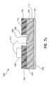
- FIGS. 7 a - 7 b are cut-away-side views showing embodiments of a head region of the flexible printed circuit board, according to embodiments of the invention.
- FIG. 8 is side-view showing an alternative embodiment of a first ferrule and the head region of the flexible printed circuit board, according to an embodiment of the invention.
- FIG. 9 is an exploded view of an embodiment of the housing, an embodiment of the first ferrule, an embodiment of a circuit board mounting structure and an embodiment of the flexible printed circuit board, according to an embodiment of the invention.
- FIG. 10 is a three-dimensional view of an embodiment of the housing, according to an embodiment of the invention.
- FIGS. 11 a - 11 b are diagrams of an embodiment of an apparatus for holding an optical element, according to an embodiment of the invention.
- FIGS. 12 a - 12 d show views of images of optoelectronic devices and images of optical fibers under the high magnification of a split-field microscope.
- FIG. 13 shows the display on a monitor of a video image measuring system.
- a first ferrule 112 packaging an array of optical fibers 114 , is mounted on top of the array of optoelectronic devices 106 in such a manner that one or more of the optical fibers in the array is optically aligned to one or more of the optoelectronic devices.
- a dam 120 may be formed on the flexible printed circuit board 102 and filled with a second adhesive 122 .
- An housing 124 is attached to the circuit board mounting structure 104 , surrounding and enclosing the first ferrule 112 that is connected to the flexible printed circuit board 102 .
- an optical transmitter or receiver module 100 is mounted on a second circuit board 202 , as depicted in FIG. 2 .
- the optical module does not have to be mounted at the board's edge.
- the optical module may be mounted anywhere on the circuit board so long as there is room for connecting the optical module to the external environment.
- the optical module 100 is connected to the external environment by connecting a fiber optic cable 204 to the optical module 100 . This is accomplished by plugging a second ferrule 206 that is attached to one end of a fiber optic cable 204 into the optical module 100 . Once the second ferrule 206 is plugged into the optical module 100 , the module 100 is optically connected to the fiber optic cable 204 .
- the optical module 100 receives electrical signals from the second circuit board 202 , converts the electrical signals into optical signals, and transmits the optical signals into the fiber optic cable 204 .
- the optical module 100 receives optical signals from the fiber optic cable 204 , converts the optical signals into electrical signals and transmits the electrical signals to the second circuit board 202 .
- FIG. 3 a is a cut-away-side view of an embodiment of the flexible printed circuit board 102 .
- the flexible printed circuit board may be bent or folded in any direction, and another embodiment of the flexible printed circuit board is shown in FIG. 3 b .
- the flexible printed circuit board 102 is thin, rectangular and flexible with various edge contours, and it is composed of flexible metal layers that are sandwiched between insulating layers. The entire flexible printed circuit board may be composed of this multi-layered structure.
- the flexible printed circuit board 102 In addition to supporting the electrical components and circuitry of the optical module 100 , the flexible printed circuit board 102 also provides stress relief when connecting the optical module 100 to an external source and aids in maintaining the precise alignment of the optoelectronic devices 106 with an the optical fibers 114 .
- the flexible printed circuit board 102 is bent in the “Y” direction to form a head region 302 , a buckle region 304 and a main body region 306 .
- the head region 302 may function to support the key electrical components and other elements of the optical module 100 , such as the optoelectronic devices 106 and driver or amplifier chip 108 .
- the main body region houses a plurality of electronic components 308 and a plurality of electronic circuitry of the optical module 100 .
- the buckle region 304 is that area of the flexible printed circuit board 102 that connects the head region 302 to the main body region 306 .
- the head region 302 of the flexible printed circuit board 102 is now described in detail, and it is shown in FIG. 3 a or FIG. 3 b .
- the head region 302 is composed of the same multi-layered structure as the other regions of the flexible printed circuit board 102 .
- the head region 302 is orientated in the “Y” direction, and the head region 302 may be on a plane that is substantially perpendicular to the main body region 306 of the flexible printed circuit board 102 , as shown in FIG. 3 a or FIG. 3 b.
- the flexible printed circuit board performs the function of changing the plane on which the signals are received. Specifically, the signals are received by the flexible printed circuit board in the “X” direction from the first ferrule 112 that is optically connected to the optoelectronic devices 106 , which are adapted to the head region 302 of the flexible printed circuit board 102 . The signals then flow in substantially the “Y” direction in the head region 302 of the flexible printed circuit board 102 . The signals then change planes, as they pass from the head region 302 through the buckle region 304 and to the main body region 306 of the flexible printed circuit board 102 , as shown in FIG. 3 a or FIG. 3 b . The signals flow in the “X” direction in the main body region.
- the flexible printed circuit board functions to efficiently communicate with both the fiber optical cable attached to the optical module and an external circuit board upon which the optical module is mounted.
- One board-level component of the head region 302 may be the array of optoelectronic devices 106 .
- the array of optoelectronic devices 106 may be adapted approximately in the center of a first surface 310 and/or the second surface 704 of the head region 302 , as shown in FIG. 3 a or FIG. 3 b .
- the array of optoelectronic devices 106 may be a one-dimensional, two-dimensional or a multi-dimensional array of optoelectronic devices 106 .
- the array of optoelectronic devices 106 may be various types of devices such as edge-emitting lasers, light-emitting diodes (“LEDs”), vertical cavity surface emitting lasers (VCSELs), other surface emitting devices or photo-detectors.
- the optoelectronic devices 106 may also be integrated devices combining one or more devices such as the combination of VCSELs and transistors or photo-detectors and transistors (or VCSELs, photo-detectors and transistors).
- the optoelectronic devices 106 may also be a heterogeneous array where some of the array elements are emitters and some are detectors.
- the optical module 100 functions as a transmitter, sending optical signals into the array of optical fibers 114 that are packaged in the ferrule.
- the optical module 100 functions as a receiver for receiving optical signals from the array of optical fibers 114 packaged in the first ferrule 112 .
- the optoelectronic devices 106 are oxide-confined VCSELs.
- oxide-confined VCSELs operate at higher speeds and have lower threshold currents than non-oxide VCSELs, such as ion-implant VCSELs.
- oxide-confined VCSELs are stable VCSELs, exhibiting uniform power and wavelength performance over varying temperature ranges. This advantageously would allow the module to perform for longer a duration and high degree of accuracy.
- oxide VCSELs would obviate the need for a feedback loop, as hereafter described.
- oxide-confined VCSELs allow the fabrication of highly uniform arrays, enabling multi-channel, parallel optic applications.
- MEMS micro-electromechanical system
- a micro-pipette array or a biological or chemical sample held on a substrate may be used in place of the array of optoelectronic devices 106 .
- Another board-level component of the head region 302 of the flexible printed circuit board 102 may be the driver or amplifier chip 108 , as shown in FIG. 3 a or FIG. 3 b .
- a driver or amplifier chip 108 may be adapted next to the array of optoelectronic devices 106 on the first surface 310 and or the second surface 704 of the head region 302 of the flexible printed circuit board 102 , as shown in FIG. 3 a or FIG. 3 b .
- the driver or amplifier chip 108 may be adapted to the main body region of the flexible printed circuit board.
- the optoelectronic devices 106 are VCSELs
- a driver chip is used, and it functions to drive and modulate the VCSELs.
- the optoelectronic devices 106 are photo-detectors
- an amplifier chip is used, and it amplifies the electronic signals received from photo-detectors.
- Wire bonds 312 or any other suitable means such as plating, welding, tape-automated bonding or the use of flip-chip technology may be used to connect the driver or amplifier chip 108 to the optoelectronic devices 106 , as shown in FIG. 3 a or FIG. 3 b .
- the driver or amplifier chip 108 may be monolithically formed on a semiconductor chip or integrated with the array of optoelectronic devices 106 as a hybrid circuit.
- Still another board-level component of the head region 302 of the flexible printed circuit board 102 may be an optical power control system.
- the optical power control system functions to stabilize the performance of the array of VCSELs over changing conditions.
- the array of optoelectronic devices 106 are transmitters such as VCSELs
- an optical power control system is adapted proximate to the array of optoelectronic devices 106 on the first surface 310 of the head region 302 of the flexible printed circuit board 102 .
- FIG. 4 is an embodiment of the optical power control system.
- the optical power control system utilizes the photo-detector 110 (or alternatively a light-pipe) to measure the optical output power of a VCSEL in an array of VCSELs.
- the optical power control system measures the power of a thirteenth VCSEL 404 in the array of VCSELs.
- the optical power may be measured by any other suitable VCSEL in the array of VCSELs.
- the photo-detector's measurement is used to adjust the electrical power input to each individual VCSEL. This is accomplished by a feedback loop between the photo-detector 110 and the driver chip 108 .
- the driver chip 108 adjusts the laser injection current in response to the feedback, and this results in a stable array of optoelectronic devices.
- FIGS. 5 a - 5 d are diagrams of different optical beam patterns on apertures of photo-detectors.
- the tracking ratio is the ability of the photo-detector 110 to track and capture the optical beam 408 so that the photo-detector 110 accurately measures the amount of power emitted by the VCSEL array.
- the optical beam 408 is fully captured by the photodetector's aperture 502 as shown in FIG. 5 a .
- This allows the photo-detector 110 to precisely measure the power of the beam.
- temperature changes, aging, and other factors during operation can cause the optical beam 408 to become misaligned, as shown in FIG. 5 b .
- the photo-detector's aperture 502 captures less of the optical beam 408 , the photo-detector is unable to accurately measure the beam's power. This causes the optical power control system to improperly adjust the power of the VCSEL array. Similarly as shown in FIG. 5 c , changes in laser injection current and other factors can create a diverged or enlarged optical beam 504 . Again, the photo-detector's aperture 502 detects less power, causing inaccurate adjustments to the power output of the VCSEL array.
- the present invention improves the tracking ratio under changing conditions.
- the present invention accomplishes this task by adapting a reflector/scatterer 410 to a second end of the first ferrule 320 , as shown in FIG. 4 .
- An optical path may be created from the thirteenth VCSEL 404 to the reflector/scatterer 410 and onto the photo-detector 110 .
- the geometry and surface roughness of the reflector/scatterer 410 produces a beam pattern 506 that is highly uniform, scattered and larger than the photo-detector's aperture, as shown in FIG. 5 d .
- This uniform and scattered beam pattern 506 has a high tolerance for alignment and divergence changes. Accordingly, it is less sensitive to temperature changes, aging and other issues.
- this allows the photo-detector 110 to accurately measure the power of the optical beam 408 under varying conditions and environmental circumstances. For example, temperature changes across the VCSEL array may change the optical beam's pattern, alignment and divergence, and this impacts the photo-detector's 110 ability to accurately measure power.
- the highly scattered and uniform beam pattern produced by the reflector/scatterer 410 is significantly less sensitive to temperature changes. This allows the photo-detector 110 to capture the optical beam 504 and accurately measure power.
- the novel beam pattern produced by the unique reflector/scatterer 410 allows the optical power control system to maintain constant power across the VCSEL array under changing conditions. Consequently, the optical power control system produces a stable and uniform VCSEL array.
- the reflector/scatterer 410 is a conical hole that is coated with a reflecting/scattering coating.
- the reflective/scattering coating may be gold, titanium, aluminum or other types materials that have the effect of both reflecting and scattering light.
- the reflector/scatterer 410 may also be an arbitrarily shaped rough surface, sphere, notch, prism or optical element.
- FIG. 6 a An alternative embodiment of the optical power control system is show in FIG. 6 a .
- a glob top of optical resin 602 is coated with a reflective scatterer and is dispensed on the top surface of the array of optoelectronic devices 106 and a top surface of the photo detector 606 .
- the glob top 602 scatters light in multiple directions, and a portion of the light is detected by the photo-detector 110 .
- the shape and coating of the glob top 602 may be engineered to provide varying amounts of scattering for more uniformity and reflection and thus higher energy transfer. As shown by dashed lines in FIG. 6 a , a notch may be cut in the first ferrule 112 to allow room for the glob top of optical resign.
- FIG. 6 b Another embodiment of the optical power control system is show in FIG. 6 b .
- a reflector 608 is formed separately and then adapted to the top surface of the array of optoelectronic devices 106 and to the top surface of the photo detector 606 . Similar to the glob top 602 , the reflector 608 scatters light in multiple directions, and a portion of the light is detected by the photo-detector 110 .
- the shape and coating of the reflector 608 may be engineered to provide varying amounts of scattering for more uniformity and reflecting and thus higher energy transfer.
- the reflector may be in the shape of an ellipsoid, three-dimensional conical hole or other shape. It also may be a geometrically-shaped object.
- the reflector is adapted to the second end 320 of the first ferrule 112 rather than adapted to the top surface of array of optoelectronic devices 106 and photo detector 606 . As shown by dashed lines in FIG. 6 a , a notch may be cut in the ferrule to allow room for the glob top of optical resign.
- An additional board-level component of the head region 302 of the flexible printed circuit board 102 may be a spacer 314 , as shown in FIG. 3 a or FIG. 3 b .
- the spacer 314 may be shaped like a square and may be composed of silicon material.
- a bottom surface of the spacer 314 may be adapted approximately in the center of the head region 302 , as shown in FIG. 3 a or FIG. 3 b .
- a top surface of the spacer 314 may serve as a mounting surface for the array of optoelectronic devices 106 when they function as receivers (e.g., photo-detectors).
- the spacer 314 is optional if the optoelectronic devices 106 function as emitters (e.g., VCSELs).
- the spacer also may function as a mounting surface for other components such as the first ferrule 112 .
- the spacer 314 also may function to raise the height of the array of optoelectronic devices 106 so that a top surface of the array of optoelectronic devices 106 is approximately on the same plane as the other components, such as the driver or amplifier chip 108 , that are adapted on the head region 302 , as shown in FIG. 3 a or FIG. 3 b .
- the wire bonds 312 between the components on the head region 302 more robust and efficient.
- the spacer 314 may be optional if the optoelectronic devices 102 have sufficient height so as to place the second end of the first ferrule 320 at an optimal position above the top surface of the driver or amplifier chip 108 . According to a preferred embodiment, a small interstitial space or gap is maintained between the second end of the first ferrule 320 and the top surface of the optoelectronic devices 102 . In alternative embodiments, this interstitial gap may be omitted.
- the spacer 314 also may function to create or form a gap between the array of optoelectronic devices 106 and the array of optical fibers.
- the spacer 314 may be adjacent to the array of optoelectronic devices.
- the top surface of the spacer 314 may be higher than the top surface of the array of optoelectornic devices 106 .
- the top surface of the spacer may be in contact with the second end of the first ferrule 320 . Accordingly, this creates or forms a gap between the optoelectronic devices and array of optical fibers packaged in the first ferrule.
- the electrical components on the flexible printed circuit board 102 generate heat, and an optoelectronic mounting structure 702 may be used to transmit this heat to the circuit board mounting structure 104 , as explained below.
- FIG. 7 a is a cut-away-side view showing an alternative embodiment of the head region 302 of the flexible printed circuit board 102 , according to an embodiment of the invention.
- the optoelectronic mounting structure 702 has a first surface 710 and a second surface 712 .
- the first surface 710 of the optoelectronic mounting structure 702 passes along a second surface 704 of the head region 302 of the flexible printed circuit board 102 .
- the second surface 712 of the optoelectronic mounting structure 702 is adapted to an upper surface 708 of the circuit board mounting structure 104 with a compliant adhesive.
- the optoelectronic mounting structure may be copper or a similar conductive material.
- the optoelectronic mounting structure may be coated with gold or other adhesion promotion layers such as nickel.
- An window 706 may be formed in the head region 302 of the flexible printed circuit board 102 so as to provide access to the optoelectronic mounting structure 702 .
- the array of optoelectronic devices 106 may be mounted in the window 706 directly on top of the optoelectronic mounting structure 702 . Accordingly, the optoelectronic mounting structure provides a thermal and an electrical contact area for the optoelectronic devices.
- Other electrical components, such as the driver or amplifier chip 108 also may be mounted in the window 706 directly on the optoelectronic mounting structure 702 .
- the optoelectronc mounting structure advantageously 702 dissipates heat generated by the array of optoelectronic devices 106 and other electrical components by spreading the heat and efficiently transmitting it to the circuit board mounting structure 104 .
- the optoelectronic mounting structure 702 also provides an electrical contact path to the optoelectronic devices 106 since the back side of the optoelectronic devices 106 may be gold or copper plated and may be mounted directly to a copper optoelectronic mounting structure 702 .
- the optoelectronic mounting structure 702 may be a solid copper plane, it may acts to limit electromagnetic interference.
- the optoelectronic mounting structure 702 provides electrical shielding by containing any electrical fields that may exist so that the electrical fields do not radiate and create cross talk.
- the optoelectronic mounting structure 702 additionally may provide a stable mounting surface for the optoelectronic devices 106 , and it may function to raise or change the height of the electrical components.
- the optoelectronic mounting structure 702 also provides mechanical rigidity to the head region 302 of the flexible printed circuit board 102 . This mechanical rigidity stiffens the head region 302 and advantageously aids in the assembly process.
- FIG. 7 b is a cut-away-side view showing an alternative embodiment of the head region 302 of the flexible printed circuit board 102 , according to an embodiment of the invention.
- openings 714 in the head region 302 of the flexible printed circuit 102 board may function to dissipate heat to the optoelectronic mounting structure 702 .
- the openings 714 may be heat pipes, thermal vias or similar structures that transmit heat.
- the openings 714 may be formed in the head region 302 so as to provide access to the optoelectronic mounting structure 702 .
- Electrical components, such as the array of optoelectronic devices 106 and the driver or amplifier chip 108 may be mounted on the first surface of the head region 302 . Heat generated by these electrical components may pass through the openings 714 and to the optoelectronic mounting structure 702 .
- the optoelectronic mounting structure 702 dissipates or spreads this heat to the circuit board mounting structure 104 .
- the optical module 100 may include the first ferrule 112 , as shown in FIG. 3 a or FIG. 3 b .
- the first ferrule is mounted on the head region 302 of the flexible printed circuit board 102 . More specifically, the second end of the first ferrule 320 is mounted on the top surface of the array of optoelectronic devices 106 .
- the first ferrule 112 is precisely aligned and attached directly above the active region of the array of optoelectronic devices 106 so that a high coupling efficiency (low loss of light) is achieved.
- each optical fiber 114 in the first ferrule 112 is accurately aligned to a corresponding individual optoelectronic device 106 so that the array of optical fibers 114 inside the first ferrule 112 is optically aligned with the array of optoelectronic devices 106 .
- the precise alignment and attachment of the first ferrule 112 to the array of optoelectronic devices 106 is accomplished by using highly precise machinery and adhesive, and this novel process is explained below.
- the first ferrule 112 may comprise a rectangular ferrule.
- the first ferrule 112 packages an array of optical fibers 114 , extending from a first end 318 of the first ferrule 112 to a second end 320 of the first ferrule 112 .
- Two alignment pins 316 may be adapted to the first end 318 of the first ferrule 112 .
- the alignment pins function to mate the first ferrule 112 to a second ferrule 206 .
- two alignment pin holes may be adapted to the first end 318 of the first ferrule 112 in place of the two alignment pins 318 .
- the alignment pin holes function to mate the first ferrule 112 to a second ferrule 206 .
- FIG. 8 is a side-view showing an alternative embodiment of the first ferrule 112 and the head region 302 of the flexible printed circuit board 102 , according to an embodiment of the invention. Costs are reduced by using a smaller optoelectronic device 106 , as shown in FIG. 8.
- a notch 802 exists at the second end of the first ferrule 320 so that there is sufficient room for wire bonding between the optoelectronic devices 106 and driver or amplifier chip 108 .
- the notch 802 allows positioning the driver chip or amplifier chip 108 in close proximity to the smaller optoelectronic devices 106 . Therefore, the notch 802 obviates the need for long wire bonds to connect the optoelectronic devices to the driver or amplifier chip.
- an array of optical elements may be used in place of the array of optical fibers 114 .
- the optical element may comprise a lenslet array, diffractive optic array, a lens, filter, pipette, capillary tube or optical fibers.
- the optical element does not have to be optical as, for example, in embodiments of the present invention in which biological or chemical analysis is performed.
- the optical element array may be a one-dimensional, two-dimensional or multi-dimensional array of optical elements.
- an array of optical elements or fibers introduces engineering, design, assembly and packaging complexity. This complexity was taken into account in embodiments of the invention. For example, an array of optical elements generates more heat and electromagnetic interference that a single optical element, and this must be considered in all aspects of making and using the device. Also, unlike aligning a single optical element to an optoelectronic device, aligning an array of optical elements to an array of optoelectronic devices is considerably more difficult and complex. Moreover, an array of optical elements can more readily become effected by electrical or optical cross-talk since the optical elements are closely coupled. Therefore, the array is highly subject to signal degradation, and design limitations must be made to take these factors into account.
- a first adhesive 116 is dispensed on the top surface of the array of optoelectronic devices 106 , as shown in FIG. 3 a or FIG. 3 b .
- the first adhesive is preferably an optically clear adhesive or a gel that has a complementary index of refraction to the optical fibers 114 .
- the first ferrule 112 is held suspended above the top surface of the array of optoelectronic devices 106 in the first adhesive 116 .
- the optical adhesive 116 may be cured with UV light, RF radiation, air, microwave radiation or thermal means, depending on the type of adhesive that is used. Once the optical adhesive 116 is cured, the space or gap between the second end of the first ferrule 320 and the top surface of the optoelectronic devices 118 is preserved or set; this space having been filled with the first adhesive 116 . In other words, a thin layer of first adhesive 116 exists at the interface between the second end of the first ferrule 320 and the top surface of the optoelectronic devices 118 .
- the first adhesive 116 functions to stabilize and hold the first ferrule 112 to the array of optoelectronic devices 106 .
- the first adhesive 116 maintains the precise alignment of the array of optical fibers 114 packaged in the first ferrule 112 to the array of optoelectronic devices 106 .
- the first adhesive also functions to maintain the gap that exists between the first ferrule 112 and array of optoelectronic devices 106 .
- the first adhesive 116 produces a high coupling efficiency between the array of optical fibers 114 packaged in the first ferrule 112 and the array of optoelectronic devices 106 .
- the first adhesive 116 is an optically clear adhesive or gel and has almost the same refractive index as the optical fibers. Accordingly, by providing a refractive index match to the optical fibers, light passing from the array of optoelectronic devices 106 to the array of first fibers 114 (or vice versa) experiences minimal Fresnel reflection loss and optical divergence over the gap distance that exists between the array of optoelectronic devices 106 and the array of first fibers 114 .
- the first adhesive 116 also serves to prevent air from existing at the interface or space between the first ferrule 112 and the array of optoelectronic devices 106 .
- the elimination of air at the interface or gap is desirable because air has a lower refractive index than the optoelectronic devices 106 , the optical fibers 114 and the first adhesive 116 .
- the refractive index difference introduces reflection losses, and the lower reflective index results in greater beam divergence per unit propagation length.
- the first adhesive prevents a second adhesive 122 from inadvertently seeping or wicking into the gap or space between the bottom surface of the ferrule and the top surface of the optoelectronic devices. Consequently, the first adhesive 116 advantageously produces a high-coupling efficiency between the optoelectronic devices 106 and the optical fibers 114 that are packaged in the first ferrule 112 .
- the first adhesive 116 not only enhances the coupling efficiency between the optical fibers 114 and optoelectronic devices 106 by providing a refractive index match to the optical radiation, but it also serves another important purpose. Specifically, the first adhesive 116 provides mechanical robustness by securing the first ferrule 112 to the array of optoelectronic devices 106 . As previously stated, the gap or space between the bottom surface of the first ferrule 112 and the top surface of the optoelectronic devices 118 is filled with the first adhesive. The first adhesive functions to mechanically stabilize the first ferrule 112 to the head region 302 of the flexible printed circuit board 102 .
- the first adhesive 116 provides support for any lateral, axial or rotational strain that may be created when a fiber optic cable is attached to the optical module. Furthermore, this allows proceeding to the dam and well-fill step, which is explained below, with minimal or no supporting structure to maintain the precision axial alignment of the array of optical fibers 114 packaged in the first ferrule 112 to the array of optoelectronic devices 106 . Accordingly, the first adhesive 116 advantageously reduces manufacturing time and costs by providing mechanical robustness in addition to providing high coupling efficiency.
- the first adhesive mechanically stabilizes the first ferrule 112 to the head region 302 of the flexible printed circuit board 102 .
- a second adhesive 122 may be adapted to the head region 302 to further mechanically stabilizes the first ferrule 112 to the head region 302 of the flexible printed circuit board 102 , as shown in FIG. 3 a or FIG. 3 b .
- the second adhesive 122 may provide support for any lateral, axial or rotational strain that may be created when a fiber optic cable is attached to the optical module. No dam is necessary to form the first adhesive 116 .
- a dam 120 may be formed on the head region 302 and filled with the second adhesive 122 , as shown in FIG. 3 a or FIG. 3 b .
- the second adhesive may be used without the dam.
- the dam may be constructed or dispensed, and the dam 120 may be dispensed and formed in a single or multi-layered path.
- the dam 120 may be in the shape of a square, diamond, oval or any other shape that effectively stabilizes and encloses the optoelectronic devices and possibly wire bonds and other die on the head region 302 of the flexible printed circuit board 102 .
- the dam 120 may furthermore surround and enclose all of the components on the head region 302 for extra protection.
- the dam 120 may be constructed and formed on the first surface 310 of the head region 302 of the flexible printed circuit board 102 .
- the dam 120 may surround the first ferrule 112 , driver or amplifier chip 108 or other electrical components, as shown in FIG. 3 a or FIG. 3 b .
- the dam 120 may be composed of adhesive or epoxy.
- the dam 120 may be formed or built by dispensing several layers of adhesive or epoxy on top of each other over time until the desired height and width of the dam 120 is achieved.
- the adhesive or epoxy may be any standard well-fill or potting epoxy. Alternatively, as previously stated, the dam may be dispensed and formed in a single path.
- the area within the dam may be filled with the second adhesive 122 .
- the second adhesive 122 preferably covers the driver or amplifier chip 108 , array of optoelectronic devices 106 , and any other electrical components that are adapted to the head region 302 , as shown in FIG. 3 a or FIG. 3 b .
- a sufficient amount of second adhesive 122 is poured inside the dam area so that the height of the second adhesive 122 may span from the first surface 310 of the head region 302 of the flexible printed circuit board 102 to somewhere below the first end 318 of the first ferrule 112 , as shown in FIG. 3 a or FIG. 3 b .
- the dam 120 and second adhesive 122 function to mechanically stabilize the first ferrule 112 to the first surface 310 of the head region 302 of the flexible printed circuit board 102 .
- the dam 120 and second adhesive 122 may provide additional mechanical support to further stabilize the first ferrule 112 to the head region 302 of the flexible printed circuit board 102 .
- the dam 120 and second adhesive 122 may function to absorb stress and provide rigidity and strength that may be needed when connecting the optical module to an external environment such as a fiber optic cable. Also, the dam 120 and second adhesive 122 may prevent movement that may occur over temperature variances. Moreover, the dam 120 and second adhesive 122 may function to provide moisture blocking and protection to the electrical components and circuitry adapted to the first surface 310 of the head region 302 of the flexible printed circuit board 102 .
- the surface area of the second adhesive 122 may be covered with a third layer.
- the third layer may protect the optical module by blocking the permeation of moisture and providing electric shielding.
- the third layer may be a conductive and or moisture blocking adhesive such as gel silicon resin. It may also be a metallic, dielectric or other type of coating that provides necessary protection to the optical module.
- an attenuator may be used that functions to modify the performance of the array of optoelectronic devices. Specifically, superior performance of the array of optoelectronic devices typically is found if such devices are operated at the midpoint rather than low-point of their power range. However, operating the optoelectronic devices at the mid-point of their power range may not meet optical output requirements.
- One solution is to operate the optoelectronic devices at the mid-point of their power range but not transmit all of the power out of the end of the array of optical fibers. This may be accomplished through the use of the attenuator.
- the attenuator may function to reflect, absorb and or scatter the optical output of at least one optoelectronic device. Also, the attenuator advantageously may control optical cross-talk, reduce back-reflection and may eliminate feedback noise.
- the attenuator may be a coating on the first or second end of the first ferrule or a coating on the first or second end of the array of optical elements that are packaged in the ferrule. It also may comprise a coating on the first end of the array of optoelectronic devices.
- the coating may be a metal, dialetric, organic or other material, and the coating may be patterned.
- Another embodiment of the attenuator may be a gel-like substance that is deposited in the gap that exists between the first end of the optoelectronic devices and the first end of the optical fibers. In this embodiment, the attenuator would function to absorb some of the light emitted by the optoelectronic devices.
- Attenuator may be increasing the absorption of the first adhesive, introducing a controlled seeping or wicking of an absorbing second adhesive, changing the gap distance to reduce coupling, changing the refractive index to introduce Fresnel reflection and introduce divergence, changing the lateral alignment, or changing the surface finish of the optical fibers.
- other embodiments of the attenuator may include changing the optical transmission characteristics of the array of optical fibers so that they absorb, reflect and or scatter light. In this manner, the optical energy exiting the array of optical fibers will have its signal power reduced. This may be accomplished by changing the surface finish of the cores of the optical fibers (e.g., using frosted, wavy or rough surface glass) or by coating the inner surfaces of the fiber optic cores.
- a conditioner may be used to improve the performance of the array of optical fibers by changing the way the optical energy is launched into the optical fibers. For example, conditioning the launch of optical energy can improve the effective bandwidth of the optical fibers.
- the conditioner may function to change the phase distribution of the optical energy that is emitted by the optoelectronic devices.
- Conditioning the launch of the optical energy flowing into the optical fibers from the optoelectronic devices may be accomplished as follows: (1) patterning a coating on the first end of the array of optoelectronic devices; (2) patterning a coating on the first or second end of the array of optical fibers; (3) depositing a gel-like substance between the first end of the optoelectronic devices and the first end of the optical fibers; (4) adapting a diffractive object on the input or output of the array of optical fibers so as to change the structure of the optical energy; (5) changing the lateral position of the array of optoelectronic devices relative to the array of optical fibers; (6) changing the optical transmission characteristics of the array of optical fibers; (7) tilting the array of optoelectronic devices relative to an optical path; and (8) changing the optical transmission characteristics of the array of optical fibers so that they absorb, reflect and or scatter light.
- the flexible printed circuit board 102 also comprises a buckle region 304 , which will now be described with reference to FIG. 3 a or FIG. 3 b .
- the buckle region 304 is that area of the flexible printed circuit board 102 connecting the head region 302 to the main body region 306 of the flexible printed circuit board 102 .
- the buckle region 304 is thin and composed of the same multi-layered structure as the other regions of the flexible printed circuit board 102 .
- a plurality of electrical circuitry may be adapted both to a first surface and a second surface of the buckle region 304 .
- the electrical circuitry functions to electrically connect the head region 302 to the main body region 306 of the flexible printed circuit board 102 .
- the buckle region functions to absorb any stress and misalignment that may occur when the head region 302 and main body region 306 are connected to the circuit board mounting structure 104 during the assembly process. Specifically, after the head region 302 is attached to the circuit board mounting structure 104 , the flexible printed circuit board 102 is wrapped or folded around and attached to the circuit board mounting structure 104 , as explained in detail below. Alternatively, the main body region 306 may be first connected to the circuit board mounting structure 104 followed by folding the flexible printed circuit board and connecting its head region 302 to the circuit board mounting structure 104 . The housing 124 is then connected to the circuit board mounting structure 102 .
- the first ferrule 112 which is adapted to and protrudes from the head region, is then aligned and housed in a longitudinal cavity 1006 of the housing 124 .
- stress or misalignment may occur when connecting the housing 124 to the circuit board mounting structure 104 .
- the buckle region 304 functions to absorb any misalignment or stress that may occur during this assembly process. As shown in FIG. 3 a or FIG. 3 b , the buckle region 304 bends in the “Y” direction. Bending the buckle region 304 provides the buckle region 304 with bending freedom in the x, y and z direction, as well as rotational freedom. This bending freedom allows the buckle region 304 to absorb any stress that may occur during the assembly process when aligning and attaching the housing 124 to the circuit board mounting structure 104 .
- the flexible printed circuit board 102 also comprises a main body region 306 .
- the main body region 306 will now be described with reference to FIG. 3 a or FIG. 3 b .
- the main body region 306 is thin, rectangular shaped and flexible.
- the main body region 306 is composed of the same multi-layered structure as the other regions of the flexible printed circuit board.
- the main body region 306 functions to house the other electrical components and circuitry of the optical module 100 .
- the electrical components may serve a variety of functions, including connection of the optical module to the system to which it is located.
- a plurality of electrical components 308 and a plurality of electrical circuitry may be adapted to a first surface 324 and/or a second surface 326 of the main body region 306 of the flexible printed circuit board 102 , as shown in FIG. 3 a or FIG. 3 b.
- a series of electrical connections may be adapted to the first or second surface 324 of the main body region 324 of the flexible printed circuit board 102 .
- the electrical connections function to electrically connect the flexible printed circuit board to an external environment such as another circuit board.
- the electrical connections may comprise ball grid arrays, solder balls, wire leads, land-grid arrays with conductive interposers, or any other means to electrically connect the flexible printed circuit board to an external environment.
- the flexible printed circuit board 102 supports the main electrical components and elements of the optical module, such as the optoelectronic devices 106 , driver or amplifier chip 108 and first ferrule 112 , as well as providing bending freedom and stress relief to the optical module 100 .
- the flexible printed circuit board 102 is attached to, and partially enclosed by, a housing 902 , which is described below.
- FIG. 9 is an exploded view of the flexible printed circuit board 102 , first ferrule 112 , a circuit board mounting structure 104 and an housing 124 .
- the circuit board mounting structure 104 functions in part as a mounting structure for the flexible printed circuit board and as a heat sink to dissipate heat generated by the circuit board 102 .
- the flexible printed circuit board 102 is bent and wrapped around the circuit board mounting structure 104 .
- a second surface 904 of the flexible printed circuit board 102 is attached to a bottom surface 914 and a first end 910 of the circuit board mounting structure 104 , as shown in FIG. 9 .
- Alignment ridges, guide pins or guide pin holes may exist along the bottom surface 914 and first end 910 of the circuit board mounting structure, although they are not necessary.
- the alignment features assist in aligning and holding the flexible printed circuit 102 board to the circuit board mounting structure.
- a fourth adhesive is used to firmly attach the flexible printed circuit board 102 to the circuit board mounting structure 104 .
- the thermal expansion coefficient and compliance of the fourth adhesive advantageously assists in preventing expansion or contraction of the circuit board mounting structure from damaging the flexible printed circuit board 102 .
- the flexible printed circuit board 102 bends around the circuit board mounting structure 104 in such a manner that the head region 302 of the flexible printed circuit board 102 is housed inside the first end 910 of the circuit board mounting structure 104 , as shown in FIG. 9.
- a cavity 912 on the first end 910 of the circuit board mounting structure 104 functions to house the head region 302 of the flexible printed circuit board 102 . In another embodiment, there is no cavity 912 , as explained below.
- a series of heat sink ridges adapted to the circuit board mounting structure function to dissipate heat generated by the flexible printed circuit board.
- the second surface 704 of the head region 302 of the flexible printed circuit board 102 is attached to the first surface 710 of the optoelectronic mounting structure 702 .
- the second surface 712 of the optoelectronic mounting structure 702 is attached to the upper surface 708 of the circuit board mounting structure 104 with a compliant adhesive.
- the flexible printed circuit board 102 then wraps around the circuit board mounting structure 104 so that the remaining portion of the second surface 904 of the flexible printed circuit board is attached to the bottom surface 914 of the circuit board mounting structure 104 , as shown in FIG. 9 .
- the circuit board mounting structure has feet 916 for connecting the optical module 100 to an external environment such as a second circuit board 202 .
- the feet 916 have ridges that allow a portion of each foot 916 to drop into a hole on the second circuit board 202 and therefore attach and align the optical module 100 to the second circuit board 202 .
- the ridges on the feet also maintain the optical module 100 at a specified distance above the second circuit board 202 .
- the circuit board mounting structure 104 has snap slots 906 , set screw holes and or alignment pin holes on the first end 910 for connecting the first end of the circuit board mounting structure to housing 124 , as discussed in detail below.
- the housing 124 is connected to the circuit board mounting structure 104 , and the housing 124 will now be described in detail with reference to FIG. 10 .
- the housing 124 may be made of a non-conductive material.
- the housing 124 comprises a mating end 1002 , as shown in FIG. 10 a , and a receiving end 1004 , as shown in FIG. 10 b.
- a longitudinal cavity 1006 extends through the housing 124 from the mating end 1002 to the receiving end 1004 , as shown in FIGS. 10 a - 10 b.
- the mating end 1002 of the housing 124 has tabs 1008 and alignment pins 1010 for connecting the mating end 1002 to the first end 910 of the circuit board mounting structure 104 , as shown in FIG. 10 a .
- the position of the tabs 1008 correspond to the position of the snap slots 906 located on the first end 910 of the circuit board mounting structure 104 .
- the position of the alignment pins 1010 correspond to the position of the alignment pin holes on the first end 910 of the circuit board mounting structure 104 . (See FIG.
- the housing 124 snaps on to the circuit board mounting structure 104 and is firmly attached.
- the housing is snapped onto the circuit board mounting structure.
- the housing may be connected by using other attachment methods such as glue, screws or through the use of other mechanical fixtures.
- inserts may be adapted to the mating end of the housing that function to hold the circuit board mounting structure to the housing. The inserts aid in applying a force to the tabs that maintain the tabs firmly in place. These inserts may be in the form of wedges, spring-clips, stakes or shims.
- alignment members on the mating and receiving ends of the housing function to hold and align the position of the first and second ferrules relative to the position of the housing.
- These alignment members may be inwardly sloping walls at an opening of the longitudinal cavity.
- the alignment members act independently or in concert with the alignment pins and tabs to align and connect the first ferrule and the circuit board mounting structure.
- At least one elastomeric pressure ring 1012 that is in proximity to the housing 124 functions to secure the housing 124 and the head region 302 of the flexible printed circuit board 102 to the circuit board mounting structure 104 .
- the elastomeric pressure ring 1012 may be in a variety of shapes and forms such as a circular, oval spaces or donuts, as shown in FIG. 9 .
- the elastomeric pressure ring 1012 has multiple purposes.
- the elastomeric pressure ring 1012 is compressed, and this compression creates an outward elastomeric force in the direction of the receiving end 1004 of the housing 124 that maintains the tabs 1008 and the snap slots 906 in a firmly locked position. With the compression force on the tabs 1008 and snap slots 906 , a high degree of manufacturing tolerances is achieved. Second, the pressure or force created by the compressed ring 1012 aids in bonding the optoelectronic mounting structure 702 to the circuit board mounting structure 104 .
- the optoelectronic mounting structure 702 is bonded to the circuit board mounting structure 104 with adhesive, and the pressure produced by the compressed ring 1012 holds the optoelectronic mounting structure 702 firmly against the circuit board mounting structure 104 while the adhesive is cured. Accordingly, the elastomeric pressure ring 1012 produces tighter bonding between the circuit board mounting structure 104 and the optoelectronic mounting structure 702 . Third, once the housing 124 is snapped onto the circuit board mounting structure 104 , the pressure or force created by the elastomeric pressure ring 1012 provides a more robust moisture seal between the housing 124 and the circuit board mounting structure 104 .
- the first ferrule 112 Upon attachment of the housing 124 to the circuit board mounting structure 104 , the first ferrule 112 is housed in the longitudinal cavity 1006 of the housing 124 , and alignment ridges inside the longitudinal cavity 1006 engage and hold the first ferrule 112 in place.
- the housing 124 slides into the circuit board mounting structure 104 , and the head region 302 of the flexible printed circuit board 102 is buried in the cavity 912 of the first end 910 of the circuit board mounting structure 104 .
- the first end 910 of the circuit board mounting structure 104 may not have a cavity, and the head region 302 may exist on the outside of the first end 910 of the circuit board mounting structure 104 .
- the housing 124 instead of having the housing 124 slide into the circuit board mounting structure 104 , the housing 124 may slide over the circuit board mounting structure 104 , and the head region 302 may be housed in a cavity inside the housing 124 .
- neither the housing 124 nor the circuit board mounting structure 104 may have a cavity, and the two parts simply may mate with each other.
- a metallic coating may be applied to at least a portion of the mating end 1002 of the housing 124 .
- the metallic coating functions to provide electromagnetic shielding.
- the housing may be made out of multiple materials and at least one of those materials would function to provide electromagnetic shielding.
- the receiving end 1004 of the housing 124 functions to connect the optical module 100 to an external system.
- the receiving end 1004 receives a second ferrule 206 , which is typically attached to one end of a fiber optic cable 204 .
- the second ferrule mates with the first ferrule, as described below.
- the second ferrule 206 may be a MT type connector, MU type connector, MPO type connector or other type connectors.
- the second ferrule 206 is inserted into the receiving end 1004 of the housing 124 .
- Wings 1014 snaps or beams on the receiving end 1004 align, grab and hold the second ferrule 206 , and the wings 1014 snap onto the second ferrule 206 .
- the wings 1014 function to provide alignment compliance when connecting the second ferrule 206 to the housing 124 .
- the wings 1014 are flexible and may absorb any stress that may arise due to movement of the cable 204 that is attached to the second ferrule 206 .
- the wings 1014 further provide a holding force that aids in holding the second ferrule 206 to the first ferrule 112 . Alignment ridges inside the longitudinal cavity 1006 of the housing 124 further engage and hold the second ferrule 206 in place.
- the second ferrule 206 mates with the first ferrule 112 that is also housed in the longitudinal cavity 1006 of the housing 124 .
- the second ferrule 206 mates with the first ferrule 112 by engaging the alignment pins 316 located on the first end 318 of the first ferrule 112 with alignment pin holes located on a mating end of the second ferrule 206 .
- the alignment pins 316 and alignment pin holes function to provide fine alignment between the mating arrays of optical fibers that are packaged within the mating ferrules.
- the first ferrule may have alignment holes and the second ferrule may have alignment pins, and the ferrules would accordingly mate in a similar fashion.
- the array of optical fibers that are packaged in the ferrules are axially aligned, and the ferrules are optically connected.
- the optical module 100 functions as a receiver, optical signals pass from the fiber optic cable 204 , through the optical fibers packaged in the ferrules 206 and 112 and to the optoelectronic devices 106 , which are mounted on the flexible printed circuit board 102 .
- the optical module 100 converts the optical signals into electrical signals and transmits these signals to an external environment, such as a printed circuit board, for processing.
- An important aspect of an embodiment of the invention is the precise alignment and attachment of the first ferrule 112 to the array of optoelectronic devices 106 that are mounted on the flexible printed circuit board 102 .
- a process, according to an embodiment of the invention, for aligning and connecting the first ferrule 112 to the array of optoelectronic devices 106 comprises the following steps:
- a high-precision alignment machine may be used in combination with a series of other apparatuses to produce precise alignment and attachment of optical fibers to optoelectronic devices.
- These machines combine many critical technologies to perform alignment with a low-cost manufacturing environment. These technologies include: (1) a high-precision stage that is used to hold the flexible printed circuit board 102 ; (2) a high-precision alignment arm for accurately placing the first ferrule 112 on the optoelectronic devices 106 that are adapted to the flexible printed circuit board 102 ; (3) a top-down view camera; (4) side-view camera; (5) video monitors; (6) split-field microscope; and (7) optical video system function together to replace the labor-intensive active-alignment process.
- computers and software may perform many of above-stated technologies. An example of one of the many process that may be used with this equipment is explained in the following paragraphs.
- the first step in the precise alignment and attachment of the first ferrule 112 to the array of optoelectronic devices 106 is to hold the first ferrule 112 at the end of a high-precision stage. This is accomplished through the use of an apparatus for holding an optical element, as explained in this section.
- FIGS. 11 a - 11 b show views of an embodiment of the apparatus for holding an optical element.
- the apparatus for holding an optical element 1100 holds the first ferrule 112 through the use of pin-positioning holes 1102 and vacuum pressure.
- the apparatus for holding an optical element has a first end 1112 and a second end 1114 .
- the apparatus for holding an optical element 1100 may have two pin-positioning holes 1102 on a bottom surface 1104 of the second end 1114 for receiving the alignment pins 316 of the first ferrule 112 , as shown in FIGS. 11 a - 11 b . As shown in FIG.
- an array of optical fibers 1106 may be packaged between the pin-positioning holes 1102 , and it is optically aligned with the array of optical fibers 114 that are packaged in the first ferrule 112 .
- the innermost optical fibers in the apparatus for holding an optical element 1100 are milled out, forming a longitudinal cavity 1108 running through the apparatus for holding an optical element 1100 from the first end 1112 to the second end 1114 , as shown FIG. 11 b .
- a vacuum is placed at a top surface of the first end 1112 of the longitudinal cavity 1108 , and the longitudinal cavity 1108 functions as a vacuum slot.
- the vacuum slot functions as a vacuum clamp, holding the first ferrule 112 in place.
- an electrostatic clamp may be used in place of the vacuum clamp.
- another embodiment may comprise alignment pins in place of the pin-positioning holes 1102 , and the alignment pins would function to connect to pin-positioning holes in a ferrule.
- the apparatus for holding an optical element 1100 has multiple advantages and uses. First, it permits holding and manipulating the first ferrule 112 in both the x, y, and z direction as well as rotational directions. This aids in achieving precise alignment and attachment of the first ferrule 112 to the optoelectronic devices 106 . Also, the apparatus for holding an optical element 1100 grasps the first ferrule 112 without interfering, obscuring or damaging the optical fibers 114 in the first ferrule 112 . Additionally, the apparatus for holding an optical element 1100 allows access to the optical fibers 114 in the first ferrule 112 so that optical coupling may be achieved.
- a light may be mounted on top of the apparatus for holding an optical element 1100 so that the optical fibers 114 emit light while being held by the apparatus for holding an optical element 1100 .
- the light emitted from the fibers 114 may then be used to aid in optically coupling the first ferrule 112 to the optoelectronic devices 106 .
- light from the optoelectronic devices may be used to aid in optically coupling the first ferrule 112 to the optoelectronic devices 106 .
- the apparatus for holding an optical element 1100 provides a strain-less release mechanism through the use of the vacuum clamp. By simply turning off the vacuum pressure, the apparatus for holding an optical element 1100 gently releases the first ferrule 112 .
- the apparatus for holding an optical element 1100 also may be used for a variety of different purposes other than holding a ferrule. For example, it may be used to align and attach a micro-pipette array to a biological sensor array or a lens array to a MEMS modulator array. It also may be used to attach a single or array of optical fibers to a variety of different objects or devices.
- the optical element may be a MT type connector, ferrule, MT-like ferrule, lenslet array, a diffractive optical element or any other type of device that may be aligned with the device. Accordingly, the apparatus for holding an optical element 1100 has multiple advantages and uses.
- the next step is to align the optical fibers with the optoelectronic devices in the x, y and rotational directions. In this section, three different alignment process are described.
- the first process for aligning the optical fibers with the optoelectronic devices in the x, y and rotational directions is an image alignment process.
- a split-field microscope is used to align the optical fibers with the optoelectronic devices by super-imposing an image of at least one optical fiber with an image of at least one optoelectronic devices.
- the array of optoelectronic devices, which are mounted on a flexible printed circuit board are held on a high-precision stage.
- a top-down view camera may be mounted above the high-precision stage holding the optoelectronic devices.
- a light is mounted above the high-precision arm, emitting optical radiation down into the optical fibers 114 that are packaged in the first ferrule 112 .
- the light flowing down the optical fibers back-lights the fiber cores, and this provides a well-resolved image of the fiber cores under the split-field microscope.
- the image of the cores then appear as an array of well-resolved spots under the split field microscope, as shown in FIG. 12 c.
- This process precisely aligns in the x, y and rotational direction the array of optical fibers 114 that are packaged in the first ferrule 112 with the array of optoelectronic devices 106 that are adapted to the flexible printed circuit board 102 .
- images of the optical fibers and optoelectronic devices other than the images of the first and twelfth optical fibers and optoelectronic devices may be used to achieve the same result.
- a second process to align the optical fibers with the optoelectronic devices in the x, y and rotational directions is an optical energy alignment process.
- the flexible printed circuit board is again held by a high-precision stage.
- a light is mounted above the high-precision arm that holds the first ferrule, and the light emits optical radiation down into the optical fibers 114 that are packaged in the first ferrule 112 .
- the light flowing out of the optical fibers 114 radiates down onto the flexible printed circuit board 102 , which is positioned on the high-precision alignment stage. Under the high magnification of a microscope, this light appears as a series of illuminating spots on the optoelectronic devices 106 .
- Each illuminating spot corresponds to an optical fiber in the array of optical fibers 114 that are packaged in the first ferrule 112 .
- the spots may be visually aligned with the rings to form a bull's eye pattern under the high magnification of a microscope. (This alignment process may be performed by machine vision rather than by human vision.)
- the alignment process precisely aligns in the x, y and rotational direction the array of optical fibers 114 that are packaged in the first ferrule 112 with the array of optoelectronic devices 106 that are adapted to the flexible printed circuit board 102 .
- a third process to align the optical fibers with the optoelectronic devices in the X, Y and rotational directions is a precision placement system.
- a precision placement system is connected to a high-precision arm that holds the first ferrule, and the system also is connected to a high-precision stage that holds the optoelectronic devices.
- the precision placement system aligns the objects by first calculating their initial position in space by comparing their position to a known position in space. Based upon this information, the system calculates the relative distances that the objects are apart. Once the relative distances are determined, the precision placement system aligns the objects by sequentially moving the objects and re-calculating their relative distances until they are precisely aligned.
- the precision placement system may determine the initial position in space of the array of optical fibers and the optoelectronic devices by holding the objects within a field of view of a microscope. Since the position of the cross-hairs on the microscope is known, the precision placement system knows the position of the optical fibers and optoelectronic devices relative to the position of the cross-hairs. Based upon this information, the precision placement system then calculates the relative positions of the objects to each other. Knowing the relative distances, the precision placement sequentially and continually moves the position of the objects and re-calculates their relative positions to each other until the optical fibers and optoelectronic devices are precisely aligned.
- the high-precision alignment arm is lowered until the first ferrule 112 is within a few microns from the optoelectronic devices 106 .
- This vertical or Z-axis alignment process is accomplished through the use of a video-image measuring system that functions in concert with the previously-described precision equipment. This z-axis alignment process is described below.
- a video-image measuring system is connected between a monitor and a side-view camera that is mounted near the side of the high-precision stage. With the aid of the microscope, the side-view camera views the side of the optoelectronic devices 106 and first ferrule 112 , and this image is displayed on the monitor.
- FIG. 13 is a view of the monitor when using the video-image measuring system.
- the video image measurement system generates positional measuring lines 1302 over the images on the monitor, and the lines 1302 allow a user to measure the vertical distance or Z-axis height between a bottom edge 1304 of the first ferrule 112 and a top edge 1306 of the optoelectronic devices 106 , as shown in FIG. 13 .
- the distance between the bottom edge 1304 of the first ferrule 112 to the top edge 1306 of the optoelectronic devices 106 is adjusted until the objects are within a few microns (e.g., approximately 35 microns apart). Accordingly, a gap exists between the first ferrule 112 and the optoelectronic devices 106 .
- the z-axis alignment process may be accomplished by using laser-triangulation, interference microscophy or a touch sensor.
- the high-precision placement arm is raised, moving the first ferrule 112 away from the optoelectronic devices 106 in the vertical or Z-axis direction.
- a small volume of first adhesive 116 is then dispensed on the top surface of the optoelectronic devices 106 by a high precision, motor-driven syringe.
- the high-precision placement arm is again lowered in the vertical or Z-axis direction until the first ferrule 112 contacts the optical adhesive 116 , which has been dispensed on the top surface of the optoelectronic devices 106 .
- the first ferrule 112 is suspended above the top surface of the optoelectronic devices in the liquid optical adhesive 116 .
- the first adhesive 116 may be cured using a UV light curing system.
- the first ferrule 112 is attached to the optoelectronic devices 106 with the first adhesive 116 and is held from above by the apparatus for holding an optical element 1100 .
- the first adhesive mechanically stabilizes the first ferrule 112 to the optoelectronic devices 106 .
- the first ferrule 112 is separated from the apparatus for holding an optical element 1100 releasing the vacuum clamp on the apparatus for holding an optical element 1100 and raising the high precision alignment arm.
- a dam 120 may be formed on the flexible printed circuit board 102 and filled with the second adhesive 122 .
- a software-controlled dam and dam fill dispensing machine may be used to apply the dam 120 on the first surface 310 of the head region 302 of the flexible printed circuit board 102 .
- the dam and filling process may be done manually.
- the dam 120 is formed on the first surface 310 of the head region 302 of the flexible printed circuit board 102 surrounding the first ferrule 112 , driver or amplifier chip 108 and any other electrical components.
- the dam 120 is composed of an adhesive .
- the automated fluid dispensing machine may be used to fill the area within the dam 120 with the second adhesive 122 , as shown in FIG. 3 a .
- the second adhesive 122 may be cured by placing the flexible printed circuit board 102 in an oven. After curing, the first ferrule 112 becomes further mechanically stabilized to the first surface of the head region 302 of the flexible printed circuit board 102 .
- the entire process of precisely aligning and attaching the first ferrule 112 to the optoelectronic devices 106 and mechanically stabilizing it to the flexible printed circuit board 102 may be done manually. Alternatively, this process may be done automatically through the use of a computer generated system that functions in concert with the above-described precision equipment. Accordingly, this process is compatible with a mass-production manufacturing process that is the type of technology that is necessary to lower the cost of any commercially-available high-volume product.
- an embodiment of the invention has been discussed in terms of accurately aligning and attaching an array of optical fibers to an array of optoelectronic devices, the same methodology may be employed to accurately align and connect an array of optical fibers to a wide variety of devices or objects other than optoelectronic devices. This is because there is a trend to miniaturization in many fields of science and technology that require work pieces to be positioned to a few microns and many times to sub-microns. Such fields include optics, microscopy, semiconductor technology, micro-machining, the life sciences and others. Accordingly, an embodiment of the invention may be used, for example, to accurately align and connect optical fibers to a microscope slide so as to study fluorescence light emitted from a biological sample such as a gene or insect.
- an embodiment of the invention may be used to accurately align and connect an array of optical fibers to micro-electromechanical systems (“MEMS”).
- MEMS technology involves combining semiconductor and micro-machining processes to produce tiny devices that are capable of motion on a microscopic scale on a silicon substrate.
- These systems may utilize the technology contained in an embodiment of the invention to accurately align and connect an array of optical fibers to the tiny devices in the micro-electromechanical system for a wide variety of applications. Consequently, an embodiment of the invention may be used to couple an array of optical fibers to a wide variety of devices or objects.
- an embodiment of the invention has been discussed in terms of passive alignment, an embodiment of the invention allows for active alignment and attachment of the array of optical fibers to an array of optoelectronic devices. As explained earlier, this process involves manually manipulating and connecting the optical fibers to the optoelectronic devices.
Abstract
Description
Claims (82)
Priority Applications (2)
| Application Number | Priority Date | Filing Date | Title |
|---|---|---|---|
| US09/749,283 US6799902B2 (en) | 2000-12-26 | 2000-12-26 | Optoelectronic mounting structure |
| PCT/US2001/043265 WO2002103427A2 (en) | 2000-12-26 | 2001-11-20 | Optoelectronic mounting structure |
Applications Claiming Priority (1)
| Application Number | Priority Date | Filing Date | Title |
|---|---|---|---|
| US09/749,283 US6799902B2 (en) | 2000-12-26 | 2000-12-26 | Optoelectronic mounting structure |
Publications (2)
| Publication Number | Publication Date |
|---|---|
| US20020122636A1 US20020122636A1 (en) | 2002-09-05 |
| US6799902B2 true US6799902B2 (en) | 2004-10-05 |
Family
ID=25013086
Family Applications (1)
| Application Number | Title | Priority Date | Filing Date |
|---|---|---|---|
| US09/749,283 Expired - Lifetime US6799902B2 (en) | 2000-12-26 | 2000-12-26 | Optoelectronic mounting structure |
Country Status (2)
| Country | Link |
|---|---|
| US (1) | US6799902B2 (en) |
| WO (1) | WO2002103427A2 (en) |
Cited By (10)
| Publication number | Priority date | Publication date | Assignee | Title |
|---|---|---|---|---|
| US20040126068A1 (en) * | 2001-03-16 | 2004-07-01 | Van Bijsterveld Cornelis Casparus | Method for providing a broadband infrastructure in a building by means of optical fibres |
| US20070076381A1 (en) * | 2005-08-18 | 2007-04-05 | Industrial Technology Research Institute | Flexible circuit board with heat sink |
| US20070177380A1 (en) * | 2006-01-31 | 2007-08-02 | 3M Innovative Properties Company | Led illumination assembly with compliant foil construction |
| US20070216274A1 (en) * | 2006-03-17 | 2007-09-20 | 3M Innovative Properties Company | Illumination assembly with enhanced thermal conductivity |
| US20090041466A1 (en) * | 2007-08-08 | 2009-02-12 | Chandrakant Patel | Electronic system having free space optical elements |
| US20090273925A1 (en) * | 2007-01-31 | 2009-11-05 | 3M Innovative Properties Company | Led illumination assembly with compliant foil construction |
| US20100086258A1 (en) * | 2007-04-23 | 2010-04-08 | Kenichiro Ohtsuka | Optical fiber connector and optical cable |
| US7747116B2 (en) | 2007-09-05 | 2010-06-29 | Kabushiki Kaisha Toshiba | Flexible optoelectric interconnect and method for manufacturing same |
| US9095056B2 (en) | 2012-05-02 | 2015-07-28 | General Electric Company | Module for use with a monitoring system and method of assembling same |
| US9497860B2 (en) | 2012-11-07 | 2016-11-15 | Lattice Semiconductor Corporation | Methods and Apparatuses to provide an electro-optical alignment |
Families Citing this family (12)
| Publication number | Priority date | Publication date | Assignee | Title |
|---|---|---|---|---|
| US6685364B1 (en) * | 2001-12-05 | 2004-02-03 | International Business Machines Corporation | Enhanced folded flexible cable packaging for use in optical transceivers |
| JP3922152B2 (en) * | 2002-09-27 | 2007-05-30 | 住友電気工業株式会社 | Optical module |
| US7128472B2 (en) * | 2003-07-31 | 2006-10-31 | International Business Machines Corporation | Method and apparatus for providing optoelectronic communication with an electronic device |
| TWI230810B (en) * | 2004-01-30 | 2005-04-11 | Ind Tech Res Inst | Opto-electronic transmission module and fabrication method thereof |
| US20060110110A1 (en) * | 2004-11-22 | 2006-05-25 | Yi Robert H | Optical turn system for optoelectronic modules |
| KR100871252B1 (en) * | 2007-01-19 | 2008-11-28 | 삼성전자주식회사 | Photoelectronic wired flexible printed circuit board using optical fiber |
| CN102169216A (en) * | 2011-05-18 | 2011-08-31 | 苏州旭创科技有限公司 | Parallel light transceiver component for broadband high-speed transmission |
| CN105209943A (en) * | 2013-03-15 | 2015-12-30 | 波拉里斯传感器技术股份有限公司 | Long wave infrared imaging polarimeter, and method of assembly |
| WO2014191786A1 (en) * | 2013-05-29 | 2014-12-04 | Fci | On board transceiver |
| KR20170138169A (en) * | 2016-06-07 | 2017-12-15 | 한국과학기술원 | Optical package using v-shaped or curved reflector and manufacturing method thereof |
| GB201712726D0 (en) * | 2017-08-08 | 2017-09-20 | Landa Labs (2012) Ltd | Electric current and heat mitigation in a printing machine writing module |
| RU195171U1 (en) * | 2018-11-22 | 2020-01-16 | Виктор Юрьевич Ильин | Optoelectronic module |
Citations (217)
| Publication number | Priority date | Publication date | Assignee | Title |
|---|---|---|---|---|
| GB1304428A (en) | 1969-12-29 | 1973-01-24 | ||
| US3996461A (en) | 1975-03-31 | 1976-12-07 | Texas Instruments Incorporated | Silicon photosensor with optical thin film filter |
| US4145110A (en) | 1977-04-08 | 1979-03-20 | Northern Telecom Limited | Optical fibre connector for variable signal attenuation |
| US4276113A (en) | 1979-10-04 | 1981-06-30 | Gte Laboratories Incorporated | Winged V-groove fiber optic clamp and splicer |
| US4311359A (en) | 1979-02-28 | 1982-01-19 | Schaltbau Gesellschaft Mbh | Connecting a light-conducting fiber, fiber bundle, or light pipe to a light-emitting or light-receiving element |
| US4327964A (en) | 1979-12-20 | 1982-05-04 | Texas Instruments Incorporated | Snap-action fiber optic connector |
| US4329190A (en) | 1979-06-06 | 1982-05-11 | Motorola, Inc. | Process for attaching optical fiber to semiconductor die |
| US4432604A (en) | 1982-04-28 | 1984-02-21 | Bell Telephone Laboratories, Incorporated | Self-adjusting fiberoptic connector assembly |
| US4470660A (en) | 1981-08-28 | 1984-09-11 | Harris Corporation | Blind mating rack and panel fiber optic connector |
| US4479698A (en) | 1982-05-17 | 1984-10-30 | Rca Corporation | Light emitting assembly and a method of making same |
| US4547039A (en) | 1982-04-16 | 1985-10-15 | Amp Incorporated | Housing mountable on printed circuit board to interconnect fiber optic connectors |
| US4563725A (en) | 1983-01-06 | 1986-01-07 | Welwyn Electronics Limited | Electrical assembly |
| US4597631A (en) | 1982-12-02 | 1986-07-01 | The United States Of America As Represented By The Secretary Of The Navy | Printed circuit card hybrid |
| US4645295A (en) | 1980-02-04 | 1987-02-24 | Allied Corporation | Fiber optic connector |
| US4678264A (en) | 1983-03-30 | 1987-07-07 | Amp Incorporated | Electrical and fiber optic connector assembly |
| US4692883A (en) | 1985-02-21 | 1987-09-08 | The Perkin-Elmer Corporation | Automatic digital wavelength calibration system for a spectrophotometer |
| US4708833A (en) | 1985-05-13 | 1987-11-24 | Sumitomo Electric Industries, Ltd. | Method for producing elastomeric optical fiber |
| US4709979A (en) | 1983-11-04 | 1987-12-01 | Telettra-Telefonia Elettronica E Radio S.P.A. | System for the connection of photodetectors to optical fibers |
| US4730198A (en) * | 1984-11-26 | 1988-03-08 | American Telephone And Telegraph Company, At&T Bell Laboratories | Aligning arrays of optoelectronic devices to arrays of optical fibers |
| US4729623A (en) | 1983-06-14 | 1988-03-08 | Mery Jean Paul | Device for connecting an optical fiber and a photodetector and method for positioning the latter |
| EP0259888A2 (en) | 1986-09-12 | 1988-03-16 | Nec Corporation | Semiconductor laser module |
| US4744626A (en) | 1984-03-29 | 1988-05-17 | Societe Anonyme De Telecommunications | Connector for optical fiber and receiving or emitting photoelement and method of positioning an optical fiber endface relative to photoemitter |
| USH491H (en) | 1987-10-23 | 1988-07-05 | The United States Of America As Represented By The Secretary Of The Army | Fiber optic attenuator |
| US4767179A (en) | 1982-12-20 | 1988-08-30 | Molex Incorporated | Fiber optic connector assembly |
| US4767430A (en) | 1985-08-15 | 1988-08-30 | Corning Glass Works | Optical fiber-device interconnection and method |
| US4772123A (en) | 1986-11-24 | 1988-09-20 | American Telephone And Telegraph Company, At&T Bell Laboratories | Alignment of optical components |
| US4798440A (en) | 1983-01-24 | 1989-01-17 | Amp Incorporated | Fiber optic connector assembly |
| US4836645A (en) | 1986-12-19 | 1989-06-06 | Thomson-Csf | Device for the connection of optic fibers to an integrated optic circuit and method for making the said device |
| US4840151A (en) | 1986-06-14 | 1989-06-20 | Honda Giken Kogyo Kabushiki Kaisha | Sealed-type lash adjuster |
| US4845052A (en) | 1986-02-07 | 1989-07-04 | Harris Corporation | Method of packaging a non-contact I/O signal transmission integrated circuit |
| US4844573A (en) | 1987-05-22 | 1989-07-04 | Aster Corporation | Electro-optical converter including ridgid support for optical fiber coupler, telephone set using the coupler and method of making same |
| US4863233A (en) | 1988-05-12 | 1989-09-05 | Zenith Electronics Corporation | Fiber optic interconnect system |
| US4883956A (en) | 1985-12-23 | 1989-11-28 | Schlumberger Technology Corporation | Methods and apparatus for gamma-ray spectroscopy and like measurements |
| US4973127A (en) | 1989-05-31 | 1990-11-27 | At&T Bell Laboratories | Multifiber optical connector and method of making same |
| US4979787A (en) | 1990-01-12 | 1990-12-25 | Pco, Inc. | Optical-electronic interface module |
| US4993803A (en) | 1989-05-18 | 1991-02-19 | General Motors Corporation | Electro-optical header connector |
| US5013247A (en) | 1989-10-16 | 1991-05-07 | International Business Machines Corporation | Fiber optic connector assembly adapted for providing circuit card charging |
| DE4002370A1 (en) | 1990-01-27 | 1991-08-01 | Standard Elektrik Lorenz Ag | Adjusting optical coupling of wave guides to components - digitally processing output of camera imaging spacing and parallelism of facing ends for comparison |
| EP0440336A2 (en) | 1990-01-08 | 1991-08-07 | Amphenol Corporation | Electrical connector |
| US5040868A (en) | 1989-05-31 | 1991-08-20 | Siemens Aktiengesellschaft | Surface-mountable opto-component |
| US5042709A (en) | 1990-06-22 | 1991-08-27 | International Business Machines Corporation | Methods and apparatus for precise alignment of objects |
| US5042891A (en) | 1990-06-21 | 1991-08-27 | Amp Incorporated | Active device mount assembly with interface mount for push-pull coupling type optical fiber connectors |
| US5050953A (en) | 1990-09-14 | 1991-09-24 | Northern Telecom Limited | Multi-path optical fiber and electro-optic transducer connector |
| US5054879A (en) | 1990-04-09 | 1991-10-08 | Mthode Electronics, Inc. | Push/pull fiber optic connector |
| US5061033A (en) | 1990-12-03 | 1991-10-29 | Motorola, Inc. | Removable optical interconnect for electronic modules |
| US5067785A (en) | 1989-09-25 | 1991-11-26 | Siemens Aktiengesellschaft | Electronic modules |
| US5071219A (en) | 1990-11-09 | 1991-12-10 | General Motors Corporation | Fiber optic connection system and method |
| US5076688A (en) | 1990-03-23 | 1991-12-31 | Amp Incorporated | Optical simulator with loop-back attenuator having metalized optical fiber |
| US5076656A (en) | 1984-06-08 | 1991-12-31 | Briggs Robert C | High precision optical fiber connectors |
| US5091991A (en) | 1991-02-25 | 1992-02-25 | Amp Incorporated | Optical fiber connector with alignment feature |
| US5101465A (en) | 1990-08-07 | 1992-03-31 | At&T Bell Laboratories | Leadframe-based optical assembly |
| US5104243A (en) | 1990-04-23 | 1992-04-14 | E. I. Du Pont De Nemours And Company | Device for electro-optical signal conversion |
| US5109453A (en) | 1991-02-25 | 1992-04-28 | Amp Incorporated | Optical fiber connector with latching beam mechanism |
| US5109447A (en) | 1991-03-04 | 1992-04-28 | The Boeing Company | High-powered, spectrally flat, very broadband optical source including optical coupler and method using same |
| US5113461A (en) | 1991-03-11 | 1992-05-12 | General Electric Company | Optical fiber quick connect/disconnect having electrical contacts |
| US5117476A (en) | 1990-01-19 | 1992-05-26 | Amp Incorporated | Optical transceiver package with insertable subassembly |
| US5127073A (en) | 1990-06-21 | 1992-06-30 | Amp Incorporated | Active device mount with push-pull optical fiber connector receptacle |
| US5138679A (en) | 1991-04-17 | 1992-08-11 | Amp Incorporated | Optical fiber connector with centering and floating alignment feature |
| US5138680A (en) | 1991-04-17 | 1992-08-11 | Amp Incorporated | Optical fiber connector with elastomeric centering and floating alignment feature |
| US5151961A (en) | 1992-02-20 | 1992-09-29 | Northern Telecom Limited | Ferrule alignment assembly for blind mating optical fiber connector |
| US5155786A (en) | 1991-04-29 | 1992-10-13 | International Business Machines Corporation | Apparatus and a method for an optical fiber interface |
| US5155784A (en) | 1990-11-07 | 1992-10-13 | Bicc Plc | Optical connection to backplanes |
| US5163109A (en) | 1988-10-27 | 1992-11-10 | Kabushiki Kaisha Komatsu Seisakusho | Optical connector assembly |
| US5165002A (en) | 1991-11-27 | 1992-11-17 | Motorola, Inc. | Method of coupling an electrical signal to an optical fiber |
| US5168537A (en) | 1991-06-28 | 1992-12-01 | Digital Equipment Corporation | Method and apparatus for coupling light between an optoelectronic device and a waveguide |
| DE4123370A1 (en) | 1991-07-15 | 1993-01-21 | Wilfried Dipl Ing Robock | Method for producing electrical circuits based on flexible conductor plates - has rear side of copper@ laminated flexible basic material connected to mechanically stable auxiliary carrier with low heat expansion |
| US5195156A (en) | 1991-10-28 | 1993-03-16 | Raylan Corporation | Optical fiber connector assembly |
| US5199087A (en) | 1991-12-31 | 1993-03-30 | Texas Instruments Incorporated | Optoelectronic integrated circuit for transmitting optical and electrical signals and method of forming same |
| US5202943A (en) | 1991-10-04 | 1993-04-13 | International Business Machines Corporation | Optoelectronic assembly with alignment member |
| US5204925A (en) | 1991-09-11 | 1993-04-20 | At&T Bell Laboratories | Optical interconnection of circuit packs |
| US5212754A (en) | 1991-12-27 | 1993-05-18 | At&T Bell Laboratories | Optical laser connector |
| US5214444A (en) | 1991-09-19 | 1993-05-25 | Eastman Kodak Company | Optical fiber mount and support |
| US5226052A (en) | 1990-05-08 | 1993-07-06 | Rohm, Ltd. | Laser diode system for cutting off the environment from the laser diode |
| US5230030A (en) | 1992-04-24 | 1993-07-20 | Motorola, Inc. | Interface coupling electronic circuitry |
| US5231685A (en) | 1989-11-28 | 1993-07-27 | Kel Corporation | Multi-way electro-optic connector assemblies and optical fiber ferrule assemblies therefor |
| US5233677A (en) | 1992-02-27 | 1993-08-03 | Hughes Aircraft Company | Fiber optic package |
| US5233676A (en) | 1991-06-06 | 1993-08-03 | Sumitomo Electric Industries, Ltd. | Optical module |
| US5239606A (en) | 1990-11-19 | 1993-08-24 | Japan Aviation Electronics Industry, Limited | Optical connector comprising an optical connection adapter with means for connection/disconnection of an optical contact |
| US5243678A (en) | 1992-06-29 | 1993-09-07 | Amp Incorporated | Alignment cover for a fiber optic receptacle |
| US5245683A (en) | 1992-08-21 | 1993-09-14 | Molex Incorporated | Board mounted fiber optic connector |
| US5251614A (en) | 1989-06-30 | 1993-10-12 | Technomed International | Method and device interposing an electrically conductive liquid between electrodes and shockwave apparatus for method and device |
| US5259053A (en) | 1992-06-29 | 1993-11-02 | The Whitaker Corporation | Discrete optical receptacle assembly with alignment feature |
| US5263108A (en) | 1990-11-02 | 1993-11-16 | Hitachi, Ltd. | Electrical circuit apparatus |
| US5280551A (en) | 1992-12-23 | 1994-01-18 | At&T Bell Laboratories | Backplane optical spine |
| US5295214A (en) | 1992-11-16 | 1994-03-15 | International Business Machines Corporation | Optical module with tolerant wave soldered joints |
| EP0589622A1 (en) | 1992-09-23 | 1994-03-30 | AT&T Corp. | Device alignment methods |
| US5309537A (en) | 1993-04-05 | 1994-05-03 | Motorola, Inc. | Optoelectronic coupling device and method of making |
| US5325455A (en) | 1992-10-21 | 1994-06-28 | Minnesota Mining And Manufacturing Company | Fiber optic edge card connector |
| US5325454A (en) | 1992-11-13 | 1994-06-28 | International Business Machines, Corporation | Fiber optic connector housing |
| US5329604A (en) | 1993-02-11 | 1994-07-12 | International Business Machines Corporation | Optical fiber coupling device and optoelectronic system utilizing same |
| US5333225A (en) | 1993-08-03 | 1994-07-26 | International Business Machines Corporation | Substrate-embedded pluggable receptacles for connecting clustered optical cables to a module |
| US5337398A (en) | 1992-11-30 | 1994-08-09 | At&T Bell Laboratories | Single in-line optical package |
| US5337396A (en) | 1993-01-22 | 1994-08-09 | Optical Communication Products, Inc. | Conductive plastic optical-electronic interface module |
| US5341446A (en) | 1992-08-25 | 1994-08-23 | Yamaichi Electronics Co., Ltd. | Optical connector |
| US5345527A (en) | 1993-09-03 | 1994-09-06 | Motorola, Inc. | Intelligent opto-bus with display |
| US5345529A (en) | 1993-07-06 | 1994-09-06 | At&T Bell Laboratories | Method for assembly of an optical fiber connective device |
| US5347604A (en) | 1992-06-08 | 1994-09-13 | Sumitomo Electric Industries, Ltd. | Transfer molding type manufacturing method of pigtail-type optical module |
| US5353364A (en) | 1992-08-11 | 1994-10-04 | Sumitomo Electric Industries, Ltd. | Optical module with improved grounding of an optical element |
| US5359686A (en) | 1993-03-29 | 1994-10-25 | Motorola, Inc. | Interface for coupling optical fibers to electronic circuitry |
| US5361318A (en) | 1990-03-13 | 1994-11-01 | Sumitomo Electric Industries, Ltd. | Optical module having dimensional accuracy |
| US5371822A (en) | 1992-06-09 | 1994-12-06 | Digital Equipment Corporation | Method of packaging and assembling opto-electronic integrated circuits |
| US5371820A (en) | 1990-07-02 | 1994-12-06 | British Telecommunications Public Limited Company | Optical hybrid motherboard interconnection system and method of assembling same |
| US5386488A (en) | 1992-04-02 | 1995-01-31 | Fujitsu Limited | Optical module and manufacturing method therefor |
| US5390271A (en) | 1993-05-03 | 1995-02-14 | Litton Systems, Inc. | Optical interface for hybrid circuit |
| US5394503A (en) | 1993-10-08 | 1995-02-28 | Data Switch Corporation | Optical fiber connection monitoring apparatus, patch panel control system and method of using same |
| US5416872A (en) | 1993-07-06 | 1995-05-16 | At&T Corp. | Arrangement for interconnecting an optical fiber an optoelectronic component |
| US5418875A (en) | 1992-09-04 | 1995-05-23 | Honda Tsushin Kogyo Co., Ltd. | Adapter for optical connector having float-type sleeve holder and panel fitting for mounting the same |
| US5420954A (en) | 1993-05-24 | 1995-05-30 | Photonics Research Incorporated | Parallel optical interconnect |
| US5428704A (en) | 1993-07-19 | 1995-06-27 | Motorola, Inc. | Optoelectronic interface and method of making |
| US5430820A (en) | 1993-04-06 | 1995-07-04 | U.S. Philips Corporation | Optoelectronic device with a coupling between an optoelectronic component, in particular a semiconductor diode laser, and an optical glass fibre, and method of manufacturing such a device |
| US5434939A (en) | 1993-02-09 | 1995-07-18 | Matsushita Electric Industrial Co., Ltd. | Optical fiber module with surface emitting laser |
| US5436998A (en) | 1994-07-29 | 1995-07-25 | Alcatel Network Systems, Inc. | Assembly for routing fiber optic cables across a housing interior |
| US5436997A (en) | 1992-10-14 | 1995-07-25 | Fujitsu Limited | Optical fiber-optical device coupling package and optical fiber-optical device module |
| US5440658A (en) | 1993-06-29 | 1995-08-08 | Savage, Jr.; John M. | Modular fiber optic cable assembly |
| US5450514A (en) | 1992-06-17 | 1995-09-12 | The Whitaker Corporation | Optical waveguide terminating sleeve usable with optical waveguide connectors |
| US5450508A (en) | 1994-12-08 | 1995-09-12 | International Business Machines Corporation | Apparatus and method for optical fiber alignment using adaptive feedback control loop |
| US5473716A (en) | 1994-08-29 | 1995-12-05 | Motorola, Inc. | Fiber bundle interconnect and method of making same |
| US5475783A (en) | 1993-09-30 | 1995-12-12 | Sumitomo Electric Industries, Ltd. | Optical module, method of manufacturing the same, and sleeve |
| US5475215A (en) | 1994-01-03 | 1995-12-12 | Hsu; Winston | Optical communicating apparatus for communcating optical signals between electronic circuts |
| US5502785A (en) | 1994-02-28 | 1996-03-26 | Hughes Aircraft Company | Integrated optical transceiver chip |
| US5506921A (en) | 1993-09-03 | 1996-04-09 | Matsushita Electric Industrial Co., Ltd. | Optical fiber terminal connector apparatus |
| US5511089A (en) | 1992-01-27 | 1996-04-23 | Nec Corporation | Semiconductor laser element with excellent high-temperature characteristic and capable of being readily mounted on an optical circuit board |
| US5515467A (en) | 1994-12-30 | 1996-05-07 | Motorola, Inc. | Optical fiber assembly for connecting photonic devices to a fiber optic cable |
| EP0710861A1 (en) | 1994-11-02 | 1996-05-08 | Sumitomo Electric Industries, Ltd. | Optical module circuit board having flexible structure |
| US5522002A (en) | 1993-11-05 | 1996-05-28 | Motorola | Method for making optical interface unit with detachable photonic device |
| US5521992A (en) | 1994-08-01 | 1996-05-28 | Motorola, Inc. | Molded optical interconnect |
| US5524160A (en) | 1992-10-09 | 1996-06-04 | Framatome Connectors International | Engaging fiber-optic plug connector, in particular overmolded monobloc plug |
| US5535296A (en) * | 1994-09-28 | 1996-07-09 | Optobahn Corporation | Integrated optoelectronic coupling and connector |
| US5539848A (en) | 1995-05-31 | 1996-07-23 | Motorola | Optical waveguide module and method of making |
| US5546490A (en) | 1994-04-28 | 1996-08-13 | Alps Electric Co., Ltd. | Optical fiber connector |
| US5548676A (en) | 1993-06-29 | 1996-08-20 | Savage, Jr.; John M. | Light pipe optical coupling between led and fiber optics cable |
| US5577145A (en) | 1992-11-30 | 1996-11-19 | Hewlett-Packard Company | Optical connector including split sleeve secured in expanded state |
| US5577146A (en) | 1992-07-14 | 1996-11-19 | Hewlett-Packard Company | Optical connectors |
| US5596665A (en) | 1994-10-31 | 1997-01-21 | Sumitomo Electric Industries, Ltd. | Optical module having structure for defining fixing position of sleeve |
| US5596663A (en) | 1994-04-25 | 1997-01-21 | Matsushita Electric Industrial Co., Ltd. | Fiber optic module |
| US5602955A (en) | 1995-06-07 | 1997-02-11 | Mcdonnell Douglas Corporation | Microactuator for precisely aligning an optical fiber and an associated fabrication method |
| US5604831A (en) | 1992-11-16 | 1997-02-18 | International Business Machines Corporation | Optical module with fluxless laser reflow soldered joints |
| US5625734A (en) | 1995-05-31 | 1997-04-29 | Motorola | Optoelectronic interconnect device and method of making |
| US5630988A (en) | 1994-02-15 | 1997-05-20 | Point Plastics Inc. | Pipette tip mounting and transfer apparatus |
| US5647042A (en) | 1995-07-05 | 1997-07-08 | Fujitsu Limited | Optical link module connection system |
| US5657409A (en) | 1996-03-28 | 1997-08-12 | Motorola, Inc. | Optoelectric interconnect and method for interconnecting an optical fiber with an optoelectric device |
| EP0790678A2 (en) | 1996-02-16 | 1997-08-20 | Alcatel | Arrangement for optical coupling of a monitor diode to a laser diode |
| WO1997025638A3 (en) | 1996-01-09 | 1997-10-02 | Siemens Ag | An arrangement for optical coupling of a light emitting element with a light receiving element |
| US5677973A (en) | 1994-07-01 | 1997-10-14 | Hitachi Cable Co., Ltd. | Method of aligning optical fiber to optical fiber or optical fiber to optical element at junction and optical fiber array |
| US5727097A (en) | 1996-06-07 | 1998-03-10 | Minnesota Mining And Manufacturing Company | Pull-proof fiber optic array connector |
| US5745624A (en) | 1996-08-23 | 1998-04-28 | The Boeing Company | Automatic alignment and locking method and apparatus for fiber optic module manufacturing |
| US5768456A (en) | 1996-11-22 | 1998-06-16 | Motorola, Inc. | Optoelectronic package including photonic device mounted in flexible substrate |
| US5774614A (en) | 1996-07-16 | 1998-06-30 | Gilliland; Patrick B. | Optoelectronic coupling and method of making same |
| US5781682A (en) | 1996-02-01 | 1998-07-14 | International Business Machines Corporation | Low-cost packaging for parallel optical computer link |
| US5790733A (en) * | 1996-06-07 | 1998-08-04 | Minnesota Mining And Manufactouring Company | Optoelectronic device receptacle and method of making same |
| US5796714A (en) | 1994-09-28 | 1998-08-18 | Matsushita Electric Industrial Co., Ltd. | Optical module having a vertical-cavity surface-emitting laser |
| US5812582A (en) | 1995-10-03 | 1998-09-22 | Methode Electronics, Inc. | Vertical cavity surface emitting laser feedback system and method |
| US5812717A (en) | 1996-01-18 | 1998-09-22 | Methode Electronics, Inc. | Optical package with alignment means and method of assembling an optical package |
| US5815623A (en) | 1996-01-18 | 1998-09-29 | Methode Electronics, Inc. | Optical package with alignment means and method of assembling an optical package |
| US5818990A (en) | 1994-03-18 | 1998-10-06 | Telefonaktiebolaget Lm Ericsson | Encapsulation of optoelectronic components |
| US5857047A (en) | 1996-03-20 | 1999-01-05 | The Regents Of The University Of California | Automated fiber pigtailing machine |
| US5857050A (en) | 1996-02-28 | 1999-01-05 | The Whitaker Corporation | Packaging for optoelectronic device |
| US5859947A (en) | 1994-10-02 | 1999-01-12 | Ramot University Authority For Applied Research & Industrial Development Ltd. | Positioning devices and a method and positioning device for aligning an optical fiber with an optical beam |
| US5870518A (en) | 1997-08-21 | 1999-02-09 | Mcdonnell Douglas Corporation | Microactuator for precisely aligning an optical fiber and an associated fabrication method |
| EP0899592A1 (en) | 1997-08-28 | 1999-03-03 | Robert Bosch Gmbh | Optical duplexer |
| US5879173A (en) | 1995-01-13 | 1999-03-09 | Methode Electronics, Inc. | Removable transceiver module and receptacle |
| US5883748A (en) | 1995-08-11 | 1999-03-16 | Shum; Frank T. C. | Optical system to achieve enhanced coupling efficiency of a light beam into an optical transmission medium |
| US5896481A (en) | 1997-05-30 | 1999-04-20 | The Boeing Company | Optical subassembly with a groove for aligning an optical device with an optical fiber |
| US5907571A (en) | 1996-05-22 | 1999-05-25 | Fuji Electric Co., Ltd. | Semiconductor laser device and method for manufacturing the same |
| US5914976A (en) | 1997-01-08 | 1999-06-22 | W. L. Gore & Associates, Inc. | VCSEL-based multi-wavelength transmitter and receiver modules for serial and parallel optical links |
| US5920670A (en) | 1996-06-07 | 1999-07-06 | 3M Innovative Properties Company | Multiple alignment connector ferrule |
| US5940562A (en) | 1996-03-12 | 1999-08-17 | Minnesota Mining And Manufacturing Company | Stubless optoelectronic device receptacle |
| EP0607700B1 (en) | 1992-12-24 | 1999-08-25 | Sharp Kabushiki Kaisha | Semiconductor laser device |
| US5963693A (en) | 1996-08-26 | 1999-10-05 | Sumitomo Electric Industries, Ltd. | Optical data link and method of manufacturing the same |
| US5963696A (en) | 1996-09-20 | 1999-10-05 | Sumitomo Electric Industries, Ltd. | Method of producing a semiconductor laser module |
| US5980312A (en) | 1998-01-12 | 1999-11-09 | Amphenol Corporation | Modular optical/electronic backplane assembly |
| US5985185A (en) | 1994-10-19 | 1999-11-16 | Telefonaktiebolaget Lm Ericsson | Optocomponent capsule having an optical interface |
| US5987202A (en) | 1995-01-18 | 1999-11-16 | Robert Bosch Gmbh | Arrangement for converting optical signals into electrical signals and method of producing the arrangement |
| US5997185A (en) | 1996-01-09 | 1999-12-07 | Siemens Aktiengesellschaft | Optoelectronic transmit module |
| US6004044A (en) | 1995-05-03 | 1999-12-21 | Itt Cannon, Inc. | Optoelectric connector |
| US6004042A (en) | 1995-07-28 | 1999-12-21 | Berg Technology, Inc. | Multi-fiber connector |
| US6005991A (en) | 1997-11-26 | 1999-12-21 | Us Conec Ltd | Printed circuit board assembly having a flexible optical circuit and associated fabrication method |
| US6014713A (en) | 1991-06-10 | 2000-01-11 | International Business Machines Corporation | Computer with retractable optical fiber connector assembly having rotatable spool with optical fiber for connecting the computer to external component |
| US6012855A (en) | 1993-11-09 | 2000-01-11 | Hewlett-Packard Co. | Method and apparatus for parallel optical data link |
| US6015239A (en) | 1998-04-20 | 2000-01-18 | Cielo Communications, Inc. | Passively aligned opto-electronic coupling assembly |
| EP0974856A2 (en) | 1998-07-20 | 2000-01-26 | Honeywell Inc. | Fiber optic header with integrated power monitor |
| US6023339A (en) | 1996-02-09 | 2000-02-08 | Gte Laboratories Incorporated | One-dimensional active alignment of optical or opto-electronic devices on a substrate |
| US6028724A (en) | 1974-11-22 | 2000-02-22 | Northrop Grumman Corporation | Absorbent laser resistant structure |
| US6034808A (en) | 1998-02-04 | 2000-03-07 | Mitel Semiconductor Ab | Multiple function optical module having electromagnetic shielding |
| WO2000013051A1 (en) | 1998-08-31 | 2000-03-09 | Digital Optics Corporation | Diffractive vertical cavity surface emitting laser power monitor and system |
| US6040624A (en) | 1997-10-02 | 2000-03-21 | Motorola, Inc. | Semiconductor device package and method |
| US6048107A (en) | 1998-05-05 | 2000-04-11 | Tektronix, Inc. | Cryogenic optical/electrical interconnect module |
| US6056448A (en) * | 1998-04-16 | 2000-05-02 | Lockheed Martin Corporation | Vertical cavity surface emitting laser array packaging |
| US6061493A (en) | 1998-09-01 | 2000-05-09 | Methode Electronics, Inc. | Optical subassembly with attenuating plug |
| US6062739A (en) | 1997-07-25 | 2000-05-16 | Raytheon Company | Fiber optic connector |
| US6071015A (en) | 1995-05-06 | 2000-06-06 | Gebr. Merten Gmbh & Co. Kg | Electrical plug device including optical plug and socket connectors, terminal clamps connecting to electric mains, and an electronic bus coupler |
| US6071017A (en) | 1996-01-18 | 2000-06-06 | Methode Electronics, Inc. | Optical package with alignment means and method of assembling an optical package |
| US6074103A (en) | 1996-10-15 | 2000-06-13 | Sdl, Inc. | Aligning an optical fiber with electroluminescent semiconductor diodes and other optical components |
| US6075911A (en) | 1997-02-13 | 2000-06-13 | Nec Corporation | Optical coupling system using gel resin and the mounting structure |
| US6076976A (en) | 1998-03-27 | 2000-06-20 | General Motors Corporation | Fiber optic cable connector |
| US6076975A (en) | 1998-10-15 | 2000-06-20 | Molex Incorporated | Fiber optic connector assembly |
| US6081647A (en) | 1998-01-05 | 2000-06-27 | Molex Incorporated | Fiber optic connector receptacle |
| US6079881A (en) | 1998-04-08 | 2000-06-27 | Molex Incorporated | Fiber optic connector receptacle assembly |
| US6097873A (en) | 1998-01-14 | 2000-08-01 | Lucent Technologies Inc. | Optical fiber attenuator device using an elastomeric attenuator member |
| EP1028340A1 (en) | 1999-02-10 | 2000-08-16 | Nec Corporation | Method for connecting optical waveguide and optical semiconductor device and apparatus for connecting the same |
| EP1028341A2 (en) | 1999-02-11 | 2000-08-16 | Hewlett-Packard Company | Integrated packaging system for optical communications devices that provides automatic alignment with optical fibers |
| WO2000073833A1 (en) | 1999-05-26 | 2000-12-07 | E20 Communications, Inc. | Method and apparatus for vertical board construction of fiber optic transmitters, receivers and transceivers |
| US6170996B1 (en) | 1998-10-02 | 2001-01-09 | Fujitsu Limited | Optical module encapsulated with resin and manufacturing method therefor |
| US6181854B1 (en) | 1998-09-18 | 2001-01-30 | Fujitsu Limited | Optical module packaged with molded resin |
| US6195261B1 (en) | 1997-05-14 | 2001-02-27 | Temic Telefunken Microelectronic Gmbh | Device for positioning integrated circuit components that require specific spatial orientation |
| US6203339B1 (en) | 1999-06-04 | 2001-03-20 | Nordic Aluminum, Ltd. | Adapter for dual circuit track lighting system |
| US6217231B1 (en) | 1997-04-23 | 2001-04-17 | Fujitsu Limited | Optical fiber assembly, optical module including an optical fiber assembly, and a manufacturing process thereof |
| US6235141B1 (en) | 1996-09-27 | 2001-05-22 | Digital Optics Corporation | Method of mass producing and packaging integrated optical subsystems |
| US6249637B1 (en) | 1995-10-27 | 2001-06-19 | Infineon Technologies Ag | Holding configuration and method for producing a holding configuration for at least one sheathed optical fiber conductor |
| US6250820B1 (en) * | 1997-02-28 | 2001-06-26 | Infineon Technologies Ag | Electrooptical coupling component |
| US6305848B1 (en) * | 2000-06-19 | 2001-10-23 | Corona Optical Systems, Inc. | High density optoelectronic transceiver module |
| US6325551B1 (en) | 1999-12-08 | 2001-12-04 | New Focus, Inc. | Method and apparatus for optically aligning optical fibers with optical devices |
| US6354747B1 (en) | 1996-08-26 | 2002-03-12 | Sumitomo Electric Industries, Ltd. | Optical module |
| US6396191B1 (en) | 1999-03-11 | 2002-05-28 | Eneco, Inc. | Thermal diode for energy conversion |
| US6404792B2 (en) | 1997-02-21 | 2002-06-11 | Kabushiki Kaisha Toshiba | Semiconductor light-emitting device |
| US6411638B1 (en) | 1999-08-31 | 2002-06-25 | Honeywell Inc. | Coupled cavity anti-guided vertical-cavity surface-emitting laser |
| US6461058B1 (en) | 1999-10-28 | 2002-10-08 | Agilent Technologies, Inc. | Optoelectronic component |
-
2000
- 2000-12-26 US US09/749,283 patent/US6799902B2/en not_active Expired - Lifetime
-
2001
- 2001-11-20 WO PCT/US2001/043265 patent/WO2002103427A2/en not_active Application Discontinuation
Patent Citations (221)
| Publication number | Priority date | Publication date | Assignee | Title |
|---|---|---|---|---|
| GB1304428A (en) | 1969-12-29 | 1973-01-24 | ||
| US6028724A (en) | 1974-11-22 | 2000-02-22 | Northrop Grumman Corporation | Absorbent laser resistant structure |
| US3996461A (en) | 1975-03-31 | 1976-12-07 | Texas Instruments Incorporated | Silicon photosensor with optical thin film filter |
| US4145110A (en) | 1977-04-08 | 1979-03-20 | Northern Telecom Limited | Optical fibre connector for variable signal attenuation |
| US4311359A (en) | 1979-02-28 | 1982-01-19 | Schaltbau Gesellschaft Mbh | Connecting a light-conducting fiber, fiber bundle, or light pipe to a light-emitting or light-receiving element |
| US4329190A (en) | 1979-06-06 | 1982-05-11 | Motorola, Inc. | Process for attaching optical fiber to semiconductor die |
| US4276113A (en) | 1979-10-04 | 1981-06-30 | Gte Laboratories Incorporated | Winged V-groove fiber optic clamp and splicer |
| US4327964A (en) | 1979-12-20 | 1982-05-04 | Texas Instruments Incorporated | Snap-action fiber optic connector |
| US4645295A (en) | 1980-02-04 | 1987-02-24 | Allied Corporation | Fiber optic connector |
| US4470660A (en) | 1981-08-28 | 1984-09-11 | Harris Corporation | Blind mating rack and panel fiber optic connector |
| US4547039A (en) | 1982-04-16 | 1985-10-15 | Amp Incorporated | Housing mountable on printed circuit board to interconnect fiber optic connectors |
| US4432604A (en) | 1982-04-28 | 1984-02-21 | Bell Telephone Laboratories, Incorporated | Self-adjusting fiberoptic connector assembly |
| US4479698A (en) | 1982-05-17 | 1984-10-30 | Rca Corporation | Light emitting assembly and a method of making same |
| US4597631A (en) | 1982-12-02 | 1986-07-01 | The United States Of America As Represented By The Secretary Of The Navy | Printed circuit card hybrid |
| US4767179A (en) | 1982-12-20 | 1988-08-30 | Molex Incorporated | Fiber optic connector assembly |
| US4563725A (en) | 1983-01-06 | 1986-01-07 | Welwyn Electronics Limited | Electrical assembly |
| US4798440A (en) | 1983-01-24 | 1989-01-17 | Amp Incorporated | Fiber optic connector assembly |
| US4678264A (en) | 1983-03-30 | 1987-07-07 | Amp Incorporated | Electrical and fiber optic connector assembly |
| US4729623A (en) | 1983-06-14 | 1988-03-08 | Mery Jean Paul | Device for connecting an optical fiber and a photodetector and method for positioning the latter |
| US4709979A (en) | 1983-11-04 | 1987-12-01 | Telettra-Telefonia Elettronica E Radio S.P.A. | System for the connection of photodetectors to optical fibers |
| US4744626A (en) | 1984-03-29 | 1988-05-17 | Societe Anonyme De Telecommunications | Connector for optical fiber and receiving or emitting photoelement and method of positioning an optical fiber endface relative to photoemitter |
| US5076656A (en) | 1984-06-08 | 1991-12-31 | Briggs Robert C | High precision optical fiber connectors |
| US4730198A (en) * | 1984-11-26 | 1988-03-08 | American Telephone And Telegraph Company, At&T Bell Laboratories | Aligning arrays of optoelectronic devices to arrays of optical fibers |
| US4692883A (en) | 1985-02-21 | 1987-09-08 | The Perkin-Elmer Corporation | Automatic digital wavelength calibration system for a spectrophotometer |
| US4708833A (en) | 1985-05-13 | 1987-11-24 | Sumitomo Electric Industries, Ltd. | Method for producing elastomeric optical fiber |
| US4767430A (en) | 1985-08-15 | 1988-08-30 | Corning Glass Works | Optical fiber-device interconnection and method |
| US4883956A (en) | 1985-12-23 | 1989-11-28 | Schlumberger Technology Corporation | Methods and apparatus for gamma-ray spectroscopy and like measurements |
| US4845052A (en) | 1986-02-07 | 1989-07-04 | Harris Corporation | Method of packaging a non-contact I/O signal transmission integrated circuit |
| US4840151A (en) | 1986-06-14 | 1989-06-20 | Honda Giken Kogyo Kabushiki Kaisha | Sealed-type lash adjuster |
| EP0259888A2 (en) | 1986-09-12 | 1988-03-16 | Nec Corporation | Semiconductor laser module |
| US4772123A (en) | 1986-11-24 | 1988-09-20 | American Telephone And Telegraph Company, At&T Bell Laboratories | Alignment of optical components |
| US4836645A (en) | 1986-12-19 | 1989-06-06 | Thomson-Csf | Device for the connection of optic fibers to an integrated optic circuit and method for making the said device |
| US4844573A (en) | 1987-05-22 | 1989-07-04 | Aster Corporation | Electro-optical converter including ridgid support for optical fiber coupler, telephone set using the coupler and method of making same |
| USH491H (en) | 1987-10-23 | 1988-07-05 | The United States Of America As Represented By The Secretary Of The Army | Fiber optic attenuator |
| US4863233A (en) | 1988-05-12 | 1989-09-05 | Zenith Electronics Corporation | Fiber optic interconnect system |
| US5163109A (en) | 1988-10-27 | 1992-11-10 | Kabushiki Kaisha Komatsu Seisakusho | Optical connector assembly |
| US4993803A (en) | 1989-05-18 | 1991-02-19 | General Motors Corporation | Electro-optical header connector |
| US4973127A (en) | 1989-05-31 | 1990-11-27 | At&T Bell Laboratories | Multifiber optical connector and method of making same |
| US5040868A (en) | 1989-05-31 | 1991-08-20 | Siemens Aktiengesellschaft | Surface-mountable opto-component |
| US5251614A (en) | 1989-06-30 | 1993-10-12 | Technomed International | Method and device interposing an electrically conductive liquid between electrodes and shockwave apparatus for method and device |
| US5067785A (en) | 1989-09-25 | 1991-11-26 | Siemens Aktiengesellschaft | Electronic modules |
| US5013247A (en) | 1989-10-16 | 1991-05-07 | International Business Machines Corporation | Fiber optic connector assembly adapted for providing circuit card charging |
| US5231685A (en) | 1989-11-28 | 1993-07-27 | Kel Corporation | Multi-way electro-optic connector assemblies and optical fiber ferrule assemblies therefor |
| EP0440336A2 (en) | 1990-01-08 | 1991-08-07 | Amphenol Corporation | Electrical connector |
| US4979787A (en) | 1990-01-12 | 1990-12-25 | Pco, Inc. | Optical-electronic interface module |
| US5117476A (en) | 1990-01-19 | 1992-05-26 | Amp Incorporated | Optical transceiver package with insertable subassembly |
| DE4002370A1 (en) | 1990-01-27 | 1991-08-01 | Standard Elektrik Lorenz Ag | Adjusting optical coupling of wave guides to components - digitally processing output of camera imaging spacing and parallelism of facing ends for comparison |
| US5361318A (en) | 1990-03-13 | 1994-11-01 | Sumitomo Electric Industries, Ltd. | Optical module having dimensional accuracy |
| US5076688A (en) | 1990-03-23 | 1991-12-31 | Amp Incorporated | Optical simulator with loop-back attenuator having metalized optical fiber |
| US5054879A (en) | 1990-04-09 | 1991-10-08 | Mthode Electronics, Inc. | Push/pull fiber optic connector |
| US5104243A (en) | 1990-04-23 | 1992-04-14 | E. I. Du Pont De Nemours And Company | Device for electro-optical signal conversion |
| US5226052A (en) | 1990-05-08 | 1993-07-06 | Rohm, Ltd. | Laser diode system for cutting off the environment from the laser diode |
| US5127073A (en) | 1990-06-21 | 1992-06-30 | Amp Incorporated | Active device mount with push-pull optical fiber connector receptacle |
| US5042891A (en) | 1990-06-21 | 1991-08-27 | Amp Incorporated | Active device mount assembly with interface mount for push-pull coupling type optical fiber connectors |
| US5042709A (en) | 1990-06-22 | 1991-08-27 | International Business Machines Corporation | Methods and apparatus for precise alignment of objects |
| US5371820A (en) | 1990-07-02 | 1994-12-06 | British Telecommunications Public Limited Company | Optical hybrid motherboard interconnection system and method of assembling same |
| US5101465A (en) | 1990-08-07 | 1992-03-31 | At&T Bell Laboratories | Leadframe-based optical assembly |
| US5050953A (en) | 1990-09-14 | 1991-09-24 | Northern Telecom Limited | Multi-path optical fiber and electro-optic transducer connector |
| US5263108A (en) | 1990-11-02 | 1993-11-16 | Hitachi, Ltd. | Electrical circuit apparatus |
| US5155784A (en) | 1990-11-07 | 1992-10-13 | Bicc Plc | Optical connection to backplanes |
| US5071219A (en) | 1990-11-09 | 1991-12-10 | General Motors Corporation | Fiber optic connection system and method |
| US5239606A (en) | 1990-11-19 | 1993-08-24 | Japan Aviation Electronics Industry, Limited | Optical connector comprising an optical connection adapter with means for connection/disconnection of an optical contact |
| US5061033A (en) | 1990-12-03 | 1991-10-29 | Motorola, Inc. | Removable optical interconnect for electronic modules |
| US5109453A (en) | 1991-02-25 | 1992-04-28 | Amp Incorporated | Optical fiber connector with latching beam mechanism |
| US5091991A (en) | 1991-02-25 | 1992-02-25 | Amp Incorporated | Optical fiber connector with alignment feature |
| US5109447A (en) | 1991-03-04 | 1992-04-28 | The Boeing Company | High-powered, spectrally flat, very broadband optical source including optical coupler and method using same |
| US5113461A (en) | 1991-03-11 | 1992-05-12 | General Electric Company | Optical fiber quick connect/disconnect having electrical contacts |
| US5138680A (en) | 1991-04-17 | 1992-08-11 | Amp Incorporated | Optical fiber connector with elastomeric centering and floating alignment feature |
| US5138679A (en) | 1991-04-17 | 1992-08-11 | Amp Incorporated | Optical fiber connector with centering and floating alignment feature |
| US5155786A (en) | 1991-04-29 | 1992-10-13 | International Business Machines Corporation | Apparatus and a method for an optical fiber interface |
| US5233676A (en) | 1991-06-06 | 1993-08-03 | Sumitomo Electric Industries, Ltd. | Optical module |
| US6014713A (en) | 1991-06-10 | 2000-01-11 | International Business Machines Corporation | Computer with retractable optical fiber connector assembly having rotatable spool with optical fiber for connecting the computer to external component |
| US5168537A (en) | 1991-06-28 | 1992-12-01 | Digital Equipment Corporation | Method and apparatus for coupling light between an optoelectronic device and a waveguide |
| DE4123370A1 (en) | 1991-07-15 | 1993-01-21 | Wilfried Dipl Ing Robock | Method for producing electrical circuits based on flexible conductor plates - has rear side of copper@ laminated flexible basic material connected to mechanically stable auxiliary carrier with low heat expansion |
| US5204925A (en) | 1991-09-11 | 1993-04-20 | At&T Bell Laboratories | Optical interconnection of circuit packs |
| US5214444A (en) | 1991-09-19 | 1993-05-25 | Eastman Kodak Company | Optical fiber mount and support |
| US5202943A (en) | 1991-10-04 | 1993-04-13 | International Business Machines Corporation | Optoelectronic assembly with alignment member |
| US5195156A (en) | 1991-10-28 | 1993-03-16 | Raylan Corporation | Optical fiber connector assembly |
| US5165002A (en) | 1991-11-27 | 1992-11-17 | Motorola, Inc. | Method of coupling an electrical signal to an optical fiber |
| US5212754A (en) | 1991-12-27 | 1993-05-18 | At&T Bell Laboratories | Optical laser connector |
| US5199087A (en) | 1991-12-31 | 1993-03-30 | Texas Instruments Incorporated | Optoelectronic integrated circuit for transmitting optical and electrical signals and method of forming same |
| US5511089A (en) | 1992-01-27 | 1996-04-23 | Nec Corporation | Semiconductor laser element with excellent high-temperature characteristic and capable of being readily mounted on an optical circuit board |
| US5151961A (en) | 1992-02-20 | 1992-09-29 | Northern Telecom Limited | Ferrule alignment assembly for blind mating optical fiber connector |
| US5233677A (en) | 1992-02-27 | 1993-08-03 | Hughes Aircraft Company | Fiber optic package |
| US5386488A (en) | 1992-04-02 | 1995-01-31 | Fujitsu Limited | Optical module and manufacturing method therefor |
| US5230030A (en) | 1992-04-24 | 1993-07-20 | Motorola, Inc. | Interface coupling electronic circuitry |
| US5347604A (en) | 1992-06-08 | 1994-09-13 | Sumitomo Electric Industries, Ltd. | Transfer molding type manufacturing method of pigtail-type optical module |
| US5371822A (en) | 1992-06-09 | 1994-12-06 | Digital Equipment Corporation | Method of packaging and assembling opto-electronic integrated circuits |
| US5450514A (en) | 1992-06-17 | 1995-09-12 | The Whitaker Corporation | Optical waveguide terminating sleeve usable with optical waveguide connectors |
| US5259053A (en) | 1992-06-29 | 1993-11-02 | The Whitaker Corporation | Discrete optical receptacle assembly with alignment feature |
| US5243678A (en) | 1992-06-29 | 1993-09-07 | Amp Incorporated | Alignment cover for a fiber optic receptacle |
| US5577146A (en) | 1992-07-14 | 1996-11-19 | Hewlett-Packard Company | Optical connectors |
| US5353364A (en) | 1992-08-11 | 1994-10-04 | Sumitomo Electric Industries, Ltd. | Optical module with improved grounding of an optical element |
| US5245683A (en) | 1992-08-21 | 1993-09-14 | Molex Incorporated | Board mounted fiber optic connector |
| US5341446A (en) | 1992-08-25 | 1994-08-23 | Yamaichi Electronics Co., Ltd. | Optical connector |
| US5418875A (en) | 1992-09-04 | 1995-05-23 | Honda Tsushin Kogyo Co., Ltd. | Adapter for optical connector having float-type sleeve holder and panel fitting for mounting the same |
| EP0589622A1 (en) | 1992-09-23 | 1994-03-30 | AT&T Corp. | Device alignment methods |
| US5524160A (en) | 1992-10-09 | 1996-06-04 | Framatome Connectors International | Engaging fiber-optic plug connector, in particular overmolded monobloc plug |
| US5436997A (en) | 1992-10-14 | 1995-07-25 | Fujitsu Limited | Optical fiber-optical device coupling package and optical fiber-optical device module |
| US5325455A (en) | 1992-10-21 | 1994-06-28 | Minnesota Mining And Manufacturing Company | Fiber optic edge card connector |
| US5325454A (en) | 1992-11-13 | 1994-06-28 | International Business Machines, Corporation | Fiber optic connector housing |
| US5452388A (en) | 1992-11-13 | 1995-09-19 | International Business Machines Corporation | Fiber optic connector housing, fiber optic receptacle, accessories employing fiber optic connector housings and corresponding optical assemblies |
| US5604831A (en) | 1992-11-16 | 1997-02-18 | International Business Machines Corporation | Optical module with fluxless laser reflow soldered joints |
| US5295214A (en) | 1992-11-16 | 1994-03-15 | International Business Machines Corporation | Optical module with tolerant wave soldered joints |
| US5337398A (en) | 1992-11-30 | 1994-08-09 | At&T Bell Laboratories | Single in-line optical package |
| US5577145A (en) | 1992-11-30 | 1996-11-19 | Hewlett-Packard Company | Optical connector including split sleeve secured in expanded state |
| US5280551A (en) | 1992-12-23 | 1994-01-18 | At&T Bell Laboratories | Backplane optical spine |
| EP0607700B1 (en) | 1992-12-24 | 1999-08-25 | Sharp Kabushiki Kaisha | Semiconductor laser device |
| US5337396A (en) | 1993-01-22 | 1994-08-09 | Optical Communication Products, Inc. | Conductive plastic optical-electronic interface module |
| US5434939A (en) | 1993-02-09 | 1995-07-18 | Matsushita Electric Industrial Co., Ltd. | Optical fiber module with surface emitting laser |
| US5329604A (en) | 1993-02-11 | 1994-07-12 | International Business Machines Corporation | Optical fiber coupling device and optoelectronic system utilizing same |
| US5359686A (en) | 1993-03-29 | 1994-10-25 | Motorola, Inc. | Interface for coupling optical fibers to electronic circuitry |
| US5309537A (en) | 1993-04-05 | 1994-05-03 | Motorola, Inc. | Optoelectronic coupling device and method of making |
| US5430820A (en) | 1993-04-06 | 1995-07-04 | U.S. Philips Corporation | Optoelectronic device with a coupling between an optoelectronic component, in particular a semiconductor diode laser, and an optical glass fibre, and method of manufacturing such a device |
| US5390271A (en) | 1993-05-03 | 1995-02-14 | Litton Systems, Inc. | Optical interface for hybrid circuit |
| US5631988A (en) | 1993-05-24 | 1997-05-20 | Vixel Corporation | Parallel optical interconnect |
| US5420954A (en) | 1993-05-24 | 1995-05-30 | Photonics Research Incorporated | Parallel optical interconnect |
| US5548676A (en) | 1993-06-29 | 1996-08-20 | Savage, Jr.; John M. | Light pipe optical coupling between led and fiber optics cable |
| US5440658A (en) | 1993-06-29 | 1995-08-08 | Savage, Jr.; John M. | Modular fiber optic cable assembly |
| US5416872A (en) | 1993-07-06 | 1995-05-16 | At&T Corp. | Arrangement for interconnecting an optical fiber an optoelectronic component |
| US5345529A (en) | 1993-07-06 | 1994-09-06 | At&T Bell Laboratories | Method for assembly of an optical fiber connective device |
| US5428704A (en) | 1993-07-19 | 1995-06-27 | Motorola, Inc. | Optoelectronic interface and method of making |
| US5333225A (en) | 1993-08-03 | 1994-07-26 | International Business Machines Corporation | Substrate-embedded pluggable receptacles for connecting clustered optical cables to a module |
| US5345527A (en) | 1993-09-03 | 1994-09-06 | Motorola, Inc. | Intelligent opto-bus with display |
| US5506921A (en) | 1993-09-03 | 1996-04-09 | Matsushita Electric Industrial Co., Ltd. | Optical fiber terminal connector apparatus |
| US5475783A (en) | 1993-09-30 | 1995-12-12 | Sumitomo Electric Industries, Ltd. | Optical module, method of manufacturing the same, and sleeve |
| US5394503A (en) | 1993-10-08 | 1995-02-28 | Data Switch Corporation | Optical fiber connection monitoring apparatus, patch panel control system and method of using same |
| US5522002A (en) | 1993-11-05 | 1996-05-28 | Motorola | Method for making optical interface unit with detachable photonic device |
| US6012855A (en) | 1993-11-09 | 2000-01-11 | Hewlett-Packard Co. | Method and apparatus for parallel optical data link |
| US5475215A (en) | 1994-01-03 | 1995-12-12 | Hsu; Winston | Optical communicating apparatus for communcating optical signals between electronic circuts |
| US5630988A (en) | 1994-02-15 | 1997-05-20 | Point Plastics Inc. | Pipette tip mounting and transfer apparatus |
| US5502785A (en) | 1994-02-28 | 1996-03-26 | Hughes Aircraft Company | Integrated optical transceiver chip |
| US5818990A (en) | 1994-03-18 | 1998-10-06 | Telefonaktiebolaget Lm Ericsson | Encapsulation of optoelectronic components |
| US5596663A (en) | 1994-04-25 | 1997-01-21 | Matsushita Electric Industrial Co., Ltd. | Fiber optic module |
| US5546490A (en) | 1994-04-28 | 1996-08-13 | Alps Electric Co., Ltd. | Optical fiber connector |
| US5677973A (en) | 1994-07-01 | 1997-10-14 | Hitachi Cable Co., Ltd. | Method of aligning optical fiber to optical fiber or optical fiber to optical element at junction and optical fiber array |
| US5436998A (en) | 1994-07-29 | 1995-07-25 | Alcatel Network Systems, Inc. | Assembly for routing fiber optic cables across a housing interior |
| US5521992A (en) | 1994-08-01 | 1996-05-28 | Motorola, Inc. | Molded optical interconnect |
| US5473716A (en) | 1994-08-29 | 1995-12-05 | Motorola, Inc. | Fiber bundle interconnect and method of making same |
| US5796714A (en) | 1994-09-28 | 1998-08-18 | Matsushita Electric Industrial Co., Ltd. | Optical module having a vertical-cavity surface-emitting laser |
| US5535296A (en) * | 1994-09-28 | 1996-07-09 | Optobahn Corporation | Integrated optoelectronic coupling and connector |
| US5859947A (en) | 1994-10-02 | 1999-01-12 | Ramot University Authority For Applied Research & Industrial Development Ltd. | Positioning devices and a method and positioning device for aligning an optical fiber with an optical beam |
| US5985185A (en) | 1994-10-19 | 1999-11-16 | Telefonaktiebolaget Lm Ericsson | Optocomponent capsule having an optical interface |
| US5596665A (en) | 1994-10-31 | 1997-01-21 | Sumitomo Electric Industries, Ltd. | Optical module having structure for defining fixing position of sleeve |
| US5742480A (en) | 1994-11-02 | 1998-04-21 | Sumitomo Electric Industries, Ltd. | Optical module circuit board having flexible structure |
| EP0710861A1 (en) | 1994-11-02 | 1996-05-08 | Sumitomo Electric Industries, Ltd. | Optical module circuit board having flexible structure |
| US5450508A (en) | 1994-12-08 | 1995-09-12 | International Business Machines Corporation | Apparatus and method for optical fiber alignment using adaptive feedback control loop |
| US5515467A (en) | 1994-12-30 | 1996-05-07 | Motorola, Inc. | Optical fiber assembly for connecting photonic devices to a fiber optic cable |
| US5879173A (en) | 1995-01-13 | 1999-03-09 | Methode Electronics, Inc. | Removable transceiver module and receptacle |
| US5987202A (en) | 1995-01-18 | 1999-11-16 | Robert Bosch Gmbh | Arrangement for converting optical signals into electrical signals and method of producing the arrangement |
| US6004044A (en) | 1995-05-03 | 1999-12-21 | Itt Cannon, Inc. | Optoelectric connector |
| US6071015A (en) | 1995-05-06 | 2000-06-06 | Gebr. Merten Gmbh & Co. Kg | Electrical plug device including optical plug and socket connectors, terminal clamps connecting to electric mains, and an electronic bus coupler |
| US5539848A (en) | 1995-05-31 | 1996-07-23 | Motorola | Optical waveguide module and method of making |
| US5625734A (en) | 1995-05-31 | 1997-04-29 | Motorola | Optoelectronic interconnect device and method of making |
| US5602955A (en) | 1995-06-07 | 1997-02-11 | Mcdonnell Douglas Corporation | Microactuator for precisely aligning an optical fiber and an associated fabrication method |
| US5647042A (en) | 1995-07-05 | 1997-07-08 | Fujitsu Limited | Optical link module connection system |
| US6004042A (en) | 1995-07-28 | 1999-12-21 | Berg Technology, Inc. | Multi-fiber connector |
| US5883748A (en) | 1995-08-11 | 1999-03-16 | Shum; Frank T. C. | Optical system to achieve enhanced coupling efficiency of a light beam into an optical transmission medium |
| US5812582A (en) | 1995-10-03 | 1998-09-22 | Methode Electronics, Inc. | Vertical cavity surface emitting laser feedback system and method |
| US6249637B1 (en) | 1995-10-27 | 2001-06-19 | Infineon Technologies Ag | Holding configuration and method for producing a holding configuration for at least one sheathed optical fiber conductor |
| US5997185A (en) | 1996-01-09 | 1999-12-07 | Siemens Aktiengesellschaft | Optoelectronic transmit module |
| WO1997025638A3 (en) | 1996-01-09 | 1997-10-02 | Siemens Ag | An arrangement for optical coupling of a light emitting element with a light receiving element |
| US5812717A (en) | 1996-01-18 | 1998-09-22 | Methode Electronics, Inc. | Optical package with alignment means and method of assembling an optical package |
| US5815623A (en) | 1996-01-18 | 1998-09-29 | Methode Electronics, Inc. | Optical package with alignment means and method of assembling an optical package |
| US6071017A (en) | 1996-01-18 | 2000-06-06 | Methode Electronics, Inc. | Optical package with alignment means and method of assembling an optical package |
| US5781682A (en) | 1996-02-01 | 1998-07-14 | International Business Machines Corporation | Low-cost packaging for parallel optical computer link |
| US6023339A (en) | 1996-02-09 | 2000-02-08 | Gte Laboratories Incorporated | One-dimensional active alignment of optical or opto-electronic devices on a substrate |
| EP0790678A2 (en) | 1996-02-16 | 1997-08-20 | Alcatel | Arrangement for optical coupling of a monitor diode to a laser diode |
| US5857050A (en) | 1996-02-28 | 1999-01-05 | The Whitaker Corporation | Packaging for optoelectronic device |
| US5940562A (en) | 1996-03-12 | 1999-08-17 | Minnesota Mining And Manufacturing Company | Stubless optoelectronic device receptacle |
| US5857047A (en) | 1996-03-20 | 1999-01-05 | The Regents Of The University Of California | Automated fiber pigtailing machine |
| US5657409A (en) | 1996-03-28 | 1997-08-12 | Motorola, Inc. | Optoelectric interconnect and method for interconnecting an optical fiber with an optoelectric device |
| US5907571A (en) | 1996-05-22 | 1999-05-25 | Fuji Electric Co., Ltd. | Semiconductor laser device and method for manufacturing the same |
| US5845026A (en) | 1996-06-07 | 1998-12-01 | Minnesota Mining And Manufacturing Company | Pull-proof fiber optic array connector |
| US5920670A (en) | 1996-06-07 | 1999-07-06 | 3M Innovative Properties Company | Multiple alignment connector ferrule |
| US5727097A (en) | 1996-06-07 | 1998-03-10 | Minnesota Mining And Manufacturing Company | Pull-proof fiber optic array connector |
| US5790733A (en) * | 1996-06-07 | 1998-08-04 | Minnesota Mining And Manufactouring Company | Optoelectronic device receptacle and method of making same |
| US5774614A (en) | 1996-07-16 | 1998-06-30 | Gilliland; Patrick B. | Optoelectronic coupling and method of making same |
| US5745624A (en) | 1996-08-23 | 1998-04-28 | The Boeing Company | Automatic alignment and locking method and apparatus for fiber optic module manufacturing |
| US6354747B1 (en) | 1996-08-26 | 2002-03-12 | Sumitomo Electric Industries, Ltd. | Optical module |
| US5963693A (en) | 1996-08-26 | 1999-10-05 | Sumitomo Electric Industries, Ltd. | Optical data link and method of manufacturing the same |
| US5963696A (en) | 1996-09-20 | 1999-10-05 | Sumitomo Electric Industries, Ltd. | Method of producing a semiconductor laser module |
| US6235141B1 (en) | 1996-09-27 | 2001-05-22 | Digital Optics Corporation | Method of mass producing and packaging integrated optical subsystems |
| US6074103A (en) | 1996-10-15 | 2000-06-13 | Sdl, Inc. | Aligning an optical fiber with electroluminescent semiconductor diodes and other optical components |
| US5768456A (en) | 1996-11-22 | 1998-06-16 | Motorola, Inc. | Optoelectronic package including photonic device mounted in flexible substrate |
| US5914976A (en) | 1997-01-08 | 1999-06-22 | W. L. Gore & Associates, Inc. | VCSEL-based multi-wavelength transmitter and receiver modules for serial and parallel optical links |
| US6075911A (en) | 1997-02-13 | 2000-06-13 | Nec Corporation | Optical coupling system using gel resin and the mounting structure |
| US6404792B2 (en) | 1997-02-21 | 2002-06-11 | Kabushiki Kaisha Toshiba | Semiconductor light-emitting device |
| US6250820B1 (en) * | 1997-02-28 | 2001-06-26 | Infineon Technologies Ag | Electrooptical coupling component |
| US6217231B1 (en) | 1997-04-23 | 2001-04-17 | Fujitsu Limited | Optical fiber assembly, optical module including an optical fiber assembly, and a manufacturing process thereof |
| US6195261B1 (en) | 1997-05-14 | 2001-02-27 | Temic Telefunken Microelectronic Gmbh | Device for positioning integrated circuit components that require specific spatial orientation |
| US5896481A (en) | 1997-05-30 | 1999-04-20 | The Boeing Company | Optical subassembly with a groove for aligning an optical device with an optical fiber |
| US6062739A (en) | 1997-07-25 | 2000-05-16 | Raytheon Company | Fiber optic connector |
| US5870518A (en) | 1997-08-21 | 1999-02-09 | Mcdonnell Douglas Corporation | Microactuator for precisely aligning an optical fiber and an associated fabrication method |
| EP0899592A1 (en) | 1997-08-28 | 1999-03-03 | Robert Bosch Gmbh | Optical duplexer |
| US6040624A (en) | 1997-10-02 | 2000-03-21 | Motorola, Inc. | Semiconductor device package and method |
| US6005991A (en) | 1997-11-26 | 1999-12-21 | Us Conec Ltd | Printed circuit board assembly having a flexible optical circuit and associated fabrication method |
| US6081647A (en) | 1998-01-05 | 2000-06-27 | Molex Incorporated | Fiber optic connector receptacle |
| US5980312A (en) | 1998-01-12 | 1999-11-09 | Amphenol Corporation | Modular optical/electronic backplane assembly |
| US6097873A (en) | 1998-01-14 | 2000-08-01 | Lucent Technologies Inc. | Optical fiber attenuator device using an elastomeric attenuator member |
| US6034808A (en) | 1998-02-04 | 2000-03-07 | Mitel Semiconductor Ab | Multiple function optical module having electromagnetic shielding |
| US6076976A (en) | 1998-03-27 | 2000-06-20 | General Motors Corporation | Fiber optic cable connector |
| US6079881A (en) | 1998-04-08 | 2000-06-27 | Molex Incorporated | Fiber optic connector receptacle assembly |
| US6056448A (en) * | 1998-04-16 | 2000-05-02 | Lockheed Martin Corporation | Vertical cavity surface emitting laser array packaging |
| US6015239A (en) | 1998-04-20 | 2000-01-18 | Cielo Communications, Inc. | Passively aligned opto-electronic coupling assembly |
| US6048107A (en) | 1998-05-05 | 2000-04-11 | Tektronix, Inc. | Cryogenic optical/electrical interconnect module |
| EP0974856A2 (en) | 1998-07-20 | 2000-01-26 | Honeywell Inc. | Fiber optic header with integrated power monitor |
| WO2000013051A1 (en) | 1998-08-31 | 2000-03-09 | Digital Optics Corporation | Diffractive vertical cavity surface emitting laser power monitor and system |
| US6061493A (en) | 1998-09-01 | 2000-05-09 | Methode Electronics, Inc. | Optical subassembly with attenuating plug |
| US6181854B1 (en) | 1998-09-18 | 2001-01-30 | Fujitsu Limited | Optical module packaged with molded resin |
| US6170996B1 (en) | 1998-10-02 | 2001-01-09 | Fujitsu Limited | Optical module encapsulated with resin and manufacturing method therefor |
| US6076975A (en) | 1998-10-15 | 2000-06-20 | Molex Incorporated | Fiber optic connector assembly |
| EP1028340A1 (en) | 1999-02-10 | 2000-08-16 | Nec Corporation | Method for connecting optical waveguide and optical semiconductor device and apparatus for connecting the same |
| EP1028341A2 (en) | 1999-02-11 | 2000-08-16 | Hewlett-Packard Company | Integrated packaging system for optical communications devices that provides automatic alignment with optical fibers |
| US6396191B1 (en) | 1999-03-11 | 2002-05-28 | Eneco, Inc. | Thermal diode for energy conversion |
| WO2000073833A1 (en) | 1999-05-26 | 2000-12-07 | E20 Communications, Inc. | Method and apparatus for vertical board construction of fiber optic transmitters, receivers and transceivers |
| US6203339B1 (en) | 1999-06-04 | 2001-03-20 | Nordic Aluminum, Ltd. | Adapter for dual circuit track lighting system |
| US6411638B1 (en) | 1999-08-31 | 2002-06-25 | Honeywell Inc. | Coupled cavity anti-guided vertical-cavity surface-emitting laser |
| US6461058B1 (en) | 1999-10-28 | 2002-10-08 | Agilent Technologies, Inc. | Optoelectronic component |
| US6325551B1 (en) | 1999-12-08 | 2001-12-04 | New Focus, Inc. | Method and apparatus for optically aligning optical fibers with optical devices |
| US6305848B1 (en) * | 2000-06-19 | 2001-10-23 | Corona Optical Systems, Inc. | High density optoelectronic transceiver module |
Non-Patent Citations (28)
| Title |
|---|
| Buckman et al., Parallel Optical Interconnects, Conference on Lasers and Electro-Optics, San Francisco, CA, May 11, 2000, pp. 1-3. |
| Buckman et al., Parallel Optical Interconnects, Proc. Hot Interconnects VI, Stanford, CA, USA, Aug. 13-15, 1998, pp. 137-143. |
| Carson et al., Low-Power Modular Parallel Photonic Data Links, 1996 Electronic Components & Technology Conference, 46<th >Proceedings, pp. 321-326. |
| Carson et al., Low-Power Modular Parallel Photonic Data Links, 1996 Electronic Components & Technology Conference, 46th Proceedings, pp. 321-326. |
| Cheong, J-M et al.; High Alignment Tolerance Coupling Scheme for Multichannel Laser Diode/Singlemode Fibre Modules Using a Tapered Waveguide Array; Electronics Letters; IEE Stevenage; GB; vol. 30; No. 18; Sep. 1, 1994; pp. 1515-1516. |
| Crow et al., The Jitney Parallel Optical Interconnect, 1996 Electronic Components & Technology Conference, 46<th >Proceedings, pp. 292-300. |
| Crow et al., The Jitney Parallel Optical Interconnect, 1996 Electronic Components & Technology Conference, 46th Proceedings, pp. 292-300. |
| de Pestel et al., Parallel Optical Interconnections for Future Broad Band Systems, Based on the "Fiber in Board Technology", 1996 Electronic Components & Technology Conference, 46<th >Proceedings, pp. 264-266. |
| de Pestel et al., Parallel Optical Interconnections for Future Broad Band Systems, Based on the "Fiber in Board Technology", 1996 Electronic Components & Technology Conference, 46th Proceedings, pp. 264-266. |
| Giboney et al., The PONI Optoelectronic Platform, IEEE Lasers and Electro-Optics Society 1999 Annual Meeting, San Francisco, CA, Nov. 8-9, 1999, pp. 25-26. |
| Hahn et al., Gigabyte/sec Data Communications with the POLO Parallel Optical Link, 1996 Electronic Components & Technology Conference, 46<th >Proceedings, pp. 301-307. |
| Hahn et al., Gigabyte/sec Data Communications with the POLO Parallel Optical Link, 1996 Electronic Components & Technology Conference, 46th Proceedings, pp. 301-307. |
| Kibar et al., Power Minimization and Technology Comparisons for Digital Free-Space Optoelectronic Interconnections, 1999 Journal of Lightwave Technology, vol. 17, No. 4, pp. 546-555. |
| Lebby et al., Characteristics of VCSEL Arrays for Parallel Optical Interconnects, 1996 Electronic Components & Technology Conference, 46<th >Proceedings, pp. 279-291. |
| Lebby et al., Characteristics of VCSEL Arrays for Parallel Optical Interconnects, 1996 Electronic Components & Technology Conference, 46th Proceedings, pp. 279-291. |
| Liu et al., Polymer Optical Interconnect Technology (POINT)-Optoelectronic Packaging and Interconnect for Board and Backplane Applications, 1996 Electronic Components & Technology Conference, 46<th >Proceedings, pp. 308-315. |
| Liu et al., Polymer Optical Interconnect Technology (POINT)—Optoelectronic Packaging and Interconnect for Board and Backplane Applications, 1996 Electronic Components & Technology Conference, 46th Proceedings, pp. 308-315. |
| Nagahori, et al., 1-Gbyte/sec Array Transmitter and Receiver Modules for Low-Cost Optical Fiber Interconnection, 996 Electronic Components & Technology Conference, 46<th >Proceedings, pp. 255-258. |
| Nagahori, et al., 1-Gbyte/sec Array Transmitter and Receiver Modules for Low-Cost Optical Fiber Interconnection, 996 Electronic Components & Technology Conference, 46th Proceedings, pp. 255-258. |
| Niburg et al., A Complete Sub-System of Parallel Optical Interconnects for Telecom Applications, 1996 Electronic Components & Technology Conference, 46<th >Proceedings, pp. 259-263. |
| Niburg et al., A Complete Sub-System of Parallel Optical Interconnects for Telecom Applications, 1996 Electronic Components & Technology Conference, 46th Proceedings, pp. 259-263. |
| Robinson, et al., Low Cost Molded Packaging for Optical Data Links, 1994 IEEE Journal, pp. 312-316. |
| Rosenberg et al., The PONI-1 Parallel-Optical Link, 49th Electronic Components & Technology Conference, San Diego, CA, Jun. 1-4, 1999, pp. 763-769. |
| Simonis et al., 1 Gb/s VCSEL/CMOS Flip-Chip 2-D Array Interconnects and Associated Diffactive Optics, 1999 Parallel Interconnect (PI '99), pp. 1-9. |
| Swirhun et al., The P-VixeLink(TM)Multichannel Optical Interconnect, 1996 Electronic Components & Technology Conference, 46<th >Proceedings, pp. 316-320. |
| Swirhun et al., The P-VixeLink™Multichannel Optical Interconnect, 1996 Electronic Components & Technology Conference, 46th Proceedings, pp. 316-320. |
| Wong et al., OptoElectronic Technology Consortium (OETC) Parallel Optical Data Link: Components, System Applications and Simulation Tools, 1996 Electronic Components & Technology Conference, 46<th >Proceedings, pp. 269-278. |
| Wong et al., OptoElectronic Technology Consortium (OETC) Parallel Optical Data Link: Components, System Applications and Simulation Tools, 1996 Electronic Components & Technology Conference, 46th Proceedings, pp. 269-278. |
Cited By (17)
| Publication number | Priority date | Publication date | Assignee | Title |
|---|---|---|---|---|
| US20040126068A1 (en) * | 2001-03-16 | 2004-07-01 | Van Bijsterveld Cornelis Casparus | Method for providing a broadband infrastructure in a building by means of optical fibres |
| US7035512B2 (en) * | 2001-03-16 | 2006-04-25 | Koninklijke Kpn N.V. | Method for providing a broadband infrastructure in a building by means of optical fibers |
| US20070076381A1 (en) * | 2005-08-18 | 2007-04-05 | Industrial Technology Research Institute | Flexible circuit board with heat sink |
| US7443678B2 (en) * | 2005-08-18 | 2008-10-28 | Industrial Technology Research Institute | Flexible circuit board with heat sink |
| US20070177380A1 (en) * | 2006-01-31 | 2007-08-02 | 3M Innovative Properties Company | Led illumination assembly with compliant foil construction |
| US7572031B2 (en) | 2006-01-31 | 2009-08-11 | 3M Innovative Properties Company | LED illumination assembly with compliant foil construction |
| US20070216274A1 (en) * | 2006-03-17 | 2007-09-20 | 3M Innovative Properties Company | Illumination assembly with enhanced thermal conductivity |
| US7710045B2 (en) | 2006-03-17 | 2010-05-04 | 3M Innovative Properties Company | Illumination assembly with enhanced thermal conductivity |
| US20090273925A1 (en) * | 2007-01-31 | 2009-11-05 | 3M Innovative Properties Company | Led illumination assembly with compliant foil construction |
| US7806560B2 (en) | 2007-01-31 | 2010-10-05 | 3M Innovative Properties Company | LED illumination assembly with compliant foil construction |
| US20100086258A1 (en) * | 2007-04-23 | 2010-04-08 | Kenichiro Ohtsuka | Optical fiber connector and optical cable |
| US8434948B2 (en) * | 2007-04-23 | 2013-05-07 | Sumitomo Electric Industries, Ltd. | Optical fiber connector and optical cable |
| US20090041466A1 (en) * | 2007-08-08 | 2009-02-12 | Chandrakant Patel | Electronic system having free space optical elements |
| US7869714B2 (en) | 2007-08-08 | 2011-01-11 | Hewlett-Packard Development Company, L.P. | Electronic system having free space optical elements |
| US7747116B2 (en) | 2007-09-05 | 2010-06-29 | Kabushiki Kaisha Toshiba | Flexible optoelectric interconnect and method for manufacturing same |
| US9095056B2 (en) | 2012-05-02 | 2015-07-28 | General Electric Company | Module for use with a monitoring system and method of assembling same |
| US9497860B2 (en) | 2012-11-07 | 2016-11-15 | Lattice Semiconductor Corporation | Methods and Apparatuses to provide an electro-optical alignment |
Also Published As
| Publication number | Publication date |
|---|---|
| WO2002103427A9 (en) | 2003-04-03 |
| US20020122636A1 (en) | 2002-09-05 |
| WO2002103427A3 (en) | 2003-10-30 |
| WO2002103427A2 (en) | 2002-12-27 |
Similar Documents
| Publication | Publication Date | Title |
|---|---|---|
| US6863444B2 (en) | Housing and mounting structure | |
| US6867377B2 (en) | Apparatus and method of using flexible printed circuit board in optical transceiver device | |
| US7021836B2 (en) | Attenuator and conditioner | |
| US6799902B2 (en) | Optoelectronic mounting structure | |
| US20020122637A1 (en) | Optical transmitter, receiver or transceiver module | |
| CA2511674C (en) | Integrated micro optical bench with flexible dielectric substrate | |
| US6905260B2 (en) | Method and apparatus for coupling optical elements to optoelectronic devices for manufacturing optical transceiver modules | |
| CN1272646C (en) | High frequency emmitter and detector packaging scheme for 10GB/S transceiver | |
| EP0982610A2 (en) | Optical subassembly for use in fiber optic data transmission and reception | |
| CA2387538A1 (en) | Optical subassembly | |
| US7275877B2 (en) | Optical module having individual housing for an optical processing unit and an optical sub-assembly | |
| CA2844968A1 (en) | Optical subassembly and method of manufacturing the same | |
| WO2001027675A1 (en) | Interface between opto-electronic devices and fibers | |
| US20030057363A1 (en) | Optical power control system | |
| US7093986B2 (en) | Low cost optical module | |
| WO2003001254A2 (en) | Apparatus for holding an optical element | |
| US20020130249A1 (en) | Optical subassembly |
Legal Events
| Date | Code | Title | Description |
|---|---|---|---|
| AS | Assignment |
Owner name: WILLIAM MARSH RICE UNIVERSITY, TEXAS Free format text: ASSIGNMENT OF ASSIGNORS INTEREST;ASSIGNORS:RUTHS, DEREK AUGUSTUS SAMUEL;HOYE, JEFFERSON DAVID;REEL/FRAME:011413/0105 Effective date: 20001218 |
|
| AS | Assignment |
Owner name: EMCORE CORPORATION, NEW JERSEY Free format text: ASSIGNMENT OF ASSIGNORS INTEREST;ASSIGNORS:ANDERSON, GENE R.;ARMENDARIZ, MARCELINO G.;BACA, JOHNNY R.F.;AND OTHERS;REEL/FRAME:012268/0426;SIGNING DATES FROM 20010420 TO 20010529 |
|
| STCF | Information on status: patent grant |
Free format text: PATENTED CASE |
|
| CC | Certificate of correction | ||
| AS | Assignment |
Owner name: ENERGY, U.S. DEPARTMENT OF, DISTRICT OF COLUMBIA Free format text: CONFIRMATORY LICENSE;ASSIGNOR:EMCORE CORPORATION;REEL/FRAME:016815/0110 Effective date: 20050830 |
|
| FPAY | Fee payment |
Year of fee payment: 4 |
|
| AS | Assignment |
Owner name: BANK OF AMERICA, N.A., ILLINOIS Free format text: SECURITY AGREEMENT;ASSIGNOR:EMCORE CORPORATION;REEL/FRAME:021824/0019 Effective date: 20080926 Owner name: BANK OF AMERICA, N.A.,ILLINOIS Free format text: SECURITY AGREEMENT;ASSIGNOR:EMCORE CORPORATION;REEL/FRAME:021824/0019 Effective date: 20080926 |
|
| AS | Assignment |
Owner name: WELLS FARGO BANK, NATIONAL ASSOCIATION, ARIZONA Free format text: SECURITY AGREEMENT;ASSIGNORS:EMCORE CORPORATION;EMCORE SOLAR POWER, INC.;REEL/FRAME:026304/0142 Effective date: 20101111 |
|
| AS | Assignment |
Owner name: EMCORE SOLAR POWER, INC., NEW MEXICO Free format text: RELEASE BY SECURED PARTY;ASSIGNOR:BANK OF AMERICA, N.A.;REEL/FRAME:027050/0880 Effective date: 20110831 Owner name: EMCORE CORPORATION, NEW MEXICO Free format text: RELEASE BY SECURED PARTY;ASSIGNOR:BANK OF AMERICA, N.A.;REEL/FRAME:027050/0880 Effective date: 20110831 |
|
| FPAY | Fee payment |
Year of fee payment: 8 |
|
| AS | Assignment |
Owner name: EMCORE CORPORATION, NEW MEXICO Free format text: PARTIAL RELEASE OF SECURITY INTEREST;ASSIGNOR:WELLS FARGO BANK, NATIONAL ASSOCIATION;REEL/FRAME:028192/0189 Effective date: 20120507 Owner name: EMCORE SOLAR POWER, INC., NEW MEXICO Free format text: PARTIAL RELEASE OF SECURITY INTEREST;ASSIGNOR:WELLS FARGO BANK, NATIONAL ASSOCIATION;REEL/FRAME:028192/0189 Effective date: 20120507 |
|
| FEPP | Fee payment procedure |
Free format text: PAYOR NUMBER ASSIGNED (ORIGINAL EVENT CODE: ASPN); ENTITY STATUS OF PATENT OWNER: LARGE ENTITY |
|
| AS | Assignment |
Owner name: SUMITOMO ELECTRIC DEVICE INNOVATIONS, U.S.A., INC. Free format text: ASSIGNMENT OF ASSIGNORS INTEREST;ASSIGNOR:EMCORE CORPORATION;REEL/FRAME:030006/0126 Effective date: 20130225 |
|
| FPAY | Fee payment |
Year of fee payment: 12 |