US6809026B2 - Selective deposition of a barrier layer on a metal film - Google Patents
Selective deposition of a barrier layer on a metal film Download PDFInfo
- Publication number
- US6809026B2 US6809026B2 US10/322,345 US32234502A US6809026B2 US 6809026 B2 US6809026 B2 US 6809026B2 US 32234502 A US32234502 A US 32234502A US 6809026 B2 US6809026 B2 US 6809026B2
- Authority
- US
- United States
- Prior art keywords
- tungsten
- barrier layer
- sccm
- containing precursor
- reducing gas
- Prior art date
- Legal status (The legal status is an assumption and is not a legal conclusion. Google has not performed a legal analysis and makes no representation as to the accuracy of the status listed.)
- Expired - Lifetime
Links
Images


Classifications
-
- C—CHEMISTRY; METALLURGY
- C23—COATING METALLIC MATERIAL; COATING MATERIAL WITH METALLIC MATERIAL; CHEMICAL SURFACE TREATMENT; DIFFUSION TREATMENT OF METALLIC MATERIAL; COATING BY VACUUM EVAPORATION, BY SPUTTERING, BY ION IMPLANTATION OR BY CHEMICAL VAPOUR DEPOSITION, IN GENERAL; INHIBITING CORROSION OF METALLIC MATERIAL OR INCRUSTATION IN GENERAL
- C23C—COATING METALLIC MATERIAL; COATING MATERIAL WITH METALLIC MATERIAL; SURFACE TREATMENT OF METALLIC MATERIAL BY DIFFUSION INTO THE SURFACE, BY CHEMICAL CONVERSION OR SUBSTITUTION; COATING BY VACUUM EVAPORATION, BY SPUTTERING, BY ION IMPLANTATION OR BY CHEMICAL VAPOUR DEPOSITION, IN GENERAL
- C23C16/00—Chemical coating by decomposition of gaseous compounds, without leaving reaction products of surface material in the coating, i.e. chemical vapour deposition [CVD] processes
- C23C16/44—Chemical coating by decomposition of gaseous compounds, without leaving reaction products of surface material in the coating, i.e. chemical vapour deposition [CVD] processes characterised by the method of coating
- C23C16/455—Chemical coating by decomposition of gaseous compounds, without leaving reaction products of surface material in the coating, i.e. chemical vapour deposition [CVD] processes characterised by the method of coating characterised by the method used for introducing gases into reaction chamber or for modifying gas flows in reaction chamber
- C23C16/45523—Pulsed gas flow or change of composition over time
- C23C16/45525—Atomic layer deposition [ALD]
-
- H—ELECTRICITY
- H01—ELECTRIC ELEMENTS
- H01L—SEMICONDUCTOR DEVICES NOT COVERED BY CLASS H10
- H01L21/00—Processes or apparatus adapted for the manufacture or treatment of semiconductor or solid state devices or of parts thereof
- H01L21/02—Manufacture or treatment of semiconductor devices or of parts thereof
- H01L21/04—Manufacture or treatment of semiconductor devices or of parts thereof the devices having at least one potential-jump barrier or surface barrier, e.g. PN junction, depletion layer or carrier concentration layer
- H01L21/18—Manufacture or treatment of semiconductor devices or of parts thereof the devices having at least one potential-jump barrier or surface barrier, e.g. PN junction, depletion layer or carrier concentration layer the devices having semiconductor bodies comprising elements of Group IV of the Periodic System or AIIIBV compounds with or without impurities, e.g. doping materials
- H01L21/28—Manufacture of electrodes on semiconductor bodies using processes or apparatus not provided for in groups H01L21/20 - H01L21/268
- H01L21/283—Deposition of conductive or insulating materials for electrodes conducting electric current
- H01L21/285—Deposition of conductive or insulating materials for electrodes conducting electric current from a gas or vapour, e.g. condensation
- H01L21/28506—Deposition of conductive or insulating materials for electrodes conducting electric current from a gas or vapour, e.g. condensation of conductive layers
- H01L21/28512—Deposition of conductive or insulating materials for electrodes conducting electric current from a gas or vapour, e.g. condensation of conductive layers on semiconductor bodies comprising elements of Group IV of the Periodic System
- H01L21/28556—Deposition of conductive or insulating materials for electrodes conducting electric current from a gas or vapour, e.g. condensation of conductive layers on semiconductor bodies comprising elements of Group IV of the Periodic System by chemical means, e.g. CVD, LPCVD, PECVD, laser CVD
- H01L21/28562—Selective deposition
-
- H—ELECTRICITY
- H01—ELECTRIC ELEMENTS
- H01L—SEMICONDUCTOR DEVICES NOT COVERED BY CLASS H10
- H01L21/00—Processes or apparatus adapted for the manufacture or treatment of semiconductor or solid state devices or of parts thereof
- H01L21/70—Manufacture or treatment of devices consisting of a plurality of solid state components formed in or on a common substrate or of parts thereof; Manufacture of integrated circuit devices or of parts thereof
- H01L21/71—Manufacture of specific parts of devices defined in group H01L21/70
- H01L21/768—Applying interconnections to be used for carrying current between separate components within a device comprising conductors and dielectrics
- H01L21/76838—Applying interconnections to be used for carrying current between separate components within a device comprising conductors and dielectrics characterised by the formation and the after-treatment of the conductors
- H01L21/76841—Barrier, adhesion or liner layers
- H01L21/76843—Barrier, adhesion or liner layers formed in openings in a dielectric
- H01L21/76849—Barrier, adhesion or liner layers formed in openings in a dielectric the layer being positioned on top of the main fill metal
Definitions
- Embodiments of the present invention relate generally to a method of tungsten layer formation.
- Integrated circuits have evolved into complex devices that can include millions of components (e.g., transistors, capacitors and resistors) on a single chip.
- components e.g., transistors, capacitors and resistors
- the evolution of chip designs continually requires faster circuitry and greater circuit densities.
- the demand for greater circuit densities necessitates a reduction in the dimensions of the integrated circuit components.
- low resistivity metal interconnects e.g., aluminum (Al) and copper (Cu)
- Al aluminum
- Cu copper
- the metal interconnects 2 are typically electrically isolated from each other by a bulk insulating material 4 .
- a bulk insulating material 4 When the distance between adjacent metal interconnects 2 and/or the thickness of the bulk insulating material 4 has sub-micron dimensions, capacitive coupling potentially occurs between such interconnects 2 . Capacitive coupling between adjacent metal interconnects 2 may cause cross-talk and/or resistance-capacitance (RC) delay, which degrades the overall performance of the integrated circuit.
- RC resistance-capacitance
- low dielectric constant bulk insulating materials 4 e.g., dielectric constants less than about 3.5
- low dielectric constant bulk insulating materials 4 include silicon dioxide (SiO 2 ), silicate glass and organosilicates, among others.
- a barrier layer 6 is typically formed over the metal interconnects 2 as well as the bulk insulating material 4 .
- the barrier layer 6 minimizes the diffusion of the metal from the metal interconnects 2 into a subsequently deposited insulating material layer 8 . Diffusion of the metal from the metal interconnects 2 into the subsequently deposited insulating material layer 8 is undesirable because such diffusion can affect the electrical performance of the integrated circuit (e.g., cross-talk and or RC delay) or render it inoperable.
- Silicon carbide is often used for the barrier layer 6 .
- silicon carbide has a dielectric constant of about 4.0 to about 5.0.
- the dielectric constant of the silicon carbide in conjunction with the dielectric constant of the bulk insulating materials tends to increase the overall dielectric constant of the metal interconnect structure which may degrade the performance of the integrated circuit.
- the barrier layer may comprise a refractory metal such as, for example, tungsten (W).
- W tungsten
- the barrier layer is selectively deposited on the metal film using a cyclical deposition process including a predetermined number of deposition cycles followed by a purge step.
- each deposition cycle comprises alternately adsorbing a refractory metal-containing precursor and a reducing gas on the metal film formed on the substrate in a process chamber.
- the refractory metal-containing precursor and the reducing gas react to form the barrier layer on the metal film.
- the process chamber is purged of both the refractory metal-containing precursor and the reducing gas. This deposition sequence of performing a predetermined number of deposition cycles followed by a process chamber purge may be repeated until a desired barrier layer thickness is achieved.
- the predetermined number of deposition cycles is selected to take advantage of differences in the number of deposition cycles needed to start depositing the barrier material on different types of material layers.
- the predetermined number of deposition cycles is advantageously selected to start deposition of the barrier material on the metal film but be less than the number of deposition cycles needed to start deposition of such barrier material on layers surrounding the metal film.
- barrier material is only deposited on the metal film without being deposited on any surrounding material layers.
- the selective deposition of the barrier layer is compatible with integrated circuit fabrication processes.
- the barrier layer is used as a cap layer for a metal feature in a damascene structure.
- a preferred process sequence includes providing a substrate having metal features formed thereon that are surrounded by a dielectric oxide.
- a barrier layer is selectively deposited on the metal features using a cyclical deposition process in which a predetermined number of deposition cycles, each comprising alternately adsorbing a refractory metal-containing precursor and a reducing gas on the metal features, is followed by a process chamber purge step. The cyclical deposition process is repeated until a desired thickness for the barrier layer is achieved.
- the barrier layer is selectively deposited on the metal features, one or more insulating layers are formed thereon and patterned to define vias therethrough to the barrier layer formed on the metal features. Thereafter, the damascene structure is completed by filling the vias with a conductive material.
- FIG. 1 is a cross-sectional view of a metal interconnect structure including a barrier layer formed over both metal interconnects and bulk insulating material;
- FIG. 2 depicts a schematic cross-sectional view of a process chamber that can be used to perform a cyclical deposition process as described herein;
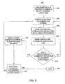
- FIG. 3 illustrates a process sequence incorporating selective deposition of a barrier layer on a metal film using a cyclical deposition process according to one embodiment described herein;
- FIG. 4 illustrates a process sequence incorporating selective deposition of a barrier layer on a metal film using a cyclical deposition process according to an alternate embodiment described herein;
- FIG. 5A is a graph showing the number of deposition cycles needed to start forming a tungsten layer on copper as compared to the number of deposition cycles needed to start forming a tungsten layer on a low dielectric constant organosilicate material;
- FIG. 5B is a graph showing the number of deposition cycles needed to start forming a tungsten layer on titanium nitride layers as compared to the number of deposition cycles needed to start forming a tungsten layer on silicon oxide;
- FIG. 5C is a graph showing the number of deposition cycles needed to start forming a tungsten layer on silicon carbide at a temperature of 300° C. and at a temperature of 350° C.;
- FIGS. 6A-6D depict cross-sectional views of a substrate at different stages of an interconnect fabrication process.
- FIG. 2 depicts a schematic cross-sectional view of a process chamber 36 that can be used to perform a cyclical deposition process in accordance with embodiments described herein.
- the process chamber 36 generally houses a wafer support pedestal 148 , which is used to support a substrate (not shown).
- the wafer support pedestal 148 is movable in a vertical direction inside the process chamber 36 using a displacement mechanism 148 a.
- the substrate can be heated to some desired temperature prior to or during deposition.
- the wafer support pedestal 148 may be heated using an embedded heater element 152 a .
- the wafer support pedestal 148 may be resistively heated by applying an electric current from an AC power supply 152 to the heater element 152 a .
- the substrate (not shown) is, in turn, heated by the pedestal 148 .
- the wafer support pedestal 148 may be heated using radiant heaters, such as, for example, lamps (not shown).
- a temperature sensor 150 a such as a thermocouple, is also embedded in the wafer support pedestal 148 to monitor the temperature of the pedestal 148 in a conventional manner. The measured temperature is used in a feedback loop to control the AC power supply 152 for the heating element 152 a , such that the substrate temperature can be maintained or controlled at a desired temperature which is suitable for the particular process application.
- a vacuum pump 118 is used to evacuate the process chamber 36 and to maintain the pressure inside the process chamber 36 .
- a gas manifold 134 through which process gases are introduced into the process chamber 36 , is located above the wafer support pedestal 148 .
- the gas manifold 134 is connected to a gas panel 111 , which controls and supplies various process gases to the process chamber 36 .
- Proper control and regulation of the gas flows to the gas manifold 134 are performed by mass flow controllers (not shown) and a microprocessor controller 154 .
- the gas manifold 134 allows process gases to be introduced and uniformly distributed in the process chamber 36 . Additionally, the gas manifold 134 may optionally be heated to prevent condensation of any reactive gases within the manifold.
- the gas manifold 134 includes a plurality of electronic control valves (not shown).
- the electronic control valves as used herein refer to any control valve capable of providing rapid and precise gas flow to the process chamber 36 with valve open and close cycles of less than about 1-2 seconds, and more preferably less than about 0.1 second.
- the microprocessor controller 154 may be one of any form of general purpose computer processor (CPU) 171 that can be used in an industrial setting for controlling various chambers and sub-processors.
- the computer may use any suitable memory 172 , such as random access memory, read only memory, floppy disk drive, hard disk, or any other form of digital storage, local or remote.
- Various support circuits 173 may be coupled to the CPU for supporting the processor in a conventional manner.
- Software routines as required may be stored in the memory or executed by a second CPU that is remotely located.
- the software routines are executed to initiate process recipes or sequences.
- the software routines when executed, transform the general purpose computer into a specific process computer that controls the chamber operation so that a chamber process is performed.
- software routines may be used to precisely control the activation of the electronic control valves for the execution of process sequences according to the present invention.
- the software routines may be performed in hardware, as an application specific integrated circuit or other type of hardware implementation, or a combination of software or hardware.
- the barrier layer may comprise a refractory metal, such as, for example, tungsten (W), among others.
- the barrier layer is selectively deposited on the metal film using a cyclical deposition process including a predetermined number of deposition cycles followed by a purge step.
- each deposition cycle comprises alternately adsorbing a refractory metal-containing precursor and a reducing gas on the metal film formed on the substrate in a process chamber.
- the refractory metal-containing precursor and the reducing gas react to form the barrier layer on the metal film.
- the process chamber is purged of both the refractory metal-containing precursor and the reducing gas. This deposition sequence of performing a predetermined number of deposition cycles followed by a process chamber purge may be repeated until a desired barrier layer is achieved.
- the predetermined number of deposition cycles is selected to take advantage of differences in the number of deposition cycles needed to start depositing the barrier material on different types of material layers.
- the predetermined number of deposition cycles is advantageously selected to start deposition of the barrier material on the metal film, but be less than the number of deposition cycles needed to start deposition of such barrier material on layers surrounding the metal film.
- barrier material is only deposited on the metal film without being deposited on any surrounding material layers.
- FIG. 3 illustrates a process sequence 200 according to the present invention detailing the various steps used for the selective deposition of a barrier layer on a metal film utilizing a constant carrier gas flow. These steps may be performed in a process chamber similar to that described above with reference to FIG. 2 .
- a substrate is introduced into a process chamber.
- the substrate may be, for example, a silicon substrate having thereon one or more copper features surrounded by insulating material.
- the process chamber conditions such as, for example, the temperature and pressure are adjusted to enhance the selective deposition of the barrier material on the metal film and impede nucleation of the barrier material on the insulating material.
- a carrier gas stream is established within the process chamber, as indicated in step 204 .
- Carrier gases may be selected so as to also act as a purge gas for removal of volatile reactants and/or by-products from the process chamber.
- Carrier gases such as, for example, helium (He), argon (Ar), nitrogen (N 2 ) and hydrogen (H 2 ), as well as combinations thereof, among others, may be used.
- a pulse of a refractory metal-containing precursor is added to the carrier gas stream.
- the term pulse as used herein refers to a dose of material injected into the process chamber or into the carrier gas stream.
- the pulse may comprise one injection of the refractory metal-containing precursor or several short, sequential injections.
- the pulse of the refractory metal-containing precursor lasts for a predetermined time interval.
- suitable tungsten-containing precursors may include, for example, tungsten hexafluoride (WF 6 ) and tungsten hexacarbonyl (W(CO) 6 ), among others.
- the time interval for the pulse of the refractory metal-containing precursor is variable depending on a number of factors such as, for example, the volume capacity of the process chamber employed, the vacuum system coupled thereto and the volatility/reactivity of the reactants used.
- the process conditions are advantageously selected so that at least a monolayer of the refractory metal-containing precursor may be adsorbed on the metal film, without adsorption of the refractory metal-containing precursor on surrounding insulating material. Thereafter, excess refractory metal-containing precursor remaining in the process chamber may be removed therefrom by the constant carrier gas stream in combination with the vacuum system.
- step 208 after the excess refractory metal-containing precursor has been sufficiently removed from the process chamber by the carrier gas stream to prevent co-reaction or particle formation with a subsequently provided process gas, a pulse of a reducing gas is added to the carrier gas stream.
- suitable reducing gases may include, for example, silane (SiH 4 ), disilane (Si 2 H 6 ), dichlorosilane (SiCl 2 H 2 ), borane (BH 3 ), diborane (B 2 H 6 ), triborane, tetraborane, pentaborane, hexaborane, heptaborane, octaborane, nanoborane and decaborane, among others.
- the pulse of the reducing gas also lasts for a predetermined time interval.
- the time interval for the pulse of the reducing gas should be long enough to provide a sufficient amount of the reducing gas for reaction with the refractory metal-containing precursor that is already adsorbed on the metal film. Thereafter, excess reducing gas is flushed from the process chamber by the carrier gas stream in combination with the vacuum system.
- Steps 204 through 208 comprise one embodiment of a deposition cycle for the barrier layer.
- a constant flow of the carrier gas is provided to the process chamber modulated by alternating periods of pulsing and non-pulsing where the periods of pulsing alternate between the refractory metal-containing precursor and the reducing gas along with the carrier gas stream, while the periods of non-pulsing include only the carrier gas stream.
- the time interval for each of the pulses of the refractory metal-containing precursor and the reducing gas may have the same duration. That is, the duration of the pulse of the refractory metal-containing precursor may be identical to the duration of the pulse of the reducing gas.
- a time interval (T 1 ) for the pulse of the refractory metal-containing precursor is equal to a time interval (T 2 ) for the pulse of the reducing gas.
- the time interval for each of the pulses of the refractory metal-containing precursor and the reducing gas may have different durations. That is, the duration of the pulse of the refractory metal-containing precursor may be shorter or longer than the duration of the pulse of the reducing gas.
- the time interval (T 1 ) for the pulse of the refractory metal-containing precursor is different than the time interval (T 2 ) for the pulse of the reducing gas.
- the periods of non-pulsing between each of the pulses of the refractory metal-containing precursor and the reducing gas may have the same duration. That is, the duration of the period of non-pulsing between each pulse of the refractory metal-containing precursor and each pulse of the reducing gas may be identical.
- a time interval (T 3 ) of non-pulsing between the pulse of the refractory metal-containing precursor and the pulse of the reducing gas is equal to a time interval (T 4 ) of non-pulsing between the pulse of the reducing gas and the pulse of the refractory metal-containing precursor.
- the periods of non-pulsing between each of the pulses of the refractory metal-containing precursor and the reducing gas may have different durations. That is, the duration of the period of non-pulsing between each pulse of the refractory metal-containing precursor and each pulse of the reducing gas may be shorter or longer than the duration of the period of non-pulsing between each pulse of the reducing gas and each pulse of the refractory metal-containing precursor.
- a time interval (T 3 ) of non-pulsing between the pulse of the refractory metal-containing precursor and the pulse of the reducing gas is different from a time interval (T 4 ) of non-pulsing between the pulse of the reducing gas and the pulse of the refractory metal-containing precursor.
- time intervals for each pulse of the refractory metal-containing precursor, the reducing gas and the periods of non-pulsing therebetween for each deposition cycle may have the same duration.
- a time interval (T 1 ) for the pulse of the refractory metal-containing precursor may have the same duration as the time interval (T 1 ) for the pulse of the refractory metal-containing precursor in subsequent deposition cycles (C 2 . . . C N ).
- each pulse of the reducing gas as well as the periods of non-pulsing between the pulses of the refractory metal-containing precursor and the reducing gas in the first deposition cycle (C 1 ) may have the same duration as each pulse of the reducing gas and the periods of non-pulsing between the pulses of the refractory metal-containing precursor and the reducing gas in subsequent deposition cycles (C 2 . . . C N ), respectively.
- the time interval for at least one pulse of the refractory metal-containing precursor, the reducing gas and the periods of non-pulsing therebetween for one or more of the deposition cycles of the barrier layer deposition process may have different durations.
- the time interval (T 1 ) for the pulse of the refractory metal-containing precursor may be longer or shorter than the time interval (T 1 ) for the pulse of the refractory metal-containing precursor in subsequent deposition cycles (C 2 . . . C N ).
- the duration of one or more pulse of the reducing gas or the periods of non-pulsing between the pulses of the refractory metal-containing precursor and the reducing gas in deposition cycle (C 1 ) may be longer or shorter than the duration of corresponding pulses of the reducing gas or the periods of non-pulsing between the pulses of the refractory metal-containing precursor and the reducing gas in subsequent deposition cycles (C 2 . . . C N ), respectively.
- step 210 after each deposition cycle (steps 204 through 208 ), the total number of deposition cycles performed is determined. If a predetermined number of deposition cycles have not been performed, steps 204 through 208 are repeated until such predetermined number of deposition cycles, have been completed. However, if a predetermined number of deposition cycles have been completed, the process chamber is purged of both the refractory metal-containing precursor and the reducing gas, as indicated by step 212 . The process chamber may be purged using the carrier gas stream. After the process chamber is purged, additional predetermined numbers of deposition cycles (steps 204 through 208 ) may be performed until a desired thickness for the barrier layer is achieved as indicated by step 214 , or ended as indicated by step 216 .
- the predetermined number of deposition cycles is selected to start depositing barrier material on the metal film within the first few deposition cycles, but be less than the number of deposition cycles needed to start depositing such barrier material on the surrounding insulating material layer. Limiting the number of deposition cycles to a predetermined number that is less than the number needed to start deposition of barrier material on the surrounding insulating material and than purging the process chamber, permits selective deposition of the barrier material only on the metal film.
- a barrier layer deposition sequence 300 includes introducing a substrate into the process chamber (step 302 ), providing a pulse of a carrier gas to the process chamber (step 304 ), providing a pulse of a refractory metal-containing precursor to the process chamber (step 306 ), providing a pulse of a carrier gas to the process chamber (step 308 ), providing a pulse of a reducing gas to the process chamber (step 310 ), and repeating steps 304 through 310 until a predetermined number of deposition cycles are performed (step 312 ).
- the process chamber is purged of both the refractory metal-containing precursor and the reducing gas (step 314 ).
- additional predetermined numbers of deposition cycles may be performed until a desired thickness for the barrier layer is achieved (step 316 ), or ended (step 318 ).
- the time intervals for each of the pulses of the refractory metal-containing precursor, the reducing gas and the carrier gas may have the same or different durations as discussed above with respect to FIG. 3 .
- corresponding time intervals for one or more pulses of the refractory metal-containing precursor, the reducing gas and the carrier gas in one or more of the deposition cycles of the barrier layer deposition process may have different durations.
- the barrier layer deposition cycle is depicted as beginning with a pulse of the refractory metal-containing precursor followed by a pulse of the reducing gas.
- the barrier layer deposition cycle may start with a pulse of the reducing gas followed by a pulse of the refractory metal-containing precursor.
- a pulse may comprise one injection of a gas or several short, sequential injections.
- One exemplary deposition cycle for selectively forming a tungsten barrier layer on copper features that are surrounded by organosilicate insulating material comprises sequentially providing pulses of silane (SiH 4 ) and pulses of tungsten hexafluoride (WF 6 ) to a process chamber similar to that described above with reference to FIG. 2 .
- argon (Ar) may be provided to an appropriate flow control valve, for example an electronic flow control valve, at a flow rate of between about 100 sccm (standard cubic centimeters per second) to about 1000 sccm, preferably at about 300 sccm, and thereafter pulsed for about 100 msec (milliseconds) to about 1000 msec, preferably for about 500 msec.
- an appropriate flow control valve for example an electronic flow control valve
- the silane (SiH 4 ) may be provided to an appropriate flow control valve, for example an electronic flow control valve, at a flow rate of between about 10 sccm to about 200 sccm, preferably at about 20 sccm, and thereafter pulsed for about 100 msec to about 1000 msec, preferably for about 500 msec.
- a carrier gas comprising hydrogen (H 2 ) may be provided along with the silane (SiH 4 ) at a flow rate of between about 100 sccm to about 1000 sccm, preferably at about 300 sccm.
- Argon is than provided at a flow rate of between about 100 sccm (standard cubic centimeters per second) to about 1000 sccm, preferably at about 300 sccm, and thereafter pulsed for about 100 msec (milliseconds) to about 1000 msec, preferably for about 500 msec.
- the tungsten hexafluoride (WF 6 ) may be provided to an appropriate flow control valve, for example an electronic flow control valve, at a flow rate of between about 10 sccm to about 100 sccm, preferably at about 30 sccm, and thereafter pulsed for about 100 msec to about 1000 msec, preferably for about 500 msec.
- a carrier gas comprising argon (Ar) may be provided along with the tungsten hexafluoride (WF 6 ) at a flow rate of between about 100 sccm to about 1000 sccm, preferably at about 300 sccm.
- the substrate may be maintained at a temperature between about 250° C. to about 375° C., preferably at about 300° C., at a chamber pressure of about 1 torr to about 40 torr, preferably at about 5 torr.
- the process chamber is purged by providing a flow of the carrier gas thereto.
- Gases such as for example, argon (Ar), helium (He), nitrogen (N 2 ) and hydrogen (H 2 ), among others may be used.
- the process chamber may be purged by providing a flow of gas at about 300 sccm to about 1000 sccm, preferably at about 600 sccm, for a duration of up to about 2 seconds, preferably for about 0.3 seconds.
- FIG. 5A is a plot illustrating the number of deposition cycles needed to start forming a tungsten layer on copper as compared to the number of deposition cycles needed to start forming a tungsten layer on a low dielectric constant organosilicate material (dielectric constant less than about 3.5).
- Each deposition cycle was performed at a substrate temperature of about 300° C., a deposition chamber pressure of about 5 torr, a silane (SiH 4 ) flow of about 20 sccm with a hydrogen (H 2 ) carrier flow of 300 sccm that is pulsed for about 500 msec, a tungsten hexafluoride (WF 6 ) flow of about 30 sccm with an argon (Ar) flow of about 300 sccm that is pulsed for about 500 msec, and an argon (Ar) flow of about 300 sccm for about 500 msec between each pulse of the silane (SiH 4 ) and each pulse of the tungsten hexafluoride (WF 6 ).
- tungsten starts to deposit on the copper during a first deposition cycle, as indicated by line 400 .
- the tungsten starts to deposit on the low dielectric constant organosilicate material during the fourth deposition cycle, as indicated by line 405 .
- selective deposition of tungsten on copper without deposition on the organosilicate material necessitates that the process chamber be purged each time three deposition cycles have been completed.
- FIG. 5B is a plot illustrating the number of deposition cycles needed to start forming a tungsten layer on a titanium nitride layer deposited using a physical vapor deposition (PVD) process, a titanium nitride layer deposited from a metallorganic precursor in a chemical vapor deposition (MOCVD) process, or a titanium nitride layer deposited from a titanium tetrachloride (TiCl 4 ) precursor in a chemical vapor deposition (CVD) process as compared to the number of deposition cycles needed to start forming a tungsten layer on silicon oxide material.
- PVD physical vapor deposition
- MOCVD chemical vapor deposition
- TiCl 4 titanium tetrachloride
- Each deposition cycle was performed at a substrate temperature of about 300° C., a deposition chamber pressure of about 5 torr, a silane (SiH 4 ) flow of about 20 sccm with a hydrogen (H 2 ) carrier flow of 300 sccm that is pulsed for about 500 msec, a tungsten hexafluoride (WF 6 ) flow of about 30 sccm with an argon (Ar) flow of about 300 sccm that is pulsed for about 500 msec, and an argon (Ar) flow of about 300 sccm for about 500 msec between each pulse of the silane (SiH 4 ) and each pulse of the tungsten hexafluoride (WF 6 ).
- tungsten starts to deposit on the titanium nitride layer deposited from a metallorganic precursor using a chemical vapor deposition (MOCVD) process during a first deposition cycle, as indicated by line 410 .
- MOCVD chemical vapor deposition
- Tungsten starts to deposit on the titanium nitride layer deposited using a physical vapor deposition (PVD) process, or a titanium nitride layer deposited from a titanium tetrachloride (TiCl 4 ) precursor using a chemical vapor deposition (CVD) during a second deposition cycle, as indicated by lines 415 , 420 , respectively.
- the tungsten starts to deposit on the silicon oxide during the seventh deposition cycle, as indicated by line 425 .
- the number of deposition cycles needed to start forming a tungsten layer on an dielectric insulating material may vary as a function of the substrate temperature.
- a tungsten layer was formed on silicon carbide at a substrate temperature of about 300° C. and a substrate temperature of about 350° C.
- Each deposition cycle was performed at a deposition chamber pressure of about 5 torr, a silane (SiH 4 ) flow of about 20 sccm with a hydrogen (H 2 ) carrier flow of 300 sccm that is pulsed for about 500 msec, a tungsten hexafluoride (WF 6 ) flow of about 30 sccm with an argon (Ar) flow of about 300 sccm that is pulsed for about 500 msec, and an argon (Ar) flow of about 300 sccm for about 500 msec between each pulse of the silane (SiH 4 ) and each pulse of the tungsten hexafluoride (WF 6 ).
- FIGS. 6A-6D illustrate schematic cross-sectional views of a substrate 500 at different stages of an integrated circuit fabrication sequence incorporating a tungsten barrier layer formed on conductive leads.
- substrate 500 may correspond to a silicon substrate, or other material layer that has been formed on the substrate 500 .
- FIG. 6A illustrates a cross-sectional view of a substrate 500 having conductive leads formed thereon surrounded by a dielectric material.
- the conductive leads 501 may be a metal (e.g., aluminum (Al) or copper (Cu)).
- the dielectric material 502 may be an oxide (silicon oxide) as well as low dielectric constant materials such as BLACK DIAMONDTM, or other insulating materials with dielectric constants less than 3.5.
- FIG. 6A illustrates one embodiment in which the substrate 500 is silicon having copper leads 501 formed thereon.
- the copper leads 501 have a thickness of about 5,000 ⁇ to about 5 microns depending on the size of the structure to be fabricated.
- a dielectric material 502 surrounds the copper leads 501 .
- the dielectric material 502 may be a low dielectric constant silicon oxide layer.
- the dielectric material 502 has a thickness corresponding to the thickness of the copper leads 501 .
- a tungsten barrier layer 503 is selectively formed on the copper leads 501 .
- the tungsten barrier layer 503 may be formed according to the process parameters described above with respect to FIGS. 3-4.
- the thickness of the tungsten barrier layer 503 should be about 30 ⁇ to about 50 ⁇ . Formation of the tungsten barrier layer 503 on the copper leads 501 advantageously eliminates the need for the deposition of a, dielectric barrier material such as for example, silicon carbide, thereover.
- a bulk-insulating layer 506 is formed on the tungsten barrier layer 503 and the dielectric material 502 .
- the bulk-insulating layer 506 may be a silicon oxide formed as is well known in the art.
- the bulk-insulating layer should have a thickness of about 5,000 ⁇ to about 10,000 ⁇ .
- vias 509 are defined in the bulk-insulating layer 506 over the copper leads 501 .
- the vias 509 are defined in the bulk-insulating layer 506 using conventional lithography and etching techniques.
- the vias 509 are filled with a conductive material 516 such as aluminum (Al), copper (Cu), tungsten (W), or combinations thereof.
- a conductive material 516 such as aluminum (Al), copper (Cu), tungsten (W), or combinations thereof.
- copper (Cu) is used to fill the vias 509 due to its low resistivity (resistivity of about 1.7 ⁇ /cm).
- the conductive material 516 may be deposited using chemical vapor deposition (CVD) techniques, physical vapor deposition (PVD) techniques, electroplating techniques, or combinations thereof.
- a barrier layer 518 such as tantalum (Ta), tantalum nitride (TaN), titanium (Ti), titanium nitride (TiN), or other suitable barrier material may be deposited conformably on vias 509 , before filling them with the conductive material 516 .
- the barrier layer 518 functions to prevent metal migration into the bulk-insulating layer 506 .
Abstract
A method to selectively deposit a barrier layer on a metal film formed on a substrate is disclosed. The barrier layer is selectively deposited on the metal film using a cyclical deposition process including a predetermined number of deposition cycles followed by a purge step. Each deposition cycle comprises alternately adsorbing a refractory metal-containing precursor and a reducing gas on the metal film formed on the substrate in a process chamber.
Description
This application claims benefit of U.S. provisional patent application Ser. No. 60/342,225, filed on Dec. 21, 2001, which is incorporated by reference in its entirety.
1. Field of the Invention
Embodiments of the present invention relate generally to a method of tungsten layer formation.
2. Description of the Related Art
Integrated circuits have evolved into complex devices that can include millions of components (e.g., transistors, capacitors and resistors) on a single chip. The evolution of chip designs continually requires faster circuitry and greater circuit densities. The demand for greater circuit densities necessitates a reduction in the dimensions of the integrated circuit components.
As the dimensions of the integrated circuit components are reduced (e.g., sub-micron dimensions), the materials used to fabricate such components contribute to the electrical performance thereof. For example, low resistivity metal interconnects (e.g., aluminum (Al) and copper (Cu)) provide conductive paths between the components on integrated circuits.
Referring to FIG. 1, the metal interconnects 2 are typically electrically isolated from each other by a bulk insulating material 4. When the distance between adjacent metal interconnects 2 and/or the thickness of the bulk insulating material 4 has sub-micron dimensions, capacitive coupling potentially occurs between such interconnects 2. Capacitive coupling between adjacent metal interconnects 2 may cause cross-talk and/or resistance-capacitance (RC) delay, which degrades the overall performance of the integrated circuit.
In order to minimize capacitive coupling between adjacent metal interconnects, low dielectric constant bulk insulating materials 4 (e.g., dielectric constants less than about 3.5) are used. Examples of low dielectric constant bulk insulating materials include silicon dioxide (SiO2), silicate glass and organosilicates, among others.
In addition, a barrier layer 6 is typically formed over the metal interconnects 2 as well as the bulk insulating material 4. The barrier layer 6 minimizes the diffusion of the metal from the metal interconnects 2 into a subsequently deposited insulating material layer 8. Diffusion of the metal from the metal interconnects 2 into the subsequently deposited insulating material layer 8 is undesirable because such diffusion can affect the electrical performance of the integrated circuit (e.g., cross-talk and or RC delay) or render it inoperable.
Silicon carbide is often used for the barrier layer 6. However, silicon carbide has a dielectric constant of about 4.0 to about 5.0. The dielectric constant of the silicon carbide in conjunction with the dielectric constant of the bulk insulating materials tends to increase the overall dielectric constant of the metal interconnect structure which may degrade the performance of the integrated circuit.
Thus, a need exists for a method to selectively deposit a barrier layer on a metal film.
A method to selectively deposit a barrier layer on a metal film formed on a substrate is described. The barrier layer may comprise a refractory metal such as, for example, tungsten (W). The barrier layer is selectively deposited on the metal film using a cyclical deposition process including a predetermined number of deposition cycles followed by a purge step.
In the cyclical deposition process, each deposition cycle comprises alternately adsorbing a refractory metal-containing precursor and a reducing gas on the metal film formed on the substrate in a process chamber. The refractory metal-containing precursor and the reducing gas react to form the barrier layer on the metal film. After a predetermined number of deposition cycles are completed, the process chamber is purged of both the refractory metal-containing precursor and the reducing gas. This deposition sequence of performing a predetermined number of deposition cycles followed by a process chamber purge may be repeated until a desired barrier layer thickness is achieved.
The predetermined number of deposition cycles is selected to take advantage of differences in the number of deposition cycles needed to start depositing the barrier material on different types of material layers. Thus, the predetermined number of deposition cycles is advantageously selected to start deposition of the barrier material on the metal film but be less than the number of deposition cycles needed to start deposition of such barrier material on layers surrounding the metal film. As such, barrier material is only deposited on the metal film without being deposited on any surrounding material layers.
The selective deposition of the barrier layer is compatible with integrated circuit fabrication processes. In one integrated circuit fabrication process, the barrier layer is used as a cap layer for a metal feature in a damascene structure. For such an embodiment, a preferred process sequence includes providing a substrate having metal features formed thereon that are surrounded by a dielectric oxide. A barrier layer is selectively deposited on the metal features using a cyclical deposition process in which a predetermined number of deposition cycles, each comprising alternately adsorbing a refractory metal-containing precursor and a reducing gas on the metal features, is followed by a process chamber purge step. The cyclical deposition process is repeated until a desired thickness for the barrier layer is achieved. After the barrier layer is selectively deposited on the metal features, one or more insulating layers are formed thereon and patterned to define vias therethrough to the barrier layer formed on the metal features. Thereafter, the damascene structure is completed by filling the vias with a conductive material.
So that the manner in which the above recited features of the present invention are attained and can be understood in detail, a more particular description of the invention, briefly summarized above, may be had by reference to the embodiments thereof which are illustrated in the appended drawings.
It is to be noted, however, that the appended drawings illustrate only typical embodiments of this invention and are therefore not to be considered limiting of its scope, for the invention may admit to other equally effective embodiments.
FIG. 1 is a cross-sectional view of a metal interconnect structure including a barrier layer formed over both metal interconnects and bulk insulating material;
FIG. 2 depicts a schematic cross-sectional view of a process chamber that can be used to perform a cyclical deposition process as described herein;
FIG. 3 illustrates a process sequence incorporating selective deposition of a barrier layer on a metal film using a cyclical deposition process according to one embodiment described herein;
FIG. 4 illustrates a process sequence incorporating selective deposition of a barrier layer on a metal film using a cyclical deposition process according to an alternate embodiment described herein;
FIG. 5A is a graph showing the number of deposition cycles needed to start forming a tungsten layer on copper as compared to the number of deposition cycles needed to start forming a tungsten layer on a low dielectric constant organosilicate material;
FIG. 5B is a graph showing the number of deposition cycles needed to start forming a tungsten layer on titanium nitride layers as compared to the number of deposition cycles needed to start forming a tungsten layer on silicon oxide;
FIG. 5C is a graph showing the number of deposition cycles needed to start forming a tungsten layer on silicon carbide at a temperature of 300° C. and at a temperature of 350° C.; and
FIGS. 6A-6D depict cross-sectional views of a substrate at different stages of an interconnect fabrication process.
FIG. 2 depicts a schematic cross-sectional view of a process chamber 36 that can be used to perform a cyclical deposition process in accordance with embodiments described herein. The process chamber 36 generally houses a wafer support pedestal 148, which is used to support a substrate (not shown). The wafer support pedestal 148 is movable in a vertical direction inside the process chamber 36 using a displacement mechanism 148 a.
Depending on the specific process, the substrate can be heated to some desired temperature prior to or during deposition. For example, the wafer support pedestal 148 may be heated using an embedded heater element 152 a. The wafer support pedestal 148 may be resistively heated by applying an electric current from an AC power supply 152 to the heater element 152 a. The substrate (not shown) is, in turn, heated by the pedestal 148. Alternatively, the wafer support pedestal 148 may be heated using radiant heaters, such as, for example, lamps (not shown).
A temperature sensor 150 a, such as a thermocouple, is also embedded in the wafer support pedestal 148 to monitor the temperature of the pedestal 148 in a conventional manner. The measured temperature is used in a feedback loop to control the AC power supply 152 for the heating element 152 a, such that the substrate temperature can be maintained or controlled at a desired temperature which is suitable for the particular process application.
A vacuum pump 118 is used to evacuate the process chamber 36 and to maintain the pressure inside the process chamber 36. A gas manifold 134, through which process gases are introduced into the process chamber 36, is located above the wafer support pedestal 148. The gas manifold 134 is connected to a gas panel 111, which controls and supplies various process gases to the process chamber 36.
Proper control and regulation of the gas flows to the gas manifold 134 are performed by mass flow controllers (not shown) and a microprocessor controller 154. The gas manifold 134 allows process gases to be introduced and uniformly distributed in the process chamber 36. Additionally, the gas manifold 134 may optionally be heated to prevent condensation of any reactive gases within the manifold.
The gas manifold 134 includes a plurality of electronic control valves (not shown). The electronic control valves as used herein refer to any control valve capable of providing rapid and precise gas flow to the process chamber 36 with valve open and close cycles of less than about 1-2 seconds, and more preferably less than about 0.1 second.
The microprocessor controller 154 may be one of any form of general purpose computer processor (CPU) 171 that can be used in an industrial setting for controlling various chambers and sub-processors. The computer may use any suitable memory 172, such as random access memory, read only memory, floppy disk drive, hard disk, or any other form of digital storage, local or remote. Various support circuits 173 may be coupled to the CPU for supporting the processor in a conventional manner. Software routines as required may be stored in the memory or executed by a second CPU that is remotely located.
The software routines are executed to initiate process recipes or sequences. The software routines, when executed, transform the general purpose computer into a specific process computer that controls the chamber operation so that a chamber process is performed. For example, software routines may be used to precisely control the activation of the electronic control valves for the execution of process sequences according to the present invention. Alternatively, the software routines may be performed in hardware, as an application specific integrated circuit or other type of hardware implementation, or a combination of software or hardware.
Selective Barrier Layer Deposition on a Metal Film
A method to selectively deposit a barrier layer on a metal film formed on a substrate is described. The barrier layer may comprise a refractory metal, such as, for example, tungsten (W), among others. The barrier layer is selectively deposited on the metal film using a cyclical deposition process including a predetermined number of deposition cycles followed by a purge step.
In the cyclical deposition process, each deposition cycle comprises alternately adsorbing a refractory metal-containing precursor and a reducing gas on the metal film formed on the substrate in a process chamber. The refractory metal-containing precursor and the reducing gas react to form the barrier layer on the metal film. After a predetermined number of deposition cycles are completed, the process chamber is purged of both the refractory metal-containing precursor and the reducing gas. This deposition sequence of performing a predetermined number of deposition cycles followed by a process chamber purge may be repeated until a desired barrier layer is achieved.
The predetermined number of deposition cycles is selected to take advantage of differences in the number of deposition cycles needed to start depositing the barrier material on different types of material layers. Thus, the predetermined number of deposition cycles is advantageously selected to start deposition of the barrier material on the metal film, but be less than the number of deposition cycles needed to start deposition of such barrier material on layers surrounding the metal film. As such, barrier material is only deposited on the metal film without being deposited on any surrounding material layers.
FIG. 3 illustrates a process sequence 200 according to the present invention detailing the various steps used for the selective deposition of a barrier layer on a metal film utilizing a constant carrier gas flow. These steps may be performed in a process chamber similar to that described above with reference to FIG. 2. As indicated in step 202, a substrate is introduced into a process chamber. The substrate may be, for example, a silicon substrate having thereon one or more copper features surrounded by insulating material. The process chamber conditions such as, for example, the temperature and pressure are adjusted to enhance the selective deposition of the barrier material on the metal film and impede nucleation of the barrier material on the insulating material.
In one embodiment where a constant carrier gas flow is desired, a carrier gas stream is established within the process chamber, as indicated in step 204. Carrier gases may be selected so as to also act as a purge gas for removal of volatile reactants and/or by-products from the process chamber. Carrier gases such as, for example, helium (He), argon (Ar), nitrogen (N2) and hydrogen (H2), as well as combinations thereof, among others, may be used.
Referring to step 206, after the carrier gas stream is established within the process chamber, a pulse of a refractory metal-containing precursor is added to the carrier gas stream. The term pulse as used herein refers to a dose of material injected into the process chamber or into the carrier gas stream. The pulse may comprise one injection of the refractory metal-containing precursor or several short, sequential injections. The pulse of the refractory metal-containing precursor lasts for a predetermined time interval. When the barrier layer comprises tungsten (W), suitable tungsten-containing precursors may include, for example, tungsten hexafluoride (WF6) and tungsten hexacarbonyl (W(CO)6), among others.
The time interval for the pulse of the refractory metal-containing precursor is variable depending on a number of factors such as, for example, the volume capacity of the process chamber employed, the vacuum system coupled thereto and the volatility/reactivity of the reactants used. In general, the process conditions are advantageously selected so that at least a monolayer of the refractory metal-containing precursor may be adsorbed on the metal film, without adsorption of the refractory metal-containing precursor on surrounding insulating material. Thereafter, excess refractory metal-containing precursor remaining in the process chamber may be removed therefrom by the constant carrier gas stream in combination with the vacuum system.
In step 208, after the excess refractory metal-containing precursor has been sufficiently removed from the process chamber by the carrier gas stream to prevent co-reaction or particle formation with a subsequently provided process gas, a pulse of a reducing gas is added to the carrier gas stream. When the barrier layer comprises tungsten (W) suitable reducing gases may include, for example, silane (SiH4), disilane (Si2H6), dichlorosilane (SiCl2H2), borane (BH3), diborane (B2H6), triborane, tetraborane, pentaborane, hexaborane, heptaborane, octaborane, nanoborane and decaborane, among others.
The pulse of the reducing gas also lasts for a predetermined time interval. In general, the time interval for the pulse of the reducing gas should be long enough to provide a sufficient amount of the reducing gas for reaction with the refractory metal-containing precursor that is already adsorbed on the metal film. Thereafter, excess reducing gas is flushed from the process chamber by the carrier gas stream in combination with the vacuum system.
The time interval for each of the pulses of the refractory metal-containing precursor and the reducing gas may have the same duration. That is, the duration of the pulse of the refractory metal-containing precursor may be identical to the duration of the pulse of the reducing gas. For such an embodiment, a time interval (T1) for the pulse of the refractory metal-containing precursor is equal to a time interval (T2) for the pulse of the reducing gas.
Alternatively, the time interval for each of the pulses of the refractory metal-containing precursor and the reducing gas may have different durations. That is, the duration of the pulse of the refractory metal-containing precursor may be shorter or longer than the duration of the pulse of the reducing gas. For such an embodiment, the time interval (T1) for the pulse of the refractory metal-containing precursor is different than the time interval (T2) for the pulse of the reducing gas.
In addition, the periods of non-pulsing between each of the pulses of the refractory metal-containing precursor and the reducing gas may have the same duration. That is, the duration of the period of non-pulsing between each pulse of the refractory metal-containing precursor and each pulse of the reducing gas may be identical. For such an embodiment, a time interval (T3) of non-pulsing between the pulse of the refractory metal-containing precursor and the pulse of the reducing gas is equal to a time interval (T4) of non-pulsing between the pulse of the reducing gas and the pulse of the refractory metal-containing precursor. During the time periods of non-pulsing only the constant carrier gas stream is provided to the process chamber.
Alternatively, the periods of non-pulsing between each of the pulses of the refractory metal-containing precursor and the reducing gas may have different durations. That is, the duration of the period of non-pulsing between each pulse of the refractory metal-containing precursor and each pulse of the reducing gas may be shorter or longer than the duration of the period of non-pulsing between each pulse of the reducing gas and each pulse of the refractory metal-containing precursor. For such an embodiment, a time interval (T3) of non-pulsing between the pulse of the refractory metal-containing precursor and the pulse of the reducing gas is different from a time interval (T4) of non-pulsing between the pulse of the reducing gas and the pulse of the refractory metal-containing precursor. During the periods of non-pulsing only the constant carrier gas stream is provided to the process chamber.
Additionally, the time intervals for each pulse of the refractory metal-containing precursor, the reducing gas and the periods of non-pulsing therebetween for each deposition cycle may have the same duration. For example, in a first deposition cycle (C1), a time interval (T1) for the pulse of the refractory metal-containing precursor may have the same duration as the time interval (T1) for the pulse of the refractory metal-containing precursor in subsequent deposition cycles (C2 . . . CN). Similarly, the duration of each pulse of the reducing gas as well as the periods of non-pulsing between the pulses of the refractory metal-containing precursor and the reducing gas in the first deposition cycle (C1) may have the same duration as each pulse of the reducing gas and the periods of non-pulsing between the pulses of the refractory metal-containing precursor and the reducing gas in subsequent deposition cycles (C2 . . . CN), respectively.
Alternatively, the time interval for at least one pulse of the refractory metal-containing precursor, the reducing gas and the periods of non-pulsing therebetween for one or more of the deposition cycles of the barrier layer deposition process may have different durations. For example, in a first deposition cycle (C1), the time interval (T1) for the pulse of the refractory metal-containing precursor may be longer or shorter than the time interval (T1) for the pulse of the refractory metal-containing precursor in subsequent deposition cycles (C2 . . . CN). Similarly, the duration of one or more pulse of the reducing gas or the periods of non-pulsing between the pulses of the refractory metal-containing precursor and the reducing gas in deposition cycle (C1) may be longer or shorter than the duration of corresponding pulses of the reducing gas or the periods of non-pulsing between the pulses of the refractory metal-containing precursor and the reducing gas in subsequent deposition cycles (C2 . . . CN), respectively.
Referring to step 210, after each deposition cycle (steps 204 through 208), the total number of deposition cycles performed is determined. If a predetermined number of deposition cycles have not been performed, steps 204 through 208 are repeated until such predetermined number of deposition cycles, have been completed. However, if a predetermined number of deposition cycles have been completed, the process chamber is purged of both the refractory metal-containing precursor and the reducing gas, as indicated by step 212. The process chamber may be purged using the carrier gas stream. After the process chamber is purged, additional predetermined numbers of deposition cycles (steps 204 through 208) may be performed until a desired thickness for the barrier layer is achieved as indicated by step 214, or ended as indicated by step 216.
For a particular barrier material, the predetermined number of deposition cycles is selected to start depositing barrier material on the metal film within the first few deposition cycles, but be less than the number of deposition cycles needed to start depositing such barrier material on the surrounding insulating material layer. Limiting the number of deposition cycles to a predetermined number that is less than the number needed to start deposition of barrier material on the surrounding insulating material and than purging the process chamber, permits selective deposition of the barrier material only on the metal film.
In an alternate process sequence described with respect to FIG. 4, the barrier layer deposition cycle may comprise separate pulses for each of the refractory metal-containing precursor, the reducing gas and the carrier gas. For such an embodiment, a barrier layer deposition sequence 300 includes introducing a substrate into the process chamber (step 302), providing a pulse of a carrier gas to the process chamber (step 304), providing a pulse of a refractory metal-containing precursor to the process chamber (step 306), providing a pulse of a carrier gas to the process chamber (step 308), providing a pulse of a reducing gas to the process chamber (step 310), and repeating steps 304 through 310 until a predetermined number of deposition cycles are performed (step 312). When a predetermined number of deposition cycles have been completed, the process chamber is purged of both the refractory metal-containing precursor and the reducing gas (step 314). After the process chamber is purged, additional predetermined numbers of deposition cycles (steps 304 through 310) may be performed until a desired thickness for the barrier layer is achieved (step 316), or ended (step 318).
The time intervals for each of the pulses of the refractory metal-containing precursor, the reducing gas and the carrier gas may have the same or different durations as discussed above with respect to FIG. 3. Alternatively, corresponding time intervals for one or more pulses of the refractory metal-containing precursor, the reducing gas and the carrier gas in one or more of the deposition cycles of the barrier layer deposition process may have different durations.
In FIGS. 3-4, the barrier layer deposition cycle is depicted as beginning with a pulse of the refractory metal-containing precursor followed by a pulse of the reducing gas. Alternatively, the barrier layer deposition cycle may start with a pulse of the reducing gas followed by a pulse of the refractory metal-containing precursor. In addition, a pulse may comprise one injection of a gas or several short, sequential injections.
One exemplary deposition cycle for selectively forming a tungsten barrier layer on copper features that are surrounded by organosilicate insulating material comprises sequentially providing pulses of silane (SiH4) and pulses of tungsten hexafluoride (WF6) to a process chamber similar to that described above with reference to FIG. 2. For such a deposition cycle, argon (Ar) may be provided to an appropriate flow control valve, for example an electronic flow control valve, at a flow rate of between about 100 sccm (standard cubic centimeters per second) to about 1000 sccm, preferably at about 300 sccm, and thereafter pulsed for about 100 msec (milliseconds) to about 1000 msec, preferably for about 500 msec. The silane (SiH4) may be provided to an appropriate flow control valve, for example an electronic flow control valve, at a flow rate of between about 10 sccm to about 200 sccm, preferably at about 20 sccm, and thereafter pulsed for about 100 msec to about 1000 msec, preferably for about 500 msec. A carrier gas comprising hydrogen (H2) may be provided along with the silane (SiH4) at a flow rate of between about 100 sccm to about 1000 sccm, preferably at about 300 sccm. Argon is than provided at a flow rate of between about 100 sccm (standard cubic centimeters per second) to about 1000 sccm, preferably at about 300 sccm, and thereafter pulsed for about 100 msec (milliseconds) to about 1000 msec, preferably for about 500 msec. The tungsten hexafluoride (WF6) may be provided to an appropriate flow control valve, for example an electronic flow control valve, at a flow rate of between about 10 sccm to about 100 sccm, preferably at about 30 sccm, and thereafter pulsed for about 100 msec to about 1000 msec, preferably for about 500 msec. A carrier gas comprising argon (Ar) may be provided along with the tungsten hexafluoride (WF6) at a flow rate of between about 100 sccm to about 1000 sccm, preferably at about 300 sccm. The substrate may be maintained at a temperature between about 250° C. to about 375° C., preferably at about 300° C., at a chamber pressure of about 1 torr to about 40 torr, preferably at about 5 torr.
After a predetermined number of deposition cycles are performed, the process chamber is purged by providing a flow of the carrier gas thereto. Gases such as for example, argon (Ar), helium (He), nitrogen (N2) and hydrogen (H2), among others may be used. The process chamber may be purged by providing a flow of gas at about 300 sccm to about 1000 sccm, preferably at about 600 sccm, for a duration of up to about 2 seconds, preferably for about 0.3 seconds.
FIG. 5A is a plot illustrating the number of deposition cycles needed to start forming a tungsten layer on copper as compared to the number of deposition cycles needed to start forming a tungsten layer on a low dielectric constant organosilicate material (dielectric constant less than about 3.5). Each deposition cycle was performed at a substrate temperature of about 300° C., a deposition chamber pressure of about 5 torr, a silane (SiH4) flow of about 20 sccm with a hydrogen (H2) carrier flow of 300 sccm that is pulsed for about 500 msec, a tungsten hexafluoride (WF6) flow of about 30 sccm with an argon (Ar) flow of about 300 sccm that is pulsed for about 500 msec, and an argon (Ar) flow of about 300 sccm for about 500 msec between each pulse of the silane (SiH4) and each pulse of the tungsten hexafluoride (WF6).
Referring to FIG. 5A, tungsten starts to deposit on the copper during a first deposition cycle, as indicated by line 400. However, the tungsten starts to deposit on the low dielectric constant organosilicate material during the fourth deposition cycle, as indicated by line 405. As such, for the process conditions recited above with respect to FIG. 5A, selective deposition of tungsten on copper without deposition on the organosilicate material, necessitates that the process chamber be purged each time three deposition cycles have been completed.
FIG. 5B is a plot illustrating the number of deposition cycles needed to start forming a tungsten layer on a titanium nitride layer deposited using a physical vapor deposition (PVD) process, a titanium nitride layer deposited from a metallorganic precursor in a chemical vapor deposition (MOCVD) process, or a titanium nitride layer deposited from a titanium tetrachloride (TiCl4) precursor in a chemical vapor deposition (CVD) process as compared to the number of deposition cycles needed to start forming a tungsten layer on silicon oxide material. Each deposition cycle was performed at a substrate temperature of about 300° C., a deposition chamber pressure of about 5 torr, a silane (SiH4) flow of about 20 sccm with a hydrogen (H2) carrier flow of 300 sccm that is pulsed for about 500 msec, a tungsten hexafluoride (WF6) flow of about 30 sccm with an argon (Ar) flow of about 300 sccm that is pulsed for about 500 msec, and an argon (Ar) flow of about 300 sccm for about 500 msec between each pulse of the silane (SiH4) and each pulse of the tungsten hexafluoride (WF6).
Referring to FIG. 5B, tungsten starts to deposit on the titanium nitride layer deposited from a metallorganic precursor using a chemical vapor deposition (MOCVD) process during a first deposition cycle, as indicated by line 410. Tungsten starts to deposit on the titanium nitride layer deposited using a physical vapor deposition (PVD) process, or a titanium nitride layer deposited from a titanium tetrachloride (TiCl4) precursor using a chemical vapor deposition (CVD) during a second deposition cycle, as indicated by lines 415, 420, respectively. However, the tungsten starts to deposit on the silicon oxide during the seventh deposition cycle, as indicated by line 425. As such, for the process conditions recited above with respect to FIG. 5B, selective deposition of tungsten on either of the titanium nitride layers without deposition on the silicon oxide necessitates that the process chamber be purged each time six deposition cycles have been completed.
The number of deposition cycles needed to start forming a tungsten layer on an dielectric insulating material may vary as a function of the substrate temperature. For example, a tungsten layer was formed on silicon carbide at a substrate temperature of about 300° C. and a substrate temperature of about 350° C. Each deposition cycle was performed at a deposition chamber pressure of about 5 torr, a silane (SiH4) flow of about 20 sccm with a hydrogen (H2) carrier flow of 300 sccm that is pulsed for about 500 msec, a tungsten hexafluoride (WF6) flow of about 30 sccm with an argon (Ar) flow of about 300 sccm that is pulsed for about 500 msec, and an argon (Ar) flow of about 300 sccm for about 500 msec between each pulse of the silane (SiH4) and each pulse of the tungsten hexafluoride (WF6). Referring to FIG. 5C, ten deposition cycles were needed to start forming a tungsten layer on silicon carbide at a substrate temperature of about 300° C., as indicated by line 430. In contrast, only five deposition cycles were needed to start forming a tungsten layer on silicon carbide when the substrate temperature was raised to about 350° C., as indicated by line 435. Integrated Circuit Fabrication Process
FIGS. 6A-6D illustrate schematic cross-sectional views of a substrate 500 at different stages of an integrated circuit fabrication sequence incorporating a tungsten barrier layer formed on conductive leads. Depending on the specific stage of processing, substrate 500 may correspond to a silicon substrate, or other material layer that has been formed on the substrate 500. FIG. 6A, for example, illustrates a cross-sectional view of a substrate 500 having conductive leads formed thereon surrounded by a dielectric material. The conductive leads 501 may be a metal (e.g., aluminum (Al) or copper (Cu)). The dielectric material 502 may be an oxide (silicon oxide) as well as low dielectric constant materials such as BLACK DIAMOND™, or other insulating materials with dielectric constants less than 3.5.
FIG. 6A illustrates one embodiment in which the substrate 500 is silicon having copper leads 501 formed thereon. The copper leads 501 have a thickness of about 5,000 Å to about 5 microns depending on the size of the structure to be fabricated. A dielectric material 502 surrounds the copper leads 501. The dielectric material 502 may be a low dielectric constant silicon oxide layer. The dielectric material 502 has a thickness corresponding to the thickness of the copper leads 501.
Referring to FIG. 6B, a tungsten barrier layer 503 is selectively formed on the copper leads 501. The tungsten barrier layer 503 may be formed according to the process parameters described above with respect to FIGS. 3-4. The thickness of the tungsten barrier layer 503 should be about 30 Å to about 50 Å. Formation of the tungsten barrier layer 503 on the copper leads 501 advantageously eliminates the need for the deposition of a, dielectric barrier material such as for example, silicon carbide, thereover. Eliminating the need for a silicon carbide dielectric layer on the copper leads 501 in effect keeps the overall dielectric constant of the interconnect structure lower than it otherwise would be, since silicon carbide has a dielectric constant of about 4.0 to about 5.0 and the presence of such a layer would increase the overall dielectric constant of the interconnect structure.
A bulk-insulating layer 506 is formed on the tungsten barrier layer 503 and the dielectric material 502. The bulk-insulating layer 506 may be a silicon oxide formed as is well known in the art. The bulk-insulating layer should have a thickness of about 5,000 Å to about 10,000 Å.
Referring to FIG. 6C, vias 509 are defined in the bulk-insulating layer 506 over the copper leads 501. The vias 509 are defined in the bulk-insulating layer 506 using conventional lithography and etching techniques.
Thereafter, referring to FIG. 6D, the vias 509 are filled with a conductive material 516 such as aluminum (Al), copper (Cu), tungsten (W), or combinations thereof. Preferably, copper (Cu) is used to fill the vias 509 due to its low resistivity (resistivity of about 1.7 μΩ/cm). The conductive material 516 may be deposited using chemical vapor deposition (CVD) techniques, physical vapor deposition (PVD) techniques, electroplating techniques, or combinations thereof.
Additionally, a barrier layer 518 such as tantalum (Ta), tantalum nitride (TaN), titanium (Ti), titanium nitride (TiN), or other suitable barrier material may be deposited conformably on vias 509, before filling them with the conductive material 516. The barrier layer 518 functions to prevent metal migration into the bulk-insulating layer 506.
While foregoing is directed to the preferred embodiment of the present invention, other and further embodiments of the invention may be devised without departing from the basic scope thereof, and the scope thereof is determined by the claims that follow.
Claims (43)
1. A method of selectively forming a barrier layer on a metal feature, comprising:
providing a substrate having exposed metal features surrounded by a dielectric material to a process environment;
forming the barrier layer on the exposed metal features using a cyclical deposition process wherein the cyclical deposition process includes a predetermined number of deposition cycles followed by a purge, wherein the predetermined number of deposition cycles is selected to start forming the barrier layer on the exposed metal features but be less than the number of deposition cycles needed to start forming the barrier layer on the dielectric material, and wherein each deposition cycle comprises alternately providing a refractory metal-containing precursor and a reducing gas to the process environment; and
repeating the cyclical deposition process until a desired thickness for the barrier layer is formed.
2. The method of claim 1 , wherein the refractory metal-containing precursor is a tungsten-containing precursor.
3. The method of claim 2 , wherein the tungsten-containing precursor is selected from the group consisting of tungsten hexafluoride and tungsten hexacarbonyl.
4. The method of claim 3 , wherein the tungsten-containing precursor is tungsten hexafluoride.
5. The method of claim 2 , wherein the tungsten-containing precursor is provided at a flow rate from about 10 sccm to about 100 sccm.
6. The method of claim 5 , wherein the flow rate is about 30 sccm.
7. The method of claim 5 , wherein the tungsten-containing precursor is provided for a duration from about 100 milliseconds to about 1,000 milliseconds.
8. The method of claim 7 , wherein the duration is about 500 milliseconds.
9. The method of claim 1 , wherein the reducing gas is selected from the group consisting of silane, disilane, dichlorosilane, borane, diborane, triborane, tetraborane, pentaborane, hexaborane, heptaborane, octaborane, nanoborane and decaborane.
10. The method of claim 9 , wherein the reducing gas is silane or diborane.
11. The method of claim 1 , wherein the reducing gas is provided at a flow rate from about 10 sccm to about 200 sccm.
12. The method of claim 11 , wherein the flow rate is about 20 sccm.
13. The method of claim 1 , wherein the reducing gas is provided for a duration from about 100 milliseconds to about 1,000 milliseconds.
14. The method of claim 13 , wherein the duration is about 500 milliseconds.
15. The method of claim 1 , wherein the purge comprises providing a purge gas to the process environment.
16. The method of claim 15 , wherein the purge gas is selected from the group consisting of helium, argon, nitrogen, hydrogen, and combinations thereof.
17. The method of claim 15 , wherein the purge gas is provided at a flow rate from about 300 sccm to about 1,000 sccm.
18. The method of claim 1 , wherein the process environment comprises a temperature in a range from about 250° C. to about 375° C.
19. The method of claim 18 , wherein the temperature is about 300° C.
20. The method of claim 1 , wherein the process environment comprises a pressure in a range from about 1 Torr to about 40 Torr.
21. The method of claim 20 , wherein the pressure is about 5 Torr.
22. A method of selectively forming a tungsten barrier layer on a metal feature, comprising:
providing a substrate having exposed metal features surrounded by a dielectric material to a process environment;
forming the tungsten barrier layer on the exposed metal features using a cyclical deposition process wherein the cyclical deposition process includes a predetermined number of deposition cycles followed by a purge, wherein the predetermined number of deposition cycles is selected to start forming the tungsten barrier layer on the exposed metal features but be less than the number of deposition cycles needed to start forming the tungsten barrier layer on the dielectric material, and wherein each desposition cycle comprises alternately providing a tungsten-containing precursor and a reducing gas to the process environment; and
repeating the cyclical deposition process until a desired thickness for the tungsten barrier layer is formed.
23. The method of claim 22 , wherein the tungsten-containing precursor is selected from the group consisting of tungsten hexafluoride and tungsten hexacarbonyl.
24. The method of claim 23 , wherein the tungsten-containing precursor is tungsten hexafluoride.
25. The method of claim 22 , wherein the tungsten-containing precursor is provided at a flow rate from about 10 sccm to about 100 sccm.
26. The method of claim 25 , wherein the flow rate is about 30 sccm.
27. The method of claim 22 , wherein the tungsten-containing precursor is provided for a duration from about 100 milliseconds to about 1,000 milliseconds.
28. The method of claim 27 , wherein the duration is about 500 milliseconds.
29. The method of claim 22 , wherein the reducing gas is selected from the group consisting of silane, disilane, dichlorosilane, borane, diborane, triborane, tetraborane, pentaborane, hexaborane, heptaborane, octaborane, nanoborane and decaborane.
30. The method of claim 29 , wherein the reducing gas is silane or diborane.
31. The method of claim 22 , wherein the reducing gas is provided at a flow rate from about 10 sccm to about 200 sccm.
32. The method of claim 31 , wherein the flow rate is about 20 sccm.
33. The method of claim 22 , wherein the reducing gas is provided for a duration from about 100 milliseconds to about 1,000 milliseconds.
34. The method of claim 33 , wherein the duration is about 500 milliseconds.
35. The method of claim 22 wherein the purge comprises providing a purge gas to the process environment.
36. The method of claim 35 , wherein the purge gas is selected from the group consisting of helium, argon, nitrogen, hydrogen, and combinations thereof.
37. The method of claim 35 , wherein the purge gas is provided at a flow rate from about 300 sccm to about 1,000 sccm.
38. The method of claim 22 , wherein the process environment comprises a temperature in a range from about 250° C. to about 375° C.
39. The method of claim 38 , wherein the temperature is about 300° C.
40. The method of claim 22 , wherein the process environment comprises a pressure in a range from about 1 Torr to about 40 Torr.
41. The method of claim 40 , wherein the pressure is about 5 Torr.
42. A method of selectively forming a barrier layer on a metal feature, comprising:
providing a substrate having exposed metal features surrounded by a dielectric material to a process environment;
exposing the substrate including the dielectric material to a cyclical deposition process comprising a metal-containing precursor and a reducing gas;
forming the barrier layer on the exposed metal features while not forming the barrier layer on the dielectric material; and
repeating the cyclical deposition process until a desired thickness for the barrier layer is formed on the metal feature.
43. The method of claim 42 , wherein the barrier layer comprises tungsten.
Priority Applications (1)
| Application Number | Priority Date | Filing Date | Title |
|---|---|---|---|
| US10/322,345 US6809026B2 (en) | 2001-12-21 | 2002-12-18 | Selective deposition of a barrier layer on a metal film |
Applications Claiming Priority (2)
| Application Number | Priority Date | Filing Date | Title |
|---|---|---|---|
| US34222501P | 2001-12-21 | 2001-12-21 | |
| US10/322,345 US6809026B2 (en) | 2001-12-21 | 2002-12-18 | Selective deposition of a barrier layer on a metal film |
Publications (2)
| Publication Number | Publication Date |
|---|---|
| US20030181035A1 US20030181035A1 (en) | 2003-09-25 |
| US6809026B2 true US6809026B2 (en) | 2004-10-26 |
Family
ID=28044841
Family Applications (1)
| Application Number | Title | Priority Date | Filing Date |
|---|---|---|---|
| US10/322,345 Expired - Lifetime US6809026B2 (en) | 2001-12-21 | 2002-12-18 | Selective deposition of a barrier layer on a metal film |
Country Status (1)
| Country | Link |
|---|---|
| US (1) | US6809026B2 (en) |
Cited By (46)
| Publication number | Priority date | Publication date | Assignee | Title |
|---|---|---|---|---|
| US7211508B2 (en) | 2003-06-18 | 2007-05-01 | Applied Materials, Inc. | Atomic layer deposition of tantalum based barrier materials |
| US20070218688A1 (en) * | 2000-06-28 | 2007-09-20 | Ming Xi | Method for depositing tungsten-containing layers by vapor deposition techniques |
| US20080113110A1 (en) * | 2006-10-25 | 2008-05-15 | Asm America, Inc. | Plasma-enhanced deposition of metal carbide films |
| US7605083B2 (en) | 2001-07-16 | 2009-10-20 | Applied Materials, Inc. | Formation of composite tungsten films |
| US7611751B2 (en) | 2006-11-01 | 2009-11-03 | Asm America, Inc. | Vapor deposition of metal carbide films |
| US7666474B2 (en) | 2008-05-07 | 2010-02-23 | Asm America, Inc. | Plasma-enhanced pulsed deposition of metal carbide films |
| US7670945B2 (en) | 1998-10-01 | 2010-03-02 | Applied Materials, Inc. | In situ deposition of a low κ dielectric layer, barrier layer, etch stop, and anti-reflective coating for damascene application |
| US7674715B2 (en) | 2000-06-28 | 2010-03-09 | Applied Materials, Inc. | Method for forming tungsten materials during vapor deposition processes |
| US7682946B2 (en) | 2005-11-04 | 2010-03-23 | Applied Materials, Inc. | Apparatus and process for plasma-enhanced atomic layer deposition |
| US7695563B2 (en) | 2001-07-13 | 2010-04-13 | Applied Materials, Inc. | Pulsed deposition process for tungsten nucleation |
| US7713874B2 (en) | 2007-05-02 | 2010-05-11 | Asm America, Inc. | Periodic plasma annealing in an ALD-type process |
| US7732327B2 (en) | 2000-06-28 | 2010-06-08 | Applied Materials, Inc. | Vapor deposition of tungsten materials |
| US7745333B2 (en) | 2000-06-28 | 2010-06-29 | Applied Materials, Inc. | Methods for depositing tungsten layers employing atomic layer deposition techniques |
| US7745329B2 (en) | 2002-02-26 | 2010-06-29 | Applied Materials, Inc. | Tungsten nitride atomic layer deposition processes |
| US7749815B2 (en) | 2001-07-16 | 2010-07-06 | Applied Materials, Inc. | Methods for depositing tungsten after surface treatment |
| US7867914B2 (en) | 2002-04-16 | 2011-01-11 | Applied Materials, Inc. | System and method for forming an integrated barrier layer |
| US7964505B2 (en) | 2005-01-19 | 2011-06-21 | Applied Materials, Inc. | Atomic layer deposition of tungsten materials |
| US8841182B1 (en) | 2013-03-14 | 2014-09-23 | Asm Ip Holding B.V. | Silane and borane treatments for titanium carbide films |
| US8846550B1 (en) | 2013-03-14 | 2014-09-30 | Asm Ip Holding B.V. | Silane or borane treatment of metal thin films |
| US8993055B2 (en) | 2005-10-27 | 2015-03-31 | Asm International N.V. | Enhanced thin film deposition |
| US9394609B2 (en) | 2014-02-13 | 2016-07-19 | Asm Ip Holding B.V. | Atomic layer deposition of aluminum fluoride thin films |
| US9631272B2 (en) | 2008-04-16 | 2017-04-25 | Asm America, Inc. | Atomic layer deposition of metal carbide films using aluminum hydrocarbon compounds |
| US9704716B2 (en) | 2013-03-13 | 2017-07-11 | Asm Ip Holding B.V. | Deposition of smooth metal nitride films |
| US9786492B2 (en) | 2015-11-12 | 2017-10-10 | Asm Ip Holding B.V. | Formation of SiOCN thin films |
| US9786491B2 (en) | 2015-11-12 | 2017-10-10 | Asm Ip Holding B.V. | Formation of SiOCN thin films |
| US9941425B2 (en) | 2015-10-16 | 2018-04-10 | Asm Ip Holdings B.V. | Photoactive devices and materials |
| US10002936B2 (en) | 2014-10-23 | 2018-06-19 | Asm Ip Holding B.V. | Titanium aluminum and tantalum aluminum thin films |
| US10186420B2 (en) | 2016-11-29 | 2019-01-22 | Asm Ip Holding B.V. | Formation of silicon-containing thin films |
| US10504901B2 (en) | 2017-04-26 | 2019-12-10 | Asm Ip Holding B.V. | Substrate processing method and device manufactured using the same |
| US10600637B2 (en) | 2016-05-06 | 2020-03-24 | Asm Ip Holding B.V. | Formation of SiOC thin films |
| US10636705B1 (en) | 2018-11-29 | 2020-04-28 | Applied Materials, Inc. | High pressure annealing of metal gate structures |
| US10643925B2 (en) | 2014-04-17 | 2020-05-05 | Asm Ip Holding B.V. | Fluorine-containing conductive films |
| US10847529B2 (en) | 2017-04-13 | 2020-11-24 | Asm Ip Holding B.V. | Substrate processing method and device manufactured by the same |
| US10991573B2 (en) | 2017-12-04 | 2021-04-27 | Asm Ip Holding B.V. | Uniform deposition of SiOC on dielectric and metal surfaces |
| US11009339B2 (en) | 2018-08-23 | 2021-05-18 | Applied Materials, Inc. | Measurement of thickness of thermal barrier coatings using 3D imaging and surface subtraction methods for objects with complex geometries |
| US11015252B2 (en) | 2018-04-27 | 2021-05-25 | Applied Materials, Inc. | Protection of components from corrosion |
| US11028480B2 (en) | 2018-03-19 | 2021-06-08 | Applied Materials, Inc. | Methods of protecting metallic components against corrosion using chromium-containing thin films |
| US11158500B2 (en) | 2017-05-05 | 2021-10-26 | Asm Ip Holding B.V. | Plasma enhanced deposition processes for controlled formation of oxygen containing thin films |
| US11466364B2 (en) | 2019-09-06 | 2022-10-11 | Applied Materials, Inc. | Methods for forming protective coatings containing crystallized aluminum oxide |
| US11519066B2 (en) | 2020-05-21 | 2022-12-06 | Applied Materials, Inc. | Nitride protective coatings on aerospace components and methods for making the same |
| US11694912B2 (en) | 2017-08-18 | 2023-07-04 | Applied Materials, Inc. | High pressure and high temperature anneal chamber |
| US11697879B2 (en) | 2019-06-14 | 2023-07-11 | Applied Materials, Inc. | Methods for depositing sacrificial coatings on aerospace components |
| US11705337B2 (en) | 2017-05-25 | 2023-07-18 | Applied Materials, Inc. | Tungsten defluorination by high pressure treatment |
| US11732353B2 (en) | 2019-04-26 | 2023-08-22 | Applied Materials, Inc. | Methods of protecting aerospace components against corrosion and oxidation |
| US11739429B2 (en) | 2020-07-03 | 2023-08-29 | Applied Materials, Inc. | Methods for refurbishing aerospace components |
| US11794382B2 (en) | 2019-05-16 | 2023-10-24 | Applied Materials, Inc. | Methods for depositing anti-coking protective coatings on aerospace components |
Families Citing this family (49)
| Publication number | Priority date | Publication date | Assignee | Title |
|---|---|---|---|---|
| FI119941B (en) * | 1999-10-15 | 2009-05-15 | Asm Int | A process for preparing nanolaminates |
| US6475276B1 (en) * | 1999-10-15 | 2002-11-05 | Asm Microchemistry Oy | Production of elemental thin films using a boron-containing reducing agent |
| EP1221178A1 (en) | 1999-10-15 | 2002-07-10 | ASM America, Inc. | Method for depositing nanolaminate thin films on sensitive surfaces |
| FI20000099A0 (en) | 2000-01-18 | 2000-01-18 | Asm Microchemistry Ltd | A method for growing thin metal films |
| EP1425435A2 (en) * | 2001-09-14 | 2004-06-09 | Asm International N.V. | Metal nitride deposition by ald using gettering reactant |
| US7398090B2 (en) * | 2002-09-13 | 2008-07-08 | Hewlett-Packard Development Company, L.P. | Defining a smart area |
| US7405143B2 (en) | 2004-03-25 | 2008-07-29 | Asm International N.V. | Method for fabricating a seed layer |
| US7030001B2 (en) * | 2004-04-19 | 2006-04-18 | Freescale Semiconductor, Inc. | Method for forming a gate electrode having a metal |
| US7678682B2 (en) * | 2004-11-12 | 2010-03-16 | Axcelis Technologies, Inc. | Ultraviolet assisted pore sealing of porous low k dielectric films |
| US20070082130A1 (en) * | 2005-10-07 | 2007-04-12 | Asm Japan K.K. | Method for foming metal wiring structure |
| US7785658B2 (en) * | 2005-10-07 | 2010-08-31 | Asm Japan K.K. | Method for forming metal wiring structure |
| KR100760920B1 (en) * | 2006-07-25 | 2007-09-21 | 동부일렉트로닉스 주식회사 | Method for forming copper metal lines in semiconductor integrated circuit devices |
| US7977791B2 (en) * | 2007-07-09 | 2011-07-12 | Taiwan Semiconductor Manufacturing Company, Ltd. | Selective formation of boron-containing metal cap pre-layer |
| US10513772B2 (en) | 2009-10-20 | 2019-12-24 | Asm International N.V. | Process for passivating dielectric films |
| TWI529808B (en) | 2010-06-10 | 2016-04-11 | Asm國際股份有限公司 | Method for selectively depositing film on substrate |
| US9112003B2 (en) | 2011-12-09 | 2015-08-18 | Asm International N.V. | Selective formation of metallic films on metallic surfaces |
| TWI686499B (en) | 2014-02-04 | 2020-03-01 | 荷蘭商Asm Ip控股公司 | Selective deposition of metals, metal oxides, and dielectrics |
| US10047435B2 (en) | 2014-04-16 | 2018-08-14 | Asm Ip Holding B.V. | Dual selective deposition |
| US9490145B2 (en) | 2015-02-23 | 2016-11-08 | Asm Ip Holding B.V. | Removal of surface passivation |
| US10428421B2 (en) | 2015-08-03 | 2019-10-01 | Asm Ip Holding B.V. | Selective deposition on metal or metallic surfaces relative to dielectric surfaces |
| US10566185B2 (en) | 2015-08-05 | 2020-02-18 | Asm Ip Holding B.V. | Selective deposition of aluminum and nitrogen containing material |
| US10121699B2 (en) | 2015-08-05 | 2018-11-06 | Asm Ip Holding B.V. | Selective deposition of aluminum and nitrogen containing material |
| US10695794B2 (en) | 2015-10-09 | 2020-06-30 | Asm Ip Holding B.V. | Vapor phase deposition of organic films |
| US10814349B2 (en) | 2015-10-09 | 2020-10-27 | Asm Ip Holding B.V. | Vapor phase deposition of organic films |
| US10343186B2 (en) | 2015-10-09 | 2019-07-09 | Asm Ip Holding B.V. | Vapor phase deposition of organic films |
| US9981286B2 (en) | 2016-03-08 | 2018-05-29 | Asm Ip Holding B.V. | Selective formation of metal silicides |
| JP6329199B2 (en) * | 2016-03-30 | 2018-05-23 | 株式会社日立国際電気 | Semiconductor device manufacturing method, substrate processing apparatus, and program |
| US10551741B2 (en) | 2016-04-18 | 2020-02-04 | Asm Ip Holding B.V. | Method of forming a directed self-assembled layer on a substrate |
| US10204782B2 (en) | 2016-04-18 | 2019-02-12 | Imec Vzw | Combined anneal and selective deposition process |
| US11081342B2 (en) | 2016-05-05 | 2021-08-03 | Asm Ip Holding B.V. | Selective deposition using hydrophobic precursors |
| US10453701B2 (en) | 2016-06-01 | 2019-10-22 | Asm Ip Holding B.V. | Deposition of organic films |
| US10373820B2 (en) | 2016-06-01 | 2019-08-06 | Asm Ip Holding B.V. | Deposition of organic films |
| US10014212B2 (en) | 2016-06-08 | 2018-07-03 | Asm Ip Holding B.V. | Selective deposition of metallic films |
| US9805974B1 (en) | 2016-06-08 | 2017-10-31 | Asm Ip Holding B.V. | Selective deposition of metallic films |
| US9803277B1 (en) | 2016-06-08 | 2017-10-31 | Asm Ip Holding B.V. | Reaction chamber passivation and selective deposition of metallic films |
| US11430656B2 (en) | 2016-11-29 | 2022-08-30 | Asm Ip Holding B.V. | Deposition of oxide thin films |
| US11094535B2 (en) | 2017-02-14 | 2021-08-17 | Asm Ip Holding B.V. | Selective passivation and selective deposition |
| US11501965B2 (en) | 2017-05-05 | 2022-11-15 | Asm Ip Holding B.V. | Plasma enhanced deposition processes for controlled formation of metal oxide thin films |
| CN110651064B (en) | 2017-05-16 | 2022-08-16 | Asm Ip 控股有限公司 | Selective PEALD of oxides on dielectrics |
| US9947582B1 (en) | 2017-06-02 | 2018-04-17 | Asm Ip Holding B.V. | Processes for preventing oxidation of metal thin films |
| US10900120B2 (en) | 2017-07-14 | 2021-01-26 | Asm Ip Holding B.V. | Passivation against vapor deposition |
| JP7146690B2 (en) | 2018-05-02 | 2022-10-04 | エーエスエム アイピー ホールディング ビー.ブイ. | Selective layer formation using deposition and removal |
| JP2020056104A (en) | 2018-10-02 | 2020-04-09 | エーエスエム アイピー ホールディング ビー.ブイ. | Selective passivation and selective deposition |
| US11139163B2 (en) | 2019-10-31 | 2021-10-05 | Asm Ip Holding B.V. | Selective deposition of SiOC thin films |
| JP2023513500A (en) * | 2020-02-04 | 2023-03-31 | メルク パテント ゲゼルシャフト ミット ベシュレンクテル ハフツング | Method for selectively forming metal-containing film |
| TW202140832A (en) | 2020-03-30 | 2021-11-01 | 荷蘭商Asm Ip私人控股有限公司 | Selective deposition of silicon oxide on metal surfaces |
| TW202204658A (en) | 2020-03-30 | 2022-02-01 | 荷蘭商Asm Ip私人控股有限公司 | Simultaneous selective deposition of two different materials on two different surfaces |
| TW202140833A (en) * | 2020-03-30 | 2021-11-01 | 荷蘭商Asm Ip私人控股有限公司 | Selective deposition of silicon oxide on dielectric surfaces relative to metal surfaces |
| CN117265510B (en) * | 2023-11-24 | 2024-02-27 | 上海星原驰半导体有限公司 | Atomic layer deposition method and atomic layer deposition system |
Citations (72)
| Publication number | Priority date | Publication date | Assignee | Title |
|---|---|---|---|---|
| US5306666A (en) | 1992-07-24 | 1994-04-26 | Nippon Steel Corporation | Process for forming a thin metal film by chemical vapor deposition |
| WO1998051838A1 (en) | 1997-05-16 | 1998-11-19 | Applied Materials, Inc. | Low resistivity w using b2h¿6? |
| US5916365A (en) | 1996-08-16 | 1999-06-29 | Sherman; Arthur | Sequential chemical vapor deposition |
| US6042652A (en) | 1999-05-01 | 2000-03-28 | P.K. Ltd | Atomic layer deposition apparatus for depositing atomic layer on multiple substrates |
| JP2000178735A (en) | 1998-12-18 | 2000-06-27 | Tokyo Electron Ltd | Method of forming tungsten film |
| WO2000054320A1 (en) | 1999-03-11 | 2000-09-14 | Genus, Inc. | Radical-assisted sequential cvd |
| US6139700A (en) | 1997-10-01 | 2000-10-31 | Samsung Electronics Co., Ltd. | Method of and apparatus for forming a metal interconnection in the contact hole of a semiconductor device |
| WO2001015220A1 (en) | 1999-08-24 | 2001-03-01 | Asm America, Inc. | Method for bottomless deposition of barrier layers in integrated circuit metallization schemes |
| US6203613B1 (en) | 1999-10-19 | 2001-03-20 | International Business Machines Corporation | Atomic layer deposition with nitrate containing precursors |
| US6207487B1 (en) | 1998-10-13 | 2001-03-27 | Samsung Electronics Co., Ltd. | Method for forming dielectric film of capacitor having different thicknesses partly |
| WO2001027347A1 (en) | 1999-10-15 | 2001-04-19 | Asm Microchemistry Oy | Method of depositing transition metal nitride thin films |
| WO2001027346A1 (en) | 1999-10-15 | 2001-04-19 | Asm Microchemistry Oy | Method of modifying source chemicals in an ald process |
| JP2001111000A (en) | 1999-08-14 | 2001-04-20 | Samsung Electronics Co Ltd | Semiconductor element and manufacturing method thereof |
| WO2001029893A1 (en) | 1999-10-15 | 2001-04-26 | Asm America, Inc. | Method for depositing nanolaminate thin films on sensitive surfaces |
| WO2001029891A1 (en) | 1999-10-15 | 2001-04-26 | Asm America, Inc. | Conformal lining layers for damascene metallization |
| WO2001029280A1 (en) | 1999-10-15 | 2001-04-26 | Asm America, Inc. | Deposition of transition metal carbides |
| US20010000866A1 (en) | 1999-03-11 | 2001-05-10 | Ofer Sneh | Apparatus and concept for minimizing parasitic chemical vapor deposition during atomic layer deposition |
| US20010009140A1 (en) | 1999-05-10 | 2001-07-26 | Niklas Bondestam | Apparatus for fabrication of thin films |
| US20010009695A1 (en) | 2000-01-18 | 2001-07-26 | Saanila Ville Antero | Process for growing metalloid thin films |
| US6270572B1 (en) | 1998-08-07 | 2001-08-07 | Samsung Electronics Co., Ltd. | Method for manufacturing thin film using atomic layer deposition |
| US6284646B1 (en) | 1997-08-19 | 2001-09-04 | Samsung Electronics Co., Ltd | Methods of forming smooth conductive layers for integrated circuit devices |
| US6287965B1 (en) | 1997-07-28 | 2001-09-11 | Samsung Electronics Co, Ltd. | Method of forming metal layer using atomic layer deposition and semiconductor device having the metal layer as barrier metal layer or upper or lower electrode of capacitor |
| WO2001066832A2 (en) | 2000-03-07 | 2001-09-13 | Asm America, Inc. | Graded thin films |
| US20010024387A1 (en) | 1999-12-03 | 2001-09-27 | Ivo Raaijmakers | Conformal thin films over textured capacitor electrodes |
| US20010029094A1 (en) | 1998-09-17 | 2001-10-11 | Yoon Mee-Young | Semiconductor device fabrication method using an interface control layer to improve a metal interconnection layer |
| US20010028924A1 (en) | 1996-08-16 | 2001-10-11 | Arthur Sherman | Sequential chemical vapor deposition |
| US20010034123A1 (en) | 2000-04-20 | 2001-10-25 | In-Sang Jeon | Method of manufacturing a barrier metal layer using atomic layer deposition |
| US6333260B1 (en) | 1998-06-24 | 2001-12-25 | Samsung Electronics Co., Ltd. | Semiconductor device having improved metal line structure and manufacturing method therefor |
| US20010054730A1 (en) | 2000-06-07 | 2001-12-27 | Samsung Electronics Co., Ltd. | Metal-insulator-metal capacitor and manufacturing method thereof |
| US20010054769A1 (en) | 2000-05-15 | 2001-12-27 | Ivo Raaijmakers | Protective layers prior to alternating layer deposition |
| EP1167569A1 (en) | 2000-06-24 | 2002-01-02 | IPS Limited | Apparatus and method for depositing thin film on wafer using atomic layer deposition |
| US20020000598A1 (en) | 1999-12-08 | 2002-01-03 | Sang-Bom Kang | Semiconductor devices having metal layers as barrier layers on upper or lower electrodes of capacitors |
| US20020004293A1 (en) | 2000-05-15 | 2002-01-10 | Soininen Pekka J. | Method of growing electrical conductors |
| US20020007790A1 (en) | 2000-07-22 | 2002-01-24 | Park Young-Hoon | Atomic layer deposition (ALD) thin film deposition equipment having cleaning apparatus and cleaning method |
| US20020019121A1 (en) | 2000-06-20 | 2002-02-14 | Pyo Sung Gyu | Method of forming a metal wiring in a semiconductor device |
| US6355561B1 (en) | 2000-11-21 | 2002-03-12 | Micron Technology, Inc. | ALD method to improve surface coverage |
| US20020037630A1 (en) | 2000-06-08 | 2002-03-28 | Micron Technology, Inc. | Methods for forming and integrated circuit structures containing ruthenium and tungsten containing layers |
| US6369430B1 (en) | 2001-04-02 | 2002-04-09 | Motorola, Inc. | Method of preventing two neighboring contacts from a short-circuit caused by a void between them and device having the same |
| US6368954B1 (en) | 2000-07-28 | 2002-04-09 | Advanced Micro Devices, Inc. | Method of copper interconnect formation using atomic layer copper deposition |
| US6372598B2 (en) | 1998-06-16 | 2002-04-16 | Samsung Electronics Co., Ltd. | Method of forming selective metal layer and method of forming capacitor and filling contact hole using the same |
| US20020048880A1 (en) | 2000-08-09 | 2002-04-25 | Joo-Won Lee | Method of manufacturing a semiconductor device including metal contact and capacitor |
| WO2002045167A2 (en) | 2000-11-30 | 2002-06-06 | Asm International N.V. | Thin films for magnetic devices |
| US20020068458A1 (en) | 2000-12-06 | 2002-06-06 | Chiang Tony P. | Method for integrated in-situ cleaning and susequent atomic layer deposition within a single processing chamber |
| US20020073924A1 (en) | 2000-12-15 | 2002-06-20 | Chiang Tony P. | Gas introduction system for a reactor |
| US20020076507A1 (en) | 2000-12-15 | 2002-06-20 | Chiang Tony P. | Process sequence for atomic layer deposition |
| US20020076508A1 (en) | 2000-12-15 | 2002-06-20 | Chiang Tony P. | Varying conductance out of a process region to control gas flux in an ALD reactor |
| US20020076481A1 (en) | 2000-12-15 | 2002-06-20 | Chiang Tony P. | Chamber pressure state-based control for a reactor |
| US6416822B1 (en) | 2000-12-06 | 2002-07-09 | Angstrom Systems, Inc. | Continuous method for depositing a film by modulated ion-induced atomic layer deposition (MII-ALD) |
| US6420189B1 (en) | 2001-04-27 | 2002-07-16 | Advanced Micro Devices, Inc. | Superconducting damascene interconnected for integrated circuit |
| US6423619B1 (en) | 2001-11-30 | 2002-07-23 | Motorola, Inc. | Transistor metal gate structure that minimizes non-planarity effects and method of formation |
| US6428859B1 (en) | 2000-12-06 | 2002-08-06 | Angstron Systems, Inc. | Sequential method for depositing a film by modulated ion-induced atomic layer deposition (MII-ALD) |
| US20020104481A1 (en) | 2000-12-06 | 2002-08-08 | Chiang Tony P. | System and method for modulated ion-induced atomic layer deposition (MII-ALD) |
| US20020105088A1 (en) | 2001-02-08 | 2002-08-08 | Samsung Electronics Co., Ltd. | Semiconductor device having multilayer interconnection structure and manfacturing method thereof |
| US20020109168A1 (en) | 2001-02-12 | 2002-08-15 | Samsung Electronics Co., Ltd. | Ferroelectric memory device and method of forming the same |
| US20020117399A1 (en) | 2001-02-23 | 2002-08-29 | Applied Materials, Inc. | Atomically thin highly resistive barrier layer in a copper via |
| WO2002067319A2 (en) | 2000-12-06 | 2002-08-29 | Asm International N.V. | Copper interconnect structure having diffusion barrier |
| US20020121697A1 (en) | 2000-08-30 | 2002-09-05 | Marsh Eugene P. | Process for the formation of RuSixOy-containing barrier layers for high-k dielectrics |
| US6447933B1 (en) | 2001-04-30 | 2002-09-10 | Advanced Micro Devices, Inc. | Formation of alloy material using alternating depositions of alloy doping element and bulk material |
| US6461914B1 (en) * | 2001-08-29 | 2002-10-08 | Motorola, Inc. | Process for making a MIM capacitor |
| US20020144657A1 (en) | 2001-04-05 | 2002-10-10 | Chiang Tony P. | ALD reactor employing electrostatic chuck |
| US20020144655A1 (en) | 2001-04-05 | 2002-10-10 | Chiang Tony P. | Gas valve system for a reactor |
| US6468924B2 (en) | 2000-12-06 | 2002-10-22 | Samsung Electronics Co., Ltd. | Methods of forming thin films by atomic layer deposition |
| US6475276B1 (en) | 1999-10-15 | 2002-11-05 | Asm Microchemistry Oy | Production of elemental thin films using a boron-containing reducing agent |
| US20020162506A1 (en) | 2000-11-29 | 2002-11-07 | Ofer Sneh | Apparatus and concept for minimizing parasitic chemical vapor deposition during atomic layer deposition |
| US20020164423A1 (en) | 2001-03-19 | 2002-11-07 | Chiang Tony P. | Continuous method for depositing a film by modulated ion-induced atomic layer deposition (MII-ALD) |
| US20020182320A1 (en) | 2001-03-16 | 2002-12-05 | Markku Leskela | Method for preparing metal nitride thin films |
| US20020197402A1 (en) | 2000-12-06 | 2002-12-26 | Chiang Tony P. | System for depositing a film by modulated ion-induced atomic layer deposition (MII-ALD) |
| US20030013320A1 (en) | 2001-05-31 | 2003-01-16 | Samsung Electronics Co., Ltd. | Method of forming a thin film using atomic layer deposition |
| US20030049942A1 (en) | 2001-08-31 | 2003-03-13 | Suvi Haukka | Low temperature gate stack |
| US20030072975A1 (en) | 2001-10-02 | 2003-04-17 | Shero Eric J. | Incorporation of nitrogen into high k dielectric film |
| US20030082296A1 (en) | 2001-09-14 | 2003-05-01 | Kai Elers | Metal nitride deposition by ALD with reduction pulse |
| US6635965B1 (en) * | 2001-05-22 | 2003-10-21 | Novellus Systems, Inc. | Method for producing ultra-thin tungsten layers with improved step coverage |
-
2002
- 2002-12-18 US US10/322,345 patent/US6809026B2/en not_active Expired - Lifetime
Patent Citations (100)
| Publication number | Priority date | Publication date | Assignee | Title |
|---|---|---|---|---|
| US6482262B1 (en) | 1959-10-10 | 2002-11-19 | Asm Microchemistry Oy | Deposition of transition metal carbides |
| US5306666A (en) | 1992-07-24 | 1994-04-26 | Nippon Steel Corporation | Process for forming a thin metal film by chemical vapor deposition |
| US5916365A (en) | 1996-08-16 | 1999-06-29 | Sherman; Arthur | Sequential chemical vapor deposition |
| US6342277B1 (en) | 1996-08-16 | 2002-01-29 | Licensee For Microelectronics: Asm America, Inc. | Sequential chemical vapor deposition |
| US20010028924A1 (en) | 1996-08-16 | 2001-10-11 | Arthur Sherman | Sequential chemical vapor deposition |
| US20020031618A1 (en) | 1996-08-16 | 2002-03-14 | Arthur Sherman | Sequential chemical vapor deposition |
| WO1998051838A1 (en) | 1997-05-16 | 1998-11-19 | Applied Materials, Inc. | Low resistivity w using b2h¿6? |
| US6287965B1 (en) | 1997-07-28 | 2001-09-11 | Samsung Electronics Co, Ltd. | Method of forming metal layer using atomic layer deposition and semiconductor device having the metal layer as barrier metal layer or upper or lower electrode of capacitor |
| US6284646B1 (en) | 1997-08-19 | 2001-09-04 | Samsung Electronics Co., Ltd | Methods of forming smooth conductive layers for integrated circuit devices |
| US6139700A (en) | 1997-10-01 | 2000-10-31 | Samsung Electronics Co., Ltd. | Method of and apparatus for forming a metal interconnection in the contact hole of a semiconductor device |
| US6372598B2 (en) | 1998-06-16 | 2002-04-16 | Samsung Electronics Co., Ltd. | Method of forming selective metal layer and method of forming capacitor and filling contact hole using the same |
| US6333260B1 (en) | 1998-06-24 | 2001-12-25 | Samsung Electronics Co., Ltd. | Semiconductor device having improved metal line structure and manufacturing method therefor |
| US6270572B1 (en) | 1998-08-07 | 2001-08-07 | Samsung Electronics Co., Ltd. | Method for manufacturing thin film using atomic layer deposition |
| US20010029094A1 (en) | 1998-09-17 | 2001-10-11 | Yoon Mee-Young | Semiconductor device fabrication method using an interface control layer to improve a metal interconnection layer |
| US6358829B2 (en) | 1998-09-17 | 2002-03-19 | Samsung Electronics Company., Ltd. | Semiconductor device fabrication method using an interface control layer to improve a metal interconnection layer |
| US6207487B1 (en) | 1998-10-13 | 2001-03-27 | Samsung Electronics Co., Ltd. | Method for forming dielectric film of capacitor having different thicknesses partly |
| JP2000178735A (en) | 1998-12-18 | 2000-06-27 | Tokyo Electron Ltd | Method of forming tungsten film |
| WO2000054320A1 (en) | 1999-03-11 | 2000-09-14 | Genus, Inc. | Radical-assisted sequential cvd |
| US20010002280A1 (en) | 1999-03-11 | 2001-05-31 | Ofer Sneh | Radical-assisted sequential CVD |
| US20010000866A1 (en) | 1999-03-11 | 2001-05-10 | Ofer Sneh | Apparatus and concept for minimizing parasitic chemical vapor deposition during atomic layer deposition |
| US6200893B1 (en) | 1999-03-11 | 2001-03-13 | Genus, Inc | Radical-assisted sequential CVD |
| US6475910B1 (en) | 1999-03-11 | 2002-11-05 | Genus, Inc. | Radical-assisted sequential CVD |
| US6451695B2 (en) | 1999-03-11 | 2002-09-17 | Genus, Inc. | Radical-assisted sequential CVD |
| US6305314B1 (en) | 1999-03-11 | 2001-10-23 | Genvs, Inc. | Apparatus and concept for minimizing parasitic chemical vapor deposition during atomic layer deposition |
| US6042652A (en) | 1999-05-01 | 2000-03-28 | P.K. Ltd | Atomic layer deposition apparatus for depositing atomic layer on multiple substrates |
| US20010009140A1 (en) | 1999-05-10 | 2001-07-26 | Niklas Bondestam | Apparatus for fabrication of thin films |
| JP2001111000A (en) | 1999-08-14 | 2001-04-20 | Samsung Electronics Co Ltd | Semiconductor element and manufacturing method thereof |
| US20020155722A1 (en) | 1999-08-24 | 2002-10-24 | Alessandra Satta | Method for bottomless deposition of barrier layers in integrated circuit metallization schemes |
| WO2001015220A1 (en) | 1999-08-24 | 2001-03-01 | Asm America, Inc. | Method for bottomless deposition of barrier layers in integrated circuit metallization schemes |
| US6391785B1 (en) | 1999-08-24 | 2002-05-21 | Interuniversitair Microelektronica Centrum (Imec) | Method for bottomless deposition of barrier layers in integrated circuit metallization schemes |
| WO2001027346A1 (en) | 1999-10-15 | 2001-04-19 | Asm Microchemistry Oy | Method of modifying source chemicals in an ald process |
| US20020187256A1 (en) | 1999-10-15 | 2002-12-12 | Kai-Erik Elers | Method of producing elemental thin films |
| WO2001027347A1 (en) | 1999-10-15 | 2001-04-19 | Asm Microchemistry Oy | Method of depositing transition metal nitride thin films |
| WO2001029893A1 (en) | 1999-10-15 | 2001-04-26 | Asm America, Inc. | Method for depositing nanolaminate thin films on sensitive surfaces |
| US6475276B1 (en) | 1999-10-15 | 2002-11-05 | Asm Microchemistry Oy | Production of elemental thin films using a boron-containing reducing agent |
| WO2001029891A1 (en) | 1999-10-15 | 2001-04-26 | Asm America, Inc. | Conformal lining layers for damascene metallization |
| US20030031807A1 (en) | 1999-10-15 | 2003-02-13 | Kai-Erik Elers | Deposition of transition metal carbides |
| WO2001029280A1 (en) | 1999-10-15 | 2001-04-26 | Asm America, Inc. | Deposition of transition metal carbides |
| US6203613B1 (en) | 1999-10-19 | 2001-03-20 | International Business Machines Corporation | Atomic layer deposition with nitrate containing precursors |
| US20010024387A1 (en) | 1999-12-03 | 2001-09-27 | Ivo Raaijmakers | Conformal thin films over textured capacitor electrodes |
| US20020000598A1 (en) | 1999-12-08 | 2002-01-03 | Sang-Bom Kang | Semiconductor devices having metal layers as barrier layers on upper or lower electrodes of capacitors |
| US20010009695A1 (en) | 2000-01-18 | 2001-07-26 | Saanila Ville Antero | Process for growing metalloid thin films |
| US20030032281A1 (en) | 2000-03-07 | 2003-02-13 | Werkhoven Christiaan J. | Graded thin films |
| US20010041250A1 (en) | 2000-03-07 | 2001-11-15 | Werkhoven Christian J. | Graded thin films |
| WO2001066832A2 (en) | 2000-03-07 | 2001-09-13 | Asm America, Inc. | Graded thin films |
| US6534395B2 (en) | 2000-03-07 | 2003-03-18 | Asm Microchemistry Oy | Method of forming graded thin films using alternating pulses of vapor phase reactants |
| US20010034123A1 (en) | 2000-04-20 | 2001-10-25 | In-Sang Jeon | Method of manufacturing a barrier metal layer using atomic layer deposition |
| US6399491B2 (en) | 2000-04-20 | 2002-06-04 | Samsung Electronics Co., Ltd. | Method of manufacturing a barrier metal layer using atomic layer deposition |
| US20020004293A1 (en) | 2000-05-15 | 2002-01-10 | Soininen Pekka J. | Method of growing electrical conductors |
| US6482733B2 (en) | 2000-05-15 | 2002-11-19 | Asm Microchemistry Oy | Protective layers prior to alternating layer deposition |
| US6482740B2 (en) | 2000-05-15 | 2002-11-19 | Asm Microchemistry Oy | Method of growing electrical conductors by reducing metal oxide film with organic compound containing -OH, -CHO, or -COOH |
| US20010054769A1 (en) | 2000-05-15 | 2001-12-27 | Ivo Raaijmakers | Protective layers prior to alternating layer deposition |
| US20010054730A1 (en) | 2000-06-07 | 2001-12-27 | Samsung Electronics Co., Ltd. | Metal-insulator-metal capacitor and manufacturing method thereof |
| US20020055235A1 (en) | 2000-06-08 | 2002-05-09 | Micron Technology, Inc., | Methods for forming and integrated circuit structures containing ruthenium and tungsten containing layers |
| US20020037630A1 (en) | 2000-06-08 | 2002-03-28 | Micron Technology, Inc. | Methods for forming and integrated circuit structures containing ruthenium and tungsten containing layers |
| US20020019121A1 (en) | 2000-06-20 | 2002-02-14 | Pyo Sung Gyu | Method of forming a metal wiring in a semiconductor device |
| US20020094689A1 (en) | 2000-06-24 | 2002-07-18 | Park Young-Hoon | Apparatus and method for depositing thin film on wafer using atomic layer deposition |
| EP1167569A1 (en) | 2000-06-24 | 2002-01-02 | IPS Limited | Apparatus and method for depositing thin film on wafer using atomic layer deposition |
| US20020052097A1 (en) | 2000-06-24 | 2002-05-02 | Park Young-Hoon | Apparatus and method for depositing thin film on wafer using atomic layer deposition |
| US20020007790A1 (en) | 2000-07-22 | 2002-01-24 | Park Young-Hoon | Atomic layer deposition (ALD) thin film deposition equipment having cleaning apparatus and cleaning method |
| US6368954B1 (en) | 2000-07-28 | 2002-04-09 | Advanced Micro Devices, Inc. | Method of copper interconnect formation using atomic layer copper deposition |
| US20020048880A1 (en) | 2000-08-09 | 2002-04-25 | Joo-Won Lee | Method of manufacturing a semiconductor device including metal contact and capacitor |
| US20020121697A1 (en) | 2000-08-30 | 2002-09-05 | Marsh Eugene P. | Process for the formation of RuSixOy-containing barrier layers for high-k dielectrics |
| US6355561B1 (en) | 2000-11-21 | 2002-03-12 | Micron Technology, Inc. | ALD method to improve surface coverage |
| US20020090829A1 (en) | 2000-11-21 | 2002-07-11 | Gurtej Sandhu | ALD method to improve surface coverage |
| US20020061612A1 (en) | 2000-11-21 | 2002-05-23 | Gurtej Sandhu | Novel film composition |
| US20020162506A1 (en) | 2000-11-29 | 2002-11-07 | Ofer Sneh | Apparatus and concept for minimizing parasitic chemical vapor deposition during atomic layer deposition |
| US20020076837A1 (en) | 2000-11-30 | 2002-06-20 | Juha Hujanen | Thin films for magnetic device |
| WO2002045167A2 (en) | 2000-11-30 | 2002-06-06 | Asm International N.V. | Thin films for magnetic devices |
| US6428859B1 (en) | 2000-12-06 | 2002-08-06 | Angstron Systems, Inc. | Sequential method for depositing a film by modulated ion-induced atomic layer deposition (MII-ALD) |
| US20020197402A1 (en) | 2000-12-06 | 2002-12-26 | Chiang Tony P. | System for depositing a film by modulated ion-induced atomic layer deposition (MII-ALD) |
| WO2002067319A2 (en) | 2000-12-06 | 2002-08-29 | Asm International N.V. | Copper interconnect structure having diffusion barrier |
| US20020187631A1 (en) | 2000-12-06 | 2002-12-12 | Ki-Bum Kim | Copper interconnect structure having stuffed diffusion barrier |
| US6416822B1 (en) | 2000-12-06 | 2002-07-09 | Angstrom Systems, Inc. | Continuous method for depositing a film by modulated ion-induced atomic layer deposition (MII-ALD) |
| US20020164421A1 (en) | 2000-12-06 | 2002-11-07 | Chiang Tony P. | Sequential method for depositing a film by modulated ion-induced atomic layer deposition (MII-ALD) |
| US20020068458A1 (en) | 2000-12-06 | 2002-06-06 | Chiang Tony P. | Method for integrated in-situ cleaning and susequent atomic layer deposition within a single processing chamber |
| US20020104481A1 (en) | 2000-12-06 | 2002-08-08 | Chiang Tony P. | System and method for modulated ion-induced atomic layer deposition (MII-ALD) |
| US6468924B2 (en) | 2000-12-06 | 2002-10-22 | Samsung Electronics Co., Ltd. | Methods of forming thin films by atomic layer deposition |
| US20020073924A1 (en) | 2000-12-15 | 2002-06-20 | Chiang Tony P. | Gas introduction system for a reactor |
| US20020076507A1 (en) | 2000-12-15 | 2002-06-20 | Chiang Tony P. | Process sequence for atomic layer deposition |
| US20020076508A1 (en) | 2000-12-15 | 2002-06-20 | Chiang Tony P. | Varying conductance out of a process region to control gas flux in an ALD reactor |
| US20020076481A1 (en) | 2000-12-15 | 2002-06-20 | Chiang Tony P. | Chamber pressure state-based control for a reactor |
| US20020105088A1 (en) | 2001-02-08 | 2002-08-08 | Samsung Electronics Co., Ltd. | Semiconductor device having multilayer interconnection structure and manfacturing method thereof |
| US20020109168A1 (en) | 2001-02-12 | 2002-08-15 | Samsung Electronics Co., Ltd. | Ferroelectric memory device and method of forming the same |
| US20020117399A1 (en) | 2001-02-23 | 2002-08-29 | Applied Materials, Inc. | Atomically thin highly resistive barrier layer in a copper via |
| US20020182320A1 (en) | 2001-03-16 | 2002-12-05 | Markku Leskela | Method for preparing metal nitride thin films |
| US20020164423A1 (en) | 2001-03-19 | 2002-11-07 | Chiang Tony P. | Continuous method for depositing a film by modulated ion-induced atomic layer deposition (MII-ALD) |
| US6369430B1 (en) | 2001-04-02 | 2002-04-09 | Motorola, Inc. | Method of preventing two neighboring contacts from a short-circuit caused by a void between them and device having the same |
| US20020144657A1 (en) | 2001-04-05 | 2002-10-10 | Chiang Tony P. | ALD reactor employing electrostatic chuck |
| US20020144655A1 (en) | 2001-04-05 | 2002-10-10 | Chiang Tony P. | Gas valve system for a reactor |
| US20020146511A1 (en) | 2001-04-05 | 2002-10-10 | Chiang Tony P. | Chemisorption technique for atomic layer deposition |
| US6420189B1 (en) | 2001-04-27 | 2002-07-16 | Advanced Micro Devices, Inc. | Superconducting damascene interconnected for integrated circuit |
| US6447933B1 (en) | 2001-04-30 | 2002-09-10 | Advanced Micro Devices, Inc. | Formation of alloy material using alternating depositions of alloy doping element and bulk material |
| US6635965B1 (en) * | 2001-05-22 | 2003-10-21 | Novellus Systems, Inc. | Method for producing ultra-thin tungsten layers with improved step coverage |
| US20030013320A1 (en) | 2001-05-31 | 2003-01-16 | Samsung Electronics Co., Ltd. | Method of forming a thin film using atomic layer deposition |
| US6461914B1 (en) * | 2001-08-29 | 2002-10-08 | Motorola, Inc. | Process for making a MIM capacitor |
| US20030049942A1 (en) | 2001-08-31 | 2003-03-13 | Suvi Haukka | Low temperature gate stack |
| US20030082296A1 (en) | 2001-09-14 | 2003-05-01 | Kai Elers | Metal nitride deposition by ALD with reduction pulse |
| US20030072975A1 (en) | 2001-10-02 | 2003-04-17 | Shero Eric J. | Incorporation of nitrogen into high k dielectric film |
| US6423619B1 (en) | 2001-11-30 | 2002-07-23 | Motorola, Inc. | Transistor metal gate structure that minimizes non-planarity effects and method of formation |
Non-Patent Citations (2)
| Title |
|---|
| Klaus, et al. "Atomic Layer Deposition of SiO2 Using Catalyzed and Uncatalyzed Self-Limiting Surface Reactions," Surface Review and Letters, vol. 6, Nos. 3 & 4 (1999) 435-448. |
| Yang, et al. "Atomic Layer Deposition of Tungsten Film from WF6/B2H6: Nucleation Layer for Advanced Semiconductor Device," Conference Proceedings ULSI XVII (2002) Materials Research Society. |
Cited By (78)
| Publication number | Priority date | Publication date | Assignee | Title |
|---|---|---|---|---|
| US7670945B2 (en) | 1998-10-01 | 2010-03-02 | Applied Materials, Inc. | In situ deposition of a low κ dielectric layer, barrier layer, etch stop, and anti-reflective coating for damascene application |
| US7846840B2 (en) | 2000-06-28 | 2010-12-07 | Applied Materials, Inc. | Method for forming tungsten materials during vapor deposition processes |
| US7465665B2 (en) * | 2000-06-28 | 2008-12-16 | Applied Materials, Inc. | Method for depositing tungsten-containing layers by vapor deposition techniques |
| US7745333B2 (en) | 2000-06-28 | 2010-06-29 | Applied Materials, Inc. | Methods for depositing tungsten layers employing atomic layer deposition techniques |
| US20070218688A1 (en) * | 2000-06-28 | 2007-09-20 | Ming Xi | Method for depositing tungsten-containing layers by vapor deposition techniques |
| US7674715B2 (en) | 2000-06-28 | 2010-03-09 | Applied Materials, Inc. | Method for forming tungsten materials during vapor deposition processes |
| US7709385B2 (en) | 2000-06-28 | 2010-05-04 | Applied Materials, Inc. | Method for depositing tungsten-containing layers by vapor deposition techniques |
| US7732327B2 (en) | 2000-06-28 | 2010-06-08 | Applied Materials, Inc. | Vapor deposition of tungsten materials |
| US7695563B2 (en) | 2001-07-13 | 2010-04-13 | Applied Materials, Inc. | Pulsed deposition process for tungsten nucleation |
| US7605083B2 (en) | 2001-07-16 | 2009-10-20 | Applied Materials, Inc. | Formation of composite tungsten films |
| US7749815B2 (en) | 2001-07-16 | 2010-07-06 | Applied Materials, Inc. | Methods for depositing tungsten after surface treatment |
| US7745329B2 (en) | 2002-02-26 | 2010-06-29 | Applied Materials, Inc. | Tungsten nitride atomic layer deposition processes |
| US7867914B2 (en) | 2002-04-16 | 2011-01-11 | Applied Materials, Inc. | System and method for forming an integrated barrier layer |
| US7211508B2 (en) | 2003-06-18 | 2007-05-01 | Applied Materials, Inc. | Atomic layer deposition of tantalum based barrier materials |
| US7964505B2 (en) | 2005-01-19 | 2011-06-21 | Applied Materials, Inc. | Atomic layer deposition of tungsten materials |
| US8993055B2 (en) | 2005-10-27 | 2015-03-31 | Asm International N.V. | Enhanced thin film deposition |
| US10964534B2 (en) | 2005-10-27 | 2021-03-30 | Asm International | Enhanced thin film deposition |
| US9831094B2 (en) | 2005-10-27 | 2017-11-28 | Asm International N.V. | Enhanced thin film deposition |
| US10297444B2 (en) | 2005-10-27 | 2019-05-21 | Asm International N.V. | Enhanced thin film deposition |
| US9127351B2 (en) | 2005-10-27 | 2015-09-08 | Asm International N.V. | Enhanced thin film deposition |
| US7682946B2 (en) | 2005-11-04 | 2010-03-23 | Applied Materials, Inc. | Apparatus and process for plasma-enhanced atomic layer deposition |
| US7850779B2 (en) | 2005-11-04 | 2010-12-14 | Applied Materisals, Inc. | Apparatus and process for plasma-enhanced atomic layer deposition |
| US9032906B2 (en) | 2005-11-04 | 2015-05-19 | Applied Materials, Inc. | Apparatus and process for plasma-enhanced atomic layer deposition |
| US8268409B2 (en) | 2006-10-25 | 2012-09-18 | Asm America, Inc. | Plasma-enhanced deposition of metal carbide films |
| US20080113110A1 (en) * | 2006-10-25 | 2008-05-15 | Asm America, Inc. | Plasma-enhanced deposition of metal carbide films |
| US7611751B2 (en) | 2006-11-01 | 2009-11-03 | Asm America, Inc. | Vapor deposition of metal carbide films |
| US7713874B2 (en) | 2007-05-02 | 2010-05-11 | Asm America, Inc. | Periodic plasma annealing in an ALD-type process |
| US9631272B2 (en) | 2008-04-16 | 2017-04-25 | Asm America, Inc. | Atomic layer deposition of metal carbide films using aluminum hydrocarbon compounds |
| US7666474B2 (en) | 2008-05-07 | 2010-02-23 | Asm America, Inc. | Plasma-enhanced pulsed deposition of metal carbide films |
| US9704716B2 (en) | 2013-03-13 | 2017-07-11 | Asm Ip Holding B.V. | Deposition of smooth metal nitride films |
| US10074541B2 (en) | 2013-03-13 | 2018-09-11 | Asm Ip Holding B.V. | Deposition of smooth metal nitride films |
| US9583348B2 (en) | 2013-03-14 | 2017-02-28 | Asm Ip Holding B.V. | Silane and borane treatments for titanium carbide films |
| US8846550B1 (en) | 2013-03-14 | 2014-09-30 | Asm Ip Holding B.V. | Silane or borane treatment of metal thin films |
| US9236247B2 (en) | 2013-03-14 | 2016-01-12 | Asm Ip Holding B.V. | Silane and borane treatments for titanium carbide films |
| US9111749B2 (en) | 2013-03-14 | 2015-08-18 | Asm Ip Holdings B.V. | Silane or borane treatment of metal thin films |
| US8841182B1 (en) | 2013-03-14 | 2014-09-23 | Asm Ip Holding B.V. | Silane and borane treatments for titanium carbide films |
| US9394609B2 (en) | 2014-02-13 | 2016-07-19 | Asm Ip Holding B.V. | Atomic layer deposition of aluminum fluoride thin films |
| US11823976B2 (en) | 2014-04-17 | 2023-11-21 | ASM IP Holding, B.V. | Fluorine-containing conductive films |
| US11450591B2 (en) | 2014-04-17 | 2022-09-20 | Asm Ip Holding B.V. | Fluorine-containing conductive films |
| US10643925B2 (en) | 2014-04-17 | 2020-05-05 | Asm Ip Holding B.V. | Fluorine-containing conductive films |
| US10002936B2 (en) | 2014-10-23 | 2018-06-19 | Asm Ip Holding B.V. | Titanium aluminum and tantalum aluminum thin films |
| US10636889B2 (en) | 2014-10-23 | 2020-04-28 | Asm Ip Holding B.V. | Titanium aluminum and tantalum aluminum thin films |
| US11139383B2 (en) | 2014-10-23 | 2021-10-05 | Asm Ip Holding B.V. | Titanium aluminum and tantalum aluminum thin films |
| US11362222B2 (en) | 2015-10-16 | 2022-06-14 | Asm Ip Holding B.V. | Photoactive devices and materials |
| US10861986B2 (en) | 2015-10-16 | 2020-12-08 | Asm Ip Holding B.V. | Photoactive devices and materials |
| US9941425B2 (en) | 2015-10-16 | 2018-04-10 | Asm Ip Holdings B.V. | Photoactive devices and materials |
| US10424476B2 (en) | 2015-11-12 | 2019-09-24 | Asm Ip Holding B.V. | Formation of SiOCN thin films |
| US11107673B2 (en) | 2015-11-12 | 2021-08-31 | Asm Ip Holding B.V. | Formation of SiOCN thin films |
| US10510529B2 (en) | 2015-11-12 | 2019-12-17 | Asm Ip Holding B.V. | Formation of SiOCN thin films |
| US9786491B2 (en) | 2015-11-12 | 2017-10-10 | Asm Ip Holding B.V. | Formation of SiOCN thin films |
| US9786492B2 (en) | 2015-11-12 | 2017-10-10 | Asm Ip Holding B.V. | Formation of SiOCN thin films |
| US10600637B2 (en) | 2016-05-06 | 2020-03-24 | Asm Ip Holding B.V. | Formation of SiOC thin films |
| US11562900B2 (en) | 2016-05-06 | 2023-01-24 | Asm Ip Holding B.V. | Formation of SiOC thin films |
| US10186420B2 (en) | 2016-11-29 | 2019-01-22 | Asm Ip Holding B.V. | Formation of silicon-containing thin films |
| US11195845B2 (en) | 2017-04-13 | 2021-12-07 | Asm Ip Holding B.V. | Substrate processing method and device manufactured by the same |
| US10847529B2 (en) | 2017-04-13 | 2020-11-24 | Asm Ip Holding B.V. | Substrate processing method and device manufactured by the same |
| US10504901B2 (en) | 2017-04-26 | 2019-12-10 | Asm Ip Holding B.V. | Substrate processing method and device manufactured using the same |
| US11776807B2 (en) | 2017-05-05 | 2023-10-03 | ASM IP Holding, B.V. | Plasma enhanced deposition processes for controlled formation of oxygen containing thin films |
| US11158500B2 (en) | 2017-05-05 | 2021-10-26 | Asm Ip Holding B.V. | Plasma enhanced deposition processes for controlled formation of oxygen containing thin films |
| US11705337B2 (en) | 2017-05-25 | 2023-07-18 | Applied Materials, Inc. | Tungsten defluorination by high pressure treatment |
| US11694912B2 (en) | 2017-08-18 | 2023-07-04 | Applied Materials, Inc. | High pressure and high temperature anneal chamber |
| US10991573B2 (en) | 2017-12-04 | 2021-04-27 | Asm Ip Holding B.V. | Uniform deposition of SiOC on dielectric and metal surfaces |
| US11603767B2 (en) | 2018-03-19 | 2023-03-14 | Applied Materials, Inc. | Methods of protecting metallic components against corrosion using chromium-containing thin films |
| US11028480B2 (en) | 2018-03-19 | 2021-06-08 | Applied Materials, Inc. | Methods of protecting metallic components against corrosion using chromium-containing thin films |
| US11560804B2 (en) | 2018-03-19 | 2023-01-24 | Applied Materials, Inc. | Methods for depositing coatings on aerospace components |
| US11384648B2 (en) | 2018-03-19 | 2022-07-12 | Applied Materials, Inc. | Methods for depositing coatings on aerospace components |
| US11753726B2 (en) | 2018-04-27 | 2023-09-12 | Applied Materials, Inc. | Protection of components from corrosion |
| US11015252B2 (en) | 2018-04-27 | 2021-05-25 | Applied Materials, Inc. | Protection of components from corrosion |
| US11761094B2 (en) | 2018-04-27 | 2023-09-19 | Applied Materials, Inc. | Protection of components from corrosion |
| US11753727B2 (en) | 2018-04-27 | 2023-09-12 | Applied Materials, Inc. | Protection of components from corrosion |
| US11009339B2 (en) | 2018-08-23 | 2021-05-18 | Applied Materials, Inc. | Measurement of thickness of thermal barrier coatings using 3D imaging and surface subtraction methods for objects with complex geometries |
| US10636705B1 (en) | 2018-11-29 | 2020-04-28 | Applied Materials, Inc. | High pressure annealing of metal gate structures |
| US11732353B2 (en) | 2019-04-26 | 2023-08-22 | Applied Materials, Inc. | Methods of protecting aerospace components against corrosion and oxidation |
| US11794382B2 (en) | 2019-05-16 | 2023-10-24 | Applied Materials, Inc. | Methods for depositing anti-coking protective coatings on aerospace components |
| US11697879B2 (en) | 2019-06-14 | 2023-07-11 | Applied Materials, Inc. | Methods for depositing sacrificial coatings on aerospace components |
| US11466364B2 (en) | 2019-09-06 | 2022-10-11 | Applied Materials, Inc. | Methods for forming protective coatings containing crystallized aluminum oxide |
| US11519066B2 (en) | 2020-05-21 | 2022-12-06 | Applied Materials, Inc. | Nitride protective coatings on aerospace components and methods for making the same |
| US11739429B2 (en) | 2020-07-03 | 2023-08-29 | Applied Materials, Inc. | Methods for refurbishing aerospace components |
Also Published As
| Publication number | Publication date |
|---|---|
| US20030181035A1 (en) | 2003-09-25 |
Similar Documents
| Publication | Publication Date | Title |
|---|---|---|
| US6809026B2 (en) | Selective deposition of a barrier layer on a metal film | |
| US6939801B2 (en) | Selective deposition of a barrier layer on a dielectric material | |
| US7041335B2 (en) | Titanium tantalum nitride silicide layer | |
| US7279432B2 (en) | System and method for forming an integrated barrier layer | |
| US7404985B2 (en) | Noble metal layer formation for copper film deposition | |
| US11587829B2 (en) | Doping control of metal nitride films | |
| US7244683B2 (en) | Integration of ALD/CVD barriers with porous low k materials | |
| US6939804B2 (en) | Formation of composite tungsten films | |
| US6827978B2 (en) | Deposition of tungsten films | |
| US20040009336A1 (en) | Titanium silicon nitride (TISIN) barrier layer for copper diffusion | |
| EP1179838A2 (en) | Deposition of tungsten films from W(CO)6 | |
| US20030124262A1 (en) | Integration of ALD tantalum nitride and alpha-phase tantalum for copper metallization application | |
| US20100151676A1 (en) | Densification process for titanium nitride layer for submicron applications | |
| WO2003031679A2 (en) | Method for depositing metal layers employing sequential deposition techniques | |
| US20040009665A1 (en) | Deposition of copper films | |
| WO2003038892A2 (en) | Atomic-layer-deposited tantalum nitride and alpha-phase tantalum as barrier layers for copper metallization |
Legal Events
| Date | Code | Title | Description |
|---|---|---|---|
| AS | Assignment |
Owner name: APPLIED MATERIALS, INC., CALIFORNIA Free format text: ASSIGNMENT OF ASSIGNORS INTEREST;ASSIGNORS:YOON, HYUNGSUK ALEXANDER;YANG, MICHAEL X.;ZHANG, HUI;AND OTHERS;REEL/FRAME:013680/0069;SIGNING DATES FROM 20030411 TO 20030507 |
|
| STCF | Information on status: patent grant |
Free format text: PATENTED CASE |
|
| CC | Certificate of correction | ||
| FPAY | Fee payment |
Year of fee payment: 4 |
|
| FPAY | Fee payment |
Year of fee payment: 8 |
|
| FPAY | Fee payment |
Year of fee payment: 12 |