US6818509B2 - Methods of fabricating electrically erasable programmable read-only memory (EEPROM) devices including multilayer sense and select transistor gates - Google Patents
Methods of fabricating electrically erasable programmable read-only memory (EEPROM) devices including multilayer sense and select transistor gates Download PDFInfo
- Publication number
- US6818509B2 US6818509B2 US10/259,090 US25909002A US6818509B2 US 6818509 B2 US6818509 B2 US 6818509B2 US 25909002 A US25909002 A US 25909002A US 6818509 B2 US6818509 B2 US 6818509B2
- Authority
- US
- United States
- Prior art keywords
- gate
- insulating layer
- forming
- doped region
- transistor gate
- Prior art date
- Legal status (The legal status is an assumption and is not a legal conclusion. Google has not performed a legal analysis and makes no representation as to the accuracy of the status listed.)
- Expired - Fee Related
Links
Images


Classifications
-
- H—ELECTRICITY
- H10—SEMICONDUCTOR DEVICES; ELECTRIC SOLID-STATE DEVICES NOT OTHERWISE PROVIDED FOR
- H10B—ELECTRONIC MEMORY DEVICES
- H10B41/00—Electrically erasable-and-programmable ROM [EEPROM] devices comprising floating gates
- H10B41/30—Electrically erasable-and-programmable ROM [EEPROM] devices comprising floating gates characterised by the memory core region
- H10B41/35—Electrically erasable-and-programmable ROM [EEPROM] devices comprising floating gates characterised by the memory core region with a cell select transistor, e.g. NAND
-
- H—ELECTRICITY
- H10—SEMICONDUCTOR DEVICES; ELECTRIC SOLID-STATE DEVICES NOT OTHERWISE PROVIDED FOR
- H10B—ELECTRONIC MEMORY DEVICES
- H10B20/00—Read-only memory [ROM] devices
-
- H—ELECTRICITY
- H10—SEMICONDUCTOR DEVICES; ELECTRIC SOLID-STATE DEVICES NOT OTHERWISE PROVIDED FOR
- H10B—ELECTRONIC MEMORY DEVICES
- H10B41/00—Electrically erasable-and-programmable ROM [EEPROM] devices comprising floating gates
- H10B41/30—Electrically erasable-and-programmable ROM [EEPROM] devices comprising floating gates characterised by the memory core region
Definitions
- This invention relates to integrated circuit memory devices and fabrication methods therefor, and more particularly to EEPROM memory devices and methods of fabricating the same.
- EEPROMs are nonvolatile memory devices that are electrically programmable.
- an EEPROM can use a mechanism known as Fowler-Nordheim tunneling, also referred to as electron tunneling, or simply tunneling.
- Fowler-Nordheim tunneling is a quantum mechanical effect which allows electrons to pass through an energy barrier at a silicon-silicon dioxide interface at a lower energy than the 3.2 eV that is generally required to pass over this energy barrier.
- Flash-type EEPROMs may include a one-transistor storage cell.
- Other types of EEPROMs may include a two-transistor storage cell.
- the basic two-transistor storage cell includes an access or select transistor and a double polysilicon storage or sense transistor.
- the sense transistor includes a floating polysilicon gate that is isolated in silicon dioxide, and that is capacitively coupled to a second polysilicon control gate that is stacked above it.
- the floating gate tunneling oxide cell is often referred to as a FLoating gate Tunnel OXide or FLOTOX-type of EEPROM.
- FIG. 1 is a cross-sectional view of a first conventional FLOTOX-type EEPROM memory cell.
- a thin tunnel insulating layer 16 and a thick gate insulating layer 12 are formed on an integrated circuit substrate 10 , such as a monocrystalline silicon substrate.
- a sense transistor gate I is a multilayered structure including a floating gate 18 , an interlevel insulating layer 20 and a sense gate 22 on the tunnel insulating layer 16 and on a portion of the gate insulating layer 12 .
- a select transistor gate II includes a single select gate layer 24 on the gate insulating layer 12 and spaced apart from the sense transistor gate I.
- a doped region 14 extends from beneath the tunnel insulating layer 16 to beneath the select transistor gate II.
- a second doped region also referred to as a source region 26 , is spaced apart from the first doped region 14 and extends from beneath the sense gate I to outside the sense gate.
- a third doped region 28 is spaced apart from the first and second doped regions 14 and 26 , and extends from beneath the select gate II to outside the select gate II.
- Each of the first, second and third doped regions 14 , 26 and 28 preferably forms a semiconductor junction with the substrate 10 .
- the floating gate 18 may be fabricated from a first polysilicon layer and the sense gate 22 and the select gate layer 24 may be fabricated from a second polysilicon layer. As also shown in FIG. 1, the sense gate 22 may be narrower than the floating gate 18 .
- EEPROM cells according to FIG. 1 may be fabricated by patterning a first polysilicon layer to fabricate the floating gate 18 . Then, the sense gate 22 and the single select gate layer 24 may be patterned from a second polysilicon layer in a second photolithography process. Unfortunately, in such a process, it may be difficult to align the sense gate 22 to the floating gate 18 when the size of the memory cell is decreased. Moreover, short circuits may be produced by residual polysilicon material that is generated when etching the second polysilicon layer, which can reduce process reliability.
- FIG. 2 is a cross-sectional view of another conventional EEPROM storage cell.
- the floating gate 58 a and the sense gates 62 a that form the sense transistor gate I are separated into two spaced apart portions.
- the select transistor gate II may be formed from two layers of polysilicon 58 b and 62 b that are separated by an interlevel insulating layer 60 , and that may be electrically interconnected, for example using a suitable buried contact or other means well known to those having skill in the art.
- the sense transistor gate I and the select transistor gate II may be formed in a one step etching process by etching a second polysilicon layer 62 , an interlevel insulating layer 60 and a first polysilicon layer 58 in sequence.
- a first doped region 54 is formed beneath the tunnel insulating layer 56 and beneath the gate insulating layer 52 in the integrated circuit substrate 50 .
- Second and third (source and drain) doped regions 64 and 66 also may be formed. See U.S. Pat. No. 4,477,825 to Yaron et al.
- the unit cell size may be larger than the device of FIG. 1 . Accordingly, it may be difficult to form highly integrated EEPROM devices using the unit cell of FIG. 2 .
- EEPROM devices that include a gate insulating layer and a tunnel insulating layer that is thinner than the gate insulating layer, on an integrated circuit substrate, and a sense transistor gate on the tunnel insulating layer and on the gate insulating layer.
- the sense transistor gate comprises a floating gate on the tunnel insulating layer and on the gate insulating layer, a first interlevel insulating layer on the floating gate opposite the tunnel insulating layer and the gate insulating layer, and a sense gate on the first interlevel insulating layer opposite the floating gate.
- a select transistor gate also is included on the gate insulating layer and spaced apart from the sense transistor gate.
- the select transistor gate comprises a first select gate on the gate insulating layer that is spaced apart from the sense transistor gate, a second interlevel insulating layer on the first select gate opposite the gate insulating layer, and a second select gate on the second interlevel insulating layer opposite the first select gate that is spaced apart from the sense gate.
- EEPROM devices also include first, second and third doped regions in the integrated circuit substrate.
- the first doped region is beneath the tunnel insulating layer and extends to beneath the select transistor gate.
- the second doped region is beneath the sense transistor gate and is spaced apart from the first doped region.
- the third doped region is beneath the select transistor gate and is spaced apart from the first doped region.
- the floating gate and the first select gate preferably comprise respective first and second portions of a first layer, and the sense gate and the second select gate preferably comprise respective first and second portions of a second layer.
- the first and second layers preferably comprise polysilicon and may comprise polycide.
- the first and second interlevel insulating layer also preferably are first and second portions of a third layer that preferably comprises oxide such as silicon dioxide and/or silicon oxynitride.
- the first, second and third doped regions also may include lightly doped and heavily doped portions.
- the first doped region may comprise a first portion that extends from beneath the tunnel insulating layer to outside the sense transistor gate, and a second portion that extends from the first portion to beneath the select transistor gate.
- the second doped region may comprise a first portion that is outside the sense transistor gate and a second portion that extends from the first portion to beneath the sense transistor gate.
- the third doped region may comprise a first portion that is outside the select transistor gate, and a second portion that extends from the first portion to beneath the select transistor gate. In each of these regions, the second portion preferably is lightly doped relative to the first portion. Accordingly, since only one floating gate is used in the unit cell, highly integrated unit cells may be provided.
- EEPROM devices may be fabricated, according to the present invention, by forming a gate insulating layer and a tunnel insulating layer that is thinner than the gate insulating layer on an integrated circuit substrate, and a first doped region in the integrated circuit substrate beneath the tunnel insulating layer and beneath a portion of the gate insulating layer.
- a first conductive layer, an interlevel insulating layer and a second conductive layer are sequentially formed on the tunnel insulating layer and on the gate insulating layer.
- the second conductive layer, the interlevel insulating layer and the first conductive layer then are patterned, to define a sense transistor gate on the tunnel insulating layer and on the gate insulating layer that comprises a first portion of the first conductive layer, a first portion of the interlevel insulating layer and a first portion of the second conductive layer, and to further define a select transistor gate on the gate insulating layer and spaced apart from the sense transistor gate, that comprises a second portion of the first conductive layer, a second portion of the interlevel insulating layer, and a second portion of the second conductive layer.
- second, third and fourth doped regions are simultaneously formed in the integrated circuit substrate using the sense transistor gate and the select transistor gate as a mask.
- the second, third and fourth doped regions are spaced apart from each other.
- the second doped region extends from beneath the sense transistor gate to outside the sense transistor gate.
- the third doped region extends from beneath the select transistor gate to outside the select transistor gate.
- the doped region extends from the first doped region to beneath the select transistor gate.
- a fifth doped region may be formed within the second doped region outside the sense transistor gate and a sixth doped region may be formed within the third doped region outside the select transistor gate.
- the fifth and sixth doped regions may be formed simultaneously.
- the first, fifth and sixth doped regions preferably are heavily doped relative to the respective fourth, second and third doped regions.
- the gate insulating layer, tunnel insulating layer and first doped region preferably are formed by forming the gate insulating layer on the integrated circuit substrate and implanting dopants into a first portion of the integrated circuit substrate through the gate insulating layer to form the first doped region.
- the gate insulating layer then is removed from a portion of the first doped region, to expose the portion of the first doped region.
- the tunnel insulating layer then is formed on the exposed portion of the first doped region.
- the integrated circuit substrate also may include field isolation regions therein.
- the first conductive layer may be blanket formed on the integrated circuit substrate including on the field isolation regions, and then patterned to remove a portion thereof from the field isolation regions.
- the interlevel insulating layer and the second conductive layer then may be blanket formed. Since the sense transistor gate and select transistor gate may be simultaneously defined, alignment between the floating gate and the sense gate may be improved. Accordingly, highly integrated and/or highly reliable EEPROMs may be fabricated.
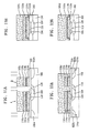
- FIGS. 1 and 2 are cross-sectional views of conventional EEPROM devices.
- FIG. 3 is a plan view of EEPROM devices according to the present invention.
- FIGS. 4A and 4B are cross-sectional views of EEPROM devices of FIG. 3, taken along lines 4 A- 4 A′ and 4 B- 4 B′ of FIG. 3 .
- FIGS. 5A-12A are cross-sectional views of integrated circuit devices according to the present invention taken along the line 4 A- 4 A′ in FIG. 3, during intermediate fabrication steps.
- FIGS. 5B-12B are cross-sectional views of integrated circuit devices according to the present invention taken along the line 4 B— 4 B′ in FIG. 3, during intermediate fabrication steps.
- an EEPROM unit cell can include only one sense transistor gate and only one select transistor gate.
- the sense transistor gate includes a floating gate, an interlevel insulating layer and a sense gate.
- the select transistor gate includes a first select gate, an interlevel insulating layer and a second select gate.
- the gates may be formed using one photolithography process. Accordingly, the unit cell size of EEPROMs may be reduced and/or the reliability of the fabrication process may be enhanced.
- an integrated circuit substrate 100 such as a monocrystalline silicon substrate, may include a field isolation layer such as a field oxide layer 102 that defines active regions of the integrated circuit substrate.
- a thin tunnel insulating layer 110 for example having thickness of between about 50 ⁇ and about 90 ⁇ , and a thick gate insulating layer 104 , for example having a thickness of between about 300 ⁇ and about 500 ⁇ , are included on the active portions of the integrated circuit substrate 100 between the field insulation regions 102 .
- a sense transistor gate I is provided on the tunnel insulating layer 110 and on the gate insulating layer 104 .
- the sense transistor gate comprises a floating gate 112 a on the tunnel insulating layer 110 and on the gate insulating layer 104 , a first interlevel insulating layer 114 a on the floating gate 112 a and a sense gate 116 a on the first interlevel insulating layer 114 a opposite the floating gate 112 a .
- the select transistor gate II is provided on the gate insulating layer 104 and spaced apart from the sense transistor gate I.
- the select transistor gate comprises a first select gate 112 b , on the gate insulating layer 104 that is spaced apart from the sense transistor gate 112 a , a second interlevel insulating layer 114 b on the first select gate 112 b opposite the gate insulating layer 104 , and a second select gate 116 b on the second interlevel insulating layer 114 b opposite the first select gate 112 b , that is spaced apart from the sense gate 116 a .
- the first and second select gates 112 b and 116 b may be electrically connected by a buried contact or other conventional means.
- a first doped region comprising a first portion 108 and a second portion 118 is included in the integrated circuit substrate 100 beneath the tunnel insulating layer 110 and extending to beneath the select transistor gate II. More particularly, the first portion 108 of the first doped region extends from beneath the tunnel insulating layer 110 to outside the sense transistor gate I and the second portion 118 extends from the first portion 108 to beneath the select transistor gate II.
- a second doped region also referred to as a source region, also is included in the integrated circuit substrate beneath the sense transistor gate I and spaced apart from the first doped region 108 / 118 .
- the second doped region preferably comprises a first portion 120 b that is outside the sense transistor gate I and a second portion 120 a that extends from the first portion 120 b to beneath the sense transistor gate I.
- a third doped region also referred to as a drain region, also is provided in the integrated circuit substrate beneath the select transistor gate II and spaced apart from the first doped region 108 / 118 .
- the third doped region preferably comprises a first portion 122 b that is outside the select transistor gate II and a second portion 122 a that extends from the first portion 122 b to beneath the select transistor gate II.
- the second portions thereof preferably are lightly doped relative to the first portions thereof.
- the first, second and third doped regions also preferably form junctions with the integrated circuit substrate 100 .
- the floating gate 112 a and the first select gate 112 b preferably comprise respective first and second portions of a first layer, and the sense gate 116 a and the second select gate 116 b preferably comprise first and second portions of the second layer.
- the first and second layers preferably comprise polysilicon and may include polycide, such as polysilicon and tungsten silicide.
- the first and second interlevel insulating layers 114 a and 114 b also preferably are first and second portions of a third layer.
- the third layer preferably comprises oxide and can include silicon oxynitride.
- reference T designates the active region on the substrate 100 .
- Reference S designates the portion where only the interlevel insulating layer 114 and the sense gate 116 a are formed on the field insulating layer 102 without the floating gate 112 .
- Reference C denotes the bit line contact.
- a high voltage such as about 15-18V is applied to the sense gate 116 a .
- a high voltage such as about 15-18V is applied to the second select transistor gate 116 b , which turns on the select transistor, to thereby supply a strong electric field between the first sense gate 116 a of the sense transistor and the bit line.
- the sense gate 116 a is grounded and a high voltage such as about 15-18V is applied to the bit line connected to the drain region 122 a / 122 b , and a high voltage such as about 15-18V is applied to the second select gate 116 b which selectively turns on the select transistor.
- a strong electric field is applied to both ends of the tunnel insulating layer 110 beneath the floating gate 112 a and the substrate 100 , electrons stored in the floating gate 112 a penetrate the thin barrier and are discharged toward the drain region 122 a / 122 b in the substrate 100 through the first doped region 108 / 118 .
- data programming is performed.
- Vpp represents a high voltage, such as about 15-18V
- GND represents ground potential
- FIGS. 5A-12A and 5 B- 12 B illustrate EEPROM devices according to the present invention during intermediate fabrication steps.
- a field oxide region 102 is formed in an integrated circuit substrate 100 , to define an active region and an inactive region.
- Conventional field isolation such as thermal oxidation and/or trench isolation may be used.
- a gate insulating layer 104 is formed on the active region of the substrate 100 between the field isolation regions 102 .
- the gate insulating layer may have a thickness of between 300 ⁇ and about 500 ⁇ .
- a first photoresist pattern 106 a is formed and dopants are implanted into a first portion of the integrated circuit substrate through the gate insulating layer 104 to form the first doped region 108 .
- a heavily doped implant of ions of conductivity opposite the substrate for example n+-type ions, preferably are implanted into the exposed part of the gate insulating layer 104 .
- the first photoresist pattern 106 a is removed and a second photoresist pattern 106 b is formed, to expose a portion of the first doped region 108 .
- the gate insulating layer 104 is removed from on the portion of the first doped region 108 , to thereby expose the portion of the first doped region. Wet etching may be used.
- the tunnel insulating layer 110 may have thickness of between about 50 ⁇ and about 90 ⁇ .
- a first conductive layer 112 preferably comprising polysilicon is blanket formed on the integrated circuit substrate.
- the first conductive layer 112 preferably is patterned to remove a portion thereof from the field isolation regions. This portion is denoted by S in FIGS. 3 and 4B.
- an interlevel insulating layer 114 and a second conductive layer 116 preferably comprising polysilicon are formed on the first conductive layer 112 , including on the field oxide layer.
- the interlevel insulating layer 114 may include a single layer, preferably comprising silicon dioxide or a multilayer structure, for example an oxide/nitride/oxide structure. Other structures also may be used.
- the second conductive layer 116 and/or the first conductive layer 112 may include a polycide structure.
- a third photoresist pattern 106 c is formed on the second conductive layer.
- the second conductive layer 116 , the interlevel insulating layer 114 and the first conductive layer 112 are then patterned, to thereby define the sense transistor gate I and the select transistor gate II.
- the second conductive layer 116 , the interlevel insulating layer 114 and the first conductive layer 112 are successively etched using the photoresist pattern 106 c as a mask.
- the sense transistor gate I including the floating gate 112 a , the first interlevel insulating layer 114 a and the sense gate 116 is formed on the tunnel insulating layer 110 and on the gate insulating layer 104
- the select transistor gate II including the first select gate 112 b , the second interlevel insulating layer 114 b and the second select gate 116 b is formed on the gate insulating layer 104 and spaced apart from the sense transistor gate I.
- ions such as n-type ions of opposite conductivity type to the substrate, are implanted, to thereby form second, third and fourth doped regions 120 a , 122 a and 118 .
- the second and third doped regions 120 a and 122 a form parts of the source region and drain region respectively.
- the third photoresist pattern 106 is removed and a fourth photoresist pattern 106 d is formed.
- heavily doped impurity ions for example n+-type of opposite conductivity type to the substrate are implanted to form fifth doped region 120 b and sixth doped region 122 b within the second and third doped regions 120 a and 122 a respectively.
- the source and drain regions may include lightly doped and heavily doped portions.
- the fourth photoresist pattern 106 d then may be removed.
- the heavily doped source and drain regions 120 b and 122 b may be formed in separate steps in FIGS. 12A and 12B, by removing the third photoresist pattern 106 c , forming the heavily doped source region 120 a by implanting heavily doped ions into the substrate, forming an insulating layer, selectively etching the insulating layer to define a bit line and implanting heavily doped ions to form the heavily doped drain region 122 b .
- Many other variations in the structures and processes described above may be provided.
- the sense transistor gate I and the select transistor gate II both may have multilayered structures, and may be formed at the same time in a single etch step, using the third photoresist pattern 106 c as a mask. Accordingly, alignment between the floating gate 112 a and the sense gate 116 a may be improved. Moreover, since only one floating gate 112 a and one sense gate 116 a is formed, the unit cell size of the EEPROM may be reduced.
Abstract
EEPROM devices may be fabricated by forming a gate insulating layer and a tunnel insulating layer that is thinner than the gate insulating layer on an integrated circuit substrate, and a first doped region in the integrated circuit substrate beneath the tunnel insulating layer and beneath a portion of the gate insulating layer. A first conductive layer, an interlevel insulating layer and a second conductive layer are sequentially formed on the tunnel insulating layer and on the gate insulating layer. The second conductive layer, the interlevel insulating layer and the first conductive layer then are patterned, to define a sense transistor gate on the tunnel insulating layer and on the gate insulating layer that comprises a first portion of the first conductive layer, a first portion of the interlevel insulating layer and a first portion of the second conductive layer, and to further define a select transistor gate on the gate insulating layer and spaced apart from the sense transistor gate, that comprises a second portion of the first conductive layer, a second portion of the interlevel insulating layer, and a second portion of the second conductive layer.
Description
This application is a divisional application of U.S. patent application Ser. No. 09/426,734, filed on Oct. 26, 1999 now U.S. Pat No. 6,483,145, and claims the benefit of Korean Patent Application No. 1998-57517, filed Dec. 23, 1998, the disclosures of which are hereby incorporated herein by reference as if set forth in their entirety.
This invention relates to integrated circuit memory devices and fabrication methods therefor, and more particularly to EEPROM memory devices and methods of fabricating the same.
EEPROMs are nonvolatile memory devices that are electrically programmable. For electrical reprogrammability, an EEPROM can use a mechanism known as Fowler-Nordheim tunneling, also referred to as electron tunneling, or simply tunneling. Fowler-Nordheim tunneling is a quantum mechanical effect which allows electrons to pass through an energy barrier at a silicon-silicon dioxide interface at a lower energy than the 3.2 eV that is generally required to pass over this energy barrier.
Flash-type EEPROMs may include a one-transistor storage cell. Other types of EEPROMs may include a two-transistor storage cell. The basic two-transistor storage cell includes an access or select transistor and a double polysilicon storage or sense transistor. The sense transistor includes a floating polysilicon gate that is isolated in silicon dioxide, and that is capacitively coupled to a second polysilicon control gate that is stacked above it. The floating gate tunneling oxide cell is often referred to as a FLoating gate Tunnel OXide or FLOTOX-type of EEPROM. An overview of EEPROMs is provided in Chapter 12 of the textbook entitled Semiconductor Memories, pp. 609-650, the disclosure of which is hereby incorporated herein by reference.
FIG. 1 is a cross-sectional view of a first conventional FLOTOX-type EEPROM memory cell. As shown in FIG. 1, a thin tunnel insulating layer 16 and a thick gate insulating layer 12 are formed on an integrated circuit substrate 10, such as a monocrystalline silicon substrate. A sense transistor gate I is a multilayered structure including a floating gate 18, an interlevel insulating layer 20 and a sense gate 22 on the tunnel insulating layer 16 and on a portion of the gate insulating layer 12. A select transistor gate II includes a single select gate layer 24 on the gate insulating layer 12 and spaced apart from the sense transistor gate I.
Continuing with the description of FIG. 1, a doped region 14 extends from beneath the tunnel insulating layer 16 to beneath the select transistor gate II. A second doped region, also referred to as a source region 26, is spaced apart from the first doped region 14 and extends from beneath the sense gate I to outside the sense gate. Finally, a third doped region 28 is spaced apart from the first and second doped regions 14 and 26, and extends from beneath the select gate II to outside the select gate II. Each of the first, second and third doped regions 14, 26 and 28 preferably forms a semiconductor junction with the substrate 10.
The floating gate 18 may be fabricated from a first polysilicon layer and the sense gate 22 and the select gate layer 24 may be fabricated from a second polysilicon layer. As also shown in FIG. 1, the sense gate 22 may be narrower than the floating gate 18. EEPROM cells according to FIG. 1 may be fabricated by patterning a first polysilicon layer to fabricate the floating gate 18. Then, the sense gate 22 and the single select gate layer 24 may be patterned from a second polysilicon layer in a second photolithography process. Unfortunately, in such a process, it may be difficult to align the sense gate 22 to the floating gate 18 when the size of the memory cell is decreased. Moreover, short circuits may be produced by residual polysilicon material that is generated when etching the second polysilicon layer, which can reduce process reliability.
FIG. 2 is a cross-sectional view of another conventional EEPROM storage cell. In the device of FIG. 2, the floating gate 58 a and the sense gates 62 a that form the sense transistor gate I are separated into two spaced apart portions. Moreover, the select transistor gate II may be formed from two layers of polysilicon 58 b and 62 b that are separated by an interlevel insulating layer 60, and that may be electrically interconnected, for example using a suitable buried contact or other means well known to those having skill in the art. The sense transistor gate I and the select transistor gate II may be formed in a one step etching process by etching a second polysilicon layer 62, an interlevel insulating layer 60 and a first polysilicon layer 58 in sequence. A first doped region 54 is formed beneath the tunnel insulating layer 56 and beneath the gate insulating layer 52 in the integrated circuit substrate 50. Second and third (source and drain) doped regions 64 and 66 also may be formed. See U.S. Pat. No. 4,477,825 to Yaron et al.
In the EEPROM cell of FIG. 2, alignment of the sense gate 62 a to the floating gate 58 a may be improved, since a single photolithography step may be used. However, since the floating gates 58 a and the sense gates 62 a are separated, the unit cell size may be larger than the device of FIG. 1. Accordingly, it may be difficult to form highly integrated EEPROM devices using the unit cell of FIG. 2.
It is therefore an object of the present invention to provide improved EEPROM devices and methods of fabricating the same.
It is another object of the present invention to provide EEPROM devices and fabrication methods that can provide improved alignment between the floating gate and the sense gate thereof.
It is still another object of the present invention to provide EEPROM devices and fabrication methods that can be highly integrated with high reliability.
These and other objects can be provided, according to the present invention, by EEPROM devices that include a gate insulating layer and a tunnel insulating layer that is thinner than the gate insulating layer, on an integrated circuit substrate, and a sense transistor gate on the tunnel insulating layer and on the gate insulating layer. The sense transistor gate comprises a floating gate on the tunnel insulating layer and on the gate insulating layer, a first interlevel insulating layer on the floating gate opposite the tunnel insulating layer and the gate insulating layer, and a sense gate on the first interlevel insulating layer opposite the floating gate. A select transistor gate also is included on the gate insulating layer and spaced apart from the sense transistor gate. The select transistor gate comprises a first select gate on the gate insulating layer that is spaced apart from the sense transistor gate, a second interlevel insulating layer on the first select gate opposite the gate insulating layer, and a second select gate on the second interlevel insulating layer opposite the first select gate that is spaced apart from the sense gate.
EEPROM devices according to the present invention also include first, second and third doped regions in the integrated circuit substrate. The first doped region is beneath the tunnel insulating layer and extends to beneath the select transistor gate. The second doped region is beneath the sense transistor gate and is spaced apart from the first doped region. The third doped region is beneath the select transistor gate and is spaced apart from the first doped region.
The floating gate and the first select gate preferably comprise respective first and second portions of a first layer, and the sense gate and the second select gate preferably comprise respective first and second portions of a second layer. The first and second layers preferably comprise polysilicon and may comprise polycide. The first and second interlevel insulating layer also preferably are first and second portions of a third layer that preferably comprises oxide such as silicon dioxide and/or silicon oxynitride.
The first, second and third doped regions also may include lightly doped and heavily doped portions. In particular, the first doped region may comprise a first portion that extends from beneath the tunnel insulating layer to outside the sense transistor gate, and a second portion that extends from the first portion to beneath the select transistor gate. The second doped region may comprise a first portion that is outside the sense transistor gate and a second portion that extends from the first portion to beneath the sense transistor gate. The third doped region may comprise a first portion that is outside the select transistor gate, and a second portion that extends from the first portion to beneath the select transistor gate. In each of these regions, the second portion preferably is lightly doped relative to the first portion. Accordingly, since only one floating gate is used in the unit cell, highly integrated unit cells may be provided.
EEPROM devices may be fabricated, according to the present invention, by forming a gate insulating layer and a tunnel insulating layer that is thinner than the gate insulating layer on an integrated circuit substrate, and a first doped region in the integrated circuit substrate beneath the tunnel insulating layer and beneath a portion of the gate insulating layer. A first conductive layer, an interlevel insulating layer and a second conductive layer are sequentially formed on the tunnel insulating layer and on the gate insulating layer. The second conductive layer, the interlevel insulating layer and the first conductive layer then are patterned, to define a sense transistor gate on the tunnel insulating layer and on the gate insulating layer that comprises a first portion of the first conductive layer, a first portion of the interlevel insulating layer and a first portion of the second conductive layer, and to further define a select transistor gate on the gate insulating layer and spaced apart from the sense transistor gate, that comprises a second portion of the first conductive layer, a second portion of the interlevel insulating layer, and a second portion of the second conductive layer.
Then, second, third and fourth doped regions are simultaneously formed in the integrated circuit substrate using the sense transistor gate and the select transistor gate as a mask. The second, third and fourth doped regions are spaced apart from each other. The second doped region extends from beneath the sense transistor gate to outside the sense transistor gate. The third doped region extends from beneath the select transistor gate to outside the select transistor gate. The doped region extends from the first doped region to beneath the select transistor gate.
Thereafter, a fifth doped region may be formed within the second doped region outside the sense transistor gate and a sixth doped region may be formed within the third doped region outside the select transistor gate. The fifth and sixth doped regions may be formed simultaneously. The first, fifth and sixth doped regions preferably are heavily doped relative to the respective fourth, second and third doped regions.
The gate insulating layer, tunnel insulating layer and first doped region preferably are formed by forming the gate insulating layer on the integrated circuit substrate and implanting dopants into a first portion of the integrated circuit substrate through the gate insulating layer to form the first doped region. The gate insulating layer then is removed from a portion of the first doped region, to expose the portion of the first doped region. The tunnel insulating layer then is formed on the exposed portion of the first doped region.
The integrated circuit substrate also may include field isolation regions therein. In this case, the first conductive layer may be blanket formed on the integrated circuit substrate including on the field isolation regions, and then patterned to remove a portion thereof from the field isolation regions. The interlevel insulating layer and the second conductive layer then may be blanket formed. Since the sense transistor gate and select transistor gate may be simultaneously defined, alignment between the floating gate and the sense gate may be improved. Accordingly, highly integrated and/or highly reliable EEPROMs may be fabricated.
FIGS. 1 and 2 are cross-sectional views of conventional EEPROM devices.
FIG. 3 is a plan view of EEPROM devices according to the present invention.
FIGS. 4A and 4B are cross-sectional views of EEPROM devices of FIG. 3, taken along lines 4A-4A′ and 4B-4B′ of FIG. 3.
FIGS. 5A-12A are cross-sectional views of integrated circuit devices according to the present invention taken along the line 4A-4A′ in FIG. 3, during intermediate fabrication steps.
FIGS. 5B-12B are cross-sectional views of integrated circuit devices according to the present invention taken along the line 4B—4B′ in FIG. 3, during intermediate fabrication steps.
The present invention now will be described more fully hereinafter with reference to the accompanying drawings, in which preferred embodiments of the invention are shown. This invention may, however, be embodied in many different forms and should not be construed as limited to the embodiments set forth herein; rather, these embodiments are provided so that this disclosure will be thorough and complete, and will fully convey the scope of the invention to those skilled in the art. In the drawings, the thickness of layers and regions are exaggerated for clarity. Like numbers refer to like elements throughout. It will be understood that when an element such as a layer, region or substrate is referred to as being “on” another element, it can be directly on the other element or intervening elements may also be present. In contrast, when an element is referred to as being “directly on” another element, there are no intervening elements present. Moreover, each embodiment described and illustrated herein includes its complementary conductivity type embodiment as well.
According to the invention, an EEPROM unit cell can include only one sense transistor gate and only one select transistor gate. The sense transistor gate includes a floating gate, an interlevel insulating layer and a sense gate. The select transistor gate includes a first select gate, an interlevel insulating layer and a second select gate. The gates may be formed using one photolithography process. Accordingly, the unit cell size of EEPROMs may be reduced and/or the reliability of the fabrication process may be enhanced.
Referring now of FIGS. 3, 4A and 4B, an integrated circuit substrate 100, such as a monocrystalline silicon substrate, may include a field isolation layer such as a field oxide layer 102 that defines active regions of the integrated circuit substrate. A thin tunnel insulating layer 110, for example having thickness of between about 50 Å and about 90 Å, and a thick gate insulating layer 104, for example having a thickness of between about 300 Å and about 500 Å, are included on the active portions of the integrated circuit substrate 100 between the field insulation regions 102. A sense transistor gate I is provided on the tunnel insulating layer 110 and on the gate insulating layer 104. The sense transistor gate comprises a floating gate 112 a on the tunnel insulating layer 110 and on the gate insulating layer 104, a first interlevel insulating layer 114 a on the floating gate 112 a and a sense gate 116 a on the first interlevel insulating layer 114 a opposite the floating gate 112 a. The select transistor gate II is provided on the gate insulating layer 104 and spaced apart from the sense transistor gate I. The select transistor gate comprises a first select gate 112 b, on the gate insulating layer 104 that is spaced apart from the sense transistor gate 112 a, a second interlevel insulating layer 114 b on the first select gate 112 b opposite the gate insulating layer 104, and a second select gate 116 b on the second interlevel insulating layer 114 b opposite the first select gate 112 b, that is spaced apart from the sense gate 116 a. The first and second select gates 112 b and 116 b may be electrically connected by a buried contact or other conventional means.
A first doped region comprising a first portion 108 and a second portion 118 is included in the integrated circuit substrate 100 beneath the tunnel insulating layer 110 and extending to beneath the select transistor gate II. More particularly, the first portion 108 of the first doped region extends from beneath the tunnel insulating layer 110 to outside the sense transistor gate I and the second portion 118 extends from the first portion 108 to beneath the select transistor gate II.
A second doped region, also referred to as a source region, also is included in the integrated circuit substrate beneath the sense transistor gate I and spaced apart from the first doped region 108/118. As shown in FIG. 4A, the second doped region preferably comprises a first portion 120 b that is outside the sense transistor gate I and a second portion 120 a that extends from the first portion 120 b to beneath the sense transistor gate I.
A third doped region, also referred to as a drain region, also is provided in the integrated circuit substrate beneath the select transistor gate II and spaced apart from the first doped region 108/118. The third doped region preferably comprises a first portion 122 b that is outside the select transistor gate II and a second portion 122 a that extends from the first portion 122 b to beneath the select transistor gate II. In the first, second and third doped regions, the second portions thereof preferably are lightly doped relative to the first portions thereof. The first, second and third doped regions also preferably form junctions with the integrated circuit substrate 100.
As will be described below, the floating gate 112 a and the first select gate 112 b preferably comprise respective first and second portions of a first layer, and the sense gate 116 a and the second select gate 116 b preferably comprise first and second portions of the second layer. The first and second layers preferably comprise polysilicon and may include polycide, such as polysilicon and tungsten silicide. The first and second interlevel insulating layers 114 a and 114 b also preferably are first and second portions of a third layer. The third layer preferably comprises oxide and can include silicon oxynitride.
Finally, referring to FIG. 3, reference T designates the active region on the substrate 100. Reference S designates the portion where only the interlevel insulating layer 114 and the sense gate 116 a are formed on the field insulating layer 102 without the floating gate 112. Reference C denotes the bit line contact.
Operations for storing (writing), erasing and reading data in EEPROMs of FIGS. 3 and 4A-4B will be described briefly. In particular, for erasing, a high voltage such as about 15-18V is applied to the sense gate 116 a. When the bit line connected to the drain region 122 a/122 b is grounded, a high voltage such as about 15-18V is applied to the second select transistor gate 116 b, which turns on the select transistor, to thereby supply a strong electric field between the first sense gate 116 a of the sense transistor and the bit line. Some of the electrons supplied from the bit line are injected into the floating gate 112 a and tunnel through the tunnel insulating layer 112, and thereby provide an erasing operation. Thus, if the floating gate 112 a is filled with electrons, the threshold voltage of the memory cell increases. Moreover, a channel is not generated because of the high threshold voltage, so that the off-state is memorized.
In order to store new data, the sense gate 116 a is grounded and a high voltage such as about 15-18V is applied to the bit line connected to the drain region 122 a/122 b, and a high voltage such as about 15-18V is applied to the second select gate 116 b which selectively turns on the select transistor. Thus, if a strong electric field is applied to both ends of the tunnel insulating layer 110 beneath the floating gate 112 a and the substrate 100, electrons stored in the floating gate 112 a penetrate the thin barrier and are discharged toward the drain region 122 a/122 b in the substrate 100 through the first doped region 108/118. As a result, data programming is performed. Thereafter, if the cell is read by applying power to the second select gate 116 b that serves as a word line, current flows through a channel that results from the low threshold. Accordingly, the state can be memorized. Thus, data is read by determining if current is present in the memory cell transistor by applying an appropriate voltage to the bit line and sense gate 116 a of the selected cell. Table 1 summarizes the operational conditions for EEPROM cells according to the present invention.
| TABLE 1 | ||||||
| Source | ||||||
| Bit line | Second select gate | Sense gate | region | Bulk | ||
| Program | Vpp | Vpp | GND | floating | GND |
| Erase | GND | Vpp | Vpp | GND | GND |
| Read | 1-3 V | 1-5 V | 0.5-2 V | GND | GND |
In the Table, Vpp represents a high voltage, such as about 15-18V, and GND represents ground potential.
Methods of fabricating EEPROM devices according to the invention now will be described. FIGS. 5A-12A and 5B-12B illustrate EEPROM devices according to the present invention during intermediate fabrication steps.
Referring now to FIGS. 5A and 5B, a field oxide region 102 is formed in an integrated circuit substrate 100, to define an active region and an inactive region. Conventional field isolation, such as thermal oxidation and/or trench isolation may be used. A gate insulating layer 104 is formed on the active region of the substrate 100 between the field isolation regions 102. The gate insulating layer may have a thickness of between 300 Å and about 500 Å.
Then, referring to FIGS. 6A and 6B, a first photoresist pattern 106 a is formed and dopants are implanted into a first portion of the integrated circuit substrate through the gate insulating layer 104 to form the first doped region 108. It will be understood that a heavily doped implant of ions of conductivity opposite the substrate, for example n+-type ions, preferably are implanted into the exposed part of the gate insulating layer 104.
Referring now to FIGS. 7A and 7B, the first photoresist pattern 106 a is removed and a second photoresist pattern 106 b is formed, to expose a portion of the first doped region 108. The gate insulating layer 104 is removed from on the portion of the first doped region 108, to thereby expose the portion of the first doped region. Wet etching may be used.
Then, referring to FIGS. 8A and 8B, the second photoresist pattern 106 b is removed and the tunnel insulating layer 110 is formed on the exposed portion of the first doped region 108. The tunnel insulating layer 110 may have thickness of between about 50 Å and about 90 Å.
Referring now to FIGS. 9A and 9B, a first conductive layer 112 preferably comprising polysilicon is blanket formed on the integrated circuit substrate. In order to separate the floating gates between unit cells, the first conductive layer 112 preferably is patterned to remove a portion thereof from the field isolation regions. This portion is denoted by S in FIGS. 3 and 4B.
Referring now to FIGS. 10A and 10B, an interlevel insulating layer 114 and a second conductive layer 116 preferably comprising polysilicon are formed on the first conductive layer 112, including on the field oxide layer. It will be understood that the interlevel insulating layer 114 may include a single layer, preferably comprising silicon dioxide or a multilayer structure, for example an oxide/nitride/oxide structure. Other structures also may be used. It also will be understood that the second conductive layer 116 and/or the first conductive layer 112 may include a polycide structure.
Referring now to FIGS. 11A and 11B, a third photoresist pattern 106 c is formed on the second conductive layer. The second conductive layer 116, the interlevel insulating layer 114 and the first conductive layer 112 are then patterned, to thereby define the sense transistor gate I and the select transistor gate II. Preferably, the second conductive layer 116, the interlevel insulating layer 114 and the first conductive layer 112 are successively etched using the photoresist pattern 106 c as a mask. As a result, the sense transistor gate I including the floating gate 112 a, the first interlevel insulating layer 114 a and the sense gate 116 is formed on the tunnel insulating layer 110 and on the gate insulating layer 104, and the select transistor gate II including the first select gate 112 b, the second interlevel insulating layer 114 b and the second select gate 116 b is formed on the gate insulating layer 104 and spaced apart from the sense transistor gate I.
Still referring to FIGS. 11A and 11B, ions, such as n-type ions of opposite conductivity type to the substrate, are implanted, to thereby form second, third and fourth doped regions 120 a, 122 a and 118. The second and third doped regions 120 a and 122 a form parts of the source region and drain region respectively.
Finally, referring to FIGS. 12A and 12B, the third photoresist pattern 106 is removed and a fourth photoresist pattern 106 d is formed. Using the fourth photoresist pattern as a mask, heavily doped impurity ions, for example n+-type of opposite conductivity type to the substrate are implanted to form fifth doped region 120 b and sixth doped region 122 b within the second and third doped regions 120 a and 122 a respectively. Accordingly, the source and drain regions may include lightly doped and heavily doped portions. The fourth photoresist pattern 106 d then may be removed.
It also will be understood that the process sequence described above may be varied. For example, the heavily doped source and drain regions 120 b and 122 b may be formed in separate steps in FIGS. 12A and 12B, by removing the third photoresist pattern 106 c, forming the heavily doped source region 120 a by implanting heavily doped ions into the substrate, forming an insulating layer, selectively etching the insulating layer to define a bit line and implanting heavily doped ions to form the heavily doped drain region 122 b. Many other variations in the structures and processes described above may be provided.
Accordingly, the sense transistor gate I and the select transistor gate II both may have multilayered structures, and may be formed at the same time in a single etch step, using the third photoresist pattern 106 c as a mask. Accordingly, alignment between the floating gate 112 a and the sense gate 116 a may be improved. Moreover, since only one floating gate 112 a and one sense gate 116 a is formed, the unit cell size of the EEPROM may be reduced.
In the drawings and specification, there have been disclosed typical preferred embodiments of the invention and, although specific terms are employed, they are used in a generic and descriptive sense only and not for purposes of limitation, the scope of the invention being set forth in the following claims.
Claims (13)
1. A method of fabricating an electrically erasable programmable read only memory (EEPROM) comprising the steps of:
forming a gate insulating layer and a tunnel insulating layer that is thinner than the gate insulating layer on an integrated circuit substrate, and a first doped region in the integrated circuit substrate beneath the tunnel insulating layer and beneath a portion of the gate insulating layer;
sequentially forming a first conductive layer, an interlevel insulating layer and a second conductive layer on the tunnel insulating layer and on the gate insulating layer;
patterning the second conductive layer, the interlevel insulating layer an the first conductive layer to define a sense transistor gate on the tunnel insulating layer and on the gate insulating layer, the sense transistor gate comprising a first portion of the first conductive layer, a first portion of the interlevel insulating layer and a first portion of the second conductive layer, and to further define a select transistor gate on the gate insulating layer and spaced apart from the sense transistor gate, the select transistor gate comprising a second portion of the first conductive layer, a second portion of the interlevel insulating layer and a second portion of the second conductive layer; and
simultaneously forming second, third and fourth doped regions in the integrated circuit substrate using the sense transistor gate and the select transistor gate as a mask, the second, third and fourth doped regions being spaced apart from each other, the second doped region extending from beneath the sense transistor gate to outside the sense transistor gate, the third doped region extending from beneath the select transistor gate to outside the select transistor gate, and the fourth doped region extending from the first doped region to beneath a select gate electrode of the select transistor gate
simultaneously forming a fifth doped region within the second doped region outside the sense transistor gate and a sixth doped region within the third doped region outside the select transistor gate, using a photoresist pattern as a mask extending from outside the sense transistor gate to outside the select transistor gate.
2. A method according to claim 1 wherein the first, fifth and sixth doped regions are heavily doped relative to the respective fourth, second an third doped regions.
3. A method according to claim 1 wherein the step of forming a gate insulating layer and a tunnel insulating layer on an integrated circuit substrate and a first doped region in the integrated circuit substrate beneath the tunnel insulating layer and beneath a portion of the gate insulating layer, comprises the steps of:
forming the gate insulating layer on the integrated circuit substrate;
implanting dopants into a first portion of the integrated circuit substrate through the gate insulating layer to form the first doped region;
removing the gate insulating layer from a portion of the first doped region to expose the portion of the first doped region; and
forming the tunnel insulating layer on the exposed portion of the first doped region.
4. A method according to claim 1 wherein the integrated circuit substrate also includes field isolation regions therein and wherein the step of sequentially forming a first conductive layer, an interlevel insulating layer and a second conductive layer on the tunnel insulating layer and on the gate insulating layer comprises the steps of:
blanket forming the first conductive layer on the integrated circuit substrate including on the field isolation regions;
patterning the first conductive layer to remove a portion thereof from the field isolation regions;
blanket forming the interlevel insulating layer on the patterned first conductive layer and on the field isolation regions; and
blanket forming the second conductive layer on the interlevel insulating layer.
5. A method according to claim 1 wherein the first and second conducive layers comprise polysilicon.
6. A method according to claim 1 wherein the interlevel insulating layer comprises oxide.
7. A method of fabricating an electrically erasable programmable read only memory (EEPROM) comprising:
forming an integrated circuit substrate;
forming a gate insulating layer and a tunnel insulating layer that is thinner than the gate insulating layer, on the integrated circuit substrate;
forming a sense transistor gate on the tunnel insulating layer and on the gate insulating layer, the sense transistor gate comprising a floating gate on the tunnel insulating layer and on the gate insulating layer, a first interlevel insulating layer on the floating gate opposite the tunnel insulating layer and the gate insulating layer, and a sense gate on the first interlevel insulating layer opposite the floating gate;
forming a select transistor gate on the gate insulating layer and spaced apart from the sense transistor gate, the select transistor gate comprising a first select gate a the gate insulating layer that is spaced apart from the sense transistor gate, a second interlevel insulating layer on the first select gate opposite the gate insulating layer, and a second select gate on the second interlevel insulating layer opposite the first select gate that is spaced apart from the sense gate;
forming a first doped region in the integrated circuit substrate beneath the tunnel insulating layer and extending in the integrated substrate to beneath the select transistor gate, wherein forming the first doped region comprises:
forming a first portion that extends from beneath the tunnel insulating layer to outside the sense transistor gate and extends to a first depth in the integrated circuit substrate; and
forming a second portion that extends from the first portion to beneath a select gate electrode of the select transistor gate, extends to the first depth and is lightly doped relative to the first portion;
forming a second doped region in the integrated circuit substrate beneath the sense transistor gate and spaced apart from the first doped region, wherein forming the second doped region comprises:
forming a third portion outside the sense transistor gate using a photoresist pattern as a mask extending from outside the sense transistor sate to outside the select transistor gate and extending to a second depth in the integrated circuit substrate; and
forming a fourth portion extending from the third portion to beneath the sense transistor gate, extending to a third depth in the integrated circuit substrate, deeper than the second depth, and being lightly doped relative to the third portion; and
forming a third doped region in the integrated circuit substrate beneath the select transistor gate and spaced apart from the first doped region, wherein forming the third doped region comprises:
forming a fifth portion outside the select transistor gate using the photoresist pattern as a mask extending from outside the sense transistor gate to outside the select transistor gate and extending to a fourth depth in the integrated circuit substrate; and
forming a sixth portion extending from the fifth portion to beneath the select transistor gate, extending to a fifth depth in the integrated circuit substrate, deeper than the fourth depth, and being lightly doped relative to the fifth portion.
8. A method according to claim 7 wherein the floating gate and the first select gate comprise respective first and second portions of a first layer and wherein the sense gate and the second select gate comprise respective first and second portions of a second layer.
9. A method according to claim 8 wherein the first and second layers are first and second layers that comprise polysilicon.
10. A method according to claim 8 wherein the first and second interlevel insulating layers are first and second portions of a third layer.
11. A method according to claim 7 , wherein the first, third and fifth depths are equal and wherein the second and fourth depths are equal.
12. A method of forming an electrically erasable programmable read only memory (EEPROM) comprising;
forming an integrated circuit substrate;
forming a gate insulating layer and a tunnel insulating layer that is thinner than the gate insulating layer, on the integrated circuit substrate;
forming a sense transistor gate on the tunnel insulating layer and on the gate insulating layer, the sense transistor gate comprising a floating gate on the tunnel insulating layer and on the gate insulating layer, a first interlevel insulating layer on the floating gate opposite the tunnel insulating layer and the gate insulating layer, and a sense gate on the first interlevel insulating layer opposite the floating gate;
forming a select transistor gate on the gate insulating layer and spaced apart from the sense transistor gate, the select transistor gate comprising a first select gate on the gate insulating layer that is spaced apart from the sense transistor gate, a second interlevel insulating layer on the first select gate opposite the gate insulating layer, and a second select gate on the second interlevel insulating layer opposite the first select gate that is spaced apart from the sense gate;
forming a first doped region in the integrated circuit substrate that extends from beneath the tunnel insulating layer to outside the sense transistor gate and extends to a first depth in the integrated circuit substrate;
forming a second doped region in the integrated circuit substrate that extends from the first doped region to beneath a select gate electrode of the select transistor gate, extends to the first depth and is lightly doped relative to the first doped region;
forming a third doped region in the integrated circuit substrate that is outside the sense transistor gate using a photoresist pattern as a mask extending from outside the sense transistor gate to outside the select transistor gate and extends to a second depth in the integrated circuit substrate;
forming a fourth doped region in the integrated circuit substrate that extends from the third doped region to beneath the sense transistor gate, extends to a third depth in the integrated circuit substrate, deeper then the second depth, and is lightly doped relative to the third doped region;
forming a fifth doped region in the integrated circuit substrate that is outside the select transistor gate using the photoresist pattern as a mask extending from outside the sense transistor gate to outside the select transistor gate and extends to a fourth depth in the integrated circuit substrate; and
forming a sixth doped region that extends from the fifth doped region to beneath the select transistor gate, extending to a fifth depth in the integrated circuit substrate, deeper than the fourth depth, and is lightly doped relative to the fifth doped region.
13. A method according to claim 12 , wherein the first, third and fifth depths are equal and wherein the second and fourth depths are equal.
Priority Applications (2)
| Application Number | Priority Date | Filing Date | Title |
|---|---|---|---|
| US10/259,090 US6818509B2 (en) | 1998-12-23 | 2002-09-27 | Methods of fabricating electrically erasable programmable read-only memory (EEPROM) devices including multilayer sense and select transistor gates |
| US10/319,972 US20030089944A1 (en) | 1998-12-23 | 2002-12-16 | Electrically erasable programmable read-only memory (EEPROM) devices including multilayer sense and select transistor gates |
Applications Claiming Priority (4)
| Application Number | Priority Date | Filing Date | Title |
|---|---|---|---|
| KR98-57517 | 1998-12-23 | ||
| KR1019980057517A KR100311971B1 (en) | 1998-12-23 | 1998-12-23 | Non-volatile Memory Semiconductor Device Manufacturing Method |
| US09/426,734 US6483145B1 (en) | 1998-12-23 | 1999-10-26 | Electrically erasable programmable read-only memory (EEPROM) devices including multilayer sense and select transistor gates |
| US10/259,090 US6818509B2 (en) | 1998-12-23 | 2002-09-27 | Methods of fabricating electrically erasable programmable read-only memory (EEPROM) devices including multilayer sense and select transistor gates |
Related Parent Applications (1)
| Application Number | Title | Priority Date | Filing Date |
|---|---|---|---|
| US09/426,734 Division US6483145B1 (en) | 1998-12-23 | 1999-10-26 | Electrically erasable programmable read-only memory (EEPROM) devices including multilayer sense and select transistor gates |
Related Child Applications (1)
| Application Number | Title | Priority Date | Filing Date |
|---|---|---|---|
| US10/319,972 Division US20030089944A1 (en) | 1998-12-23 | 2002-12-16 | Electrically erasable programmable read-only memory (EEPROM) devices including multilayer sense and select transistor gates |
Publications (2)
| Publication Number | Publication Date |
|---|---|
| US20030022447A1 US20030022447A1 (en) | 2003-01-30 |
| US6818509B2 true US6818509B2 (en) | 2004-11-16 |
Family
ID=19564826
Family Applications (2)
| Application Number | Title | Priority Date | Filing Date |
|---|---|---|---|
| US09/426,734 Expired - Fee Related US6483145B1 (en) | 1998-12-23 | 1999-10-26 | Electrically erasable programmable read-only memory (EEPROM) devices including multilayer sense and select transistor gates |
| US10/259,090 Expired - Fee Related US6818509B2 (en) | 1998-12-23 | 2002-09-27 | Methods of fabricating electrically erasable programmable read-only memory (EEPROM) devices including multilayer sense and select transistor gates |
Family Applications Before (1)
| Application Number | Title | Priority Date | Filing Date |
|---|---|---|---|
| US09/426,734 Expired - Fee Related US6483145B1 (en) | 1998-12-23 | 1999-10-26 | Electrically erasable programmable read-only memory (EEPROM) devices including multilayer sense and select transistor gates |
Country Status (3)
| Country | Link |
|---|---|
| US (2) | US6483145B1 (en) |
| KR (1) | KR100311971B1 (en) |
| DE (1) | DE19951930C2 (en) |
Cited By (5)
| Publication number | Priority date | Publication date | Assignee | Title |
|---|---|---|---|---|
| US20040036094A1 (en) * | 2001-05-31 | 2004-02-26 | Semiconductor Energy Laboratory Co., Ltd. | Semiconductor device and an electonic device |
| US20070145472A1 (en) * | 2005-12-26 | 2007-06-28 | Kwak Cheol S | Flash memory cell including dual tunnel oxide layer and method of manufacturing the same |
| US20080313791A1 (en) * | 2005-11-23 | 2008-12-25 | Nagely Scott W | Protective helmet with cervical spine protection and additional brain protection |
| US20100240181A1 (en) * | 2003-05-12 | 2010-09-23 | United Microelectronics Corp. | Method for Forming Single-Level Electrically Erasable and Programmable Read Only Memory Operated in Environment with High/Low-Voltage |
| US20170018622A1 (en) * | 2015-07-17 | 2017-01-19 | Broadcom Corporation | UTBB FDSOI Split Gate Devices |
Families Citing this family (12)
| Publication number | Priority date | Publication date | Assignee | Title |
|---|---|---|---|---|
| TW523881B (en) * | 2001-02-08 | 2003-03-11 | Samsung Electronics Co Ltd | Non-volatile memory device and method of manufacturing the same |
| KR100399415B1 (en) * | 2001-02-08 | 2003-09-26 | 삼성전자주식회사 | Nonvolatile Memory Device and Method of fabricationg the Same |
| US7256449B2 (en) | 2003-05-20 | 2007-08-14 | Samsung Electronics, Co., Ltd. | EEPROM device for increasing a coupling ratio and fabrication method thereof |
| KR100604850B1 (en) * | 2003-05-20 | 2006-07-31 | 삼성전자주식회사 | EEPROM cell structures having non-uniform channel dielectric thickness and methods of making the same |
| JP2005183763A (en) * | 2003-12-22 | 2005-07-07 | Toshiba Microelectronics Corp | Method of manufacturing semiconductor device including non-volatile memory |
| KR100572327B1 (en) * | 2004-07-06 | 2006-04-18 | 삼성전자주식회사 | Method for forming a tunneling insulating layer in a nonvolatible memory device |
| KR100577225B1 (en) * | 2004-12-29 | 2006-05-26 | 동부일렉트로닉스 주식회사 | Electrically erasable programmable rom, method for fabricating the same and method for programming/erasing the same |
| US7488657B2 (en) * | 2005-06-17 | 2009-02-10 | Spansion Llc | Method and system for forming straight word lines in a flash memory array |
| US8236518B2 (en) * | 2005-07-15 | 2012-08-07 | The University Of Vermont And State Agriculture College | Highly sensitive immunoassays and antibodies for detection of blood factor VIII |
| US20070018230A1 (en) * | 2005-07-22 | 2007-01-25 | Samsung Electronics Co.,Ltd. | Eeprom and methods of fabricating the same |
| KR100885779B1 (en) * | 2006-12-28 | 2009-02-26 | 주식회사 하이닉스반도체 | High voltage transistor in flash memory device |
| US9285352B2 (en) * | 2010-12-22 | 2016-03-15 | Drinksavvy, Inc. | System and method for detection of a contaminated beverage |
Citations (8)
| Publication number | Priority date | Publication date | Assignee | Title |
|---|---|---|---|---|
| US3745647A (en) * | 1970-10-07 | 1973-07-17 | Rca Corp | Fabrication of semiconductor devices |
| US4477825A (en) | 1981-12-28 | 1984-10-16 | National Semiconductor Corporation | Electrically programmable and erasable memory cell |
| US5464785A (en) * | 1994-11-30 | 1995-11-07 | United Microelectronics Corporation | Method of making a flash EPROM device having a drain edge P+ implant |
| US5773347A (en) * | 1994-03-25 | 1998-06-30 | Mitsubishi Denki Kabushiki Kaisha | Method of maufacturing field effect transistor |
| US5981342A (en) * | 1996-05-17 | 1999-11-09 | Siemens Aktiengesellschaft | Method of making a semiconductor component with compensation implantation |
| US5981340A (en) | 1997-09-29 | 1999-11-09 | Motorola, Inc. | Method of building an EPROM cell without drain disturb and reduced select gate resistance |
| US6194270B1 (en) * | 1997-08-07 | 2001-02-27 | Stmicroelectronics, S.R.L. | Process for the manufacturing of an electrically programmable non-volatile memory device |
| US6420222B1 (en) * | 1997-03-27 | 2002-07-16 | Seiko Instruments Inc. | Method of producing semiconductor having two-layer polycrystalline silicon structure |
Family Cites Families (4)
| Publication number | Priority date | Publication date | Assignee | Title |
|---|---|---|---|---|
| US5066992A (en) * | 1989-06-23 | 1991-11-19 | Atmel Corporation | Programmable and erasable MOS memory device |
| JPH081933B2 (en) * | 1989-12-11 | 1996-01-10 | 株式会社東芝 | Nonvolatile semiconductor memory device |
| JPH03283569A (en) * | 1990-03-30 | 1991-12-13 | Fujitsu Ltd | Semiconductor device |
| US5550072A (en) * | 1994-08-30 | 1996-08-27 | National Semiconductor Corporation | Method of fabrication of integrated circuit chip containing EEPROM and capacitor |
-
1998
- 1998-12-23 KR KR1019980057517A patent/KR100311971B1/en not_active IP Right Cessation
-
1999
- 1999-10-26 US US09/426,734 patent/US6483145B1/en not_active Expired - Fee Related
- 1999-10-28 DE DE19951930A patent/DE19951930C2/en not_active Expired - Fee Related
-
2002
- 2002-09-27 US US10/259,090 patent/US6818509B2/en not_active Expired - Fee Related
Patent Citations (8)
| Publication number | Priority date | Publication date | Assignee | Title |
|---|---|---|---|---|
| US3745647A (en) * | 1970-10-07 | 1973-07-17 | Rca Corp | Fabrication of semiconductor devices |
| US4477825A (en) | 1981-12-28 | 1984-10-16 | National Semiconductor Corporation | Electrically programmable and erasable memory cell |
| US5773347A (en) * | 1994-03-25 | 1998-06-30 | Mitsubishi Denki Kabushiki Kaisha | Method of maufacturing field effect transistor |
| US5464785A (en) * | 1994-11-30 | 1995-11-07 | United Microelectronics Corporation | Method of making a flash EPROM device having a drain edge P+ implant |
| US5981342A (en) * | 1996-05-17 | 1999-11-09 | Siemens Aktiengesellschaft | Method of making a semiconductor component with compensation implantation |
| US6420222B1 (en) * | 1997-03-27 | 2002-07-16 | Seiko Instruments Inc. | Method of producing semiconductor having two-layer polycrystalline silicon structure |
| US6194270B1 (en) * | 1997-08-07 | 2001-02-27 | Stmicroelectronics, S.R.L. | Process for the manufacturing of an electrically programmable non-volatile memory device |
| US5981340A (en) | 1997-09-29 | 1999-11-09 | Motorola, Inc. | Method of building an EPROM cell without drain disturb and reduced select gate resistance |
Non-Patent Citations (2)
| Title |
|---|
| Betty Prince, Semiconductor Memories: A Handbook of Design, Manufacture and Application, Second Edition, Chapter 12, 1991, pp. 609-650. |
| Woif, "Silicon Processing for the VLSI Era vol. 2: Process Integration", pp. 354-359, 1990, Lattice Press.* * |
Cited By (12)
| Publication number | Priority date | Publication date | Assignee | Title |
|---|---|---|---|---|
| US20040036094A1 (en) * | 2001-05-31 | 2004-02-26 | Semiconductor Energy Laboratory Co., Ltd. | Semiconductor device and an electonic device |
| US7268387B2 (en) * | 2001-05-31 | 2007-09-11 | Semiconductor Energy Laboratory Co., Ltd. | Semiconductor device and an electronic device |
| US20100240181A1 (en) * | 2003-05-12 | 2010-09-23 | United Microelectronics Corp. | Method for Forming Single-Level Electrically Erasable and Programmable Read Only Memory Operated in Environment with High/Low-Voltage |
| USRE44156E1 (en) * | 2003-05-12 | 2013-04-16 | United Microelectronics Corp. | Method for forming single-level electrically erasable and programmable read only memory operated in environment with high/low-voltage |
| US20080313791A1 (en) * | 2005-11-23 | 2008-12-25 | Nagely Scott W | Protective helmet with cervical spine protection and additional brain protection |
| US20110185481A1 (en) * | 2005-11-23 | 2011-08-04 | Scott W. Nagely | Protective helmet with cervical spine protection and additional brain protection |
| US8181281B2 (en) * | 2005-11-23 | 2012-05-22 | Scott W. Nagely | Protective helmet with cervical spine protection and additional brain protection |
| US20120222197A1 (en) * | 2005-11-23 | 2012-09-06 | Scott W. Nagely | Protective helmet with cervical spine protection and additional brain protection |
| US8561217B2 (en) * | 2005-11-23 | 2013-10-22 | Scott W. Nagely | Protective helmet with cervical spine protection and additional brain protection |
| US20070145472A1 (en) * | 2005-12-26 | 2007-06-28 | Kwak Cheol S | Flash memory cell including dual tunnel oxide layer and method of manufacturing the same |
| US20170018622A1 (en) * | 2015-07-17 | 2017-01-19 | Broadcom Corporation | UTBB FDSOI Split Gate Devices |
| US9978848B2 (en) * | 2015-07-17 | 2018-05-22 | Avago Technologies General Ip (Singapore) Pte. Ltd. | UTBB FDSOI split gate devices |
Also Published As
| Publication number | Publication date |
|---|---|
| DE19951930C2 (en) | 2002-07-11 |
| KR100311971B1 (en) | 2001-12-28 |
| US20030022447A1 (en) | 2003-01-30 |
| US6483145B1 (en) | 2002-11-19 |
| DE19951930A1 (en) | 2000-07-06 |
| KR20000041584A (en) | 2000-07-15 |
Similar Documents
| Publication | Publication Date | Title |
|---|---|---|
| US5326999A (en) | Non-volatile semiconductor memory device and manufacturing method thereof | |
| US7015098B2 (en) | Methods and structure for an improved floating gate memory cell | |
| US7816723B2 (en) | Semiconductor memory array of floating gate memory cells with program/erase and select gates | |
| US5646060A (en) | Method for making an EEPROM cell with isolation transistor | |
| KR100217532B1 (en) | Packing density for flash memories | |
| US7205198B2 (en) | Method of making a bi-directional read/program non-volatile floating gate memory cell | |
| US6184093B1 (en) | Method of implementing differential gate oxide thickness for flash EEPROM | |
| JP3733595B2 (en) | Manufacturing method of semiconductor device including MOS element | |
| US6157575A (en) | Nonvolatile memory device and operating method thereof | |
| US6818509B2 (en) | Methods of fabricating electrically erasable programmable read-only memory (EEPROM) devices including multilayer sense and select transistor gates | |
| US6310374B1 (en) | Nonvolatile semiconductor memory device having extracting electrode | |
| US7151021B2 (en) | Bi-directional read/program non-volatile floating gate memory cell and array thereof, and method of formation | |
| KR20010074775A (en) | A single polysilicon flash eeprom and method for making same | |
| JP3397903B2 (en) | Manufacturing method of nonvolatile semiconductor memory device | |
| US20040195614A1 (en) | A non-volatile floating gate memory cell with floating gates formed in cavities, and array thereof, and method of formation | |
| US20070045673A1 (en) | Nonvolatile memory devices and methods of fabricating the same | |
| US6376295B1 (en) | Method for manufacturing a semiconductor memory device with a fine structure | |
| US6680507B2 (en) | Dual bit isolation scheme for flash memory devices having polysilicon floating gates | |
| US7439572B2 (en) | Stacked gate memory cell with erase to gate, array, and method of manufacturing | |
| KR100525448B1 (en) | Method for fabricating of flash memory device | |
| US6657251B1 (en) | Semiconductor memory device having memory transistors with gate electrodes of a double-layer stacked structure and method of fabricating the same | |
| US20030089944A1 (en) | Electrically erasable programmable read-only memory (EEPROM) devices including multilayer sense and select transistor gates | |
| US20010038549A1 (en) | Cell array, operating method of the same and manufacturing method of the same | |
| EP1069620A1 (en) | A flash memory array | |
| KR100540337B1 (en) | Method for fabricating gate of semiconductor device |
Legal Events
| Date | Code | Title | Description |
|---|---|---|---|
| FEPP | Fee payment procedure |
Free format text: PAYOR NUMBER ASSIGNED (ORIGINAL EVENT CODE: ASPN); ENTITY STATUS OF PATENT OWNER: LARGE ENTITY |
|
| CC | Certificate of correction | ||
| FPAY | Fee payment |
Year of fee payment: 4 |
|
| FPAY | Fee payment |
Year of fee payment: 8 |
|
| REMI | Maintenance fee reminder mailed | ||
| LAPS | Lapse for failure to pay maintenance fees | ||
| STCH | Information on status: patent discontinuation |
Free format text: PATENT EXPIRED DUE TO NONPAYMENT OF MAINTENANCE FEES UNDER 37 CFR 1.362 |
|
| FP | Lapsed due to failure to pay maintenance fee |
Effective date: 20161116 |