US6835619B2 - Method of forming a memory transistor comprising a Schottky contact - Google Patents
Method of forming a memory transistor comprising a Schottky contact Download PDFInfo
- Publication number
- US6835619B2 US6835619B2 US10/215,898 US21589802A US6835619B2 US 6835619 B2 US6835619 B2 US 6835619B2 US 21589802 A US21589802 A US 21589802A US 6835619 B2 US6835619 B2 US 6835619B2
- Authority
- US
- United States
- Prior art keywords
- forming
- drain structures
- charge storage
- source
- spaced
- Prior art date
- Legal status (The legal status is an assumption and is not a legal conclusion. Google has not performed a legal analysis and makes no representation as to the accuracy of the status listed.)
- Expired - Lifetime, expires
Links
- 230000015654 memory Effects 0.000 title claims abstract description 82
- 238000000034 method Methods 0.000 title claims abstract description 41
- 239000000463 material Substances 0.000 claims abstract description 41
- 239000000758 substrate Substances 0.000 claims abstract description 18
- 239000002800 charge carrier Substances 0.000 claims description 17
- 239000004065 semiconductor Substances 0.000 claims description 17
- 238000007667 floating Methods 0.000 claims description 11
- 150000004767 nitrides Chemical class 0.000 claims description 9
- 229910021420 polycrystalline silicon Inorganic materials 0.000 claims description 8
- 229920005591 polysilicon Polymers 0.000 claims description 6
- 229910019001 CoSi Inorganic materials 0.000 claims description 2
- 239000004020 conductor Substances 0.000 claims description 2
- 239000003989 dielectric material Substances 0.000 claims 3
- 229910052782 aluminium Inorganic materials 0.000 claims 1
- 229910052785 arsenic Inorganic materials 0.000 claims 1
- 229910052802 copper Inorganic materials 0.000 claims 1
- 229910052737 gold Inorganic materials 0.000 claims 1
- 229910052735 hafnium Inorganic materials 0.000 claims 1
- 229910052745 lead Inorganic materials 0.000 claims 1
- 229910052759 nickel Inorganic materials 0.000 claims 1
- 210000004027 cell Anatomy 0.000 description 14
- 238000013500 data storage Methods 0.000 description 8
- 238000002347 injection Methods 0.000 description 6
- 239000007924 injection Substances 0.000 description 6
- 230000008901 benefit Effects 0.000 description 4
- 230000000694 effects Effects 0.000 description 4
- XUIMIQQOPSSXEZ-UHFFFAOYSA-N Silicon Chemical compound [Si] XUIMIQQOPSSXEZ-UHFFFAOYSA-N 0.000 description 3
- 239000002784 hot electron Substances 0.000 description 3
- 229910052710 silicon Inorganic materials 0.000 description 3
- 239000010703 silicon Substances 0.000 description 3
- 238000003491 array Methods 0.000 description 2
- 230000000712 assembly Effects 0.000 description 2
- 238000000429 assembly Methods 0.000 description 2
- 229910017052 cobalt Inorganic materials 0.000 description 2
- 239000010941 cobalt Substances 0.000 description 2
- GUTLYIVDDKVIGB-UHFFFAOYSA-N cobalt atom Chemical compound [Co] GUTLYIVDDKVIGB-UHFFFAOYSA-N 0.000 description 2
- 230000005669 field effect Effects 0.000 description 2
- 239000012212 insulator Substances 0.000 description 2
- 230000008569 process Effects 0.000 description 2
- 229910021332 silicide Inorganic materials 0.000 description 2
- FVBUAEGBCNSCDD-UHFFFAOYSA-N silicide(4-) Chemical compound [Si-4] FVBUAEGBCNSCDD-UHFFFAOYSA-N 0.000 description 2
- 210000001744 T-lymphocyte Anatomy 0.000 description 1
- 238000004458 analytical method Methods 0.000 description 1
- 230000004888 barrier function Effects 0.000 description 1
- 238000012512 characterization method Methods 0.000 description 1
- 238000010276 construction Methods 0.000 description 1
- 230000009977 dual effect Effects 0.000 description 1
- 238000005516 engineering process Methods 0.000 description 1
- 230000007246 mechanism Effects 0.000 description 1
- 239000002184 metal Substances 0.000 description 1
- 229910052751 metal Inorganic materials 0.000 description 1
- 238000012986 modification Methods 0.000 description 1
- 230000004048 modification Effects 0.000 description 1
- 230000003647 oxidation Effects 0.000 description 1
- 238000007254 oxidation reaction Methods 0.000 description 1
- 230000003071 parasitic effect Effects 0.000 description 1
- 230000004044 response Effects 0.000 description 1
- 230000003068 static effect Effects 0.000 description 1
- -1 substrate 32) Chemical compound 0.000 description 1
Images

Classifications
-
- H—ELECTRICITY
- H01—ELECTRIC ELEMENTS
- H01L—SEMICONDUCTOR DEVICES NOT COVERED BY CLASS H10
- H01L29/00—Semiconductor devices adapted for rectifying, amplifying, oscillating or switching, or capacitors or resistors with at least one potential-jump barrier or surface barrier, e.g. PN junction depletion layer or carrier concentration layer; Details of semiconductor bodies or of electrodes thereof ; Multistep manufacturing processes therefor
- H01L29/02—Semiconductor bodies ; Multistep manufacturing processes therefor
- H01L29/06—Semiconductor bodies ; Multistep manufacturing processes therefor characterised by their shape; characterised by the shapes, relative sizes, or dispositions of the semiconductor regions ; characterised by the concentration or distribution of impurities within semiconductor regions
- H01L29/08—Semiconductor bodies ; Multistep manufacturing processes therefor characterised by their shape; characterised by the shapes, relative sizes, or dispositions of the semiconductor regions ; characterised by the concentration or distribution of impurities within semiconductor regions with semiconductor regions connected to an electrode carrying current to be rectified, amplified or switched and such electrode being part of a semiconductor device which comprises three or more electrodes
- H01L29/0843—Source or drain regions of field-effect devices
- H01L29/0847—Source or drain regions of field-effect devices of field-effect transistors with insulated gate
-
- H—ELECTRICITY
- H01—ELECTRIC ELEMENTS
- H01L—SEMICONDUCTOR DEVICES NOT COVERED BY CLASS H10
- H01L29/00—Semiconductor devices adapted for rectifying, amplifying, oscillating or switching, or capacitors or resistors with at least one potential-jump barrier or surface barrier, e.g. PN junction depletion layer or carrier concentration layer; Details of semiconductor bodies or of electrodes thereof ; Multistep manufacturing processes therefor
- H01L29/40—Electrodes ; Multistep manufacturing processes therefor
- H01L29/401—Multistep manufacturing processes
- H01L29/4011—Multistep manufacturing processes for data storage electrodes
- H01L29/40114—Multistep manufacturing processes for data storage electrodes the electrodes comprising a conductor-insulator-conductor-insulator-semiconductor structure
-
- H—ELECTRICITY
- H01—ELECTRIC ELEMENTS
- H01L—SEMICONDUCTOR DEVICES NOT COVERED BY CLASS H10
- H01L29/00—Semiconductor devices adapted for rectifying, amplifying, oscillating or switching, or capacitors or resistors with at least one potential-jump barrier or surface barrier, e.g. PN junction depletion layer or carrier concentration layer; Details of semiconductor bodies or of electrodes thereof ; Multistep manufacturing processes therefor
- H01L29/40—Electrodes ; Multistep manufacturing processes therefor
- H01L29/401—Multistep manufacturing processes
- H01L29/4011—Multistep manufacturing processes for data storage electrodes
- H01L29/40117—Multistep manufacturing processes for data storage electrodes the electrodes comprising a charge-trapping insulator
-
- H—ELECTRICITY
- H01—ELECTRIC ELEMENTS
- H01L—SEMICONDUCTOR DEVICES NOT COVERED BY CLASS H10
- H01L29/00—Semiconductor devices adapted for rectifying, amplifying, oscillating or switching, or capacitors or resistors with at least one potential-jump barrier or surface barrier, e.g. PN junction depletion layer or carrier concentration layer; Details of semiconductor bodies or of electrodes thereof ; Multistep manufacturing processes therefor
- H01L29/66—Types of semiconductor device ; Multistep manufacturing processes therefor
- H01L29/66007—Multistep manufacturing processes
- H01L29/66075—Multistep manufacturing processes of devices having semiconductor bodies comprising group 14 or group 13/15 materials
- H01L29/66227—Multistep manufacturing processes of devices having semiconductor bodies comprising group 14 or group 13/15 materials the devices being controllable only by the electric current supplied or the electric potential applied, to an electrode which does not carry the current to be rectified, amplified or switched, e.g. three-terminal devices
- H01L29/66409—Unipolar field-effect transistors
- H01L29/66477—Unipolar field-effect transistors with an insulated gate, i.e. MISFET
- H01L29/66568—Lateral single gate silicon transistors
- H01L29/66643—Lateral single gate silicon transistors with source or drain regions formed by a Schottky barrier or a conductor-insulator-semiconductor structure
-
- H—ELECTRICITY
- H01—ELECTRIC ELEMENTS
- H01L—SEMICONDUCTOR DEVICES NOT COVERED BY CLASS H10
- H01L29/00—Semiconductor devices adapted for rectifying, amplifying, oscillating or switching, or capacitors or resistors with at least one potential-jump barrier or surface barrier, e.g. PN junction depletion layer or carrier concentration layer; Details of semiconductor bodies or of electrodes thereof ; Multistep manufacturing processes therefor
- H01L29/66—Types of semiconductor device ; Multistep manufacturing processes therefor
- H01L29/68—Types of semiconductor device ; Multistep manufacturing processes therefor controllable by only the electric current supplied, or only the electric potential applied, to an electrode which does not carry the current to be rectified, amplified or switched
- H01L29/76—Unipolar devices, e.g. field effect transistors
- H01L29/772—Field effect transistors
- H01L29/78—Field effect transistors with field effect produced by an insulated gate
- H01L29/7839—Field effect transistors with field effect produced by an insulated gate with Schottky drain or source contact
-
- H—ELECTRICITY
- H01—ELECTRIC ELEMENTS
- H01L—SEMICONDUCTOR DEVICES NOT COVERED BY CLASS H10
- H01L29/00—Semiconductor devices adapted for rectifying, amplifying, oscillating or switching, or capacitors or resistors with at least one potential-jump barrier or surface barrier, e.g. PN junction depletion layer or carrier concentration layer; Details of semiconductor bodies or of electrodes thereof ; Multistep manufacturing processes therefor
- H01L29/66—Types of semiconductor device ; Multistep manufacturing processes therefor
- H01L29/68—Types of semiconductor device ; Multistep manufacturing processes therefor controllable by only the electric current supplied, or only the electric potential applied, to an electrode which does not carry the current to be rectified, amplified or switched
- H01L29/76—Unipolar devices, e.g. field effect transistors
- H01L29/772—Field effect transistors
- H01L29/78—Field effect transistors with field effect produced by an insulated gate
- H01L29/788—Field effect transistors with field effect produced by an insulated gate with floating gate
- H01L29/7881—Programmable transistors with only two possible levels of programmation
- H01L29/7884—Programmable transistors with only two possible levels of programmation charging by hot carrier injection
- H01L29/7885—Hot carrier injection from the channel
-
- H—ELECTRICITY
- H01—ELECTRIC ELEMENTS
- H01L—SEMICONDUCTOR DEVICES NOT COVERED BY CLASS H10
- H01L29/00—Semiconductor devices adapted for rectifying, amplifying, oscillating or switching, or capacitors or resistors with at least one potential-jump barrier or surface barrier, e.g. PN junction depletion layer or carrier concentration layer; Details of semiconductor bodies or of electrodes thereof ; Multistep manufacturing processes therefor
- H01L29/66—Types of semiconductor device ; Multistep manufacturing processes therefor
- H01L29/68—Types of semiconductor device ; Multistep manufacturing processes therefor controllable by only the electric current supplied, or only the electric potential applied, to an electrode which does not carry the current to be rectified, amplified or switched
- H01L29/76—Unipolar devices, e.g. field effect transistors
- H01L29/772—Field effect transistors
- H01L29/78—Field effect transistors with field effect produced by an insulated gate
- H01L29/792—Field effect transistors with field effect produced by an insulated gate with charge trapping gate insulator, e.g. MNOS-memory transistors
Definitions
- the present invention relates to non-volatile memory transistors employing hot carrier injection, arrays of such memory transistors, electronic devices employing such memory transistors and methods related to such memory transistors.
- DRAM dynamic random access memory
- Some types of memory device such as DRAM (dynamic random access memory) provide large amounts of readable and writable data storage with modest power budget and in favorably small form factor, but are not as fast as other types of memory devices and provide volatile data storage capability.
- Volatile data storage means that the memory must be continuously powered in order to retain data, and the stored data are lost when the power is interrupted.
- Nonvolatile memories are capable of retaining data without requiring electrical power.
- CD-ROM devices CD-WORM devices
- magnetic data storage devices hard discs, floppy discs, tapes and the like
- magneto-optical devices magneto-optical devices and the like.
- Static RAM or SRAM is an example of such memory devices.
- ROM read-only memories
- EEPROM electrically erasable read-only memory
- DRAM dynamic random access memory
- some types of data may be repeatedly fetched.
- some SRAM or other high speed memory is typically provided as “cache” memory in conjunction with the processor and may be included on the processor chip or very near it.
- DRAMs are volatile memories, they require “refresh” operations.
- a refresh operation data are read out of each memory cell, amplified and written back into the DRAM.
- the DRAM circuit is usually not available for other kinds of memory operations during the refresh operation.
- refresh operations are carried out periodically, resulting in periods during which data cannot be readily extracted from or written to DRAMs.
- some amount of electrical power is always needed to store data in DRAM devices.
- boot operations for computers such as personal computers involve a period during which the computer cannot be used following power ON operation.
- operating system instructions and data, and application instructions and data are read from relatively slow, non-volatile memory, such as a conventional disc drive, are decoded by the processing unit and the resultant instructions and data are loaded into modules incorporating relatively rapidly-accessible, but volatile, memory such as DRAM.
- non-volatile memory such as a conventional disc drive
- Flash memory devices have been developed to address some of these concerns. Flash memory devices typically employ a floating gate and operate by creating “hot” charge carriers that are then injected through an insulator into the floating gate. Alternatively, the “hot” charge carriers may be injected into and trapped within a suitable dielectric medium. These kinds of devices typically are combined with an MOS structure to enable the data to be read out of the device.
- the invention includes a method of forming a memory transistor includes providing a substrate comprising semiconductive material and forming spaced-apart source/drain structures. At least one of the source/drain structures forms a Schottky contact to the semiconductive material. The method also includes forming a memory gate between the spaced-apart source/drain structures and forming a control gate disposed operatively over the memory gate.
- the invention includes a memory transistor structure.
- the memory transistor structure includes a substrate comprising semiconductive material and spaced-apart source/drain structures. At least one of the source/drain structures includes a Schottky contact to the semiconductive material.
- the memory transistor structure includes a memory gate disposed between the spaced-apart source/drain structures and a control gate disposed operatively over the memory gate.
- FIG. 1 is a simplified side view, in section, of a Schottky source electrode memory cell incorporating a floating gate, in accordance with an embodiment of the present invention.
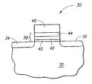
- FIG. 2 is a simplified side view, in section, of a Schottky source electrode memory cell incorporating a SONOS gate structure, in accordance with an embodiment of the present invention.
- MOS FETs metal-oxide-semiconductor field effect transistors
- Schottky source side injection mechanisms in MOS FET structures have been created using cobalt silicide Schottky source contacts, as is described, for example, in “Enhancement of Hot-Electron Generation Rate In Schottky Source Metal-Oxide-Semiconductor Field Effect Transistors”, by K. Uchida et al., Applied Physics Letters, Vol. 76, No. 26, Jun. 26, 2000, pp. 3992-4.
- Dual gate structures for hot electron generation have been employed in electrically erasable memory cells, as is described, for example, in “Analysis Of The Hot-Electron Injection In Split-Gate Transistors Useful For EEPROM Applications”, by J. van Houdt et al. (IEEE Trans. EI. Dev., Vol. 39, No. 5, May 1992, pp. 1150-1156, IEEE Cat. No. 0018-9383).
- NOR memory cells provide advantages of small cell size with simplicity in processing.
- Such NOR memory cells are described, for example, in “IEEE Standard Definitions And Characterization of Floating Gate Semiconductor Arrays”, IEEE Cat. No. 1005-1998 (inst. of Elect. and Electr. Engrs., 345 E. 47 th St., New York N.Y. 10017-2394, USA, copyright 1999).
- a description of a T-cell flash EEPROM cell also known as a NOR cell, begins on p. 46. Such cells can be made to be extremely compact.
- FIG. 1 is a simplified side view, in section, of a Schottky source electrode memory transistor 10 formed on a semiconductive substrate 12 , in accordance with an embodiment of the present invention.
- semiconductor substrate or “semiconductive substrate” is defined to mean any construction comprising semiconductive material, including, but not limited to, bulk semiconductive materials such as a semiconductive wafer (either alone or in assemblies comprising other materials thereon), and semiconductive material layers (either alone or in assemblies comprising other materials).
- substrate refers to any supporting structure, including, but not limited to, the semiconductive substrates described above.
- the memory transistor 10 includes a Schottky source/drain contact 14 and another source/drain contact 16 respectively disposed on opposing edges of a memory gate 17 .
- both source/drain contacts 14 , 16 are Schottky contacts. In one embodiment, at least one of the source/drain contacts 14 , 16 forms a hole-conductive Schottky contact. In one embodiment, at least one of the source/drain contacts 14 , 16 forms an electron-conductive Schottky contact. In one embodiment, one of the source/drain contacts 14 , 16 is a conventional diffused or implanted ohmic contact while the other is a Schottky contact. In one embodiment, one or both of the source/drain contacts 14 , 16 is spaced apart from the memory gate structure 17 . In one embodiment, at least one of the source/drain contacts 14 , 16 comprises a cobalt silicide Schottky contact. In one embodiment, at least one of the source/drain contacts 14 , 16 , comprises a material taken from Table I below.
- the memory gate structure 17 includes a first gate dielectric 18 .
- a conventional gate dielectric formed by oxidation of semiconductor material forms the first gate dielectric 18 .
- the memory gate structure 17 also includes a conductive gate 20 formed atop the first gate dielectric 18 .
- the conductive gate 20 is formed from conventional polycrystalline silicon or polysilicon.
- the memory gate structure 17 includes a second gate dielectric 22 formed atop the conductive gate 20 by any conventional process. In one embodiment, the memory gate structure 17 further includes a control gate 24 . In one embodiment, the control gate 24 comprises conductive material. In one embodiment, the control gate 24 comprises conventional polycrystalline silicon.
- the memory transistor 10 is programmed by application of suitable biases to the control gate 24 and the source/drain contacts 14 , 16 .
- a known amount of charge is transferred into the conductive gate structure 20 .
- charge transfer is effectuated via hot charge carriers and with efficiencies of up to four orders of magnitude greater than previous devices. In turn, such permits data storage with greatly reduced total power consumption. This promotes increased operating life of the memory transistor 10 .
- the memory transistor 10 may be programmed to any of multiple charge storage states, in accordance with conventional flash memory device practices. As a result, it is possible to store more than one bit in each of memory transistors 10 .
- the memory transistor 10 may also be “deprogrammed” by application of suitable biases in known fashions.
- FIG. 2 is a simplified side view, in section, of a Schottky source/drain electrode memory transistor 30 formed on a semiconductive substrate 32 , in accordance with an embodiment of the present invention.
- the memory transistor 30 includes source/drain contacts 34 , 36 , analogous to source/drain contacts 14 , 16 of FIG. 1 .
- a SONOS gate dielectric 38 is formed between the source/drain electrodes 34 , 36 .
- a SONOS gate dielectric 38 typically includes multiple dielectric layers 40 , 42 , 44 .
- such a SONOS gate dielectric may comprise Silicon (e.g., substrate 32 ), Oxide (e.g., dielectric layer 40 ), Nitride (e.g., dielectric layer 42 ) and Oxide (e.g., dielectric layer 44 ).
- a conductive gate 46 is formed thereatop, and such may comprise Silicon, providing a conventional SONOS structure.
- the memory transistor 30 differs from the memory transistor 10 of FIG. 1 in that spatially distinct charge distribution patterns are possible. For example, one set of bias conditions results in charge carriers being preferentially stored in the gate dielectric 38 adjacent source/drain contact 34 , while a different set of bias conditions results in charge carriers being stored adjacent source/drain contact 36 . These options are not mutually exclusive, and, as a result, a minimum of four measurably distinct charge storage patterns are possible in each memory transistor 30 . Again, conventional bias techniques allow deprogramming of each memory transistor 30 . Additionally, flash memory techniques allow discrimination between different quantities of charge that may be stored in each location.
Abstract
Description
| TABLE I |
| Schottky contact barrier heights on p- and n-type |
| silicon (from “Semiconductor Devices and Integrated |
| Electronics”, A. G. Milnes, Van Nostrand Reinhold Co., |
| copyright 1980, p. 100). |
| Metal | φm (eV) | φBp (eV) | φBn (eV) | φBp + φBn (eV) | ||
| Au | 4.8 | 0.34 | 0.81 | 1.15 | ||
| Ni | 4.5 | 0.50 | 0.66 | 1.16 | ||
| Cu | 4.4 | 0.46 | 0.69 | 1.14 | ||
| Ag | 4.3 | 0.53 | 0.69 | 1.22 | ||
| Al | 4.25 | 0.57 | 0.68 | 1.25 | ||
| Pb | 4.0 | 0.54 | 0.6 | 1.14 | ||
| Hf | 3.5 | 0.63 | — | — | ||
| CoSi | — | 0.38 | 0.68 | 1.06 | ||
Claims (30)
Priority Applications (4)
| Application Number | Priority Date | Filing Date | Title |
|---|---|---|---|
| US10/215,898 US6835619B2 (en) | 2002-08-08 | 2002-08-08 | Method of forming a memory transistor comprising a Schottky contact |
| US10/393,129 US6791140B2 (en) | 2002-08-08 | 2003-03-19 | Memory transistor structure |
| US11/023,719 US7745283B2 (en) | 2002-08-08 | 2004-12-28 | Method of fabricating memory transistor |
| US11/648,200 US7651911B2 (en) | 2002-08-08 | 2006-12-29 | Memory transistor and methods |
Applications Claiming Priority (1)
| Application Number | Priority Date | Filing Date | Title |
|---|---|---|---|
| US10/215,898 US6835619B2 (en) | 2002-08-08 | 2002-08-08 | Method of forming a memory transistor comprising a Schottky contact |
Related Child Applications (2)
| Application Number | Title | Priority Date | Filing Date |
|---|---|---|---|
| US10/393,129 Division US6791140B2 (en) | 2002-08-08 | 2003-03-19 | Memory transistor structure |
| US11/023,719 Continuation US7745283B2 (en) | 2002-08-08 | 2004-12-28 | Method of fabricating memory transistor |
Publications (2)
| Publication Number | Publication Date |
|---|---|
| US20040029322A1 US20040029322A1 (en) | 2004-02-12 |
| US6835619B2 true US6835619B2 (en) | 2004-12-28 |
Family
ID=31494963
Family Applications (4)
| Application Number | Title | Priority Date | Filing Date |
|---|---|---|---|
| US10/215,898 Expired - Lifetime US6835619B2 (en) | 2002-08-08 | 2002-08-08 | Method of forming a memory transistor comprising a Schottky contact |
| US10/393,129 Expired - Lifetime US6791140B2 (en) | 2002-08-08 | 2003-03-19 | Memory transistor structure |
| US11/023,719 Expired - Lifetime US7745283B2 (en) | 2002-08-08 | 2004-12-28 | Method of fabricating memory transistor |
| US11/648,200 Expired - Lifetime US7651911B2 (en) | 2002-08-08 | 2006-12-29 | Memory transistor and methods |
Family Applications After (3)
| Application Number | Title | Priority Date | Filing Date |
|---|---|---|---|
| US10/393,129 Expired - Lifetime US6791140B2 (en) | 2002-08-08 | 2003-03-19 | Memory transistor structure |
| US11/023,719 Expired - Lifetime US7745283B2 (en) | 2002-08-08 | 2004-12-28 | Method of fabricating memory transistor |
| US11/648,200 Expired - Lifetime US7651911B2 (en) | 2002-08-08 | 2006-12-29 | Memory transistor and methods |
Country Status (1)
| Country | Link |
|---|---|
| US (4) | US6835619B2 (en) |
Cited By (4)
| Publication number | Priority date | Publication date | Assignee | Title |
|---|---|---|---|---|
| US20050122787A1 (en) * | 2002-08-08 | 2005-06-09 | Prall Kirk D. | Memory transistor and methods |
| US20080099808A1 (en) * | 2006-10-31 | 2008-05-01 | Burnett James D | One transistor dram cell structure and method for forming |
| CN101807578A (en) * | 2010-03-16 | 2010-08-18 | 复旦大学 | Charge-captured non-volatilization semiconductor memory and manufacturing method thereof |
| WO2011091707A1 (en) * | 2010-01-29 | 2011-08-04 | 复旦大学 | Charge capturing non-volatile semiconductor memory and manufacturing method thereof |
Families Citing this family (8)
| Publication number | Priority date | Publication date | Assignee | Title |
|---|---|---|---|---|
| KR20040037327A (en) * | 2002-10-28 | 2004-05-07 | 삼성전자주식회사 | Nonvolatile memory device having asymmetric source/drain region and fabricating method thereof |
| US7109532B1 (en) * | 2003-12-23 | 2006-09-19 | Lee Zachary K | High Ion/Ioff SOI MOSFET using body voltage control |
| US7446371B2 (en) * | 2004-10-21 | 2008-11-04 | Samsung Electronics Co., Ltd. | Non-volatile memory cell structure with charge trapping layers and method of fabricating the same |
| US20080128786A1 (en) * | 2006-12-04 | 2008-06-05 | Electronics And Telecommunications Research Institute | High density semiconductor memory device and method for manufacturing the same |
| US7829929B2 (en) * | 2008-02-19 | 2010-11-09 | Samsung Electronics Co., Ltd. | Non-volatile memory device and non-volatile semiconductor integrated circuit device, including the same |
| CN101777562B (en) * | 2010-01-15 | 2015-05-20 | 复旦大学 | Non-volatile semiconductor memory with floating gate and manufacturing method thereof |
| US9444041B2 (en) * | 2013-03-15 | 2016-09-13 | Globalfoundries Singapore Pte. Ltd. | Back-gated non-volatile memory cell |
| KR102415409B1 (en) * | 2015-09-09 | 2022-07-04 | 에스케이하이닉스 주식회사 | EPROM cell, method of fabricating the EPROM cell, and EPROM cell array |
Citations (8)
| Publication number | Priority date | Publication date | Assignee | Title |
|---|---|---|---|---|
| US5990509A (en) | 1997-01-22 | 1999-11-23 | International Business Machines Corporation | 2F-square memory cell for gigabit memory applications |
| US6141248A (en) * | 1999-07-29 | 2000-10-31 | Micron Technology, Inc. | DRAM and SRAM memory cells with repressed memory |
| US6144093A (en) | 1998-04-27 | 2000-11-07 | International Rectifier Corp. | Commonly housed diverse semiconductor die with reduced inductance |
| JP2001007229A (en) * | 1999-06-25 | 2001-01-12 | Toshiba Corp | Semiconductor device |
| US6303479B1 (en) * | 1999-12-16 | 2001-10-16 | Spinnaker Semiconductor, Inc. | Method of manufacturing a short-channel FET with Schottky-barrier source and drain contacts |
| US6320223B1 (en) | 1999-03-18 | 2001-11-20 | U.S. Philips Corporation | Electronic device comprising a trench gate field effect device |
| US6331467B1 (en) | 1999-03-30 | 2001-12-18 | U.S. Philips Corporation | Method of manufacturing a trench gate field effect semiconductor device |
| US20020163032A1 (en) * | 2001-05-03 | 2002-11-07 | Horng-Chih Lin | Nonvolatile memory and method of manufacturing the same |
Family Cites Families (25)
| Publication number | Priority date | Publication date | Assignee | Title |
|---|---|---|---|---|
| US4139781A (en) * | 1974-08-13 | 1979-02-13 | Honeywell Inc. | Logic gate circuits |
| US4796069A (en) * | 1981-05-13 | 1989-01-03 | International Business Machines Corporation | Schottky diode having limited area self-aligned guard ring and method for making same |
| US4811078A (en) * | 1985-05-01 | 1989-03-07 | Texas Instruments Incorporated | Integrated circuit device and process with tin capacitors |
| US5216264A (en) * | 1989-06-07 | 1993-06-01 | Sharp Kabushiki Kaisha | Silicon carbide MOS type field-effect transistor with at least one of the source and drain regions is formed by the use of a schottky contact |
| US5355007A (en) * | 1990-11-23 | 1994-10-11 | Texas Instruments Incorporated | Devices for non-volatile memory, systems and methods |
| BE1007902A3 (en) * | 1993-12-23 | 1995-11-14 | Philips Electronics Nv | Switching element with memory with schottky barrier tunnel. |
| JP3460095B2 (en) * | 1994-06-01 | 2003-10-27 | 富士通株式会社 | Ferroelectric memory |
| US5768192A (en) * | 1996-07-23 | 1998-06-16 | Saifun Semiconductors, Ltd. | Non-volatile semiconductor memory cell utilizing asymmetrical charge trapping |
| KR100238199B1 (en) * | 1996-07-30 | 2000-01-15 | 윤종용 | Flash eeprom device and manufacturing method thereof |
| TW468253B (en) * | 1997-01-13 | 2001-12-11 | Hitachi Ltd | Semiconductor memory device |
| JP3532747B2 (en) | 1997-12-09 | 2004-05-31 | 富士通株式会社 | Ferroelectric storage device, flash memory, and nonvolatile random access memory |
| EP1177576A2 (en) * | 1999-03-31 | 2002-02-06 | SiCED Electronics Development GmbH & Co KG | Integrated semiconductor device with one lateral power gate |
| US6339005B1 (en) * | 1999-10-22 | 2002-01-15 | International Business Machines Corporation | Disposable spacer for symmetric and asymmetric Schottky contact to SOI MOSFET |
| JP2001196661A (en) * | 1999-10-27 | 2001-07-19 | Sony Corp | Magnetization control method, information storage method, magnetic function element, and information storage element |
| US6617642B1 (en) * | 2000-02-23 | 2003-09-09 | Tripath Technology, Inc. | Field effect transistor structure for driving inductive loads |
| WO2001080410A1 (en) * | 2000-04-13 | 2001-10-25 | Infineon Technologies Ag | Voltage transformer |
| KR100821456B1 (en) * | 2000-08-14 | 2008-04-11 | 샌디스크 쓰리디 엘엘씨 | Dense arrays and charge storage devices, and methods for making same |
| US6998678B2 (en) * | 2001-05-17 | 2006-02-14 | Infineon Technologies Ag | Semiconductor arrangement with a MOS-transistor and a parallel Schottky-diode |
| DE10135870C1 (en) * | 2001-07-24 | 2003-02-20 | Infineon Technologies Ag | Production of an integrated semiconductor circuit comprises depositing layer sequence, anisotropically etching, oxidizing the lowermost layer of the layer sequence, depositing further layer sequence on substrate, and isotropically etching |
| US6529034B1 (en) * | 2001-11-07 | 2003-03-04 | International Rectifier Corporation | Integrated series schottky and FET to allow negative drain voltage |
| US6562706B1 (en) * | 2001-12-03 | 2003-05-13 | Industrial Technology Research Institute | Structure and manufacturing method of SiC dual metal trench Schottky diode |
| US6806630B2 (en) * | 2002-01-09 | 2004-10-19 | Hewlett-Packard Development Company, L.P. | Electron emitter device for data storage applications and method of manufacture |
| US6835619B2 (en) * | 2002-08-08 | 2004-12-28 | Micron Technology, Inc. | Method of forming a memory transistor comprising a Schottky contact |
| US6833556B2 (en) * | 2002-08-12 | 2004-12-21 | Acorn Technologies, Inc. | Insulated gate field effect transistor having passivated schottky barriers to the channel |
| US20050248365A1 (en) * | 2004-05-07 | 2005-11-10 | Chang Augustine W | Distributive computing subsystem of generic IC parts |
-
2002
- 2002-08-08 US US10/215,898 patent/US6835619B2/en not_active Expired - Lifetime
-
2003
- 2003-03-19 US US10/393,129 patent/US6791140B2/en not_active Expired - Lifetime
-
2004
- 2004-12-28 US US11/023,719 patent/US7745283B2/en not_active Expired - Lifetime
-
2006
- 2006-12-29 US US11/648,200 patent/US7651911B2/en not_active Expired - Lifetime
Patent Citations (8)
| Publication number | Priority date | Publication date | Assignee | Title |
|---|---|---|---|---|
| US5990509A (en) | 1997-01-22 | 1999-11-23 | International Business Machines Corporation | 2F-square memory cell for gigabit memory applications |
| US6144093A (en) | 1998-04-27 | 2000-11-07 | International Rectifier Corp. | Commonly housed diverse semiconductor die with reduced inductance |
| US6320223B1 (en) | 1999-03-18 | 2001-11-20 | U.S. Philips Corporation | Electronic device comprising a trench gate field effect device |
| US6331467B1 (en) | 1999-03-30 | 2001-12-18 | U.S. Philips Corporation | Method of manufacturing a trench gate field effect semiconductor device |
| JP2001007229A (en) * | 1999-06-25 | 2001-01-12 | Toshiba Corp | Semiconductor device |
| US6141248A (en) * | 1999-07-29 | 2000-10-31 | Micron Technology, Inc. | DRAM and SRAM memory cells with repressed memory |
| US6303479B1 (en) * | 1999-12-16 | 2001-10-16 | Spinnaker Semiconductor, Inc. | Method of manufacturing a short-channel FET with Schottky-barrier source and drain contacts |
| US20020163032A1 (en) * | 2001-05-03 | 2002-11-07 | Horng-Chih Lin | Nonvolatile memory and method of manufacturing the same |
Non-Patent Citations (15)
Cited By (10)
| Publication number | Priority date | Publication date | Assignee | Title |
|---|---|---|---|---|
| US20050122787A1 (en) * | 2002-08-08 | 2005-06-09 | Prall Kirk D. | Memory transistor and methods |
| US20070111443A1 (en) * | 2002-08-08 | 2007-05-17 | Prall Kirk D | Memory transistor and methods |
| US7651911B2 (en) * | 2002-08-08 | 2010-01-26 | Micron Technology, Inc. | Memory transistor and methods |
| US7745283B2 (en) * | 2002-08-08 | 2010-06-29 | Micron Technology, Inc. | Method of fabricating memory transistor |
| US20080099808A1 (en) * | 2006-10-31 | 2008-05-01 | Burnett James D | One transistor dram cell structure and method for forming |
| US7608898B2 (en) * | 2006-10-31 | 2009-10-27 | Freescale Semiconductor, Inc. | One transistor DRAM cell structure |
| US20100001326A1 (en) * | 2006-10-31 | 2010-01-07 | Freescale Semiconductor, Inc. | One transistor dram cell structure and method for forming |
| US8283244B2 (en) | 2006-10-31 | 2012-10-09 | Freescale Semiconductor, Inc. | Method for forming one transistor DRAM cell structure |
| WO2011091707A1 (en) * | 2010-01-29 | 2011-08-04 | 复旦大学 | Charge capturing non-volatile semiconductor memory and manufacturing method thereof |
| CN101807578A (en) * | 2010-03-16 | 2010-08-18 | 复旦大学 | Charge-captured non-volatilization semiconductor memory and manufacturing method thereof |
Also Published As
| Publication number | Publication date |
|---|---|
| US20050122787A1 (en) | 2005-06-09 |
| US7651911B2 (en) | 2010-01-26 |
| US6791140B2 (en) | 2004-09-14 |
| US20040029370A1 (en) | 2004-02-12 |
| US7745283B2 (en) | 2010-06-29 |
| US20070111443A1 (en) | 2007-05-17 |
| US20040029322A1 (en) | 2004-02-12 |
Similar Documents
| Publication | Publication Date | Title |
|---|---|---|
| US7651911B2 (en) | Memory transistor and methods | |
| US7485513B2 (en) | One-device non-volatile random access memory cell | |
| US7176073B2 (en) | Methods of forming memory cells having diodes and electrode plates connected to source/drain regions | |
| US7257022B2 (en) | Nanocrystal write once read only memory for archival storage | |
| US7440317B2 (en) | One transistor SOI non-volatile random access memory cell | |
| US6808169B2 (en) | Non-volatile memory with crown electrode to increase capacitance between control gate and floating gate | |
| US6714436B1 (en) | Write operation for capacitorless RAM | |
| US6730960B2 (en) | Static NVRAM with ultra thin tunnel oxides | |
| US7166509B2 (en) | Write once read only memory with large work function floating gates | |
| US7315060B2 (en) | Semiconductor storage device, manufacturing method therefor and portable electronic equipment | |
| US10134738B2 (en) | Low power memory device with JFET device structures | |
| JP2000340679A (en) | Body contact type dynamic memory | |
| TW200834886A (en) | One transistor DRAM cell structure and method for forming | |
| US7544993B2 (en) | Semiconductor storage device and portable electronic equipment | |
| KR20110094213A (en) | Jfet device structures and methods for fabricating the same | |
| Joodaki | Selected advances in nanoelectronic devices: logic, memory and RF | |
| US20070007510A1 (en) | Stackable memory device and organic transistor structure | |
| JP3541331B2 (en) | Ferroelectric memory cell | |
| JP2004349353A (en) | Semiconductor storage device, its operating method, and portable electronic equipment |
Legal Events
| Date | Code | Title | Description |
|---|---|---|---|
| AS | Assignment |
Owner name: MICRON TECHNOLOGY, INC., IDAHO Free format text: ASSIGNMENT OF ASSIGNORS INTEREST;ASSIGNOR:PRALL, KIRK D.;REEL/FRAME:013188/0278 Effective date: 20020802 |
|
| FEPP | Fee payment procedure |
Free format text: PAYOR NUMBER ASSIGNED (ORIGINAL EVENT CODE: ASPN); ENTITY STATUS OF PATENT OWNER: LARGE ENTITY |
|
| STCF | Information on status: patent grant |
Free format text: PATENTED CASE |
|
| CC | Certificate of correction | ||
| FPAY | Fee payment |
Year of fee payment: 4 |
|
| FPAY | Fee payment |
Year of fee payment: 8 |
|
| AS | Assignment |
Owner name: U.S. BANK NATIONAL ASSOCIATION, AS COLLATERAL AGENT, CALIFORNIA Free format text: SECURITY INTEREST;ASSIGNOR:MICRON TECHNOLOGY, INC.;REEL/FRAME:038669/0001 Effective date: 20160426 Owner name: U.S. BANK NATIONAL ASSOCIATION, AS COLLATERAL AGEN Free format text: SECURITY INTEREST;ASSIGNOR:MICRON TECHNOLOGY, INC.;REEL/FRAME:038669/0001 Effective date: 20160426 |
|
| AS | Assignment |
Owner name: MORGAN STANLEY SENIOR FUNDING, INC., AS COLLATERAL AGENT, MARYLAND Free format text: PATENT SECURITY AGREEMENT;ASSIGNOR:MICRON TECHNOLOGY, INC.;REEL/FRAME:038954/0001 Effective date: 20160426 Owner name: MORGAN STANLEY SENIOR FUNDING, INC., AS COLLATERAL Free format text: PATENT SECURITY AGREEMENT;ASSIGNOR:MICRON TECHNOLOGY, INC.;REEL/FRAME:038954/0001 Effective date: 20160426 |
|
| FPAY | Fee payment |
Year of fee payment: 12 |
|
| AS | Assignment |
Owner name: U.S. BANK NATIONAL ASSOCIATION, AS COLLATERAL AGENT, CALIFORNIA Free format text: CORRECTIVE ASSIGNMENT TO CORRECT THE REPLACE ERRONEOUSLY FILED PATENT #7358718 WITH THE CORRECT PATENT #7358178 PREVIOUSLY RECORDED ON REEL 038669 FRAME 0001. ASSIGNOR(S) HEREBY CONFIRMS THE SECURITY INTEREST;ASSIGNOR:MICRON TECHNOLOGY, INC.;REEL/FRAME:043079/0001 Effective date: 20160426 Owner name: U.S. BANK NATIONAL ASSOCIATION, AS COLLATERAL AGEN Free format text: CORRECTIVE ASSIGNMENT TO CORRECT THE REPLACE ERRONEOUSLY FILED PATENT #7358718 WITH THE CORRECT PATENT #7358178 PREVIOUSLY RECORDED ON REEL 038669 FRAME 0001. ASSIGNOR(S) HEREBY CONFIRMS THE SECURITY INTEREST;ASSIGNOR:MICRON TECHNOLOGY, INC.;REEL/FRAME:043079/0001 Effective date: 20160426 |
|
| AS | Assignment |
Owner name: JPMORGAN CHASE BANK, N.A., AS COLLATERAL AGENT, ILLINOIS Free format text: SECURITY INTEREST;ASSIGNORS:MICRON TECHNOLOGY, INC.;MICRON SEMICONDUCTOR PRODUCTS, INC.;REEL/FRAME:047540/0001 Effective date: 20180703 Owner name: JPMORGAN CHASE BANK, N.A., AS COLLATERAL AGENT, IL Free format text: SECURITY INTEREST;ASSIGNORS:MICRON TECHNOLOGY, INC.;MICRON SEMICONDUCTOR PRODUCTS, INC.;REEL/FRAME:047540/0001 Effective date: 20180703 |
|
| AS | Assignment |
Owner name: MICRON TECHNOLOGY, INC., IDAHO Free format text: RELEASE BY SECURED PARTY;ASSIGNOR:U.S. BANK NATIONAL ASSOCIATION, AS COLLATERAL AGENT;REEL/FRAME:047243/0001 Effective date: 20180629 |
|
| AS | Assignment |
Owner name: MICRON TECHNOLOGY, INC., IDAHO Free format text: RELEASE BY SECURED PARTY;ASSIGNOR:MORGAN STANLEY SENIOR FUNDING, INC., AS COLLATERAL AGENT;REEL/FRAME:050937/0001 Effective date: 20190731 |
|
| AS | Assignment |
Owner name: MICRON SEMICONDUCTOR PRODUCTS, INC., IDAHO Free format text: RELEASE BY SECURED PARTY;ASSIGNOR:JPMORGAN CHASE BANK, N.A., AS COLLATERAL AGENT;REEL/FRAME:051028/0001 Effective date: 20190731 Owner name: MICRON TECHNOLOGY, INC., IDAHO Free format text: RELEASE BY SECURED PARTY;ASSIGNOR:JPMORGAN CHASE BANK, N.A., AS COLLATERAL AGENT;REEL/FRAME:051028/0001 Effective date: 20190731 |