US6855954B1 - Thin film transistor, fabrication method thereof and liquid crystal display having the thin film transistor - Google Patents
Thin film transistor, fabrication method thereof and liquid crystal display having the thin film transistor Download PDFInfo
- Publication number
- US6855954B1 US6855954B1 US09/619,556 US61955600A US6855954B1 US 6855954 B1 US6855954 B1 US 6855954B1 US 61955600 A US61955600 A US 61955600A US 6855954 B1 US6855954 B1 US 6855954B1
- Authority
- US
- United States
- Prior art keywords
- insulating layer
- film
- gate
- semiconductor film
- channel protection
- Prior art date
- Legal status (The legal status is an assumption and is not a legal conclusion. Google has not performed a legal analysis and makes no representation as to the accuracy of the status listed.)
- Expired - Lifetime, expires
Links
- 239000010409 thin film Substances 0.000 title claims abstract description 85
- 239000004973 liquid crystal related substance Substances 0.000 title claims abstract description 50
- 238000004519 manufacturing process Methods 0.000 title claims abstract description 39
- 238000000034 method Methods 0.000 title abstract description 107
- 239000010408 film Substances 0.000 claims abstract description 281
- 239000004065 semiconductor Substances 0.000 claims abstract description 63
- 239000000758 substrate Substances 0.000 claims abstract description 55
- 239000010410 layer Substances 0.000 claims description 220
- 230000003071 parasitic effect Effects 0.000 claims description 20
- 239000011159 matrix material Substances 0.000 claims description 7
- 238000010030 laminating Methods 0.000 claims description 4
- 239000000463 material Substances 0.000 claims description 4
- 238000010586 diagram Methods 0.000 description 34
- 229910004205 SiNX Inorganic materials 0.000 description 33
- VYPSYNLAJGMNEJ-UHFFFAOYSA-N Silicium dioxide Chemical compound O=[Si]=O VYPSYNLAJGMNEJ-UHFFFAOYSA-N 0.000 description 33
- 229910021417 amorphous silicon Inorganic materials 0.000 description 21
- 238000000206 photolithography Methods 0.000 description 20
- 239000012535 impurity Substances 0.000 description 19
- 230000002093 peripheral effect Effects 0.000 description 17
- 229910052681 coesite Inorganic materials 0.000 description 16
- 229910052906 cristobalite Inorganic materials 0.000 description 16
- 239000011521 glass Substances 0.000 description 16
- 238000000623 plasma-assisted chemical vapour deposition Methods 0.000 description 16
- 239000000377 silicon dioxide Substances 0.000 description 16
- 229910052682 stishovite Inorganic materials 0.000 description 16
- 229910052905 tridymite Inorganic materials 0.000 description 16
- 238000001020 plasma etching Methods 0.000 description 14
- 239000011229 interlayer Substances 0.000 description 12
- 238000004544 sputter deposition Methods 0.000 description 11
- 238000000059 patterning Methods 0.000 description 10
- 229920002120 photoresistant polymer Polymers 0.000 description 10
- 238000001039 wet etching Methods 0.000 description 9
- 238000000151 deposition Methods 0.000 description 8
- 238000003860 storage Methods 0.000 description 8
- 238000005530 etching Methods 0.000 description 7
- 229920001721 polyimide Polymers 0.000 description 7
- 239000011347 resin Substances 0.000 description 7
- 229920005989 resin Polymers 0.000 description 7
- 229910018125 Al-Si Inorganic materials 0.000 description 6
- 229910018520 Al—Si Inorganic materials 0.000 description 6
- UFHFLCQGNIYNRP-UHFFFAOYSA-N Hydrogen Chemical compound [H][H] UFHFLCQGNIYNRP-UHFFFAOYSA-N 0.000 description 6
- 239000003990 capacitor Substances 0.000 description 6
- 229910052739 hydrogen Inorganic materials 0.000 description 6
- 239000001257 hydrogen Substances 0.000 description 6
- 238000009413 insulation Methods 0.000 description 6
- 229910021420 polycrystalline silicon Inorganic materials 0.000 description 6
- 229920005591 polysilicon Polymers 0.000 description 6
- 101710190981 50S ribosomal protein L6 Proteins 0.000 description 5
- 239000004642 Polyimide Substances 0.000 description 5
- NIXOWILDQLNWCW-UHFFFAOYSA-N acrylic acid group Chemical group C(C=C)(=O)O NIXOWILDQLNWCW-UHFFFAOYSA-N 0.000 description 5
- 150000002500 ions Chemical class 0.000 description 5
- 229910052751 metal Inorganic materials 0.000 description 5
- 239000002184 metal Substances 0.000 description 5
- 239000011248 coating agent Substances 0.000 description 4
- 238000000576 coating method Methods 0.000 description 4
- 230000008021 deposition Effects 0.000 description 4
- 238000005070 sampling Methods 0.000 description 4
- 125000006850 spacer group Chemical group 0.000 description 4
- 238000001312 dry etching Methods 0.000 description 3
- 239000007789 gas Substances 0.000 description 3
- 230000007774 longterm Effects 0.000 description 3
- 229910052750 molybdenum Inorganic materials 0.000 description 3
- 229910052715 tantalum Inorganic materials 0.000 description 3
- 229920000178 Acrylic resin Polymers 0.000 description 2
- 239000004925 Acrylic resin Substances 0.000 description 2
- 229910000838 Al alloy Inorganic materials 0.000 description 2
- 229910052782 aluminium Inorganic materials 0.000 description 2
- XAGFODPZIPBFFR-UHFFFAOYSA-N aluminium Chemical compound [Al] XAGFODPZIPBFFR-UHFFFAOYSA-N 0.000 description 2
- 229910052796 boron Inorganic materials 0.000 description 2
- 230000015556 catabolic process Effects 0.000 description 2
- 238000005229 chemical vapour deposition Methods 0.000 description 2
- 238000006731 degradation reaction Methods 0.000 description 2
- AMGQUBHHOARCQH-UHFFFAOYSA-N indium;oxotin Chemical compound [In].[Sn]=O AMGQUBHHOARCQH-UHFFFAOYSA-N 0.000 description 2
- 238000010849 ion bombardment Methods 0.000 description 2
- 230000001678 irradiating effect Effects 0.000 description 2
- 229910052698 phosphorus Inorganic materials 0.000 description 2
- 239000003566 sealing material Substances 0.000 description 2
- 238000000926 separation method Methods 0.000 description 2
- 239000000126 substance Substances 0.000 description 2
- 230000001360 synchronised effect Effects 0.000 description 2
- ZOXJGFHDIHLPTG-UHFFFAOYSA-N Boron Chemical compound [B] ZOXJGFHDIHLPTG-UHFFFAOYSA-N 0.000 description 1
- VYZAMTAEIAYCRO-UHFFFAOYSA-N Chromium Chemical compound [Cr] VYZAMTAEIAYCRO-UHFFFAOYSA-N 0.000 description 1
- ZOKXTWBITQBERF-UHFFFAOYSA-N Molybdenum Chemical compound [Mo] ZOKXTWBITQBERF-UHFFFAOYSA-N 0.000 description 1
- OAICVXFJPJFONN-UHFFFAOYSA-N Phosphorus Chemical compound [P] OAICVXFJPJFONN-UHFFFAOYSA-N 0.000 description 1
- 229910052581 Si3N4 Inorganic materials 0.000 description 1
- 230000004913 activation Effects 0.000 description 1
- 229910045601 alloy Inorganic materials 0.000 description 1
- 239000000956 alloy Substances 0.000 description 1
- 230000015572 biosynthetic process Effects 0.000 description 1
- 230000000694 effects Effects 0.000 description 1
- 239000007772 electrode material Substances 0.000 description 1
- 238000002347 injection Methods 0.000 description 1
- 239000007924 injection Substances 0.000 description 1
- 239000011733 molybdenum Substances 0.000 description 1
- 239000011574 phosphorus Substances 0.000 description 1
- 238000005268 plasma chemical vapour deposition Methods 0.000 description 1
- 239000009719 polyimide resin Substances 0.000 description 1
- HQVNEWCFYHHQES-UHFFFAOYSA-N silicon nitride Chemical compound N12[Si]34N5[Si]62N3[Si]51N64 HQVNEWCFYHHQES-UHFFFAOYSA-N 0.000 description 1
- 229910052814 silicon oxide Inorganic materials 0.000 description 1
- 239000002356 single layer Substances 0.000 description 1
- GUVRBAGPIYLISA-UHFFFAOYSA-N tantalum atom Chemical compound [Ta] GUVRBAGPIYLISA-UHFFFAOYSA-N 0.000 description 1
Images


Classifications
-
- G—PHYSICS
- G02—OPTICS
- G02F—OPTICAL DEVICES OR ARRANGEMENTS FOR THE CONTROL OF LIGHT BY MODIFICATION OF THE OPTICAL PROPERTIES OF THE MEDIA OF THE ELEMENTS INVOLVED THEREIN; NON-LINEAR OPTICS; FREQUENCY-CHANGING OF LIGHT; OPTICAL LOGIC ELEMENTS; OPTICAL ANALOGUE/DIGITAL CONVERTERS
- G02F1/00—Devices or arrangements for the control of the intensity, colour, phase, polarisation or direction of light arriving from an independent light source, e.g. switching, gating or modulating; Non-linear optics
- G02F1/01—Devices or arrangements for the control of the intensity, colour, phase, polarisation or direction of light arriving from an independent light source, e.g. switching, gating or modulating; Non-linear optics for the control of the intensity, phase, polarisation or colour
- G02F1/13—Devices or arrangements for the control of the intensity, colour, phase, polarisation or direction of light arriving from an independent light source, e.g. switching, gating or modulating; Non-linear optics for the control of the intensity, phase, polarisation or colour based on liquid crystals, e.g. single liquid crystal display cells
- G02F1/133—Constructional arrangements; Operation of liquid crystal cells; Circuit arrangements
- G02F1/136—Liquid crystal cells structurally associated with a semi-conducting layer or substrate, e.g. cells forming part of an integrated circuit
-
- H—ELECTRICITY
- H01—ELECTRIC ELEMENTS
- H01L—SEMICONDUCTOR DEVICES NOT COVERED BY CLASS H10
- H01L27/00—Devices consisting of a plurality of semiconductor or other solid-state components formed in or on a common substrate
- H01L27/02—Devices consisting of a plurality of semiconductor or other solid-state components formed in or on a common substrate including semiconductor components specially adapted for rectifying, oscillating, amplifying or switching and having at least one potential-jump barrier or surface barrier; including integrated passive circuit elements with at least one potential-jump barrier or surface barrier
- H01L27/12—Devices consisting of a plurality of semiconductor or other solid-state components formed in or on a common substrate including semiconductor components specially adapted for rectifying, oscillating, amplifying or switching and having at least one potential-jump barrier or surface barrier; including integrated passive circuit elements with at least one potential-jump barrier or surface barrier the substrate being other than a semiconductor body, e.g. an insulating body
- H01L27/1214—Devices consisting of a plurality of semiconductor or other solid-state components formed in or on a common substrate including semiconductor components specially adapted for rectifying, oscillating, amplifying or switching and having at least one potential-jump barrier or surface barrier; including integrated passive circuit elements with at least one potential-jump barrier or surface barrier the substrate being other than a semiconductor body, e.g. an insulating body comprising a plurality of TFTs formed on a non-semiconducting substrate, e.g. driving circuits for AMLCDs
-
- H—ELECTRICITY
- H01—ELECTRIC ELEMENTS
- H01L—SEMICONDUCTOR DEVICES NOT COVERED BY CLASS H10
- H01L29/00—Semiconductor devices adapted for rectifying, amplifying, oscillating or switching, or capacitors or resistors with at least one potential-jump barrier or surface barrier, e.g. PN junction depletion layer or carrier concentration layer; Details of semiconductor bodies or of electrodes thereof ; Multistep manufacturing processes therefor
- H01L29/66—Types of semiconductor device ; Multistep manufacturing processes therefor
- H01L29/66007—Multistep manufacturing processes
- H01L29/66075—Multistep manufacturing processes of devices having semiconductor bodies comprising group 14 or group 13/15 materials
- H01L29/66227—Multistep manufacturing processes of devices having semiconductor bodies comprising group 14 or group 13/15 materials the devices being controllable only by the electric current supplied or the electric potential applied, to an electrode which does not carry the current to be rectified, amplified or switched, e.g. three-terminal devices
- H01L29/66409—Unipolar field-effect transistors
- H01L29/66477—Unipolar field-effect transistors with an insulated gate, i.e. MISFET
- H01L29/66742—Thin film unipolar transistors
- H01L29/6675—Amorphous silicon or polysilicon transistors
- H01L29/66765—Lateral single gate single channel transistors with inverted structure, i.e. the channel layer is formed after the gate
-
- H—ELECTRICITY
- H01—ELECTRIC ELEMENTS
- H01L—SEMICONDUCTOR DEVICES NOT COVERED BY CLASS H10
- H01L29/00—Semiconductor devices adapted for rectifying, amplifying, oscillating or switching, or capacitors or resistors with at least one potential-jump barrier or surface barrier, e.g. PN junction depletion layer or carrier concentration layer; Details of semiconductor bodies or of electrodes thereof ; Multistep manufacturing processes therefor
- H01L29/66—Types of semiconductor device ; Multistep manufacturing processes therefor
- H01L29/68—Types of semiconductor device ; Multistep manufacturing processes therefor controllable by only the electric current supplied, or only the electric potential applied, to an electrode which does not carry the current to be rectified, amplified or switched
- H01L29/76—Unipolar devices, e.g. field effect transistors
- H01L29/772—Field effect transistors
- H01L29/78—Field effect transistors with field effect produced by an insulated gate
- H01L29/786—Thin film transistors, i.e. transistors with a channel being at least partly a thin film
- H01L29/78606—Thin film transistors, i.e. transistors with a channel being at least partly a thin film with supplementary region or layer in the thin film or in the insulated bulk substrate supporting it for controlling or increasing the safety of the device
- H01L29/78618—Thin film transistors, i.e. transistors with a channel being at least partly a thin film with supplementary region or layer in the thin film or in the insulated bulk substrate supporting it for controlling or increasing the safety of the device characterised by the drain or the source properties, e.g. the doping structure, the composition, the sectional shape or the contact structure
- H01L29/78621—Thin film transistors, i.e. transistors with a channel being at least partly a thin film with supplementary region or layer in the thin film or in the insulated bulk substrate supporting it for controlling or increasing the safety of the device characterised by the drain or the source properties, e.g. the doping structure, the composition, the sectional shape or the contact structure with LDD structure or an extension or an offset region or characterised by the doping profile
Definitions
- the present invention relates to a thin film transistor, a fabrication method thereof and a liquid crystal display having the thin film transistor.
- TFT thin film transistor
- a structure of the thin film transistor is divided roughly into the so-called bottom-gate-type inverted staggered structure in which a gate electrode is formed on a glass substrate side rather than source and drain electrodes side and the so-called top-gate-type staggered structure or planer-type structure in which the source and the drain electrodes are formed on a glass substrate side rather than a gate electrode.
- a bottom-gate-type thin film transistor can be further divided into two structures. One is a structure in which a channel protection film is formed on an operational semiconductor film forming a channel portion and the other is a structure in which a portion of an upper layer of the operational semiconductor film is etched without having the channel protection film.
- a cross sectional structure of the conventional bottom-gate-type thin film transistor having the channel protection film is described with reference to FIG. 21.
- a thin film transistor 100 has a bottom-gate-type gate electrode 104 formed on a glass substrate 102 .
- a gate insulating film 106 made of SiN x (silicon nitride) is formed on the gate electrode 104 and the glass substrate 100 .
- An operational semiconductor layer 108 made of, for example, amorphous silicon (a-Si:H; hereinafter, simply referred to as a-Si) is formed on the gate insulating film 106 , and a channel protection film 110 made of SiN x is formed on the operational semiconductor layer 108 on the gate electrode 104 .
- a-Si:H amorphous silicon
- An impurity semiconductor layer (ohmic semiconductor layer) 112 and source and drain electrodes 114 and 115 are formed running over opposing edge portions of the channel protection film 110 .
- the deposit from the gate insulating film 106 to the channel protection film 110 are sequentially formed by a plasma CVD method (PCVD method).
- An interlayer insulating film 116 is formed on the source electrode and the drain electrode 115 and on the channel protection film 110 exposed between the opposing edge portions of the source electrode 114 and the drain electrode and 115 .
- a contact hole is formed on the interlayer insulating film 116 on the source electrode 114 and a pixel electrode 118 formed on the interlayer insulating film 116 is connected with the source electrode 114 .
- the channel protection film 110 When forming the channel protection film 110 by patterning an inorganic insulating film, a back exposure is performed from the back side of the glass substrate 102 (lower part of FIG. 21 ). Thus, the channel protection film 110 is self-aligningly formed by using the gate electrode 104 as a mask.
- the source electrode 114 and the drain electrode 115 on the channel protection film 110 are separated taking a mask pattern positioning error in the photolithography process into consideration. Therefore, the source electrode 114 and the drain electrode 115 are structured so that the edge portions thereof respectively have overlapping areas shown by ⁇ L in the diagram with respect to the gate electrode 104 and face each other by running over the edge portions of the channel protection film 110 .
- a channel area of the operational semiconductor layer 108 is in an “ON” state with a low resistance when a voltage with a positive polarity is applied to the gate electrode 104 , and the channel area is in an “OFF” state with a high resistance when a voltage with a negative polarity is applied to the gate electrode 104 .
- the channel area is in an “ON” state with a low resistance when a voltage with a negative polarity is applied to the gate electrode 104 , and the channel area is in an “OFF” state with a high resistance when a voltage with a positive polarity is applied to the gate electrode 104 .
- a conduction (“ON”) state and cutoff (“OFF”) state of a thin film transistor can be controlled by applying a predetermined voltage to the gate electrode 104 .
- the parasitic capacitances Cp are in proportion to the inverse number of the overlapping length ⁇ L, overlapping width W, a relative dielectric constant ⁇ s of the channel protection film 110 , and a film thickness t s of the channel protection film 110 . It will be noted that ⁇ 0 is a vacuum dielectric constant.
- An active matrix type liquid crystal display using this thin film transistor as a switching element has a problem in which a pixel effective voltage is reduced due to a field-through voltage resulted from the parasitic capacitances Cp, thereby generating a degradation of picture quality such as flickering of the display, a reduction in contrast and the like.
- a slit is formed on the channel protection film (SiN x film) 10 by using an RIE (reactive ion etching). Therefore, permanent damages such as a trap level in a film and the like due to ion bombardment are generated to an SiN x film of the channel protection film 110 , and a possibility of a reduction in electric characteristics or a long-term reliability of the thin film transistor exists, thereby resulting in an obstacle for improving a fabrication yield.
- RIE reactive ion etching
- An object of the present invention is to provide a thin film transistor which is a bottom-gate-type thin film transistor in which a channel protection film is formed, suppresses the parasitic capacitances, and improves the fabrication yield, and to provide a fabrication method thereof and a liquid crystal display having the thin film transistor.
- a bottom gate type thin film transistor comprising a gate electrode formed on a substrate, a gate insulating film formed on the gate electrode, an operational semiconductor film formed on the gate insulating film on the gate electrode, a channel protection film formed on the operational semiconductor film, a source and a drain electrodes formed on both sides of a top surface of the channel protection film and connected to the operational semiconductor film, wherein the channel protection film comprises a first insulating layer contacting to an upper interface of the operational semiconductor film and a second insulating film formed on the first insulating layer.
- FIG. 1 a through FIG. 1 c are diagrams showing schematic structures of a thin film transistor according to an embodiment of the present invention.
- FIG. 2 a through FIG. 2 d are diagrams describing Example 1 in a fabrication process of a thin film transistor according to an embodiment of the present invention.
- FIG. 3 a through FIG. 3 c are diagrams describing Example 1 in a fabrication process of a thin film transistor according to an embodiment of the present invention.
- FIG. 4 a and FIG. 4 b are diagrams describing Example 1 in a fabrication process of a thin film transistor according to an embodiment of the present invention.
- FIG. 5 a and FIG. 5 b are diagrams describing Example 1 for an array substrate of a liquid crystal display panel fabricated by using a fabrication method of a thin film transistor according to an embodiment of the present invention.
- FIG. 6 a through FIG. 6 c are diagrams describing an example of a variation of Example 1 for a liquid crystal display according to an embodiment of the present invention.
- FIG. 7 is a diagram describing an example of a variation of Example 1 for a liquid crystal display according to an embodiment of the present invention.
- FIG. 8 is a diagram describing an example of another variation of Example 1 for a liquid crystal display according to an embodiment of the present invention.
- FIG. 9 a through FIG. 9 d are diagrams describing Example 2 in a fabrication process of a thin film transistor according to an embodiment of the present invention.
- FIG. 10 a through FIG. 10 c are diagrams describing Example 2 in a fabrication process of a thin film transistor according to an embodiment of the present invention.
- FIG. 11 a through FIG. 11 c are diagrams describing Example 2 in a fabrication process of a thin film transistor according to an embodiment of the present invention.
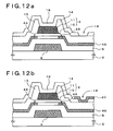
- FIG. 12 a and FIG. 12 b are diagrams describing Example 2 in a fabrication process of a thin film transistor according to an embodiment of the present invention.
- FIG. 13 is a diagram describing Example 2 for a liquid crystal display according to an embodiment of the present invention.
- FIG. 14 a through FIG. 14 d are diagrams describing Example 3 in a fabrication process of this thin film transistor according to an embodiment of the present invention.
- FIG. 15 a through FIG. 15 c are diagrams describing Example 3 in a fabrication process of this thin film transistor according to an embodiment of the present invention.
- FIG. 16 a through FIG. 16 c are diagrams describing Example 3 in a fabrication process of this thin film transistor according to an embodiment of the present invention.
- FIG. 17 is a diagram showing a schematic structure of a peripheral device driving circuit according to an embodiment of the present invention and a liquid crystal display provided therewith.
- FIG. 18 is a diagram describing a sequential block driving in a peripheral device driving circuit according to an embodiment of the present invention.
- FIG. 19 a through FIG. 19 f are diagrams showing timing charts of a sequential block driving in a peripheral device driving circuit according to an embodiment of the present invention.
- FIG. 20 is a diagram showing a partial cross section of a peripheral device driving circuit according to an embodiment of the present invention and a liquid crystal display provided therewith.
- FIG. 21 is a diagram showing a cross section structure of the conventional bottom-gate-type thin film transistor.
- FIG. 1 a through FIG. 20 show a basic structure of the thin film transistor according to this embodiment.
- FIG. 1 a through FIG. 1 c show a bottom-gate-type thin film transistor having a channel protection film according to this embodiment.
- FIG. 1 a shows an equivalent circuit of this thin film transistor
- FIG. 1 b is a plan view of this thin film transistor
- FIG. 1 c is a cross sectional view of the FIG. 1 b cut at a line A-A′.
- a thin film transistor 1 has a bottom-type gate electrode 4 made of a Cr thin film equal to, for example, 150 nm in thickness formed on a glass substrate 2 .
- a gate insulating film 6 made of SiN x equal to, for example, approximately 350 nm in thickness is formed on the gate electrode 4 and the glass substrate 1 .
- An operational semiconductor layer 8 made of a-Si equal to, for example, approximately 30 nm in thickness is formed on the gate insulating film 6
- a first insulating layer 10 made of SiN x equal to approximately 200 nm in thickness is formed on the operational semiconductor layer 8 on the gate electrode 4 .
- a second insulating layer 11 is formed on the first insulating layer 10 .
- the second insulting layer 11 is formed by laminating an insulating film of an organic resin such as acrylic resin, polyimide resin, or the like, or an inorganic insulating film such as SiN x , SiO x or the like at approximately 1.5 ⁇ m in thickness.
- a channel protection film 3 having a two-layer structure is structured with the first insulating layer 10 and the second insulating layer 11 .
- a formation material for the second insulating layer 11 is selected so that a relative dielectric constant ⁇ 2 of this second insulating layer 11 is approximately the same as or smaller than a relative dielectric constant ⁇ 1 of the first insulating layer 10 . Further, the film thickness t 2 of the second insulating layer 11 is formed to be approximately the same as or thicker (for example, more than twice) than the film thickness t 1 of the first insulating layer 10 . Furthermore, the second insulating layer 11 is formed into approximately the same pattern as the first insulating layer 10 on the first insulating layer 10 .
- An impurity semiconductor layer (ohmic semiconductor layer) 12 , a source electrode 14 and a drain electrode 15 are formed on this second insulating layer 11 by running over opposing edge portions.
- the gate insulation film 6 through the second insulating layer 11 are sequentially deposited by a PCVD method.
- W is a channel width.
- the thin film transistor 1 has a distinctive characteristic that the channel protection film 3 is the two-layer structure. More specifically, while the conventional channel protection film is a single-layer inorganic film, this channel protection film 3 is structured by a two-layer insulating film composed of the first insulating layer 10 of an inorganic lower-layer insulating film and the second insulating layer 11 of an organic upper-layer insulating film.
- the inorganic lower-layer insulating film including an SiN x film By using the inorganic lower-layer insulating film including an SiN x film in this manner, a bedding a-Si layer is not damaged when forming a film, and further a preferable adhesiveness with the a-Si layer which is the bedding layer can be obtained.
- the organic upper-layer insulating film an inorganic insulating film in which deposition of a thick film is difficult is not required and at the same time a thick film which is lower than that of the inorganic insulation film in relative dielectric constant can be easily formed. Therefore, the channel protection film having such the two-layer structure is easily fabricated and has a merit in cost.
- the inorganic upper-layer insulation film may be further formed after an inorganic insulating film which is superior in matching with a bedding layer is deposited.
- a material for an inorganic upper-layer insulating film which is as small as possible in relative dielectric constant than that of the lower-layer insulating film and is easy to be formed as thick as possible is required to be selected.
- Each of the parasitic capacitances Cp between the source and the gate and between the drain and the gate can be particularly reduced by laminating the first insulating layer 10 of the inorganic lower-layer insulating film and the second insulating layer 11 of the organic upper-layer insulating film having a lower relative dielectric constant and a thicker film than those of the first insulating layer 10 in this order as the first insulating layers 10 and 11 .
- the thin film transistor according to this embodiment is fused as a switching element of a liquid crystal display, a reduction of pixel effective voltage is improved, thereby preventing flickering of the display, a reduction in contrast and the like.
- the thick organic insulating film (the second insulating layer 11 ) at the upper layer of the first insulation on layer 10 as a spacer, at the time of an RIE during the separation process of the source electrode 14 and the drain electrode 15 , plasma damage due to an ion bombardment is not given to an SiN x film surface of the first insulating layer 10 , thereby improving electric characteristics or a long-term reliability of the thin film transistor and further improving a fabrication yield.
- This embodiment is described with reference to specific examples below.
- Example 1 is an example of applying this embodiment to a thin film transistor in which a-Si is used for an operational semiconductor film. First, a fabrication process of this thin film transistor is described with reference to FIG. 2 a through FIG. 4 b.
- a glass substrate 2 of, for example, Corning Corporation #1737 is used as an insulative substrate.
- a chrome (Cr) thin film is deposited from 100 to 300 nm in film thickness, preferably to 150 nm on the glass substrate 2 by sputtering.
- tantalum (Ta), molybdenum (Mo), aluminum (Al) alloy and the like can also be used in place of Cr.
- a resist is coated on a whole surface by the usual photolithography process, patterned, and then the Cr thin film is etched by a wet etching with the use of a resist pattern as a mask to form the gate electrode 4 .
- the gate insulating film 6 is formed by depositing, for example, an SiN x film from 200 to 500 nm in thickness, preferably to approximately 350 nm, using the PECVD method.
- the a-Si film 8 for forming an operational semiconductor film is formed from 20 to 100 nm in thickness, preferably to approximately 30 nm.
- a positive-type photoresist equal to 1.0 to 2.5 ⁇ m in thickness, preferably equal to 1.5 ⁇ m, is coated on a whole surface, and after a pre-bake process, a pattern for the second insulating layer is formed by combining a back exposure and a front exposure.
- a residual resist area is self-aligningly obtained along the gate electrode 4 by a back exposure 120 , and then the second insulating layer 11 is formed by removing photoresist other than the desired area along the gate electrode 4 by the photolithography process from the front.
- a photosensitive organic film (polyimide, acrylic, etc.) can also be used in place of the resist.
- a post-bake is performed at a temperature between 150 to 250° C., preferably at approximately 180° C. and the first insulating layer 10 is formed by selectively dry-etching the SiN x insulating film 9 on the a-Si film 8 by the RIE, thereby forming the channel protection film 3 of the two-layer structure of the first insulating layer 10 and the second insulating layer 11 .
- an n + impurity semiconductor layer 12 is formed from 10 to 50 nm in film thickness, preferably to approximately 30 nm, by using the PECVD method and then a Ti/Al-Si/Ti layer (film thickness 100/200/100 nm) 13 for forming a source electrode layer and a drain electrode layer is formed by sputtering.
- the source electrode 14 and the drain electrode 15 are formed by etching the Ti/Al-Si/Ti layer 13 and the n + impurity semiconductor layer 12 by the RIE using chlorine-type gas.
- the second insulating layer 11 which is the resist film functions as an etching stopper.
- an SiN x interlayer insulating film 16 equal to 100 to 500 nm in thickness, preferably equal to approximately 300 nm, is deposited by the PECVD method.
- a contact hole 18 is formed on the interlayer insulating film 16 on the source electrode 14 by the usual photolithography process and the RIE process.
- an ITO (indium tin oxide) film which is a transparent electrode is developed from 50 to 100 nm in thickness, preferably to approximately 70 nm, by sputtering. Then, a pixel electrode 20 is formed by patterning the ITO film using the usual photolithography process and the wet etching process. Then, an anneal treatment is performed for 60 minutes in the N 2 environment of 200 to 300° C. and a fabrication process of an array substrate completes.
- FIG. 5 a and FIG. 5 b show a schematic structure of an array substrate of the liquid crystal display panel fabricated by using the fabrication method of a thin film transistor according to this example.
- FIG. 5 a shows an equivalent circuit of the liquid crystal display according to this example
- FIG. 5 b shows a schematic structure of one pixel portion viewing an array substrate to the substrate surface.
- the liquid crystal display according to this example is not different from the conventional liquid crystal display as far as the equivalent circuit is concerned.
- a pixel area 23 is formed in an area decided by a plurality of gate wirings 4 and a plurality of data wirings 22 orthogonal to the gate wiring 4 .
- the thin film transistor 1 is formed in the pixel area 23 , a gate electrode of the pixel area 23 is connected to the gate wiring 4 , the drain electrode 15 is connected to a data electrode 22 and the source electrode 14 is connected to a pixel electrode 20 .
- a liquid crystal capacitance Clc is formed by a liquid crystal sandwiched between the pixel electrode 20 and a common electrode 21 formed on an opposite substrate side which is not shown in the diagram, and a storage capacitance Cs is formed by a storage capacitor wiring 24 which will be described with reference to FIG. 5 b later.
- the plurality of gate wirings 4 are formed on the glass substrate 2 . Further, the plurality of data wirings 22 are formed in the direction orthogonal to the gate wirings 4 .
- the thin film transistor 1 is formed in the pixel area 23 decided by the gate wiring 4 and the data wiring 22 .
- the gate electrode of the thin film transistor 1 according to this embodiment is not formed by being pulled out of the gate wiring 4 , but a part of the linearly wired gate wiring 4 is structured to be used as the gate electrode.
- overlapping areas are inevitably formed between areas where the opposing gate and source electrodes 14 and 15 run over the edge portions of the second insulating layer 11 on the first insulating layer 10 and the gate electrode 4 when viewed from the direction of the plan view.
- the pixel electrode 20 (shown by a dashed line in the diagram) connected with the source electrode 14 of the thin film transistor 1 via the contact hole 18 is formed in the pixel area 23 . Further, a storage capacitor wiring 24 is formed crossing the pixel area 23 in parallel with the gate wiring 4 . Furthermore, an opposing storage capacitor electrode 26 is formed in each of the pixel area 23 via the storage capacitor wiring 24 and the gate insulating film 6 (not shown in FIG. 5 a and FIG. 5 b ), and this storage capacitor electrode 26 is connected with the pixel electrode 20 via a contact hole 28 .
- a resin spacer film 30 simultaneously formed at the time of patterning for forming the second insulating layer 11 is formed at an intersecting portion of the gate wiring 4 and the data wiring 22 .
- a resin spacer film 32 simultaneously formed at the time of patterning for forming the second insulating layer 11 is also formed at an intersecting portion of the storage capacitor wiring 24 and the data wiring 22 . A wiring capacitance of the intersecting wiring portions can be reduced by these resin spacer films 30 and 32 .
- C 1 ( ⁇ 0 ⁇ 1 /t 1 ) ⁇ W ⁇ Lgs Formula (2)
- C 2 ( ⁇ 0 ⁇ 2 /t 2 ) ⁇ W ⁇ Lgs Formula (3)
- the film thickness of the first insulating layer 10 is 200 nm (relative dielectric constant is 7.0)
- the film thickness of the second insulating layer 11 is 105 ⁇ m (relative dielectric constant is 3.2)
- the field-through voltage which has been equal to approximately 752 mV in the past can be substantially reduced to approximately 46 mV.
- a parasitic capacitance at the intersecting portion of the gate wiring and the data wiring can be similarly reduced, load on driving elements driving the gate wirings and the data wirings can be also remarkably reduced.
- FIG. 6 a through FIG. 7 Fabrication processes of the liquid crystal display according to this variation example are the same as the processes shown with reference to FIG. 2 a through FIG. 2 d , and FIG. 3 a and FIG. 3 b among the fabrication processes described with reference to FIG. 2 a through FIG. 4 b in this Example 1. Therefore, the characteristic points are described with reference to FIG. 6 a through FIG. 6 c replacing FIG. 3 c , FIG. 4 a and FIG. 4 ;b . It will be noted that the same structuring elements as in Example 1 are referred by the same codes and the descriptions are omitted.
- the gate electrode 4 is formed on the glass substrate 2 and the gate insulating film 6 is formed on the glass substrate 2 and the gate electrode 4 .
- the operational semiconductor layer 8 where a channel is formed is formed on an upper layer of the gate insulating film 6 on the gate electrode 4
- the first insulating layer 10 is formed on an upper layer of the channel forming layer.
- the second insulating layer 11 is formed on the first insulating layer 10 .
- an ohmic contact layer 12 , the source electrode 14 and the drain electrode 15 are formed on an upper portion of the second insulating layer 11 , facing each other by running over the edge portions.
- a resin-type planarized film is used instead of the SiN x film in Example 1 as an interlayer insulating film 40 formed on a whole surface. Specifically, an acrylic resin equal to 1.0 to 5.0 ⁇ m in thickness, preferably equal to approximately 2 ⁇ m, is coated on the substrate as the interlayer insulating film 40 . Polyimid can be used as the resin-type planarized film, besides the acrylic-type resin. Further, although an OSG is of a resin type, the OSG also can certainly be used as the planarized film.
- a contact hole 42 is formed on the source electrode 14 by the usual photolithography process and the RIE process. It will be noted that when a photosensitive resin material is used for the planarized film, the resist coating in the photolithography process and the RIE process are not required.
- the pixel electrode 20 is formed by the usual photolithography process and the wet etching process after depositing the ITO film equal to 50 to 100 nm in thickness, preferably equal to 70 nm. Then, the anneal treatment is performed for approximately 60 minutes in the N 2 environment of 200 to 300° C. and the fabrication process of the TFT substrate is completed.
- FIG. 7 A plan view of the pixel of the liquid crystal display panel formed by using the processes shown in FIG. 6 a through FIG. 6 c is described with reference to FIG. 7 . Since the interlayer insulating film of this liquid crystal display panel is thick, any problem of wiring capacity will not occur even if the edge portions of a display electrode 20 are overlapped on the gate wiring 4 and the data wiring 22 .
- an aperture ratio can be remarkably improved by using the gate wiring 4 and the data wiring 22 on the TFT substrate side as a BM (in other words, “BM on TFT” structure) instead of the BM (black matrix) layer (shading layer) ordinarily formed on the opposite substrate side, and by overlapping the edge portions of the display electrode 20 on the gate wiring 4 and the data wiring 22 deciding the pixel area.
- BM black matrix
- the variation example shown in FIG. 6 a through FIG. 7 can also be applied to a reflection-type liquid crystal display panel. If the display electrode 20 made of the transparent electrode material such as the ITO and the like shown in FIG. 6 a through FIG. 6 c and the like is changed to a reflection-type electrode using Al (aluminum) and the like, the reflection-type liquid crystal display panel can be fabricated by substantially the same processes as the above fabrication processes.
- Example 1 an example of other variation of the liquid crystal display shown in this Example 1 is described with reference to FIG. 8 . It will be noted that the same structuring elements as in Example 1 are referred by the same codes and the descriptions are omitted. While in Example 1, the second insulating layer 11 of the organic upper-layer insulating film is formed on the first insulating layer 10 of SiN x , the liquid crystal display according to this variation example has a distinctive characteristic in forming the second insulating layer 11 using a SiO 2 film as the inorganic upper-layer insulating film instead of the organic upper-layer insulating film.
- the channel protection film 3 having the two-layer structure can be formed by sequentially depositing SiN x and SiO 2 films by the PECVD method in the fabrication process of the liquid crystal display according to this variation example, thereby simplifying the fabrication process.
- the channel protection film by the two-layer inorganic insulation substance is not limited to the PECVD method.
- a head CVD method, sputtering or SOG can certainly be used.
- the channel protection film can be structured, in theory, only by a thick SiO 2 film instead of the SiN x and SiO 2 films having the two-layer structure, when conditions such as the adhesiveness with the bedding a-Si, sequential depositions of a-Si by the PECVD method and the like are considered, structuring the channel protection film only by the thick SiO 2 film generates various difficulties and is not practical.
- Example 2 is an example applying this embodiment to a low-temperature polysilicon thin film transistor (p-SiTFT) having an LDD (light doping drain) structure. Degradation of TFT characteristics due to a hot carrier injection can be prevented by providing an LDD area having a high resistance between a channel and a source and drain area having a low resistance.
- p-SiTFT low-temperature polysilicon thin film transistor
- the fabrication process of this thin film transistor is described with reference to FIG. 9 a through FIG. 12 b.
- the glass substrate 2 by Coming Corporation #1737 is used as the insulative substrate.
- a Cr thin film is deposited on the glass substrate 2 by sputtering until the film thickness is equal to 100 to 300 nm, preferably equal to 150 nm.
- Ta, Mo, Al alloy or the like can also be used instead of Cr.
- the gate electrode 4 is formed by coating the resist on a whole surface by the usual photolithography process, patterning the resist, etching the Cr thin film by the wet-etching using the resist pattern as a mask.
- an SiN x film is deposited from 200 to 500 nm in thickness, preferably to approximately 350 nm, and the gate insulating film 6 is formed.
- an a-Si:H film 8 equal to 20 to 100 nm in thickness, preferably equal to approximately 40 to 50 nm is formed for forming an operational semiconductor film.
- a hydrogen removing process in which hydrogen is discharged from the a-Si film 8 is performed by performing the anneal treatment for approximately one hour in the N 2 environment of 450° C.
- the a-Si film 8 is altered to a polysilicon (p-Si) film 45 by irradiating an eximer laser beam 43 having a wavelength equal to 308 nm and an energy density equal to 300 to 400 mJ/cm 2 , preferably equal to 320 to 350 mJ/cm 2 , to the a-Si film 8 .
- p-Si polysilicon
- an insulating film 47 which is, for example, an SiN x film formed to be equal to 100 to 200 nm in thickness, preferably equal to 150 nm, is deposited in order to form the first insulating layer 10 to be the first layer of the channel protection film.
- This insulating film 47 is formed to be thinner than the film of the SiN x film 9 in Example 1 due to the LDD area doping.
- a positive-type photoresist equal to 1.0 to 2.5 ⁇ m in thickness, preferably equal to 1.5 ⁇ m, is coated on a whole surface, and after the pre-bake process, the insulating layer pattern 49 is formed by combining a back exposure and a front exposure.
- the back exposure 120 a residual resist area is self-aligningly obtained along the gate electrode 4 , and then photoresist other than the desired area along the gate electrode 4 is removed by the photolithography process from the front, and an insulating layer 49 is formed.
- a photosensitive organic film polyimide, acrylic, and the like
- the post-bake is performed at the temperature of 150 to 250° C., preferably approximately 180° C.
- the SiNx film 47 on the p-Si film 45 is selectively dry-etched by the RIE using the insulating layer 49 as a mask, and the first insulating layer 10 is formed.
- an n + impurity is added to the p-Si layer 45 to be a source area or a drain area under the condition in which accelerating voltage is equal to 10 to 30 keV and a dose amount is equal to 5 ⁇ 10 14 to 1 ⁇ 10 15 ions/cm 2 according to an RF discharge-type or a DC discharge-type plasma doping method and using PH 3 .
- accelerating voltage is equal to 10 to 30 keV
- a dose amount is equal to 5 ⁇ 10 14 to 1 ⁇ 10 15 ions/cm 2 according to an RF discharge-type or a DC discharge-type plasma doping method and using PH 3 .
- impurity does not enter the channel area.
- a semiconductor impurity layer is activated by the eximer laser beam 43 or the light from an infrared lamp and a low resistance area 46 having a sheet resistance equal to 1 to 5 k ⁇ / ⁇ is formed. It will be noted that a p-type impurity of B 2 H 6 is used when forming a p-type thin film transistor.
- a positive-type photoresist equal to 1.0 to 2.5 ⁇ m in thickness, preferably equal to 1.5 ⁇ m, is coated on a whole surface, and after the pre-bake process, the second insulating layer pattern is formed by combining the second back exposure and the second front exposure.
- a residual resist area is self-aligningly obtained along the gate electrode 4 by a back exposure 121 , and then the photoresist other than the desired area along the gate electrode 4 is removed by the photolithography process from the front, and the second insulating layer 11 is formed.
- the photosensitive organic film polyimide, acrylic, etc.
- the LDD area (width ⁇ L) where the resist does not exist is formed on the first insulating film 10 .
- the width of the LDD area is established in a range between approximately 0.5 and 1.5 ⁇ m.
- the width ⁇ L of the LDD area can be controlled to some extent by adjusting the exposure energy.
- an n ⁇ impurity 50 is added to the ⁇ L area under the condition in which the accelerating voltage is equal to 70 to 100 keV, the dose amount is equal to 1 ⁇ 10 12 to 1 ⁇ 10 14 ions/cm 2 , preferably equal to 5 ⁇ 10 12 to 1 ⁇ 10 13 ions/cm 2 according to the RF discharge-type or the DC discharge-type plasma doping method and using PH 3 . Since the channel area is shielded by the second insulating layer 11 and the first insulating layer 10 , impurity 50 is not added. Hence, an LDD area 48 of the n ⁇ semiconductor layer is formed on both sides of the top surface of the channel area.
- the first insulating layer 11 in which impurity is added is cured by the baking treatment at 200 to 300° C. Since the dose amount of the impurity is small in the LDD area 48 , a high resistance area in which sheet resistance is equal to 5 ⁇ 10 4 to 5 ⁇ 10 5 ⁇ / ⁇ is formed by performing the heat anneal (curing process, etc.) instead of the laser activation. It will be noted that the p-type impurity of B 2 H 6 is used in case of the p-type thin film transistor.
- a Ti/Al-Si/Ti layer (film thickness 100/200/100 nm) 13 is formed for forming the source and drain electrode layer by sputtering.
- the Ti/Al-Si/Ti layer 13 is etched and the source electrode 14 and the drain electrode 15 are formed by the RIE using chlorine-type gas.
- the second insulating layer 11 which is the resist film functions as an etching stopper.
- the SiN x interlayer insulating film 16 equal to 100 to 500 nm, preferably equal to approximately 300 nm, is deposited by the PECVD method.
- the contact hole 18 is formed on the interlayer insulating film 16 on the source electrode 14 by the usual photolithography process and the RIE process.
- the ITO (indium tin oxide) film which is the transparent electrode is developed from 50 to 100 nm in thickness, preferably to approximately 70 nm, by sputtering.
- the pixel electrode 20 is formed by patterning the ITO film by the usual photolithography process and the wet etching process.
- the anneal treatment is performed for 60 minutes in the N 2 environment of 200 to 300° C. and a fabrication process of the p-SiTFT substrate having an LDD structure is completed.
- a thin film transistor having the LDD structure in which the channel protection film 3 composed of the first and the second insulating layers 10 and 11 is formed can be formed through the second back exposure.
- a particularly high reliability can be realized by using the thin film transistor as a switching element in the pixel area of a liquid crystal display since the thin film transistor having the p-Si film according to this example in the operational semiconductor layer can suppress the generation of the field-through voltage and the like due to the parasitic capacitance to the utmost.
- Example 2 an example of a variation of the liquid crystal display shown in this Example 2 is described with reference to FIG. 13 . It will be noted that the same structuring elements as in the Example 2 are referred by the same codes and the descriptions are omitted. While, in Example 2, the second insulating layer 11 of the organic upper-layer insulating film is formed on the first insulating layer 10 of SiN x , the liquid crystal display according to this variation example has a distinctive characteristic in forming the second insulating layer 11 using the SiO 2 film as an inorganic upper-layer insulating film instead of the organic upper-layer insulating film.
- the thick SiO 2 film (film thickness of approximately 1.0 to 1.5 ⁇ m) of the inorganic upper-layer insulating film can be used instead of the organic upper-layer insulating film.
- the channel protection film 3 having the two-layer structure can be formed by sequentially depositing SiN x and SiO 2 films by the PECVD method, and the fabrication process can be simplified.
- the channel protection film by the two-layer inorganic insulation substance is not limited to the PECVD method.
- the heat CVD method, sputtering or SOG can certainly be used.
- the channel protection film can be structured, in theory, only by the thick SiO 2 film instead of the SiN x and SiO 2 films having the two-layer structure, when conditions such as the adhesiveness with the bedding p-Si, sequential depositions of p-Si by the PECVD method and the like are considered, structuring a channel protection film only by the thick SiO 2 film generates various difficulties and is not practical.
- Example 3 is an example applying this embodiment to a CMOS-type thin film polysilicon transistor (p-SiTFT) and a liquid crystal display having an integrated peripheral circuit which uses the CMOS-type thin film polysilicon transistor (p-SiTFT).
- p-SiTFT CMOS-type thin film polysilicon transistor
- p-SiTFT liquid crystal display having an integrated peripheral circuit which uses the CMOS-type thin film polysilicon transistor
- a glass substrate 2 by for example Corning Corporation #1737 is used as the insulative substrate.
- a Cr thin film is deposited on the glass substrate 2 by sputtering until the film thickness is equal to 100 to 300 nm, preferably equal to 150 nm.
- Ta, Mo, Al alloy or the like can also be used instead of Cr.
- the gate electrodes 4 and 5 are formed by coating the resist on a whole surface by the usual photolithography process, patterning the resist, etching the Cr thin film by the wet-etching using the resist pattern as a mask.
- an SiNx film is deposited from 200 to 500 nm in thickness, preferably to approximately 350 nm, and the gate insulating film 6 is formed.
- an a-Si:H film 8 equal to 20 to 100 nm in thickness, preferably equal to approximately 40 to 50 nm is formed for forming an operational semiconductor film.
- a hydrogen removing process in which hydrogen is discharged from the a-Si film 8 is performed by performing the anneal treatment for approximately one hour in the N 2 environment of 450° C.
- the a-Si film 8 is altered to a polysilicon (p-Si) film 45 by irradiating an eximer laser.
- an insulating film 47 which is, for example, an SiN x film formed to be equal to 100 to 200 nm in thickness, preferably equal to 150 nm, is deposited in order to form the first insulating layer 10 to be the first layer of the channel protection film.
- a positive-type photoresist 49 equal to 1.0 to 2.5 ⁇ m in thickness, preferably equal to 1.5 ⁇ m, is coated on a whole surface, and after the pre-bake process, an insulating layer pattern 49 is formed by combining a back exposure (exposure energy E 1 ) and a front exposure.
- a back exposure exposure energy E 1
- a front exposure By the back exposure 120 , a residual resist area is self-aligningly obtained along the gate electrodes 4 and 5 , and then photoresist other than the desired area along the gate electrodes 4 and 5 are removed by the photolithography process from the front, and an insulating layer 49 is formed.
- a photosensitive organic film polyimide, acrylic, and the like
- the post-bake is performed at the temperature of 150 to 250°, preferably approximately 180° C.
- the SiN x insulating film 47 on the p-Si film 45 is selectively dry-etched by the RIE using the insulating layer 49 as a mask, and the first insulating layer 10 is formed.
- an n + impurity is added to the p-Si layer 45 to be a source area or a drain area of a n-type TFT and a p-type TFT under the condition in which the accelerating voltage is equal to 10 to 30 keV and a dose amount is equal to 5 ⁇ 10 14 to 1 ⁇ 10 15 ions/cm 2 after removing the insulating layer 49 , as shown in FIG. 15 a , according to an RF discharge-type or a DC discharge-type plasma doping method and using PH 3 .
- a semiconductor impurity layer is activated by the eximer laser beam 43 or the light from the infrared lamp and the low resistance area 46 having a sheet resistance equal to 1 to 5 k ⁇ / ⁇ is formed.
- a resist layer 52 is left on the n-type TFT area and the p-type TFT area is exposed by patterning after coating the resist on a whole surface.
- a p + impurity is added to the p-type TFT source and drain areas under the condition in which accelerating voltage is equal to 10 to 31 keV and a dose amount is equal to 1 ⁇ 10 14 to 5 ⁇ 10 15 ions/cm 2 and a p + -type semiconductor layer 54 in the p-type TFT forming area according to the RF discharge-type or the DC discharge-type plasma doping method and using B 2 H 6 .
- an n-type impurity such as P (phosphorus) and the like is first doped on a whole substrate surface and then B (boron) is doped only in the p-type TFT forming area, the method of forming the p + area is called an inversion dope.
- a dose amount for the inversion dope is two or three times more than that of a whole surface dope.
- the resist layer 52 is removed, the impurity layer which includes doped P or B is activated by the eximer laser beam 43 or the light from an infrared lamp and a low resistance area having the sheet resistance equal to 1 to 5 k ⁇ / ⁇ is formed.
- a positive-type photoresist equal to 1.0 to 2.5 ⁇ m in thickness, preferably equal to 1.5 ⁇ m, is coated on a whole surface, and after the pre-bake process, the second insulating layer pattern is formed by combining the second back exposure and the second front exposure.
- a residual resist area is self-aligningly obtained along the gate electrodes 4 and 5 by a back exposure 121 , and then the photoresist other than the desired area along the gate electrodes 4 and 5 is removed by the photolithography process from the front, and the second insulating layer 11 is formed.
- the photosensitive organic film polyimide, acrylic, etc.
- an offset area ⁇ 1 having a high resistance is formed in the n-type and the p-type TFT in order to simplify the process.
- the width of the offset area ⁇ 1 can be controlled within the range between 0.5 and 1.0 ⁇ m by adjusting the exposure energy E 2 .
- the Ti/Al-Si/Ti layer (film thickness 100/200/100 nm) 13 is formed as a multi-layer metal layer for forming the source and drain electrode layer by sputtering.
- the source electrode 14 and the drain electrode 15 are formed by etching the Ti/Al-Si/Ti layer 13 by the RIE using chlorine-type gas.
- the second insulating layer 11 which is the resist film functions as the etching stopper.
- the SiN x interlayer insulating film 16 equal to 100 to 500 nm, preferably equal to approximately 300 nm, is deposited by the PECVD method and a CMOS-type p-SiTFT which is a peripheral device driving circuit used in a liquid crystal display is completed.
- the contact hole is formed on the interlayer insulating film 16 on the source electrode of the thin film transistor in the pixel area by the usual photolithography process and the RIE process.
- the ITO film which is the transparent electrode is developed from 50 to 100 nm in thickness, preferably to approximately 70 nm, by sputtering. Then, the ITO film is patterned by the usual photolithography process and the wet etching process, and the pixel electrode is formed. Then, the anneal treatment is performed for 60 minutes in the N 2 environment of 200 to 300° C. and the fabrication process of the p-SiTFT substrate is completed.
- the CMOS-type p-SiTFT in which the channel protection film 3 composed of the first and the second insulating layers 10 and 11 is formed can be formed through the second back exposure.
- the CMOS-type p-SiTFT having the p-Si film according to this example in the operational semiconductor layer can suppress the generation of the parasitic capacitance to the utmost, the CMOS-type p-SiTFT can realize a particularly high reliability as a switching element used in a peripheral device driving circuit in the liquid crystal display having the integrated peripheral circuit.
- FIG. 17 shows a schematic structure of the peripheral device driving circuit according to this example and a liquid crystal display therewith.
- a display area 61 where the plurality of pixel areas 23 having the thin film transistor 1 and a display electrode are arranged in a matrix shape is decided on an array substrate 56 .
- a peripheral circuit formed by a low-temperature polysilicon process is arranged in the periphery of the display area 61 .
- a gate side peripheral circuit 60 is arranged in the left part of the diagram, and a data side peripheral circuit 59 is arranged in the upper part of the diagram.
- an input terminal 58 is provided in the upper part of the panel in the diagram wherein a dot clock, horizontal synchronous signal (Hsync), vertical synchronous signal (Vsync) and RGB data from a system side is inputted to the input terminal 58 .
- the array substrate 56 is facing and attached to an opposite substrate 57 via a sealing material which is not shown in the diagram. Liquid crystal is sealed in the cell gap between the array substrate 56 and the opposite substrate 57 .
- the plurality of data wirings 22 extending in a vertical direction in the diagram are formed in parallel to the horizontal direction in the diagram.
- Each of the plurality of data wirings 22 is driven by a data driver in the gate side peripheral circuit 60 .
- the plurality of gate wirings 4 extending substantially in the orthogonal direction to the data wirings 22 are formed in parallel to the vertical direction in the diagram.
- Each of the plurality of gate wirings 4 is driven by a gate driver in the gate side peripheral circuit 60 .
- FIG. 18 shows the data driver of the liquid crystal display shown in FIG. 17 in detail.
- the structuring elements having the same functional operations as the structuring elements described with reference to FIG. 17 are referred by the same codes and the descriptions are omitted.
- a data driver 62 having a sequential block driving method is provided in the data side peripheral circuit 59 shown in FIG. 17 .
- the SXGA liquid crystal display panel having the number of subpixels equal to 3840 in a direction of the gate wiring is sequentially driven for each block by an externally installed digital driver LSI 65 having 384 output terminals D 1 through D 384 is described below.
- the sequential block driving method the whole data wirings are divided to be included in any of the 10 blocks from a block BL 1 to BL 10 .
- the digital driver LSI 65 simultaneously outputs gray scale signals to the 384 data wirings included in the block BL 1 , then simultaneously outputs the gray scale signals to the 384 data wirings included in the block BL 2 , and similarly outputs the gray scale signals sequentially for a block unit until the block BL 10 is reached. A series of these operations are completed within a horizontal scanning period.
- the data driver 62 has the shift resistor which generates a sampling pulse.
- the shift resistor 63 is structured by 10 steps in this application and sequentially supplies the sampling pulse to a CMOS-type TFT analog switch portion 67 from the step 01 through the step 10 via a buffer circuit 64 .
- the CMOS-type TFT analog switch portion 67 is independently provided in each block, and the CMOS-type TFT of this example is connected as a switching element of each data wiring connected to each of the data wirings D 1 through D 384 of the driver LSI 65 .
- FIG. 19 a through FIG. 19 f show a timing chart of a driving signal and data wiring.
- FIG. 19 a shows that the gray scale data for 10 blocks from the block BL 1 to BL 10 is outputted within a horizontal scanning period.
- FIG. 19 b shows a “ON” state of a gate pulse on the n th gate wiring.
- 19 c through 19 f show a state of the sampling pulses (block controlling signals) to be outputted to the block BL 1 through BL 10 .
- FIG. 20 shows a partial cross section of a liquid crystal display according to this example.
- peripheral circuits 59 and 60 and the TFT 1 for display for a pixel area which are formed by being embedded in a planarized film 82 .
- a plurality of display electrodes 20 are formed on the planarized film 82 , and an alignment film 84 is formed thereon.
- a polarizing plate 64 directing the light irradiated from a light leading plate which not shown to a predetermined polarizing direction is attached.
- the opposite substrate 57 is attached to the array substrate 56 via a sealing material 77 , facing each other at a predetermined cell gap. Further, the array substrate 56 and the opposite substrate 57 are electrically connected by a transfer 68 .
- Liquid crystal 86 is sealed in an area between the array substrate 56 and the opposite substrate 57 .
- Color filters 72 for R, G and B are respectively formed in each predetermined position in opening areas without the shading film 74 .
- an opposite electrode 78 using, for example, the ITO is formed and an alignment film 80 is formed thereon.
- an extended terminal 58 for signal input and output with external systems is formed on an area other than the display area on the array substrate 56 .
- channel protection film 10 having the two-layer structure is used as the example to describe in the above embodiment, the present invention is not limited to this and the channel protection film 10 may be formed in the multi-layer structure of more than three layers and similar operational effects to the case of two layers can be taken.
- the flickering of the display, a reduction in contrast and the like due to the parasitic capacitance Cp can be reduced, thereby realizing a liquid crystal display which can display superior high-quality pictures. Further, damages of the channel protection film during the process of forming the source are and the drain area can be reduced, thereby substantially improving the performance and long-term reliability of the thin film transistor and the liquid crystal display using the thin film transistor.
Abstract
Description
Cp=
Claims (5)
Applications Claiming Priority (1)
| Application Number | Priority Date | Filing Date | Title |
|---|---|---|---|
| JP29567799A JP2001119029A (en) | 1999-10-18 | 1999-10-18 | Thin-film transistor, manufacturing method therefor, and liquid crystal display provided, with the transistor |
Publications (1)
| Publication Number | Publication Date |
|---|---|
| US6855954B1 true US6855954B1 (en) | 2005-02-15 |
Family
ID=17823769
Family Applications (1)
| Application Number | Title | Priority Date | Filing Date |
|---|---|---|---|
| US09/619,556 Expired - Lifetime US6855954B1 (en) | 1999-10-18 | 2000-07-19 | Thin film transistor, fabrication method thereof and liquid crystal display having the thin film transistor |
Country Status (4)
| Country | Link |
|---|---|
| US (1) | US6855954B1 (en) |
| JP (1) | JP2001119029A (en) |
| KR (1) | KR100657387B1 (en) |
| TW (1) | TW594113B (en) |
Cited By (30)
| Publication number | Priority date | Publication date | Assignee | Title |
|---|---|---|---|---|
| US20020121654A1 (en) * | 2001-03-02 | 2002-09-05 | Tomonari Yamamoto | Semiconductor device and manufacturing method thereof |
| US20050088581A1 (en) * | 2003-10-27 | 2005-04-28 | Han-Chung Lai | Flat panel display with structure preventing electrode line openings |
| US20050218403A1 (en) * | 2004-04-06 | 2005-10-06 | Cheng Chang Kuo | [low-temperature polysilicon thin film transistor and fabrication method thereof] |
| US20050233507A1 (en) * | 2002-04-15 | 2005-10-20 | Semiconductor Energy Laboratory Co., Ltd. | Semiconductor display device and method of manufacturing the same |
| US20050282305A1 (en) * | 2002-04-09 | 2005-12-22 | Semiconductor Energy Laboratory Co., Ltd. | Semiconductor element and display device using the same |
| US20060079034A1 (en) * | 2004-10-12 | 2006-04-13 | Randy Hoffman | Method to form a passivation layer |
| US20080265257A1 (en) * | 2007-04-26 | 2008-10-30 | Peter James Fricke | Thin film transistor |
| US20080315199A1 (en) * | 2007-06-20 | 2008-12-25 | Sony Corporation | Thin film transistor manufacturing method, thin film transistor and display device using the same |
| US20090020762A1 (en) * | 2002-04-15 | 2009-01-22 | Semiconductor Energy Laboratory Co., Ltd. | Display device and method of fabricating the same |
| US20090189160A1 (en) * | 2008-01-25 | 2009-07-30 | Samsung Mobile Display Co., Ltd. | Thin film transistor, method of fabricating the same, and organic light emitting diode display device having the tft |
| US20100038646A1 (en) * | 2006-05-10 | 2010-02-18 | Sony Corporation | Method of manufacturing thin film transistor, thin film transistor, and display unit |
| US7671369B2 (en) | 2002-04-09 | 2010-03-02 | Semiconductor Energy Laboratory Co., Ltd. | Semiconductor display device |
| US20100133525A1 (en) * | 2008-12-03 | 2010-06-03 | Sony Corporation | Thin film transistor, display unit, and method of manufacturing thin film transistor |
| US20100200843A1 (en) * | 2009-02-09 | 2010-08-12 | Sony Corporation | Thin film transistor and display unit |
| US20110012815A1 (en) * | 2008-03-31 | 2011-01-20 | Toshihide Tsubata | Active matrix substrate, liquid crystal panel, liquid crystal display device, liquid crystal display unit, and television receiver |
| US20110111543A1 (en) * | 2009-11-09 | 2011-05-12 | Hitachi Displays, Ltd. | Method for manufacturing liquid crystal display device |
| US20110198603A1 (en) * | 2010-02-12 | 2011-08-18 | Seung-Ha Choi | Thin film transistor and method of forming the same |
| US8120031B2 (en) | 2002-05-17 | 2012-02-21 | Semiconductor Energy Laboratory Co., Ltd. | Display device including an opening formed in a gate insulating film, a passivation film, and a barrier film |
| CN102576507A (en) * | 2009-09-28 | 2012-07-11 | 凸版印刷株式会社 | Active matrix substrate, method for manufacturing same, and image display device |
| CN102646631A (en) * | 2011-10-28 | 2012-08-22 | 京东方科技集团股份有限公司 | Manufacturing method of thin film transistor (TFT) array substrate, TFT array substrate and liquid crystal display |
| US20120241744A1 (en) * | 2011-03-24 | 2012-09-27 | Sony Corporation | Display apparatus and method of manufacturing the same |
| US20130048996A1 (en) * | 2011-08-31 | 2013-02-28 | Japan Display East Inc. | Display device and manufacturing process of display device |
| CN103314444A (en) * | 2011-10-28 | 2013-09-18 | 松下电器产业株式会社 | Thin film semiconductor device |
| US8907341B2 (en) | 2011-10-28 | 2014-12-09 | Panasonic Corporation | Thin-film semiconductor device and method for fabricating thin-film semiconductor device |
| US9178075B2 (en) | 2011-02-28 | 2015-11-03 | Panasonic Liquid Crystal Display Co., Ltd. | Thin-film semiconductor device and method for manufacturing the same |
| US20170141138A1 (en) * | 2015-06-08 | 2017-05-18 | Shenzhen China Star Optoelectronics Technology Co., Ltd. | Ltps array substrate and method for producing the same |
| US20170141139A1 (en) * | 2015-06-08 | 2017-05-18 | Shenzhen China Star Optoelectronics Technology Co., Ltd. | Ltps array substrate and method for producing the same |
| US9768203B2 (en) * | 2015-04-14 | 2017-09-19 | Shenzhen China Star Optoelectronics Technology Co., Ltd. | TFT arrangement structure comprising stacked dual TFT's |
| US10332610B2 (en) | 2009-01-16 | 2019-06-25 | Semiconductor Energy Laboratory Co., Ltd. | Liquid crystal display device and electronic device including the same |
| US11955559B2 (en) | 2016-04-25 | 2024-04-09 | Sakai Display Products Corporation | Thin film transistor, display device, and thin film transistor manufacturing method |
Families Citing this family (10)
| Publication number | Priority date | Publication date | Assignee | Title |
|---|---|---|---|---|
| JP4002410B2 (en) | 2001-06-22 | 2007-10-31 | 日本電気株式会社 | Manufacturing method of active matrix type liquid crystal display device |
| KR100515677B1 (en) * | 2001-12-27 | 2005-09-23 | 엘지.필립스 엘시디 주식회사 | Liquid Crystal Display Device and Fabricating Method Thereof |
| KR101023319B1 (en) * | 2004-03-30 | 2011-03-18 | 엘지디스플레이 주식회사 | Array substrate for LCD and the fabrication method |
| CN100386885C (en) * | 2004-07-22 | 2008-05-07 | 友达光电股份有限公司 | Low temp polycrystal silicon film transistor and manufacturing method thereof |
| JP5046915B2 (en) * | 2007-12-27 | 2012-10-10 | 京セラ株式会社 | Display device substrate, display device, and method of manufacturing display device substrate |
| KR101484965B1 (en) * | 2008-11-17 | 2015-01-29 | 엘지디스플레이 주식회사 | Method of fabricating array substrate |
| KR101952555B1 (en) * | 2010-01-22 | 2019-02-26 | 가부시키가이샤 한도오따이 에네루기 켄큐쇼 | Semiconductor device |
| JP5523896B2 (en) * | 2010-03-31 | 2014-06-18 | 富士フイルム株式会社 | Thin film transistor and manufacturing method thereof |
| KR101813179B1 (en) | 2011-06-10 | 2017-12-29 | 삼성전자주식회사 | Graphene electronic device having a multi-layered gate insulating layer |
| CN110112073B (en) * | 2019-04-22 | 2021-09-24 | 中国科学院微电子研究所 | Preparation method of field effect transistor and field effect transistor |
Citations (18)
| Publication number | Priority date | Publication date | Assignee | Title |
|---|---|---|---|---|
| JPH06132536A (en) * | 1992-10-14 | 1994-05-13 | Sharp Corp | Film transistor |
| US5650636A (en) * | 1994-06-02 | 1997-07-22 | Semiconductor Energy Laboratory Co., Ltd. | Active matrix display and electrooptical device |
| US5818549A (en) * | 1996-04-26 | 1998-10-06 | Sharp Kabushiki Kaisha | Active matrix substrate and manufacturing method of the same |
| US5821133A (en) * | 1994-12-27 | 1998-10-13 | Sharp Kabushiki Kaisha | Method of manufacturing active matrix substrate |
| US5889291A (en) * | 1994-04-22 | 1999-03-30 | Semiconductor Energy Laboratory Co., Ltd. | Semiconductor integrated circuit |
| US5888291A (en) * | 1994-02-11 | 1999-03-30 | Rhone-Poulenc Chimie | Alkaline-earth metal-, copper- and optionally titanium-based silicates, blue or violet pigments based on these silicates, process for their preparation and their use |
| US5989945A (en) * | 1996-05-15 | 1999-11-23 | Seiko Epson Corporation | Thin film device provided with coating film, liquid crystal panel and electronic device, and method for making the thin film device |
| US5994717A (en) * | 1996-05-17 | 1999-11-30 | Fujitsu Limited | Thin-film transistor and method for fabricating same and liquid crystal display device |
| US5995174A (en) * | 1996-06-27 | 1999-11-30 | Nec Corporation | Liquid crystal display apparatus with source/drain electrodes and pixel electrode formed by the same material |
| US6057896A (en) * | 1996-11-26 | 2000-05-02 | Samsung Electronics Co., Ltd. | Liquid crystal displays using organic insulating material for a passivation layer and/or a gate insulating layer and manufacturing methods thereof |
| US6097038A (en) * | 1997-03-31 | 2000-08-01 | Sanyo Electric Co., Ltd. | Semiconductor device utilizing annealed semiconductor layer as channel region |
| US6107641A (en) * | 1997-09-10 | 2000-08-22 | Xerox Corporation | Thin film transistor with reduced parasitic capacitance and reduced feed-through voltage |
| US6246070B1 (en) * | 1998-08-21 | 2001-06-12 | Semiconductor Energy Laboratory Co., Ltd. | Semiconductor device provided with semiconductor circuit made of semiconductor element and method of fabricating the same |
| US6271540B1 (en) * | 1998-05-01 | 2001-08-07 | International Business Machines Corporation | Thin film transistor with silicon oxynitride film and silicon nitride channel passivation film for preventing a back channel effect and a method for fabricating the same |
| US6271600B1 (en) * | 1997-09-19 | 2001-08-07 | Kabushiki Kaisha Toshiba | Redundant wiring apparatus and a method of making the same |
| US6300988B1 (en) * | 1999-03-16 | 2001-10-09 | Hitachi, Ltd. | Liquid crystal display apparatus having patterned insulating layer formed over a substrate except for a region on the gate electrode |
| US6359320B1 (en) * | 1998-09-04 | 2002-03-19 | Semiconductor Energy Laboratory Co., Ltd. | Thin-film transistor with lightly-doped drain |
| US6504175B1 (en) * | 1998-04-28 | 2003-01-07 | Xerox Corporation | Hybrid polycrystalline and amorphous silicon structures on a shared substrate |
Family Cites Families (1)
| Publication number | Priority date | Publication date | Assignee | Title |
|---|---|---|---|---|
| JPH0575125A (en) * | 1991-09-12 | 1993-03-26 | Toshiba Corp | Thin-film transistor |
-
1999
- 1999-10-18 JP JP29567799A patent/JP2001119029A/en not_active Withdrawn
-
2000
- 2000-07-19 US US09/619,556 patent/US6855954B1/en not_active Expired - Lifetime
- 2000-07-24 TW TW089114746A patent/TW594113B/en not_active IP Right Cessation
- 2000-08-11 KR KR1020000046589A patent/KR100657387B1/en active IP Right Grant
Patent Citations (18)
| Publication number | Priority date | Publication date | Assignee | Title |
|---|---|---|---|---|
| JPH06132536A (en) * | 1992-10-14 | 1994-05-13 | Sharp Corp | Film transistor |
| US5888291A (en) * | 1994-02-11 | 1999-03-30 | Rhone-Poulenc Chimie | Alkaline-earth metal-, copper- and optionally titanium-based silicates, blue or violet pigments based on these silicates, process for their preparation and their use |
| US5889291A (en) * | 1994-04-22 | 1999-03-30 | Semiconductor Energy Laboratory Co., Ltd. | Semiconductor integrated circuit |
| US5650636A (en) * | 1994-06-02 | 1997-07-22 | Semiconductor Energy Laboratory Co., Ltd. | Active matrix display and electrooptical device |
| US5821133A (en) * | 1994-12-27 | 1998-10-13 | Sharp Kabushiki Kaisha | Method of manufacturing active matrix substrate |
| US5818549A (en) * | 1996-04-26 | 1998-10-06 | Sharp Kabushiki Kaisha | Active matrix substrate and manufacturing method of the same |
| US5989945A (en) * | 1996-05-15 | 1999-11-23 | Seiko Epson Corporation | Thin film device provided with coating film, liquid crystal panel and electronic device, and method for making the thin film device |
| US5994717A (en) * | 1996-05-17 | 1999-11-30 | Fujitsu Limited | Thin-film transistor and method for fabricating same and liquid crystal display device |
| US5995174A (en) * | 1996-06-27 | 1999-11-30 | Nec Corporation | Liquid crystal display apparatus with source/drain electrodes and pixel electrode formed by the same material |
| US6057896A (en) * | 1996-11-26 | 2000-05-02 | Samsung Electronics Co., Ltd. | Liquid crystal displays using organic insulating material for a passivation layer and/or a gate insulating layer and manufacturing methods thereof |
| US6097038A (en) * | 1997-03-31 | 2000-08-01 | Sanyo Electric Co., Ltd. | Semiconductor device utilizing annealed semiconductor layer as channel region |
| US6107641A (en) * | 1997-09-10 | 2000-08-22 | Xerox Corporation | Thin film transistor with reduced parasitic capacitance and reduced feed-through voltage |
| US6271600B1 (en) * | 1997-09-19 | 2001-08-07 | Kabushiki Kaisha Toshiba | Redundant wiring apparatus and a method of making the same |
| US6504175B1 (en) * | 1998-04-28 | 2003-01-07 | Xerox Corporation | Hybrid polycrystalline and amorphous silicon structures on a shared substrate |
| US6271540B1 (en) * | 1998-05-01 | 2001-08-07 | International Business Machines Corporation | Thin film transistor with silicon oxynitride film and silicon nitride channel passivation film for preventing a back channel effect and a method for fabricating the same |
| US6246070B1 (en) * | 1998-08-21 | 2001-06-12 | Semiconductor Energy Laboratory Co., Ltd. | Semiconductor device provided with semiconductor circuit made of semiconductor element and method of fabricating the same |
| US6359320B1 (en) * | 1998-09-04 | 2002-03-19 | Semiconductor Energy Laboratory Co., Ltd. | Thin-film transistor with lightly-doped drain |
| US6300988B1 (en) * | 1999-03-16 | 2001-10-09 | Hitachi, Ltd. | Liquid crystal display apparatus having patterned insulating layer formed over a substrate except for a region on the gate electrode |
Cited By (97)
| Publication number | Priority date | Publication date | Assignee | Title |
|---|---|---|---|---|
| US20020121654A1 (en) * | 2001-03-02 | 2002-09-05 | Tomonari Yamamoto | Semiconductor device and manufacturing method thereof |
| US7432146B2 (en) * | 2001-03-02 | 2008-10-07 | Fujitsu Limited | Semiconductor device and manufacturing method thereof |
| US8008666B2 (en) | 2002-04-09 | 2011-08-30 | Semiconductor Energy Laboratory Co., Ltd. | Semiconductor display device |
| US10083995B2 (en) | 2002-04-09 | 2018-09-25 | Semiconductor Energy Laboratory Co., Ltd. | Semiconductor display device |
| US20050282305A1 (en) * | 2002-04-09 | 2005-12-22 | Semiconductor Energy Laboratory Co., Ltd. | Semiconductor element and display device using the same |
| US8946718B2 (en) | 2002-04-09 | 2015-02-03 | Semiconductor Energy Laboratory Co., Ltd. | Semiconductor element and display device using the same |
| US8946717B2 (en) | 2002-04-09 | 2015-02-03 | Semiconductor Energy Laboratory Co., Ltd. | Semiconductor element and display device using the same |
| US9105727B2 (en) | 2002-04-09 | 2015-08-11 | Semiconductor Energy Laboratory Co., Ltd. | Semiconductor element and display device using the same |
| US9406806B2 (en) | 2002-04-09 | 2016-08-02 | Semiconductor Energy Laboratory Co., Ltd. | Semiconductor element and display device using the same |
| US8120033B2 (en) | 2002-04-09 | 2012-02-21 | Semiconductor Energy Laboratory Co., Ltd. | Semiconductor element and display device using the same |
| US8502215B2 (en) | 2002-04-09 | 2013-08-06 | Semiconductor Energy Laboratory Co., Ltd. | Semiconductor element and display device using the same |
| US9666614B2 (en) | 2002-04-09 | 2017-05-30 | Semiconductor Energy Laboratory Co., Ltd. | Semiconductor display device |
| US10050065B2 (en) | 2002-04-09 | 2018-08-14 | Semiconductor Energy Laboratory Co., Ltd. | Semiconductor element and display device using the same |
| US8835271B2 (en) | 2002-04-09 | 2014-09-16 | Semiconductor Energy Laboratory Co., Ltd. | Semiconductor display device |
| US8415669B2 (en) | 2002-04-09 | 2013-04-09 | Semiconductor Energy Laboratory Co., Ltd. | Semiconductor display device |
| US7999263B2 (en) | 2002-04-09 | 2011-08-16 | Semiconductor Energy Laboratory Co., Ltd. | Semiconductor element and display device using the same |
| US7994504B2 (en) | 2002-04-09 | 2011-08-09 | Semiconductor Energy Laboratory Co., Ltd. | Semiconductor element and display device using the same |
| US7955975B2 (en) | 2002-04-09 | 2011-06-07 | Semiconductor Energy Laboratory Co., Ltd. | Semiconductor element and display device using the same |
| US11101299B2 (en) | 2002-04-09 | 2021-08-24 | Semiconductor Energy Laboratory Co., Ltd. | Semiconductor display device |
| US20110049522A1 (en) * | 2002-04-09 | 2011-03-03 | Semiconductor Energy Laboratory Co., Ltd. | Semiconductor display device |
| US7671369B2 (en) | 2002-04-09 | 2010-03-02 | Semiconductor Energy Laboratory Co., Ltd. | Semiconductor display device |
| US10854642B2 (en) | 2002-04-09 | 2020-12-01 | Semiconductor Energy Laboratory Co., Ltd. | Semiconductor element and display device using the same |
| US10700106B2 (en) | 2002-04-09 | 2020-06-30 | Semiconductor Energy Laboratory Co., Ltd. | Semiconductor element and display device using the same |
| US8115210B2 (en) | 2002-04-15 | 2012-02-14 | Semiconductor Energy Laboratory Co., Ltd. | Semiconductor display device |
| US7375376B2 (en) | 2002-04-15 | 2008-05-20 | Semiconductor Energy Laboratory Co., Ltd. | Semiconductor display device and method of manufacturing the same |
| US8709847B2 (en) | 2002-04-15 | 2014-04-29 | Semiconductor Energy Laboratory Co., Ltd. | Method of fabricating display device |
| US7148510B2 (en) * | 2002-04-15 | 2006-12-12 | Semiconductor Energy Laboratory Co. Ltd. | Electronic apparatus having a protective circuit |
| US20090020762A1 (en) * | 2002-04-15 | 2009-01-22 | Semiconductor Energy Laboratory Co., Ltd. | Display device and method of fabricating the same |
| US7964874B2 (en) | 2002-04-15 | 2011-06-21 | Semiconductor Energy Laboratory Co., Ltd. | Semiconductor device having a protective circuit |
| US20070096106A1 (en) * | 2002-04-15 | 2007-05-03 | Shunpei Yamazaki | Semiconductor display device and method of manufacturing the same |
| US8368072B2 (en) | 2002-04-15 | 2013-02-05 | Semiconductor Energy Labratory Co., Ltd. | Display device and method of fabricating the same |
| US8643021B2 (en) | 2002-04-15 | 2014-02-04 | Semiconductor Energy Laboratory Co., Ltd. | Semiconductor device including multiple insulating films |
| US20050233507A1 (en) * | 2002-04-15 | 2005-10-20 | Semiconductor Energy Laboratory Co., Ltd. | Semiconductor display device and method of manufacturing the same |
| US8120031B2 (en) | 2002-05-17 | 2012-02-21 | Semiconductor Energy Laboratory Co., Ltd. | Display device including an opening formed in a gate insulating film, a passivation film, and a barrier film |
| US11422423B2 (en) | 2002-05-17 | 2022-08-23 | Semiconductor Energy Laboratory Co., Ltd. | Display device |
| US10133139B2 (en) | 2002-05-17 | 2018-11-20 | Semiconductor Energy Laboratory Co., Ltd. | Display device |
| US9366930B2 (en) | 2002-05-17 | 2016-06-14 | Semiconductor Energy Laboratory Co., Ltd. | Display device with capacitor elements |
| US10527903B2 (en) | 2002-05-17 | 2020-01-07 | Semiconductor Energy Laboratory Co., Ltd. | Display device |
| US7359009B2 (en) * | 2003-10-27 | 2008-04-15 | Au Optronics Corp. | Flat panel display with structure preventing electrode line openings |
| US20050088581A1 (en) * | 2003-10-27 | 2005-04-28 | Han-Chung Lai | Flat panel display with structure preventing electrode line openings |
| US7338845B2 (en) * | 2004-04-06 | 2008-03-04 | Au Optronics Corporation | Fabrication method of a low-temperature polysilicon thin film transistor |
| US20050218403A1 (en) * | 2004-04-06 | 2005-10-06 | Cheng Chang Kuo | [low-temperature polysilicon thin film transistor and fabrication method thereof] |
| US20060199316A1 (en) * | 2004-04-06 | 2006-09-07 | Cheng-Chang Kuo | Fabrication method of a low-temperature polysilicon thin film transistor |
| WO2006044037A1 (en) * | 2004-10-12 | 2006-04-27 | Hewlett-Packard Development Company, L.P. | A method to form a passivation layer |
| US20060079034A1 (en) * | 2004-10-12 | 2006-04-13 | Randy Hoffman | Method to form a passivation layer |
| US7382421B2 (en) | 2004-10-12 | 2008-06-03 | Hewlett-Packard Development Company, L.P. | Thin film transistor with a passivation layer |
| US20120256182A1 (en) * | 2006-05-10 | 2012-10-11 | Sony Corporation | Method of manufacturing thin film transistor, thin film transistor, and display unit |
| US8222643B2 (en) * | 2006-05-10 | 2012-07-17 | Sony Corporation | Method of manufacturing thin film transistor, thin film transistor, and display unit |
| US8482008B2 (en) | 2006-05-10 | 2013-07-09 | Sony Corporation | Method of manufacturing thin film transistor, thin film transistor, and display unit |
| US20100038646A1 (en) * | 2006-05-10 | 2010-02-18 | Sony Corporation | Method of manufacturing thin film transistor, thin film transistor, and display unit |
| US20080265257A1 (en) * | 2007-04-26 | 2008-10-30 | Peter James Fricke | Thin film transistor |
| US7838351B2 (en) * | 2007-06-20 | 2010-11-23 | Sony Corporation | Thin film transistor manufacturing method, thin film transistor and display device using the same |
| US20080315199A1 (en) * | 2007-06-20 | 2008-12-25 | Sony Corporation | Thin film transistor manufacturing method, thin film transistor and display device using the same |
| US7999261B2 (en) | 2008-01-25 | 2011-08-16 | Samsung Mobile Display Co., Ltd. | Thin film transistor, method of fabricating the same, and organic light emitting diode display device having the TFT |
| US20090189160A1 (en) * | 2008-01-25 | 2009-07-30 | Samsung Mobile Display Co., Ltd. | Thin film transistor, method of fabricating the same, and organic light emitting diode display device having the tft |
| CN101494242B (en) * | 2008-01-25 | 2012-12-19 | 三星显示有限公司 | Thin film transistor and method of fabricating a thin film transistor, and organic LED display device |
| US20110012815A1 (en) * | 2008-03-31 | 2011-01-20 | Toshihide Tsubata | Active matrix substrate, liquid crystal panel, liquid crystal display device, liquid crystal display unit, and television receiver |
| US8309956B2 (en) * | 2008-12-03 | 2012-11-13 | Sony Corporation | Thin film transistor, display unit, and method of manufacturing thin film transistor |
| US20100133525A1 (en) * | 2008-12-03 | 2010-06-03 | Sony Corporation | Thin film transistor, display unit, and method of manufacturing thin film transistor |
| US10332610B2 (en) | 2009-01-16 | 2019-06-25 | Semiconductor Energy Laboratory Co., Ltd. | Liquid crystal display device and electronic device including the same |
| US10741138B2 (en) | 2009-01-16 | 2020-08-11 | Semiconductor Energy Laboratory Co., Ltd. | Liquid crystal display device and electronic device including the same |
| US11151953B2 (en) | 2009-01-16 | 2021-10-19 | Semiconductor Energy Laboratory Co., Ltd. | Liquid crystal display device and electronic device including the same |
| US11735133B2 (en) | 2009-01-16 | 2023-08-22 | Semiconductor Energy Laboratory Co., Ltd. | Liquid crystal display device and electronic device including the same |
| US11468857B2 (en) | 2009-01-16 | 2022-10-11 | Semiconductor Energy Laboratory Co., Ltd. | Liquid crystal display device and electronic device including the same |
| US8269217B2 (en) | 2009-02-09 | 2012-09-18 | Sony Corporation | Display unit with thin film transistor having through holes in source/drain electrode |
| US20100200843A1 (en) * | 2009-02-09 | 2010-08-12 | Sony Corporation | Thin film transistor and display unit |
| US20120262642A1 (en) * | 2009-09-28 | 2012-10-18 | Toppan Printing Co., Ltd. | Active Matrix Substrate, Manufacturing Method Thereof, and Image Display Device |
| CN102576507B (en) * | 2009-09-28 | 2015-08-05 | 凸版印刷株式会社 | Active-matrix substrate and manufacture method thereof and image display device |
| CN102576507A (en) * | 2009-09-28 | 2012-07-11 | 凸版印刷株式会社 | Active matrix substrate, method for manufacturing same, and image display device |
| US8848124B2 (en) * | 2009-09-28 | 2014-09-30 | Toppan Printing Co., Ltd. | Active matrix substrate, manufacturing method thereof, and image display device |
| US20110111543A1 (en) * | 2009-11-09 | 2011-05-12 | Hitachi Displays, Ltd. | Method for manufacturing liquid crystal display device |
| JP2011166120A (en) * | 2010-02-12 | 2011-08-25 | Samsung Electronics Co Ltd | Thin-film transistor and method for forming the same |
| US20110198603A1 (en) * | 2010-02-12 | 2011-08-18 | Seung-Ha Choi | Thin film transistor and method of forming the same |
| US8853699B2 (en) | 2010-02-12 | 2014-10-07 | Samsung Display Co., Ltd. | Thin film transistor and method of forming the same |
| US9178075B2 (en) | 2011-02-28 | 2015-11-03 | Panasonic Liquid Crystal Display Co., Ltd. | Thin-film semiconductor device and method for manufacturing the same |
| US8673661B2 (en) * | 2011-03-24 | 2014-03-18 | Sony Corporation | Display apparatus and method of manufacturing the same |
| US20120241744A1 (en) * | 2011-03-24 | 2012-09-27 | Sony Corporation | Display apparatus and method of manufacturing the same |
| US8803150B2 (en) * | 2011-08-31 | 2014-08-12 | Japan Display Inc. | Display device and manufacturing process of display device |
| CN102969338A (en) * | 2011-08-31 | 2013-03-13 | 株式会社日本显示器东 | Display device and manufacturing process of display device |
| CN102969338B (en) * | 2011-08-31 | 2015-09-30 | 株式会社日本显示器 | The manufacture method of display unit and display unit |
| TWI474093B (en) * | 2011-08-31 | 2015-02-21 | Japan Display East Inc | Display device and manufacturing process of display device |
| US20130048996A1 (en) * | 2011-08-31 | 2013-02-28 | Japan Display East Inc. | Display device and manufacturing process of display device |
| CN103314444B (en) * | 2011-10-28 | 2016-09-28 | 株式会社日本有机雷特显示器 | Thin-film semiconductor device and the manufacture method of thin-film semiconductor device |
| CN102646631A (en) * | 2011-10-28 | 2012-08-22 | 京东方科技集团股份有限公司 | Manufacturing method of thin film transistor (TFT) array substrate, TFT array substrate and liquid crystal display |
| CN103314444A (en) * | 2011-10-28 | 2013-09-18 | 松下电器产业株式会社 | Thin film semiconductor device |
| US20140054590A1 (en) * | 2011-10-28 | 2014-02-27 | Panasonic Corporation | Thin-film semiconductor device and method for fabricating thin-film semiconductor device |
| US8796692B2 (en) * | 2011-10-28 | 2014-08-05 | Panasonic Corporation | Thin-film semiconductor device and method for fabricating thin-film semiconductor device |
| US8907341B2 (en) | 2011-10-28 | 2014-12-09 | Panasonic Corporation | Thin-film semiconductor device and method for fabricating thin-film semiconductor device |
| CN102646631B (en) * | 2011-10-28 | 2015-03-11 | 京东方科技集团股份有限公司 | Manufacturing method of thin film transistor (TFT) array substrate, TFT array substrate and liquid crystal display |
| US9768203B2 (en) * | 2015-04-14 | 2017-09-19 | Shenzhen China Star Optoelectronics Technology Co., Ltd. | TFT arrangement structure comprising stacked dual TFT's |
| US9893096B2 (en) * | 2015-06-08 | 2018-02-13 | Shenzhen China Star Optoelectronics Technology Co., Ltd | LTPS array substrate and method for producing the same |
| US20170141138A1 (en) * | 2015-06-08 | 2017-05-18 | Shenzhen China Star Optoelectronics Technology Co., Ltd. | Ltps array substrate and method for producing the same |
| US20170141139A1 (en) * | 2015-06-08 | 2017-05-18 | Shenzhen China Star Optoelectronics Technology Co., Ltd. | Ltps array substrate and method for producing the same |
| US20180130831A1 (en) * | 2015-06-08 | 2018-05-10 | Shenzhen China Star Optoelectronics Technology Co. , Ltd. | Ltps array substrate and method for producing the same |
| US10170506B2 (en) * | 2015-06-08 | 2019-01-01 | Shenzhen China Star Optoelectronics Technology Co., Ltd | LTPS array substrate and method for producing the same |
| US9893097B2 (en) * | 2015-06-08 | 2018-02-13 | Shenzhen China Star Optoelectronics Technology Co., Ltd. | LTPS array substrate and method for producing the same |
| US11955559B2 (en) | 2016-04-25 | 2024-04-09 | Sakai Display Products Corporation | Thin film transistor, display device, and thin film transistor manufacturing method |
Also Published As
| Publication number | Publication date |
|---|---|
| JP2001119029A (en) | 2001-04-27 |
| KR100657387B1 (en) | 2006-12-19 |
| TW594113B (en) | 2004-06-21 |
| KR20010050055A (en) | 2001-06-15 |
Similar Documents
| Publication | Publication Date | Title |
|---|---|---|
| US6855954B1 (en) | Thin film transistor, fabrication method thereof and liquid crystal display having the thin film transistor | |
| US6800873B2 (en) | Semiconductor device and electronic device | |
| US6011274A (en) | X-ray imager or LCD with bus lines overlapped by pixel electrodes and dual insulating layers therebetween | |
| US5641974A (en) | LCD with bus lines overlapped by pixel electrodes and photo-imageable insulating layer therebetween | |
| US6862052B2 (en) | Liquid crystal display, thin film transistor array panel for liquid crystal display and manufacturing method thereof | |
| JP4483235B2 (en) | Transistor array substrate manufacturing method and transistor array substrate | |
| US8068188B2 (en) | Thin film transistor array panel and manufacturing method thereof | |
| US7960732B2 (en) | Thin film transistor array panel and manufacturing method thereof | |
| US5742365A (en) | Liquid crystal display device and method for manufacturing the same in which a light shielding layer is over the gate electrode or a gate electrode is in a trench | |
| US7119368B2 (en) | Thin film transistor array panel and manufacturing method thereof | |
| KR100218293B1 (en) | Thin-film transistor liquid crystal display elements and its manufacturing method | |
| US7638375B2 (en) | Method of manufacturing thin film transistor substrate | |
| US7279371B2 (en) | Thin film transistor array panel and manufacturing method thereof | |
| JP2780681B2 (en) | Active matrix liquid crystal display panel and manufacturing method thereof | |
| JP3127619B2 (en) | Active matrix substrate | |
| US7253035B2 (en) | Thin film transistor array panel and manufacturing method thereof | |
| JP3669082B2 (en) | Thin film transistor array for liquid crystal display elements | |
| US7547588B2 (en) | Thin film transistor array panel | |
| JP2006053572A (en) | Electro-optic device and display apparatus using the same | |
| JP3769389B2 (en) | Electro-optical device manufacturing method and electro-optical device | |
| US6174745B1 (en) | Method for making a TFT active matrix for a protection system screen | |
| JP3767204B2 (en) | Electro-optic device | |
| KR20080049348A (en) | Plate display panel and fabricating method thereof | |
| JP2677714B2 (en) | Active matrix substrate and manufacturing method thereof | |
| JPH1065177A (en) | Thin-film transistor device, manufacturing method thereof, and liquid crystal display device |
Legal Events
| Date | Code | Title | Description |
|---|---|---|---|
| AS | Assignment |
Owner name: FUJITSU LIMITED, JAPAN Free format text: ASSIGNMENT OF ASSIGNORS INTEREST;ASSIGNOR:ZHANG, HONG YONG;REEL/FRAME:010985/0973 Effective date: 20000711 |
|
| AS | Assignment |
Owner name: FUJITSU DISPLAY TECHNOLOGIES CORPORATION, JAPAN Free format text: ASSIGNMENT OF ASSIGNORS INTEREST;ASSIGNOR:FUJITSU LIMITED;REEL/FRAME:013552/0107 Effective date: 20021024 Owner name: FUJITSU DISPLAY TECHNOLOGIES CORPORATION,JAPAN Free format text: ASSIGNMENT OF ASSIGNORS INTEREST;ASSIGNOR:FUJITSU LIMITED;REEL/FRAME:013552/0107 Effective date: 20021024 |
|
| STCF | Information on status: patent grant |
Free format text: PATENTED CASE |
|
| AS | Assignment |
Owner name: FUJITSU LIMITED,JAPAN Free format text: ASSIGNMENT OF ASSIGNORS INTEREST;ASSIGNOR:FUJITSU DISPLAY TECHNOLOGIES CORPORATION;REEL/FRAME:016345/0310 Effective date: 20050630 Owner name: FUJITSU LIMITED, JAPAN Free format text: ASSIGNMENT OF ASSIGNORS INTEREST;ASSIGNOR:FUJITSU DISPLAY TECHNOLOGIES CORPORATION;REEL/FRAME:016345/0310 Effective date: 20050630 |
|
| AS | Assignment |
Owner name: SHARP KABUSHIKI KAISHA,JAPAN Free format text: ASSIGNMENT OF ASSIGNORS INTEREST;ASSIGNOR:FUJITSU LIMITED;REEL/FRAME:016345/0210 Effective date: 20050701 Owner name: SHARP KABUSHIKI KAISHA, JAPAN Free format text: ASSIGNMENT OF ASSIGNORS INTEREST;ASSIGNOR:FUJITSU LIMITED;REEL/FRAME:016345/0210 Effective date: 20050701 |
|
| FPAY | Fee payment |
Year of fee payment: 4 |
|
| FPAY | Fee payment |
Year of fee payment: 8 |
|
| AS | Assignment |
Owner name: UNIFIED INNOVATIVE TECHNOLOGY, LLC, DELAWARE Free format text: ASSIGNMENT OF ASSIGNORS INTEREST;ASSIGNOR:SHARP KABUSHIKI KAISHA;REEL/FRAME:032874/0655 Effective date: 20140421 |
|
| FEPP | Fee payment procedure |
Free format text: PAYOR NUMBER ASSIGNED (ORIGINAL EVENT CODE: ASPN); ENTITY STATUS OF PATENT OWNER: LARGE ENTITY |
|
| FPAY | Fee payment |
Year of fee payment: 12 |