US6859378B1 - Multiple match detection logic and gates for content addressable memory (CAM) devices - Google Patents
Multiple match detection logic and gates for content addressable memory (CAM) devices Download PDFInfo
- Publication number
- US6859378B1 US6859378B1 US10/869,387 US86938704A US6859378B1 US 6859378 B1 US6859378 B1 US 6859378B1 US 86938704 A US86938704 A US 86938704A US 6859378 B1 US6859378 B1 US 6859378B1
- Authority
- US
- United States
- Prior art keywords
- match
- multiple match
- gate
- gates
- receive
- Prior art date
- Legal status (The legal status is an assumption and is not a legal conclusion. Google has not performed a legal analysis and makes no representation as to the accuracy of the status listed.)
- Expired - Fee Related
Links
Images


Classifications
-
- G—PHYSICS
- G11—INFORMATION STORAGE
- G11C—STATIC STORES
- G11C15/00—Digital stores in which information comprising one or more characteristic parts is written into the store and in which information is read-out by searching for one or more of these characteristic parts, i.e. associative or content-addressed stores
- G11C15/04—Digital stores in which information comprising one or more characteristic parts is written into the store and in which information is read-out by searching for one or more of these characteristic parts, i.e. associative or content-addressed stores using semiconductor elements
Definitions
- the present invention relates to integrated circuit memory devices and, more particularly, to content addressable memory (CAM) devices.
- CAM content addressable memory
- RAM random access memory
- data is typically accessed by supplying an address to an array of memory cells and then reading data from the memory cells that reside at the supplied address.
- data e.g., search words
- data within a CAM array is typically not accessed by supplying an address, but rather by applying data (e.g., search words) to the array and then performing a search operation to identify one or more entries within the CAM array that contain data equivalent to the applied data and thereby represent a “match” condition. In this manner, data is typically accessed according to its content rather than its address.
- the identified location(s) containing the equivalent data is typically encoded to provide an address (e.g., block address+row address within a block) at which the matching entry is located.
- an address e.g., block address+row address within a block
- local priority encoding operations may be performed to identify a location of a best or highest priority matching entry. Such priority encoding operations frequently utilize the relative physical locations of multiple matching entries within the CAM array to identify a highest priority matching entry.
- An exemplary CAM device that utilizes a priority encoder to identify a highest priority matching entry is disclosed in commonly assigned U.S. Pat. No.
- CAM cells are frequently configured as binary CAM cells that store only data bits (as “1” or “0” logic values) or as ternary CAM cells that store data bits and mask bits.
- a mask bit within a ternary CAM cell is inactive (e.g., set to a logic 1 value)
- the ternary CAM cell may operate as a conventional binary CAM cell storing an “unmasked” data bit.
- the mask bit is active (e.g., set to a logic 0 value)
- the ternary CAM cell is treated as storing a “don't care” (X) value, which means that all compare operations performed on the actively masked ternary CAM cell will result in a cell match condition.
- X don't care
- a compare operation will indicate a cell match condition.
- a cell match condition will also be indicated if a logic 1 data bit is applied to a ternary CAM cell storing an active mask bit and a logic 0 data bit. Accordingly, if a data word of length N, where N is an integer, is applied to a ternary CAM array having a plurality of entries therein of logical width N, then a compare operation will yield one or more match conditions whenever all the unmasked data bits of an entry in the ternary CAM array are identical to the corresponding data bits of the applied search word.
- CAM devices may also include multiple match detection circuits that generate a flag to indicate the presence of multiple matching entries when a search operation is performed within a CAM device.
- FIG. 3 of U.S. Pat. No. 6,175,513 to Khanna illustrates a multiple match detection circuit 10 that uses logic 15 to generate a plurality of intermediate multiple match flags (MM1-MM3).
- a final multiple match flag (MMF) is generated by logically combining the intermediate multiple match flags using an OR gate.
- the speed and scalability of the multiple match detection circuits disclosed in the '513 patent may be limited by the fact that each match signal input sees a relatively large fanout. For example, as illustrated by FIGS.
- a fanout of n (e.g., 5) will be required in a multiple match detection circuit that receives 2 n (e.g., 32) match signal inputs.
- n e.g., 32
- U.S. Pat. Nos. 5,748,070, 5,852,569, 6,195,277, 6,307,798 and 6,392,910 also disclose multiple match detection circuits that may be used in CAM devices. Notwithstanding these CAM devices, there continues to be a need for CAM devices having higher performance multiple match detection circuits therein.
- Content addressable memory (CAM) devices include high performance multiple match detection circuits therein. These match detection circuits use 2-to-1 multiple match gates that have small transistor count, consume no static power, and are hierarchically cascadable. The multiple match detection circuits are also configured so that match signal inputs see small fanouts and high speed operation can be achieved. At each intermediate and final stage of the multiple match detection circuit, the multiple match gates process two pairs of input signals into a single pair of output signals.
- the final MMF is set to an active level whenever at least two of the input match signals indicate a match condition and the AMF is set to an active level whenever at least one of the input match signals indicates a match condition.
- a multiple match detection circuit comprises log 2 N ⁇ 1 stages of 2-to-1 multiple match gates that are each configured to generate a respective pair of any match and multiple match flags in response to two intermediate pairs of any match and multiple match flags.
- This multiple match detection circuit may also include a first stage having 1 ⁇ 2N multiple match gates therein that are configured to receive the N input match signals.
- each of the multiple match gates in the first stage generates a respective pair of any match and multiple match flags, in response to a pair of match signals.
- the multiple match detection circuit may include a total of N ⁇ 1 multiple match gates that are arranged in a cascaded fashion, with a first stage having 1 ⁇ 2N gates therein, a final stage having one gate therein and a plurality of intermediate stages having a total of 1 ⁇ 2N-2 gates therein.
- the multiple match gates in the final and intermediate stages may be configured with only twelve (12) transistors per gate and the multiple match gates in the first stage may be configured with only eight (8) transistors per gate.
- FIGS. 1-4 are electrical schematics of 2-to-1 multiple match gates according to embodiments of the present invention.
- FIGS. 5-8 are electrical schematics of 2- to 1 multiple match gates that may be used within a first stage of a multiple match detection circuit according to an embodiment of the present invention.
- FIG. 9 is an electrical schematic of a 2-to-1 multiple match gate that is similar to the multiple match gate of FIG. 3 , but includes output inverters.
- FIG. 10 is an electrical schematic of a 2-to-1 multiple match gate that is similar to the multiple match gate of FIG. 4 , but includes output inverters.
- FIG. 11 is an electrical schematic of a 2-to-1 multiple match gate that is similar to the multiple match gate of FIG. 5 , but includes output inverters.
- FIG. 12 is an electrical schematic of a 2-to-1 multiple match gate that is similar to the multiple match gate of FIG. 6 , but includes output inverters.
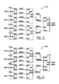
- FIGS. 13-17 are block diagrams of multiple match detection circuits according to embodiments of the present invention.
- a 2-to-1 multiple match gate 101 generates active high output signals in response to active low input signals.
- the multiple match gate 101 receives four active low input signals, which are shown as NAM0 (“not any match zero”), NAM1 (“not any match one”), NMM0 (“not multiple match zero”) and NMM1 (“not multiple match one”).
- the multiple match gate 101 In response to these four active low input signals, the multiple match gate 101 generates an active high “any match flag” (AMF) and an active high “multiple match flag” (MMF).
- AMF active high “any match flag”
- MMF active high “multiple match flag”
- the AMF is generated by a NAND gate, which is shown as NAND_AMF.
- the AMF will be generated as an active high signal whenever either signal NAM0 or NAM1 is active at a low level or both signals are active at low levels.
- the NAND gate NAND_AMF may be defined by four transistors.
- the MMF is generated by a multiple match circuit having four PMOS transistors and four NMOS transistors.
- the multiple match circuit is illustrated as an “input-low output-high” multiple match circuit (MM_ILOH).
- the four transistors within the NAND gate NAND_AMF and the eight transistors within the multiple match circuit MM_ILOH operate in accordance with the truth table illustrated by TABLE 1.
- the sixteen entries within the truth table of TABLE 1 include seven (7) entries that represent an invalid combination of input signals.
- at least one of the active low multiple match signals (NMM0 and/or NMM1) is erroneously indicated as being “true” when a corresponding any match signal (NAM0 and/or NAM1) is indicated as being “false.”
- NMM0 and/or NMM1 the active low multiple match signals
- NAM0 and/or NAM1 corresponding any match signal
- a 2-to-1 multiple match gate 102 generates active low output signals in response to active high input signals.
- the multiple match gate 102 receives four active high input signals, which are shown as AM0 (“any match zero”), AM1 (“any match one”), MM0 (“multiple match zero”) and MM1 (“multiple match one”).
- the multiple match gate 102 generates an active low “not any match flag” (NAMF) and an active low “not multiple match flag” (NMMF).
- NAMF active low “not any match flag”
- NMMF active low “not multiple match flag”
- the NAMF is generated by a NOR gate, which is shown as NOR_NAMF.
- the NAMF will be generated as an active low signal whenever either signal AM0 or AM1 is active at a high level or both signals are active at high levels.
- the NOR gate NOR_NAMF may be defined by four transistors.
- the NMMF is generated by a multiple match circuit having four PMOS transistors and four NMOS transistors.
- the multiple match circuit is illustrated as an “input-high output-low” multiple match circuit (MM_IHOL).
- the four transistors within the NOR gate NOR_NAMF and the eight transistors within the multiple match circuit MM_IHOL operate in accordance with the truth table illustrated by TABLE 2.
- the sixteen entries within the truth table of TABLE 2 include seven (7) entries that represent an invalid combination of input signals.
- at least one of the active high multiple match signals (MM0 and/or MM1) is erroneously indicated as being “true” when a corresponding any match signal (AM0 and/or AM1) is indicated as being “false.”
- it is impossible for MM0 to be true (i.e., MM0 1) when AM0 is false (i.e.
- the multiple match gates 101 and 102 of FIGS. 1 and 2 represent direct implementations of the circuitry needed to meet the boolean expressions set forth in equations (1) and (2).
- the speed of the multiple match gates 101 and 102 illustrated by FIGS. 1-2 may be limited by the presence of three NMOS transistors in the pull-down paths of the multiple match circuit MM_ILOH of FIG. 1 and the presence of three PMOS transistors in the pull-up paths of the multiple match circuit MM_IHOL of FIG. 2 .
- These speed enhancing techniques may also be applied to other multiple match gates, including multiple match gates having a greater input to output signal ratio (e.g., 4-to-1 multiple match gates).
- the 2-to-1 multiple match gates 103 and 104 of FIGS. 3-4 are provided as the basic building blocks of larger multiple match detection circuits having multiple stages.
- the multiple match gate 103 of FIG. 3 includes a multiple match circuit MM_ILOH having only two NMOS transistors in a worst case pull-down path and the multiple match gate 104 of FIG. 4 includes a multiple match circuit MM_IHOL having only two PMOS transistors in a worst case pull-up path.
- the reduction in the number of NMOS transistors in the worst case pull-down path is made possible because the output of the pull-down network, MMF, will only be low (false) when either a no match or only a single match is present.
- MMF pull-down network
- the multiple match circuit MM_ILOH of FIG. 3 is a boolean equivalent to the multiple match circuit MM_ILOH of FIG. 1 for valid combinations of inputs, but has better worst case speed performance.
- the multiple match circuit MM_ILOH within the multiple match gate 103 of FIG. 3 may be defined as having multiple pull-down and pull-up paths.
- the multiple match circuit MM_ILOH includes two pull-down paths and three pull-up paths that stem from the output terminal MMF.
- the first pull-down path is defined by a series combination of a first NMOS transistor N 1 having a gate terminal that is configured to receive the not any match signal NAM0 and a second NMOS transistor N 2 having a gate terminal that is configured to receive the not multiple match signal NMM1.
- the second pull-down path is defined by a series combination of a third NMOS transistor N 3 having a gate terminal that is configured to receive the not any match signal NAM1 and a fourth NMOS transistor N 4 having a gate terminal that is configured to receive the not multiple match signal NMM0.
- the first pull-up path is defined by a first PMOS transistor P 1 that is configured to receive the not multiple match signal NMM0
- the second pull-up path is defined by a second PMOS transistor P 2 that is configured to receive the not multiple match signal NMM1.
- the third pull-up path is defined by a series combination of a third PMOS transistor P 3 having a gate terminal that is configured to receive the not any match signal NAM0 and a fourth PMOS transistor P 4 having a gate terminal that is configured to receive the not any match signal NAM1.
- the reduction in the number of PMOS transistors in the worst case pull-up path is made possible because the output of the pull-up network, NMMF, will only be high (false) when either a no match or only a single match is present.
- NMMF NOT (( MM 0 +AM 1) ⁇ ( AM 0 +MM 1)) (4)
- the multiple match circuit MM_IHOL of FIG. 4 is a boolean equivalent to the multiple match circuit MM_IHOL of FIG. 2 for valid combinations of inputs, but has better worst case speed performance.
- the multiple match circuit MM_IHOL within the multiple match gate 104 of FIG. 4 may be defined as having multiple pull-down and pull-up paths.
- the multiple match circuit MM_IHOL includes two pull-up paths and three pull-down paths that stem from the output terminal NMMF.
- the first pull-up path is defined by a series combination of a first PMOS transistor P 1 having a gate terminal that is configured to receive the any match signal AM0 and a second PMOS transistor P 2 having a gate terminal that is configured to receive the multiple match signal MM1.
- the second pull-up path is defined by a series combination of a third PMOS transistor P 3 having a gate terminal that is configured to receive the any match signal AM1 and a fourth PMOS transistor P 4 having a gate terminal that is configured to receive the multiple match signal MM0.
- the first pull-down path is defined by a first NMOS transistor N 1 that is configured to receive the multiple match signal MM0
- the second pull-down path is defined by a second NMOS transistor N 2 that is configured to receive the multiple match signal MM1.
- the third pull-down path is defined by a series combination of a third NMOS transistor N 3 having a gate terminal that is configured to receive the any match signal AM0 and a fourth NMOS transistor N 4 having a gate terminal that is configured to receive the any match signal AM1.
- the multiple match gate 103 of FIG. 3 can be further simplified when it is used in a first stage of a multiple match detection circuit that is configured to receive not any match signals (NAM0, NAM1, . . . ). This is typically the case when the first stage of the multiple match detection circuit is configured to receive active low match signals from a CAM array (or multiple CAM array devices). In this case, the not multiple match signal lines NMM0 and NMM1 may not exist as inputs. As illustrated by the multiple match gate 107 of FIG.
- the multiple match gate 107 of FIG. 7 may be simplified as shown by the multiple match gate 105 of FIG. 5 , which includes one two-input NAND gate NAND_AMF and one two-input NOR gate NOR_MMF.
- the multiple match gate 108 of FIG. 8 may be simplified as shown by the multiple match gate 106 of FIG. 6 , which includes one two-input NAND gate NAND_NMMF and one two-input NOR gate NOR_NAMF.
- the multiple match gate 109 is shown as being similar to the multiple match gate 103 of FIG. 3 ; however, a pair of inverters INV_NMMF and INV_NAMF have been added to make the number of inversions from input to output even. Each inverter adds two transistors. Thus, the multiple match gate 109 of FIG. 9 is defined by sixteen (16) transistors. Similarly, the multiple match gate 1011 of FIG. 11 is similar to the multiple match gate 105 of FIG. 5 , however, a pair of inverters INV_NMMF and INV_NAMF have been added to make the number of inversions from input to output even. In FIG.
- the multiple match gate 1010 is shown as being similar to the multiple match gate 104 of FIG. 4 , however, a pair of inverters INV_MMF and INV_AMF have been added to make the number of inversions from input to output even.
- the multiple match gate 1012 of FIG. 12 is similar to the multiple match gate 106 of FIG. 6 , however, a pair of inverters INV_MMF and INV_AMF have been added to make the number of inversions from input to output even.
- the above-described 2-to-1 multiple match gates may be used as building blocks to construct multi-stage multiple match detection circuits that are hierarchically cascadable.
- the multiple match detection circuits 1013 - 1017 of FIGS. 13-17 are configured to generate a final multiple match flag (MMF) and a final any match flag (AMF) in response to input match signals that see relatively small fanout.
- MMF final multiple match flag
- AMF final any match flag
- the final MMF is set to an active level whenever at least two of the input match signals indicate a match condition and the AMF is set to an active level whenever at least one of the input match signals indicates a match condition.
- the multiple match detection circuit 1013 is configured to generate a final any match flag AMF07 and a final multiple match flag MMF07 in response to eight (8) match signals [AM0:AM7], which are received at a first stage of the multiple match detection circuit 1013 .
- This first stage of the multiple match detection circuit 1013 includes four multiple match gates, which are configured in accordance with the multiple match gate 1012 of FIG. 12 .
- the intermediate stage of the multiple match detection circuit 1013 includes two multiple match gates, which are configured in accordance with the multiple match gate 1010 of FIG. 10 . These two multiple match gates receive the any match and multiple match flags AMF01-AMF67 and MMF01-MMF67.
- the final stage of the multiple match detection circuit 1013 includes a single multiple match gate 1010 , which receives a pair of any match flags AMF03 and AMF47 and a pair of multiple match flags MMF03 and MMF47.
- the multiple match detection circuit 1013 of FIG. 13 can process eight match signals. These match signals may be generated by respective rows of a CAM array block, by respective CAM array blocks within a CAM device or by respective CAM devices within a multi-chip system, for example.
- the multiple match detection circuit 1014 of FIG. 14 is similar to the multiple match detection circuit 1013 of FIG. 13 , however, the multiple match gates 104 and 103 are used to construct the two intermediate stages and the final stage, respectively. As illustrated, the multiple match gates 104 in the intermediate stage generate not any match flags NAMF03 and NAMF47 and not multiple match flags NMMF03 and NMMF47.
- a three stage multiple match detection circuit 1015 is illustrated as including six multiple match gates 106 , which define a first stage, two multiple match gates 103 , which define an intermediate stage, and a multiple match gate 1010 , which defines a final stage.
- the multiple match gates 106 generate the not any match flags NAMF01, NAMF23, NAMF45 and NAMF67 and the not multiple match flags NMMF01, NMMF23, NMMF45 and NMMF67.
- the two multiple match gates 103 generate the any match flags AMF03 and AMF47 and the multiple match flags MMF03 and MMF47.
- a multiple match detection circuit 1016 which includes seven equivalent multiple match gates 1010 , is illustrated.
- the four multiple match gates 1010 associated with the first stage include multiple match inputs MM0 and MM1 that are tied to ground, to thereby represent false conditions.
- the two multiple match gates 1010 associated with the intermediate stage generate the any match flags AMF03 and AMF47 and the multiple match flags MMF03 and MMF47.
- the multiple match gate 1010 associated with the final stage generates the final any match flag AMF07 and the final multiple match flag MMF07.
- FIG. 17 illustrates a four-stage multiple match detection circuit 1017 that is configured to process sixteen (16) match signals, which are shown as AM[0:151].
- the first stage of the multiple match detection circuit 1017 includes eight input-high output-low (IHOL) multiple match gates 106 and the second stage includes four input-low output-high (ILOH) multiple match gates 103 .
- the third stage of the multiple match detection circuit 1017 includes two input-high output-low (IHOL) multiple match gates 104 and the fourth and final stage includes another copy of the input-low output-high; (ILOH) multiple match gate 103 .
- IHOL input-high output-low
- ILOH input-low output-high
- the 17 includes a plurality of stages of multiple match gates (e.g., second, third and fourth stages) that are each configured to generate a respective pair of any match and multiple match flags.
- the plurality of stages include at least two stages that are arranged in an alternating input-high output-low (IHOL) and input-low output-high (ILOH) sequence.
- the multiple match gates in the final and intermediate stages may be configured with only twelve (12) transistors per gate and the multiple match gates in the first stage may be configured with only eight (8) transistors per gate.
- a multiple match detection-circuit can be configured so that each of the N match signals sees a relatively small fanout to the gate terminals of only four MOS transistors.
Abstract
Description
| TABLE 1 | |||||||
| NAM0 | NMM0 | NAM1 | NMM1 | | MMF | DESCRIPTION | |
| 0 | 0 | 0 | 0 | 1 | 1 | |
|
| 0 | 0 | 0 | 1 | 1 | 1 | |
|
| 0 | 0 | 1 | 0 | X | X | |
|
| 0 | 0 | 1 | 1 | 1 | 1 | |
|
| 0 | 1 | 0 | 0 | 1 | 1 | |
|
| 0 | 1 | 0 | 1 | 1 | 1 | |
|
| 0 | 1 | 1 | 0 | X | X | |
|
| 0 | 1 | 1 | 1 | 1 | 0 | |
|
| 1 | 0 | 0 | 0 | X | X | |
|
| 1 | 0 | 0 | 1 | X | X | |
|
| 1 | 0 | 1 | 0 | X | X | |
|
| 1 | 0 | 1 | 1 | X | X | |
|
| 1 | 1 | 0 | 0 | 1 | 1 | |
|
| 1 | 1 | 0 | 1 | 1 | 0 | |
|
| 1 | 1 | 1 | 0 | X | X | |
|
| 1 | 1 | 1 | 1 | 0 | 0 | No Match | |
MMF=NOT(NMM0×NMM1(NAM0+NAM1)) (1)
| TABLE 2 | |||||||
| AM0 | MM0 | AM1 | MM1 | | NMMF | DESCRIPTION | |
| 0 | 0 | 0 | 0 | 1 | 1 | No |
|
| 0 | 0 | 0 | 1 | X | X | |
|
| 0 | 0 | 1 | 0 | 0 | 1 | |
|
| 0 | 0 | 1 | 1 | 0 | 0 | |
|
| 0 | 1 | 0 | 0 | X | X | |
|
| 0 | 1 | 0 | 1 | X | X | |
|
| 0 | 1 | 1 | 0 | X | X | |
|
| 0 | 1 | 1 | 1 | X | X | |
|
| 1 | 0 | 0 | 0 | 0 | 1 | |
|
| 1 | 0 | 0 | 1 | X | X | |
|
| 1 | 0 | 1 | 0 | 0 | 0 | |
|
| 1 | 0 | 1 | 1 | 0 | 0 | |
|
| 1 | 1 | 0 | 0 | 0 | 0 | |
|
| 1 | 1 | 0 | 1 | X | X | |
|
| 1 | 1 | 1 | 0 | 0 | 0 | |
|
| 1 | 1 | 1 | 1 | 0 | 0 | Multiple Match | |
NMMF=NOT(MMF)=NOT(MM0+MM1+(AM0×AM1)) (2)
MMF=NOT((NMM0×NAM1)+(NAM0×NMM1)) (3)
Thus, the multiple match circuit MM_ILOH of
NMMF=NOT((MM0+AM1)×(AM0+MM1)) (4)
Thus, the multiple match circuit MM_IHOL of
148=(8 transistors/gate)(8 first stage gates 106)+(12 transistors/gate)(4 second stage gates 103)+(12 transistors/gate)(2 third stage gates 104)+(12 transistors/gate)(1 final stage gate 103)=((½N×8)+((½N−1)×12)), where N=16.
Claims (4)
MMF=NOT((NMM0×NAM1)+(NAM0×NMM1)).
NMMF=NOT((MM0+AM1)×(AM0+MM1)).
Priority Applications (1)
| Application Number | Priority Date | Filing Date | Title |
|---|---|---|---|
| US10/869,387 US6859378B1 (en) | 2003-03-10 | 2004-06-16 | Multiple match detection logic and gates for content addressable memory (CAM) devices |
Applications Claiming Priority (2)
| Application Number | Priority Date | Filing Date | Title |
|---|---|---|---|
| US10/385,155 US6924994B1 (en) | 2003-03-10 | 2003-03-10 | Content addressable memory (CAM) devices having scalable multiple match detection circuits therein |
| US10/869,387 US6859378B1 (en) | 2003-03-10 | 2004-06-16 | Multiple match detection logic and gates for content addressable memory (CAM) devices |
Related Parent Applications (1)
| Application Number | Title | Priority Date | Filing Date |
|---|---|---|---|
| US10/385,155 Division US6924994B1 (en) | 2003-03-10 | 2003-03-10 | Content addressable memory (CAM) devices having scalable multiple match detection circuits therein |
Publications (1)
| Publication Number | Publication Date |
|---|---|
| US6859378B1 true US6859378B1 (en) | 2005-02-22 |
Family
ID=34134976
Family Applications (2)
| Application Number | Title | Priority Date | Filing Date |
|---|---|---|---|
| US10/385,155 Expired - Fee Related US6924994B1 (en) | 2003-03-10 | 2003-03-10 | Content addressable memory (CAM) devices having scalable multiple match detection circuits therein |
| US10/869,387 Expired - Fee Related US6859378B1 (en) | 2003-03-10 | 2004-06-16 | Multiple match detection logic and gates for content addressable memory (CAM) devices |
Family Applications Before (1)
| Application Number | Title | Priority Date | Filing Date |
|---|---|---|---|
| US10/385,155 Expired - Fee Related US6924994B1 (en) | 2003-03-10 | 2003-03-10 | Content addressable memory (CAM) devices having scalable multiple match detection circuits therein |
Country Status (1)
| Country | Link |
|---|---|
| US (2) | US6924994B1 (en) |
Cited By (6)
| Publication number | Priority date | Publication date | Assignee | Title |
|---|---|---|---|---|
| US7185141B1 (en) * | 2001-12-27 | 2007-02-27 | Netlogic Microsystems, Inc. | Apparatus and method for associating information values with portions of a content addressable memory (CAM) device |
| US20090034311A1 (en) * | 2007-08-01 | 2009-02-05 | Texas Instruments Incorporated | Low power ternary content-addressable memory (tcam) |
| US7822916B1 (en) | 2006-10-31 | 2010-10-26 | Netlogic Microsystems, Inc. | Integrated circuit search engine devices having priority sequencer circuits therein that sequentially encode multiple match signals |
| US8073005B1 (en) | 2001-12-27 | 2011-12-06 | Cypress Semiconductor Corporation | Method and apparatus for configuring signal lines according to idle codes |
| US9063840B1 (en) | 2009-08-21 | 2015-06-23 | Broadcom Corporation | Multiple match detection for multiple flows in a content addressable memory |
| US20160358654A1 (en) * | 2015-06-02 | 2016-12-08 | Cisco Technology, Inc. | Low-power ternary content addressable memory |
Families Citing this family (1)
| Publication number | Priority date | Publication date | Assignee | Title |
|---|---|---|---|---|
| US7363423B2 (en) * | 2004-08-02 | 2008-04-22 | Lsi Logic Corporation | Multiple match detection circuit |
Citations (24)
| Publication number | Priority date | Publication date | Assignee | Title |
|---|---|---|---|---|
| US5748070A (en) | 1995-09-13 | 1998-05-05 | Lsi Logic Corporation | High speed method and apparatus for detecting assertion of multiple signals |
| US5852569A (en) | 1997-05-20 | 1998-12-22 | Quality Semiconductor, Inc. | Content addressable memory multiple match detection circuit |
| US6044005A (en) | 1999-02-03 | 2000-03-28 | Sibercore Technologies Incorporated | Content addressable memory storage device |
| US6137707A (en) | 1999-03-26 | 2000-10-24 | Netlogic Microsystems | Method and apparatus for simultaneously performing a plurality of compare operations in content addressable memory device |
| US6175513B1 (en) | 1999-07-12 | 2001-01-16 | Netlogic Microsystems | Method and apparatus for detecting multiple matches in a content addressable memory |
| US6175514B1 (en) | 1999-01-15 | 2001-01-16 | Fast-Chip, Inc. | Content addressable memory device |
| US6195277B1 (en) | 1999-09-13 | 2001-02-27 | Lara Technology, Inc. | Multiple signal detection circuit |
| US6243281B1 (en) | 2000-06-14 | 2001-06-05 | Netlogic Microsystems, Inc. | Method and apparatus for accessing a segment of CAM cells in an intra-row configurable CAM system |
| US6301636B1 (en) | 1997-08-28 | 2001-10-09 | Nortel Networks Limited | Content addressable memory system with cascaded memories and self timed signals |
| US6307798B1 (en) | 1999-07-12 | 2001-10-23 | Mosaid Technologies Incorporated | Circuit and method for multiple match detection in content addressable memories |
| US6317350B1 (en) | 2000-06-16 | 2001-11-13 | Netlogic Microsystems, Inc. | Hierarchical depth cascading of content addressable memory devices |
| US6392910B1 (en) | 1999-09-10 | 2002-05-21 | Sibercore Technologies, Inc. | Priority encoder with multiple match function for content addressable memories and methods for implementing the same |
| US6480406B1 (en) * | 2001-08-22 | 2002-11-12 | Cypress Semiconductor Corp. | Content addressable memory cell |
| US6490650B1 (en) | 2000-12-08 | 2002-12-03 | Netlogic Microsystems, Inc. | Method and apparatus for generating a device index in a content addressable memory |
| US6493793B1 (en) | 2000-06-16 | 2002-12-10 | Netlogic Microsystems, Inc. | Content addressable memory device having selective cascade logic and method for selectively combining match information in a CAM device |
| US6499081B1 (en) | 1999-02-23 | 2002-12-24 | Netlogic Microsystems, Inc. | Method and apparatus for determining a longest prefix match in a segmented content addressable memory device |
| US20030005146A1 (en) | 2001-06-18 | 2003-01-02 | Integrated Device Technology, Inc. | Content addressable memory array having flexible priority support |
| US20030145178A1 (en) | 2002-01-31 | 2003-07-31 | Charles Jiang | Circuit and method for detecting multiple matches in a content addressable memory |
| US20040015652A1 (en) | 2002-07-22 | 2004-01-22 | Kee Park | Multi-bank content addressable memory (CAM) devices having staged segment-to-segment soft and hard priority resolution circuits therein and methods of operating same |
| US6687785B1 (en) | 2000-06-08 | 2004-02-03 | Netlogic Microsystems, Inc. | Method and apparatus for re-assigning priority in a partitioned content addressable memory device |
| US6697912B2 (en) | 1999-12-20 | 2004-02-24 | Intel Corporation | Prioritized content addressable memory |
| US6707694B2 (en) | 2001-07-06 | 2004-03-16 | Micron Technology, Inc. | Multi-match detection circuit for use with content-addressable memories |
| US6717876B2 (en) | 2001-12-28 | 2004-04-06 | Mosaid Technologies Incorporated | Matchline sensing for content addressable memories |
| US6728124B1 (en) | 2001-08-03 | 2004-04-27 | Netlogic Microsystems, Inc. | Content addressable memory with error detection signaling |
Family Cites Families (4)
| Publication number | Priority date | Publication date | Assignee | Title |
|---|---|---|---|---|
| IT1308100B1 (en) * | 1999-05-17 | 2001-11-29 | Cselt Centro Studi Lab Telecom | REFERENCES TO ADDRESSABLE MEMORIES THROUGH THE CONTENT |
| US6288922B1 (en) * | 2000-08-11 | 2001-09-11 | Silicon Access Networks, Inc. | Structure and method of an encoded ternary content addressable memory (CAM) cell for low-power compare operation |
| US6577519B1 (en) * | 2001-08-30 | 2003-06-10 | Sibercore Technologies, Inc. | System and method for low power searching in content addressable memories using sample search words |
| CA2365891C (en) * | 2001-10-31 | 2012-03-13 | Mosaid Technologies Incorporated | Priority encoder circuit and method for content addressable memory |
-
2003
- 2003-03-10 US US10/385,155 patent/US6924994B1/en not_active Expired - Fee Related
-
2004
- 2004-06-16 US US10/869,387 patent/US6859378B1/en not_active Expired - Fee Related
Patent Citations (26)
| Publication number | Priority date | Publication date | Assignee | Title |
|---|---|---|---|---|
| US5748070A (en) | 1995-09-13 | 1998-05-05 | Lsi Logic Corporation | High speed method and apparatus for detecting assertion of multiple signals |
| US5852569A (en) | 1997-05-20 | 1998-12-22 | Quality Semiconductor, Inc. | Content addressable memory multiple match detection circuit |
| US6301636B1 (en) | 1997-08-28 | 2001-10-09 | Nortel Networks Limited | Content addressable memory system with cascaded memories and self timed signals |
| US6362993B1 (en) * | 1999-01-15 | 2002-03-26 | Fast-Chip Incorporated | Content addressable memory device |
| US6175514B1 (en) | 1999-01-15 | 2001-01-16 | Fast-Chip, Inc. | Content addressable memory device |
| US6044005A (en) | 1999-02-03 | 2000-03-28 | Sibercore Technologies Incorporated | Content addressable memory storage device |
| US6499081B1 (en) | 1999-02-23 | 2002-12-24 | Netlogic Microsystems, Inc. | Method and apparatus for determining a longest prefix match in a segmented content addressable memory device |
| US6137707A (en) | 1999-03-26 | 2000-10-24 | Netlogic Microsystems | Method and apparatus for simultaneously performing a plurality of compare operations in content addressable memory device |
| US6175513B1 (en) | 1999-07-12 | 2001-01-16 | Netlogic Microsystems | Method and apparatus for detecting multiple matches in a content addressable memory |
| US6307798B1 (en) | 1999-07-12 | 2001-10-23 | Mosaid Technologies Incorporated | Circuit and method for multiple match detection in content addressable memories |
| US6392910B1 (en) | 1999-09-10 | 2002-05-21 | Sibercore Technologies, Inc. | Priority encoder with multiple match function for content addressable memories and methods for implementing the same |
| US6195277B1 (en) | 1999-09-13 | 2001-02-27 | Lara Technology, Inc. | Multiple signal detection circuit |
| US6697912B2 (en) | 1999-12-20 | 2004-02-24 | Intel Corporation | Prioritized content addressable memory |
| US6687785B1 (en) | 2000-06-08 | 2004-02-03 | Netlogic Microsystems, Inc. | Method and apparatus for re-assigning priority in a partitioned content addressable memory device |
| US6243281B1 (en) | 2000-06-14 | 2001-06-05 | Netlogic Microsystems, Inc. | Method and apparatus for accessing a segment of CAM cells in an intra-row configurable CAM system |
| US6493793B1 (en) | 2000-06-16 | 2002-12-10 | Netlogic Microsystems, Inc. | Content addressable memory device having selective cascade logic and method for selectively combining match information in a CAM device |
| US6317350B1 (en) | 2000-06-16 | 2001-11-13 | Netlogic Microsystems, Inc. | Hierarchical depth cascading of content addressable memory devices |
| US6490650B1 (en) | 2000-12-08 | 2002-12-03 | Netlogic Microsystems, Inc. | Method and apparatus for generating a device index in a content addressable memory |
| US6718433B1 (en) | 2000-12-08 | 2004-04-06 | Netlogic Microsystems, Inc. | Match and priority encoding logic circuit |
| US20030005146A1 (en) | 2001-06-18 | 2003-01-02 | Integrated Device Technology, Inc. | Content addressable memory array having flexible priority support |
| US6707694B2 (en) | 2001-07-06 | 2004-03-16 | Micron Technology, Inc. | Multi-match detection circuit for use with content-addressable memories |
| US6728124B1 (en) | 2001-08-03 | 2004-04-27 | Netlogic Microsystems, Inc. | Content addressable memory with error detection signaling |
| US6480406B1 (en) * | 2001-08-22 | 2002-11-12 | Cypress Semiconductor Corp. | Content addressable memory cell |
| US6717876B2 (en) | 2001-12-28 | 2004-04-06 | Mosaid Technologies Incorporated | Matchline sensing for content addressable memories |
| US20030145178A1 (en) | 2002-01-31 | 2003-07-31 | Charles Jiang | Circuit and method for detecting multiple matches in a content addressable memory |
| US20040015652A1 (en) | 2002-07-22 | 2004-01-22 | Kee Park | Multi-bank content addressable memory (CAM) devices having staged segment-to-segment soft and hard priority resolution circuits therein and methods of operating same |
Non-Patent Citations (1)
| Title |
|---|
| Miller et al., "Content Addressable Memory Array Having Flexible Priority Support," U.S. Appl. No. 09/884,797, filed Jun. 18, 2001. |
Cited By (8)
| Publication number | Priority date | Publication date | Assignee | Title |
|---|---|---|---|---|
| US7185141B1 (en) * | 2001-12-27 | 2007-02-27 | Netlogic Microsystems, Inc. | Apparatus and method for associating information values with portions of a content addressable memory (CAM) device |
| US8073005B1 (en) | 2001-12-27 | 2011-12-06 | Cypress Semiconductor Corporation | Method and apparatus for configuring signal lines according to idle codes |
| US7822916B1 (en) | 2006-10-31 | 2010-10-26 | Netlogic Microsystems, Inc. | Integrated circuit search engine devices having priority sequencer circuits therein that sequentially encode multiple match signals |
| US20090034311A1 (en) * | 2007-08-01 | 2009-02-05 | Texas Instruments Incorporated | Low power ternary content-addressable memory (tcam) |
| WO2009032457A1 (en) * | 2007-08-01 | 2009-03-12 | Texas Instruments Incorporated | Low power ternary content-addressable memory (tcam) |
| US8125810B2 (en) | 2007-08-01 | 2012-02-28 | Texas Instruments Incorporated | Low power ternary content-addressable memory (TCAM) |
| US9063840B1 (en) | 2009-08-21 | 2015-06-23 | Broadcom Corporation | Multiple match detection for multiple flows in a content addressable memory |
| US20160358654A1 (en) * | 2015-06-02 | 2016-12-08 | Cisco Technology, Inc. | Low-power ternary content addressable memory |
Also Published As
| Publication number | Publication date |
|---|---|
| US6924994B1 (en) | 2005-08-02 |
Similar Documents
| Publication | Publication Date | Title |
|---|---|---|
| US6499081B1 (en) | Method and apparatus for determining a longest prefix match in a segmented content addressable memory device | |
| US6460112B1 (en) | Method and apparatus for determining a longest prefix match in a content addressable memory device | |
| US6944709B2 (en) | Content addressable memory with block-programmable mask write mode, word width and priority | |
| US6266262B1 (en) | Enhanced binary content addressable memory for longest prefix address matching | |
| US7246198B2 (en) | Content addressable memory with programmable word width and programmable priority | |
| US6757779B1 (en) | Content addressable memory with selectable mask write mode | |
| US6253280B1 (en) | Programmable multiple word width CAM architecture | |
| US6539455B1 (en) | Method and apparatus for determining an exact match in a ternary content addressable memory device | |
| US7417881B2 (en) | Low power content addressable memory | |
| US6574702B2 (en) | Method and apparatus for determining an exact match in a content addressable memory device | |
| US7110275B2 (en) | High speed NAND-type content addressable memory (CAM) | |
| US6564289B2 (en) | Method and apparatus for performing a read next highest priority match instruction in a content addressable memory device | |
| US6804744B1 (en) | Content addressable memory having sections with independently configurable entry widths | |
| US20060280193A1 (en) | Method and apparatus for performing packet classification for policy-based packet routing | |
| JPS58212698A (en) | Storage device | |
| US7355890B1 (en) | Content addressable memory (CAM) devices having NAND-type compare circuits | |
| US8059440B2 (en) | Content-addressable memory | |
| US6420990B1 (en) | Priority selection circuit | |
| US6859378B1 (en) | Multiple match detection logic and gates for content addressable memory (CAM) devices | |
| US20020105821A1 (en) | Relational content addressable memory | |
| US7095641B1 (en) | Content addressable memory (CAM) devices having priority class detectors therein that perform local encoding of match line signals | |
| US7206212B1 (en) | Content addressable memory (CAM) device with entries having ternary match and range compare functions | |
| US6618280B2 (en) | Associative memory for accomplishing longest coincidence data detection by two comparing operations | |
| US6718433B1 (en) | Match and priority encoding logic circuit | |
| US7889530B2 (en) | Reconfigurable content-addressable memory |
Legal Events
| Date | Code | Title | Description |
|---|---|---|---|
| CC | Certificate of correction | ||
| FPAY | Fee payment |
Year of fee payment: 4 |
|
| REMI | Maintenance fee reminder mailed | ||
| AS | Assignment |
Owner name: SILICON VALLEY BANK, CALIFORNIA Free format text: SECURITY AGREEMENT;ASSIGNORS:NETLOGIC MICROSYSTEMS, INC.;NETLOGIC MICROSYSTEMS INTERNATIONAL LIMITED;NETLOGIC MICROSYSTEMS CAYMANS LIMITED;REEL/FRAME:022973/0710 Effective date: 20090717 Owner name: SILICON VALLEY BANK,CALIFORNIA Free format text: SECURITY AGREEMENT;ASSIGNORS:NETLOGIC MICROSYSTEMS, INC.;NETLOGIC MICROSYSTEMS INTERNATIONAL LIMITED;NETLOGIC MICROSYSTEMS CAYMANS LIMITED;REEL/FRAME:022973/0710 Effective date: 20090717 |
|
| AS | Assignment |
Owner name: NETLOGIC MICROSYSTEMS, INC., CALIFORNIA Free format text: ASSIGNMENT OF ASSIGNORS INTEREST;ASSIGNOR:INTEGRATED DEVICE TECHNOLOGY, INC.;REEL/FRAME:022980/0624 Effective date: 20090717 |
|
| FEPP | Fee payment procedure |
Free format text: PAYOR NUMBER ASSIGNED (ORIGINAL EVENT CODE: ASPN); ENTITY STATUS OF PATENT OWNER: LARGE ENTITY Free format text: PAYER NUMBER DE-ASSIGNED (ORIGINAL EVENT CODE: RMPN); ENTITY STATUS OF PATENT OWNER: LARGE ENTITY |
|
| AS | Assignment |
Owner name: NETLOGIC MICROSYSTEMS, INC., CALIFORNIA Free format text: RELEASE BY SECURED PARTY;ASSIGNOR:SILICON VALLEY BANK;REEL/FRAME:026830/0141 Effective date: 20110826 Owner name: NETLOGIC MICROSYSTEMS INTERNATIONAL LIMITED, CALIF Free format text: RELEASE BY SECURED PARTY;ASSIGNOR:SILICON VALLEY BANK;REEL/FRAME:026830/0141 Effective date: 20110826 Owner name: NETLOGIC MICROSYSTEMS CAYMANS LIMITED, CALIFORNIA Free format text: RELEASE BY SECURED PARTY;ASSIGNOR:SILICON VALLEY BANK;REEL/FRAME:026830/0141 Effective date: 20110826 |
|
| REMI | Maintenance fee reminder mailed | ||
| LAPS | Lapse for failure to pay maintenance fees | ||
| STCH | Information on status: patent discontinuation |
Free format text: PATENT EXPIRED DUE TO NONPAYMENT OF MAINTENANCE FEES UNDER 37 CFR 1.362 |
|
| FP | Lapsed due to failure to pay maintenance fee |
Effective date: 20130222 |
|
| AS | Assignment |
Owner name: NETLOGIC I LLC, DELAWARE Free format text: CHANGE OF NAME;ASSIGNOR:NETLOGIC MICROSYSTEMS, INC.;REEL/FRAME:035443/0824 Effective date: 20130123 Owner name: BROADCOM CORPORATION, CALIFORNIA Free format text: ASSIGNMENT OF ASSIGNORS INTEREST;ASSIGNOR:NETLOGIC I LLC;REEL/FRAME:035443/0763 Effective date: 20150327 |
|
| AS | Assignment |
Owner name: BANK OF AMERICA, N.A., AS COLLATERAL AGENT, NORTH CAROLINA Free format text: PATENT SECURITY AGREEMENT;ASSIGNOR:BROADCOM CORPORATION;REEL/FRAME:037806/0001 Effective date: 20160201 Owner name: BANK OF AMERICA, N.A., AS COLLATERAL AGENT, NORTH Free format text: PATENT SECURITY AGREEMENT;ASSIGNOR:BROADCOM CORPORATION;REEL/FRAME:037806/0001 Effective date: 20160201 |
|
| AS | Assignment |
Owner name: AVAGO TECHNOLOGIES GENERAL IP (SINGAPORE) PTE. LTD., SINGAPORE Free format text: ASSIGNMENT OF ASSIGNORS INTEREST;ASSIGNOR:BROADCOM CORPORATION;REEL/FRAME:041706/0001 Effective date: 20170120 Owner name: AVAGO TECHNOLOGIES GENERAL IP (SINGAPORE) PTE. LTD Free format text: ASSIGNMENT OF ASSIGNORS INTEREST;ASSIGNOR:BROADCOM CORPORATION;REEL/FRAME:041706/0001 Effective date: 20170120 |
|
| AS | Assignment |
Owner name: BROADCOM CORPORATION, CALIFORNIA Free format text: TERMINATION AND RELEASE OF SECURITY INTEREST IN PATENTS;ASSIGNOR:BANK OF AMERICA, N.A., AS COLLATERAL AGENT;REEL/FRAME:041712/0001 Effective date: 20170119 |