US6876226B2 - Integrated digital circuit - Google Patents
Integrated digital circuit Download PDFInfo
- Publication number
- US6876226B2 US6876226B2 US10/372,721 US37272103A US6876226B2 US 6876226 B2 US6876226 B2 US 6876226B2 US 37272103 A US37272103 A US 37272103A US 6876226 B2 US6876226 B2 US 6876226B2
- Authority
- US
- United States
- Prior art keywords
- volatile storage
- storage component
- circuit portion
- logic
- logic circuit
- Prior art date
- Legal status (The legal status is an assumption and is not a legal conclusion. Google has not performed a legal analysis and makes no representation as to the accuracy of the status listed.)
- Expired - Lifetime
Links
Images


Classifications
-
- H—ELECTRICITY
- H03—ELECTRONIC CIRCUITRY
- H03K—PULSE TECHNIQUE
- H03K19/00—Logic circuits, i.e. having at least two inputs acting on one output; Inverting circuits
- H03K19/02—Logic circuits, i.e. having at least two inputs acting on one output; Inverting circuits using specified components
- H03K19/173—Logic circuits, i.e. having at least two inputs acting on one output; Inverting circuits using specified components using elementary logic circuits as components
-
- G—PHYSICS
- G11—INFORMATION STORAGE
- G11C—STATIC STORES
- G11C11/00—Digital stores characterised by the use of particular electric or magnetic storage elements; Storage elements therefor
- G11C11/21—Digital stores characterised by the use of particular electric or magnetic storage elements; Storage elements therefor using electric elements
- G11C11/22—Digital stores characterised by the use of particular electric or magnetic storage elements; Storage elements therefor using electric elements using ferroelectric elements
-
- H—ELECTRICITY
- H03—ELECTRONIC CIRCUITRY
- H03K—PULSE TECHNIQUE
- H03K3/00—Circuits for generating electric pulses; Monostable, bistable or multistable circuits
- H03K3/02—Generators characterised by the type of circuit or by the means used for producing pulses
- H03K3/353—Generators characterised by the type of circuit or by the means used for producing pulses by the use, as active elements, of field-effect transistors with internal or external positive feedback
- H03K3/356—Bistable circuits
-
- G—PHYSICS
- G11—INFORMATION STORAGE
- G11C—STATIC STORES
- G11C13/00—Digital stores characterised by the use of storage elements not covered by groups G11C11/00, G11C23/00, or G11C25/00
- G11C13/0002—Digital stores characterised by the use of storage elements not covered by groups G11C11/00, G11C23/00, or G11C25/00 using resistive RAM [RRAM] elements
- G11C13/0004—Digital stores characterised by the use of storage elements not covered by groups G11C11/00, G11C23/00, or G11C25/00 using resistive RAM [RRAM] elements comprising amorphous/crystalline phase transition cells
Definitions
- the invention relates to the field of digital design in microelectronics. More specifically, the invention relates to an integrated digital circuit comprising a logic circuit portion which takes one of at least two different logic states in accordance with provided control signals. The invention relates equally to a device comprising such an integrated digital circuit and to a method of operating such a digital circuit.
- Integrated digital circuits comprising logic circuit portions which are able to take one of at least two different logic states are well known from the state of the art, e.g. in form of conventional static complementary metal-oxide semiconductor (SCMOS) circuits.
- SCMOS static complementary metal-oxide semiconductor
- the status of such a logic circuit portion can be represented for example by flip-flops and latches realized by means of CMOS transistors.
- FIG. 1 shows a conventional CMOS latch, which is part of a digital circuit and which is able to take one of two different logic states.
- the CMOS latch of FIG. 1 comprises two p-channel enhancement MOSFETs (metal-oxide semiconductor field-effect transistors) T 11 , T 13 and two n-channel enhancement MOSFETs T 12 , T 14 .
- the source of the first p-channel MOSFET T 11 is connected to a power supply Vdd.
- the drain of the first p-channel MOSFET T 11 is connected to the drain of the first n-channel MOSFET T 12 .
- the source of the first n-channel MOSFET T 12 is connected to ground Gnd.
- the second p-channel MOSFET T 13 and the second n-channel MOSFET T 14 are arranged in exactly the same way between the power supply Vdd and ground Gnd.
- the gate of the first p-channel MOSFET T 11 and the gate of the first n-channel MOSFET T 12 are connected on the one hand to a clocked input “in” and on the other hand to the connection between the second p-channel MOSFET T 13 and the second n-channel MOSFET T 14 .
- the clocking is represented in FIG. 1 by a switch clk.
- the connection between the first p-channel MOSFET T 11 and the first n-channel MOSFET T 12 is connected on the one hand to an output “out” of the CMOS latch and on the other hand to the gate of the second p-channel MOSFET T 13 and the gate of the second n-channel MOSFET T 14 .
- the first p-channel MOSFET T 11 When a low input voltage is provided to the input “in” of the CMOS latch, the first p-channel MOSFET T 11 is conducting while the first n-channel MOSFET T 12 is blocking. As a result, the output voltage at the output “out” is high, which high output voltage represents a first status of the logic circuit portion.
- the first n-channel MOSFET T 12 When a high input voltage is provided to the input “in” of the CMOS latch, the first n-channel MOSFET T 12 is conductive and the first p-channel MOSFET T 11 is blocking. As a result, the output voltage at the output “out” is low, which low output voltage represents a second status of the logic circuit portion.
- the input signal is clocked in order to enable a synchronous operation of the digital circuit. As long as power is supplied by power source Vdd to the CMOS latch, the second p-channel MOSFET T 13 and the second n-channel MOSFET T 14 keep up
- the power is switched off completely.
- the circuit has to go through an initialization phase, a so called boot procedure, after the power has been switched on, in order to reach a state in the running mode from which the circuit can start to work.
- This boot procedure requires time and power.
- the stand-by mode In the stand-by mode, the power is not switched off completely, possibly not even for inactive parts.
- the stand-by mode is provided in order to preserve the latest states of the digital circuit, when a device comprising the circuit is not used actively for some time.
- FLASH memories can be used to store the states of the entire digital circuit before shutting the power down completely. This operation is also called “suspend to FLASH”.
- the status information is reloaded from the memory into the digital circuit, e.g. into comprised flip-flops and latches. Thereafter, the digital circuit is ready for operation with the same states as before the off mode.
- significant time and power is needed.
- the optimal trade-off between power saving by power down time and power consumption by programming and loading the FLASH memory is difficult to find.
- none of the known approaches solves the problem of a sudden power failure. That is, in case of a sudden power failure, the current states of the digital circuit are lost.
- An integrated digital circuit which comprises a logic circuit portion which takes one of at least two different logic states in accordance with provided control signals.
- the proposed integrated digital circuit comprises a non-volatile storage component.
- the non-volatile storage component takes one of at least two different logic states based on a non-destructive programming, and it keeps a programmed logic state for a basically unlimited time and independently of a power supply until a new programming occurs.
- the non-volatile storage component is programmed by and in accordance with each change of the logic state of the logic circuit portion.
- the non-volatile storage component can be a separate component of the integrated digital circuit which is connected to the logic circuit portion, while the logic circuit portion only takes one of at least two different logic states as long as power is provided to the logic circuit portion. Equally, however, the non-volatile storage component can be combined with the logic circuit portion to form a new type of logic circuit portion which has at the same time the qualities of a logic circuit portion and of a non-volatile storage component.
- a device which includes the proposed integrated digital circuit.
- the invention proceeds from the idea that in an integrated digital circuit a non-volatile storage component can be added to a logic circuit portion for storing the status of the logic circuit portion with every change of this status.
- well-known concepts of conventional logic circuits can be combined with new materials, which are currently employed only for non-volatile memories.
- SSCMOS super static
- Digital circuits using this invention will be static non-volatile, i.e. they will power up in the same state as in which it was switched off. This behavior is independent of the point of time at which the power is switched off. Thereby, new possibilities of realizing power saving modes and power fail save techniques are enabled.
- the power can be switched off completely during a power down mode without loosing information.
- no leakage currents will flow. This will reduce the power consumption especially in deep sub micron technologies.
- the current status is always stored in the non-volatile storage component.
- the logic circuit portion of the digital circuit according to the invention can be for instance a transistor based static CMOS circuit (SCMOS), which realizes e.g. at least one flip-flop and/or at least one latch.
- SCMOS transistor based static CMOS circuit
- the non-volatile storage component of the digital circuit according to the invention can be any kind of non-volatile storage element which allows a non-destructive reprogramming.
- the non-destructive programming of the non-volatile storage component can be based for example on changes in at least one of the following physical attributes of a material employed for the non-volatile storage component: the dielectric constant, the magnetic permeability, the crystal structure and the amorphous structure.
- the non-volatile storage component can thus be for example a capacitor with a ferro-electric dielectricum or a magneto static element.
- ferro-electric and magneto static materials are well known, they have been considered so far exclusively for employment in the memory area, not for storage of a status of a digital circuit as in the presented invention.
- the materials are currently in use for special memory devices, as presented for instance on the web-site “http://www.ramtron.com/” and in “Motorola Sets Major Milestone with 1 Mbit MRAM Universal Memory Chip with Copper Interconnects”, Press release Jun. 10, 2002, respectively.
- non-volatile storage element may come from current memory development, it can be small enough to be implemented into standard cell designs. Thus, no large area additions have to be made. Moreover, any control logic and memory which are normally needed for power-down enter and exit procedures can be avoided.
- the integrated digital circuit according to the invention may comprise many logic circuit portions which are able to assume one of at least two different states.
- a dedicated non-volatile storage element is provided for each logic circuit portion of the digital circuit of which the status might be required after an off mode in which the power was switched off.
- the invention can be employed for any integrated digital circuit that requires a power down mode.
- boot procedures of mobile devices can be shortened, thus accelerating their start up and saving power.
- micro processors can be frozen completely in every state. As a result, it will be possible, for example, to exchange the battery of a laptop computer without rebooting the operating system.
- FIG. 1 presents a part of a known integrated digital circuit
- FIG. 2 presents a first embodiment of a part of an integrated digital circuit according to the invention
- FIG. 3 presents a more specific realization of the embodiment of FIG. 2 ;
- FIG. 4 presents a second embodiment of a part of an integrated digital circuit according to the invention.
- FIG. 1 has already been described above.
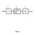
- FIG. 2 is a block diagram which illustrates a part of a first embodiment of the integrated digital circuit according to the invention in a general manner.
- the circuit of FIG. 2 comprises an input buffer 21 .
- the input of the input buffer 21 constitutes at the same time the input of the presented circuit.
- the output of the input buffer 21 is connected to the input of a non-volatile storage element 22 , which can be programmed in a non-destructive manner.
- the output of the non-volatile storage element 22 is connected to an input of an output buffer 23 .
- the output of the output buffer 23 constitutes at the same time the output of the presented circuit.
- the input buffer 21 and the output buffer 23 form a logic circuit portion which takes one of at least two different logic states in accordance with provided control signals.
- the input buffer 21 buffers a state represented by the input signal ‘B’ as long as power is supplied to the input buffer 21 and as long as no other input signal ‘B’ is applied.
- the buffered state is programmed automatically and immediately into the non-volatile storage element 22 , which provides a corresponding signal to the output buffer 23 .
- the output buffer 23 buffers the state corresponding to the signal from the non-volatile storage element 22 as long as power is supplied to the output buffer 21 and as long as no other signal is received.
- the output buffer 21 provides a signal corresponding to the buffered state as output signal ‘out’.
- the buffered states of the buffers 21 , 23 are lost. But the non-volatile storage element 22 stores the programmed state independently of power supply. When the power supply is switched on again, the output buffer 23 will therefore receive from the non-volatile storage element 22 immediately a signal corresponding to the previously buffered state again. As a result, the output buffer 23 is immediately able to provide the output signal ‘out’ again which was output before the power was switched off.
- FIG. 3 illustrates by way of example a modified CMOS latch as one of several possibilities of realizing the circuit of FIG. 2 .
- the modified CMOS latch proceeds from the CMOS latch of FIG. 1 .
- the CMOS latch of FIG. 3 comprises an p-channel enhancement MOSFET T 31 and a n-channel enhancement MOSFET T 32 .
- the source of the p-channel MOSFET T 31 is connected to a power supply Vdd.
- the drain of the p-channel MOSFET T 31 is connected to the drain of the n-channel MOSFET T 32 .
- the source of the n-channel MOSFET T 32 is connected to ground Gnd.
- the gate of the p-channel MOSFET T 3 , and the gate of the n-channel MOSFET T 32 are connected to a clocked input “in”.
- the clocking is represented by a switch clk arranged between the input “in” and the gates.
- the connection between the p-channel MOSFET T 3 , and the n-channel MOSFET T 32 is connected to an output “out” of the CMOS latch.
- MOSFETs T 31 and T 32 constitute in this embodiment the logic circuit portion of the integrated digital circuit according to the invention.
- a non-volatile storage element C is arranged between the connection between the p-channel MOSFET T 31 and the n-channel MOSFET T 32 on the one hand and ground Gnd on the other hand.
- the non-volatile storage element C is a capacitor with a ferro electric dielectricum or a magneto static element.
- the basic function of the circuit of FIG. 3 is the same as the basic function of the circuit of FIG. 1 . That is, when a low input voltage is provided to the input “in” of the CMOS latch, the p-channel MOSFET T 31 is conductive while the n-channel MOSFET T 32 is blocking. As a result, the output voltage at the output “out” is high. When a high input voltage is provided to the input “in” of the CMOS latch, the n-channel MOSFET T 32 is conductive while the p-channel MOSFET T 31 is blocking. As a result, the output voltage at the output “out” is low.
- the respective status of the transistor arrangement is stored immediately in the non-volatile storage element C, since this storage element C is connected to the output “out” of the CMOS latch.
- the output voltage is used more specifically for programming the non-volatile storage element C, the programming of a non-volatile storage element by applying a voltage per se being well known.
- the programming of a ferro-electric material is described for instance in the above cited web-site “http://www.ramtron.com/”.
- the non-volatile storage element C will store the current logic status for an unlimited time and independently of power supply Vdd, as long as no reprogramming occurs. Thus, the digital circuit can be stopped and even be powered down after each clock cycle without loosing information. When the digital circuit is powered up again, the status of the CMOS latch is immediately available at the output “out”, since the status is made available by the non-volatile storage element C.
- FIG. 4 illustrates another modified CMOS latch as part of a second embodiment of an integrated digital circuit according to the invention.
- the circuit of FIG. 4 comprises a pair of CMOS transistors T 41 , T 42 , which is arranged between a voltage supply Vdd and ground Gnd and which is connected to a clocked input “in” and to an output “out”.
- the clocking is represented again by a switch clk arranged between the input “in” and the gates of the transistors T 41 , T 42 .
- the basic functions of the pair of CMOS transistors T 41 , T 42 for providing a high and a low output voltage at output “out” is the same as in the embodiment presented in FIG. 2 .
- MOSFETs T 41 and T 42 thus constitute in this embodiment the logic circuit portion of the integrated digital circuit according to the invention.
- a non-volatile storage component is integrated directly into the transistors T 41 , T 42 .
- the transistors T 41 , T 42 themselves thus store directly the respective status of the CMOS latch in a non-volatile manner.
Abstract
Description
Claims (6)
Priority Applications (5)
| Application Number | Priority Date | Filing Date | Title |
|---|---|---|---|
| US10/372,721 US6876226B2 (en) | 2003-02-24 | 2003-02-24 | Integrated digital circuit |
| PCT/IB2004/000514 WO2004075404A1 (en) | 2003-02-24 | 2004-02-18 | Integrated digital circuit comprising a non-volatile storage element |
| CNA2004800050359A CN1778043A (en) | 2003-02-24 | 2004-02-18 | Integrated digital circuit comprising a non-volatile storage element |
| KR1020057013067A KR100720700B1 (en) | 2003-02-24 | 2004-02-18 | Integrated digital circuit comprising a non-volatile storage element |
| EP04712121A EP1599940A1 (en) | 2003-02-24 | 2004-02-18 | Integrated digital circuit comprising a non-volatile storage element |
Applications Claiming Priority (1)
| Application Number | Priority Date | Filing Date | Title |
|---|---|---|---|
| US10/372,721 US6876226B2 (en) | 2003-02-24 | 2003-02-24 | Integrated digital circuit |
Publications (2)
| Publication Number | Publication Date |
|---|---|
| US20040164764A1 US20040164764A1 (en) | 2004-08-26 |
| US6876226B2 true US6876226B2 (en) | 2005-04-05 |
Family
ID=32868575
Family Applications (1)
| Application Number | Title | Priority Date | Filing Date |
|---|---|---|---|
| US10/372,721 Expired - Lifetime US6876226B2 (en) | 2003-02-24 | 2003-02-24 | Integrated digital circuit |
Country Status (5)
| Country | Link |
|---|---|
| US (1) | US6876226B2 (en) |
| EP (1) | EP1599940A1 (en) |
| KR (1) | KR100720700B1 (en) |
| CN (1) | CN1778043A (en) |
| WO (1) | WO2004075404A1 (en) |
Cited By (3)
| Publication number | Priority date | Publication date | Assignee | Title |
|---|---|---|---|---|
| US20070075140A1 (en) * | 2005-10-04 | 2007-04-05 | Gregory Guez | Means to deactivate a contactless device |
| US8680776B1 (en) | 2011-12-20 | 2014-03-25 | Universal Lighting Technologies, Inc. | Lighting device including a fast start circuit for regulating power supply to a PFC controller |
| US9742403B2 (en) | 2013-04-02 | 2017-08-22 | Hewlett Packard Enterprise Development Lp | State-retaining logic cell |
Families Citing this family (2)
| Publication number | Priority date | Publication date | Assignee | Title |
|---|---|---|---|---|
| US8373438B2 (en) * | 2010-10-29 | 2013-02-12 | Alexander Mikhailovich Shukh | Nonvolatile logic circuit |
| US20140159770A1 (en) * | 2012-12-12 | 2014-06-12 | Alexander Mikhailovich Shukh | Nonvolatile Logic Circuit |
Citations (9)
| Publication number | Priority date | Publication date | Assignee | Title |
|---|---|---|---|---|
| EP0415221A2 (en) | 1989-08-28 | 1991-03-06 | National Semiconductor Corporation | Non-volatile programmable interconnection circuit |
| US5434811A (en) | 1987-11-19 | 1995-07-18 | National Semiconductor Corporation | Non-destructive read ferroelectric based memory circuit |
| JPH08180671A (en) | 1994-12-22 | 1996-07-12 | Matsushita Electric Ind Co Ltd | Semiconductor memory |
| GB2315348A (en) | 1996-07-13 | 1998-01-28 | Plessey Semiconductors Ltd | Programmable logic arrays |
| US5923184A (en) * | 1996-12-23 | 1999-07-13 | Motorola, Inc. | Ferroelectric transistor logic functions for programming |
| JP2000077986A (en) | 1998-09-02 | 2000-03-14 | Rohm Co Ltd | Sequential circuit using ferroelectric and semiconductor device using the circuit |
| US6233169B1 (en) | 1998-11-06 | 2001-05-15 | Rohm Co., Ltd. | Signal storing circuit semiconductor device, gate array and IC-card |
| JP2002269969A (en) | 2001-03-07 | 2002-09-20 | Nec Corp | Memory cell, non-volatile memory device, and its control method |
| US6710624B2 (en) * | 2000-01-21 | 2004-03-23 | Richard M. Lienau | Programmable array logic circuit macrocell using ferromagnetic memory cells |
Family Cites Families (1)
| Publication number | Priority date | Publication date | Assignee | Title |
|---|---|---|---|---|
| JP3642559B2 (en) * | 1998-11-06 | 2005-04-27 | ローム株式会社 | Signal holding circuit, semiconductor device, gate array, and IC card |
-
2003
- 2003-02-24 US US10/372,721 patent/US6876226B2/en not_active Expired - Lifetime
-
2004
- 2004-02-18 EP EP04712121A patent/EP1599940A1/en not_active Withdrawn
- 2004-02-18 WO PCT/IB2004/000514 patent/WO2004075404A1/en active Application Filing
- 2004-02-18 CN CNA2004800050359A patent/CN1778043A/en active Pending
- 2004-02-18 KR KR1020057013067A patent/KR100720700B1/en not_active IP Right Cessation
Patent Citations (10)
| Publication number | Priority date | Publication date | Assignee | Title |
|---|---|---|---|---|
| US5434811A (en) | 1987-11-19 | 1995-07-18 | National Semiconductor Corporation | Non-destructive read ferroelectric based memory circuit |
| EP0415221A2 (en) | 1989-08-28 | 1991-03-06 | National Semiconductor Corporation | Non-volatile programmable interconnection circuit |
| JPH08180671A (en) | 1994-12-22 | 1996-07-12 | Matsushita Electric Ind Co Ltd | Semiconductor memory |
| GB2315348A (en) | 1996-07-13 | 1998-01-28 | Plessey Semiconductors Ltd | Programmable logic arrays |
| US5923184A (en) * | 1996-12-23 | 1999-07-13 | Motorola, Inc. | Ferroelectric transistor logic functions for programming |
| JP2000077986A (en) | 1998-09-02 | 2000-03-14 | Rohm Co Ltd | Sequential circuit using ferroelectric and semiconductor device using the circuit |
| US6314016B1 (en) * | 1998-09-02 | 2001-11-06 | Rohm Co., Ltd. | Sequential circuits using ferroelectrics and semiconductor devices using the same |
| US6233169B1 (en) | 1998-11-06 | 2001-05-15 | Rohm Co., Ltd. | Signal storing circuit semiconductor device, gate array and IC-card |
| US6710624B2 (en) * | 2000-01-21 | 2004-03-23 | Richard M. Lienau | Programmable array logic circuit macrocell using ferromagnetic memory cells |
| JP2002269969A (en) | 2001-03-07 | 2002-09-20 | Nec Corp | Memory cell, non-volatile memory device, and its control method |
Cited By (4)
| Publication number | Priority date | Publication date | Assignee | Title |
|---|---|---|---|---|
| US20070075140A1 (en) * | 2005-10-04 | 2007-04-05 | Gregory Guez | Means to deactivate a contactless device |
| US7548164B2 (en) * | 2005-10-04 | 2009-06-16 | Atmel Corporation | Means to deactivate a contactless device |
| US8680776B1 (en) | 2011-12-20 | 2014-03-25 | Universal Lighting Technologies, Inc. | Lighting device including a fast start circuit for regulating power supply to a PFC controller |
| US9742403B2 (en) | 2013-04-02 | 2017-08-22 | Hewlett Packard Enterprise Development Lp | State-retaining logic cell |
Also Published As
| Publication number | Publication date |
|---|---|
| KR20050090004A (en) | 2005-09-09 |
| CN1778043A (en) | 2006-05-24 |
| US20040164764A1 (en) | 2004-08-26 |
| KR100720700B1 (en) | 2007-05-21 |
| EP1599940A1 (en) | 2005-11-30 |
| WO2004075404A1 (en) | 2004-09-02 |
Similar Documents
| Publication | Publication Date | Title |
|---|---|---|
| US8242826B2 (en) | Retention flip-flop | |
| US7164301B2 (en) | State retention power gating latch circuit | |
| RU2321944C2 (en) | Power-independent multi-threshold cmos trigger with leak control | |
| US6850103B2 (en) | Low leakage single-step latch circuit | |
| US7982514B2 (en) | State-retentive master-slave flip flop to reduce standby leakage current | |
| TWI625939B (en) | Electronic circuit | |
| US20180159513A1 (en) | Retention Flip-Flop Circuits For Low Power Applications | |
| US20010020858A1 (en) | Latch circuit and semiconductor integrated circuit having the latch circuit with control signal having a large voltage amplitude | |
| US20070085585A1 (en) | Data retention in operational and sleep modes | |
| TWI556235B (en) | Memory cell with retention using resistive memory | |
| JP2013131242A (en) | Non-volatile state retention latch | |
| JP2002064150A (en) | Semiconductor device | |
| JP2007535031A (en) | State retention in data processing systems | |
| JPH10261946A (en) | Semiconductor integrated circuit | |
| JP2005167184A (en) | Semiconductor integrated circuit device | |
| TW200415851A (en) | Method for reducing power consumption in a state retaining circuit, state retaining circuit and electronic device | |
| KR100355436B1 (en) | Semiconductor integrated circuit device having power reduction mechanism | |
| JP2000312136A (en) | Flip-flop circuit | |
| US6876226B2 (en) | Integrated digital circuit | |
| JP6252934B2 (en) | Logic circuit with power saving function | |
| US10373677B2 (en) | Semiconductor device to reduce energy consumed to write data | |
| US7917776B2 (en) | System-on-chip including deepstop mode to reduce total leakage current and method thereof | |
| US10340899B2 (en) | High performance low retention mode leakage flip-flop | |
| JP3567159B2 (en) | Semiconductor integrated circuit with power reduction mechanism | |
| JP3033719B2 (en) | Low power semiconductor integrated circuit |
Legal Events
| Date | Code | Title | Description |
|---|---|---|---|
| AS | Assignment |
Owner name: NOKIA CORPORATION, FINLAND Free format text: ASSIGNMENT OF ASSIGNORS INTEREST;ASSIGNORS:BUCHMANN, MICHAEL;UFFMANN, DIRK;REEL/FRAME:014170/0231 Effective date: 20030404 |
|
| STCF | Information on status: patent grant |
Free format text: PATENTED CASE |
|
| FPAY | Fee payment |
Year of fee payment: 4 |
|
| FPAY | Fee payment |
Year of fee payment: 8 |
|
| AS | Assignment |
Owner name: NOKIA TECHNOLOGIES OY, FINLAND Free format text: ASSIGNMENT OF ASSIGNORS INTEREST;ASSIGNOR:NOKIA CORPORATION;REEL/FRAME:035600/0122 Effective date: 20150116 |
|
| FPAY | Fee payment |
Year of fee payment: 12 |
|
| AS | Assignment |
Owner name: PROVENANCE ASSET GROUP LLC, CONNECTICUT Free format text: ASSIGNMENT OF ASSIGNORS INTEREST;ASSIGNORS:NOKIA TECHNOLOGIES OY;NOKIA SOLUTIONS AND NETWORKS BV;ALCATEL LUCENT SAS;REEL/FRAME:043877/0001 Effective date: 20170912 Owner name: NOKIA USA INC., CALIFORNIA Free format text: SECURITY INTEREST;ASSIGNORS:PROVENANCE ASSET GROUP HOLDINGS, LLC;PROVENANCE ASSET GROUP LLC;REEL/FRAME:043879/0001 Effective date: 20170913 Owner name: CORTLAND CAPITAL MARKET SERVICES, LLC, ILLINOIS Free format text: SECURITY INTEREST;ASSIGNORS:PROVENANCE ASSET GROUP HOLDINGS, LLC;PROVENANCE ASSET GROUP, LLC;REEL/FRAME:043967/0001 Effective date: 20170913 |
|
| AS | Assignment |
Owner name: NOKIA US HOLDINGS INC., NEW JERSEY Free format text: ASSIGNMENT AND ASSUMPTION AGREEMENT;ASSIGNOR:NOKIA USA INC.;REEL/FRAME:048370/0682 Effective date: 20181220 |
|
| AS | Assignment |
Owner name: PROVENANCE ASSET GROUP LLC, CONNECTICUT Free format text: RELEASE BY SECURED PARTY;ASSIGNOR:CORTLAND CAPITAL MARKETS SERVICES LLC;REEL/FRAME:058983/0104 Effective date: 20211101 Owner name: PROVENANCE ASSET GROUP HOLDINGS LLC, CONNECTICUT Free format text: RELEASE BY SECURED PARTY;ASSIGNOR:CORTLAND CAPITAL MARKETS SERVICES LLC;REEL/FRAME:058983/0104 Effective date: 20211101 Owner name: PROVENANCE ASSET GROUP LLC, CONNECTICUT Free format text: RELEASE BY SECURED PARTY;ASSIGNOR:NOKIA US HOLDINGS INC.;REEL/FRAME:058363/0723 Effective date: 20211129 Owner name: PROVENANCE ASSET GROUP HOLDINGS LLC, CONNECTICUT Free format text: RELEASE BY SECURED PARTY;ASSIGNOR:NOKIA US HOLDINGS INC.;REEL/FRAME:058363/0723 Effective date: 20211129 |
|
| AS | Assignment |
Owner name: RPX CORPORATION, CALIFORNIA Free format text: ASSIGNMENT OF ASSIGNORS INTEREST;ASSIGNOR:PROVENANCE ASSET GROUP LLC;REEL/FRAME:059352/0001 Effective date: 20211129 |