US6909152B2 - High density DRAM with reduced peripheral device area and method of manufacture - Google Patents
High density DRAM with reduced peripheral device area and method of manufacture Download PDFInfo
- Publication number
- US6909152B2 US6909152B2 US10/294,329 US29432902A US6909152B2 US 6909152 B2 US6909152 B2 US 6909152B2 US 29432902 A US29432902 A US 29432902A US 6909152 B2 US6909152 B2 US 6909152B2
- Authority
- US
- United States
- Prior art keywords
- gate
- dielectric layer
- contact
- dielectric
- semiconductor device
- Prior art date
- Legal status (The legal status is an assumption and is not a legal conclusion. Google has not performed a legal analysis and makes no representation as to the accuracy of the status listed.)
- Expired - Lifetime, expires
Links
Images


Classifications
-
- H—ELECTRICITY
- H10—SEMICONDUCTOR DEVICES; ELECTRIC SOLID-STATE DEVICES NOT OTHERWISE PROVIDED FOR
- H10B—ELECTRONIC MEMORY DEVICES
- H10B12/00—Dynamic random access memory [DRAM] devices
- H10B12/01—Manufacture or treatment
- H10B12/09—Manufacture or treatment with simultaneous manufacture of the peripheral circuit region and memory cells
-
- H—ELECTRICITY
- H10—SEMICONDUCTOR DEVICES; ELECTRIC SOLID-STATE DEVICES NOT OTHERWISE PROVIDED FOR
- H10B—ELECTRONIC MEMORY DEVICES
- H10B12/00—Dynamic random access memory [DRAM] devices
- H10B12/01—Manufacture or treatment
- H10B12/02—Manufacture or treatment for one transistor one-capacitor [1T-1C] memory cells
- H10B12/05—Making the transistor
Definitions
- This invention relates to dynamic random access memory (DRAM) structures, and more particularly, to high density DRAMs with reduced peripheral device area and a method of manufacturing the same.
- DRAM dynamic random access memory
- a state-of-the art DRAM comprises a substrate with an array of memory cells, including transistors, that are arranged in rows and columns and connected by wordlines and bitlines and a peripheral device area with support circuitry, including transistors, for reading in and out binary digits (bits) stored in the memory cells.
- array transistors are all the same and are packed very densely in the array while peripheral transistors differ in size and are spaced further apart.
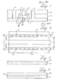
- FIGS. 1 and 2 illustrate a prior art peripheral metal oxide semiconductor (MOS) transistor 1 in 0.14 ⁇ m groundrule.
- the MOS transistor is formed on a silicon substrate 3 and comprises a thin gate oxide layer 5 on the substrate.
- the gate oxide layer is silicon oxide and has a thickness of about 50 A.
- the MOS transistor further comprises a gate conductor 7 , a gate cap insulator 9 , two spacers 11 , a dielectric layer 13 , and a layer of silicon dioxide 15 . Spaced apart and on either side of the gate conductor are periphery contact-to-diffusion (CD) openings or CD contacts 17 , which form a source and a drain for the MOS transistor 1 .
- CD periphery contact-to-diffusion
- the terms “drain” and “source” are used herein interchangeably to refer to the diffusion regions.
- the CD contacts are interconnected separately for the source and the drain by conductive metalization lines 19 .
- a contact-to-gate (CG) opening or CG contact 21 forms a contact to the gate conductor 7 .
- the separation 23 between the CD contacts 17 and the gate conductor 7 is 0.14 ⁇ m, and the separation 25 between the metalization lines is 0.38 ⁇ m.
- the distance between the metalization lines which includes the width of the gate conductor and the width of the CD contacts, determines the overall width of the transistor.
- the overall width 27 of the prior art MOS transistor in FIG. 2 is 0.94 ⁇ m.
- the CD contacts 17 and the CG contacts 21 are patterned on the same photoresist mask, and then etched at the same time.
- a non-selective etching process is used to etch the CD and CG contacts because the contacts need to be etched through a thick layer of gate cap insulator 9 which is usually silicon nitride.
- the spacing between the gate conductor 7 and the CD contacts 17 must be at least 0.14 ⁇ m because a non-selective etch process is used. If the CD contacts 17 are closer than 0.14 ⁇ m to the gate conductor 7 , the non-selective etching process may etch into the gate conductor if there is mask overlay shift and cause a short in the path.
- a method for forming a semiconductor structure. The method includes: providing a substrate, forming a gate oxide layer on the substrate, depositing a gate conductor layer over the gate oxide; depositing a gate cap insulator over the gate conductor; etching a gate stack having sidewalls from the gate conductor and the gate cap insulator, forming spacers on the gate stack sidewalls; implanting at least one source and one drain; depositing a first insulating layer over the substrate; depositing a second dielectric layer over the substrate, forming at least one borderless array contact (CB) and at least one peripheral contact-to-diffusion simultaneously using a selective etching process; and etching at least one gate contact.
- CB borderless array contact
- metallization trenches are formed after etching the gate contact. Subsequently, the metallization trenches, borderless array contact, peripheral contact-to-diffusion, and the gate contact are filled with a conductive material to form a semiconductor device.
- a semiconductor structure comprising a substrate having an array region and a support region. Gate stacks having a gate conductor, a gate cap, and sidewall spacers are positioned on the substrate. A first layer of dielectric material covers the gate stacks and substrate, and a second layer of dielectric material covers the first dielectric layer. Peripheral contacts-to-diffusion extend from the second dielectric layer to the substrate, and borderless array contacts extend from the insulating layer to the gate conductor. The peripheral contacts-to-diffusion and borderless array contacts are formed using the same photoresist mask and etched using a process which is nonselective to the gate cap and spacers.
- One advantage of the present invention is that the peripheral transistor area that is necessary for mask layout is decreased.
- Another advantage of the present invention is that the overall width of the peripheral transistor is significantly reduced, so that the transistor occupies less area on the silicon wafer. As a result, more DRAMs can be printed on a given wafer area.
- a further advantage of the present invention is that the overall width of the peripheral transistors is reduced without adding any additional manufacturing steps.
- FIG. 1 is cross-section of a prior art MOS transistor used in the peripheral circuitry for a DRAM device
- FIG. 2 is a top view of a prior art MOS transistor used in the peripheral circuitry for a DRAM device
- FIGS. 3-12 are cross-sections of a portion of a substrate, at various stages of manufacture, on which MOS transistors suitable for DRAM memory array cells and peripheral circuitry are formed;
- FIG. 13 is top view of a peripheral MOS transistor of the present invention.
- FIG. 3 shows a portion of a substrate 31 , which comprises an array portion where N-MOSFETs are formed for the memory cells of a DRAM, and a periphery portion where N-MOSFETs and P-MOSFETS are formed for the support circuitry of the DRAM.
- the support circuitry is concentrated in regions that border the area where the memory cells are concentrated.
- the substrate 31 may be monocrystalline silicon or any other suitable semiconductor substrate material.
- a masking layer of suitable photoresist (not shown) is deposited on the substrate and patterned.
- the substrate is subjected to ion implantation to form transistor wells.
- the masking layer is stripped and a gate oxide layer 37 is grown over the entire surface of the crystalline substrate 31 as shown in FIG. 3 .
- a gate conductor 39 is then deposited on the gate oxide layer 37 as shown in FIG. 4 .
- the gate conductor 39 may be undoped polysilicon, doped polysilicon and/or polycide, although other suitable conductors, including metal may also be used.
- the gate conductor 39 is formed by depositing a bottom layer of polysilicon on the gate oxide 37 layer and then depositing a layer of tungsten silicide (WSi) over the polysilicon layer by either sputtering or chemical vapor deposition (CVD).
- the bottom layer of polysilicon improves the adhesion of the tungsten silicide to the gate oxide layer.
- the polysilicon layer may be doped in order to improve its conductivity. However, depending on the desired threshold voltage for the device, the doping concentration may or may not be uniform with respect to the depth of the polysilicon layer.
- a gate cap insulator layer 41 is then deposited over the gate conductor layer 39 as shown in FIG. 5 .
- the gate cap insulator layer may be silicon nitride, silicon dioxide, doped silicon dioxide, or any other suitable material.
- a layer of suitable photoresist (not shown) is deposited over the gate cap insulator 41 and patterned to form the gate stack mask.
- gate stacks 43 comprising gate conductor 39 and gate cap insulator 41 are etched.
- the gate stacks 41 are etched using a standard reactive ion etching (RIE) process utilizing standard chemistries, including but not limited to, carbon monoxide, nitrogen, oxygen, Argon, C 4 F 8 , CH 2 F 2 , and CHF 3 .
- RIE reactive ion etching
- other suitable directional etching processes well-known in the art of semiconductor processing may also be used.
- the mask is stripped and gate spacers 47 are created on sidewalls 45 of the gate stacks.
- a uniform layer of insulating material is deposited by CVD, or by any other suitable method, on the gate stacks 43 and the gate oxide layer 37 .
- the vertical thickness of the insulating material on the gate oxide layer 37 is the same as the horizontal thickness of the insulating layer on the sides of the gate stacks 43 .
- the vertical thickness of the insulating layer on the sides of the gate stacks 43 is generally the same as the height of the gate stacks 43 .
- the top of the gate stack and substrate will be etched away first leaving some insulating material on the sidewalls 45 of the gate stacks which are the gate spacers 47 .
- the spacers are formed from silicon nitride and etched using an anisotropic process such as a standard RIE etching process.
- an anisotropic process such as a standard RIE etching process.
- other insulating materials and etching processes well-known in the art may also be used.
- a source/drain implant mask 49 is deposited and patterned, and the source 51 and drain 53 are formed by ion implantation as shown by the arrows in FIG. 8 .
- the remaining source/drain mask is stripped, and a first dielectric layer 55 is deposited on the substrate.
- the first dielectric layer includes, but is not limited to borophosphosilicate insulating glass (BPSG), phosphosilicate insulating glass (PSG), FSG, F-BSG, and ASG.
- the first insulating layer is BPSG which may be deposited by a variety of methods including but not limited to, CVD, low pressure CVD, or plasma enhanced chemical vapor deposition (PECVD).
- Thermal reflow is used to fill the gaps so that a smooth contoured surface is formed over the substrate.
- the BPSG may have a relatively high amount of boron or phosphorous to accommodate the reflow-temperature of small geometry devices.
- the BPSG layer still roughly conforms to the underlying device features on the substrate, and therefore, is non-planar.
- the surface 57 of the BPSG glass is planarized by chemical mechanical polishing (CMP).
- a second dielectric layer 59 is deposited on the first dielectric layer.
- This dielectric layer may be tetraethylorthosilicate (TEOS), silicon dioxide, or any other suitable insulating material as shown in FIG. 9.
- TEOS tetraethylorthosilicate
- a DRAM array contact mask (not shown) is deposited on the TEOS layer and patterned by standard lithography.
- the DRAM array contacts 61 which are borderless contacts, and the periphery CD contacts 63 are then etched using an etching process selective to the material of the gate cap insulator 41 and spacers 47 as shown in FIG. 10 .
- the DRAM array contacts 61 and the peripheral CD 63 contacts can be etched at the same time because they are etched through similar materials.
- the gate cap insulator 41 and spacers 47 are silicon nitride and the etch is an RIE process selective to silicon nitride.
- the RIE process will not etch through silicon nitride gate spacers 47 and gate conductor 7 and cause a short in the gate path if the mask is misaligned.
- the CD contacts are not etched into the gate cap insulator or gate spacers. As a result, the CD contacts may be placed closer to the gate conductor without risking etch-out of the gate conductor thereby reducing the overall width of the MOS transistor.
- the DRAM array contact mask is stripped, and a DRAM peripheral contact mask (not shown) is deposited on the structure.
- the mask is patterned using standard lithography, and the silicon oxide layer and the gate cap insulator layer are etched using a non-selective etching process to form the CG contacts as shown in FIG. 11 .
- a standard non-selective RIE etch is used to etch the CG contacts.
- the DRAM peripheral contact mask is then stripped, and a line mask (not shown) for the first metalization layer is deposited on the structure.
- the mask is patterned using standard lithography, and first metalization trenches are etched into the silicon oxide layer. In one embodiment, a RIE process is used to etch the first metalization trenches.
- the remaining mask is then stripped, and a conductor 67 is deposited on the structure, filling in the array CB contacts 61 , the CD contacts 63 , and the CG contacts 65 , and first metalization trenches 69 as shown in FIG. 12 .
- the first metalization trenches are then planarized to the silicon oxide surface by a CMP process.
- the conductor may be tungsten, aluminum, aluminum-copper alloy, copper, tantalum, or any other suitable conductive material.
- FIG. 13 shows a top view of a peripheral MOS transistor of the current invention in which the CD contacts 63 have been moved closer to the gate conductor 39 .
- the distance 75 between the CD contacts 63 and the gate conductor 39 has been reduced from 0.14 ⁇ m to 0.075 m, and the distance 73 between the metallization lines 71 has been reduced from 0.38 ⁇ m to 0.25 m.
- the overall width of the transistor 77 has been reduced by 0.13 ⁇ m from 0.94 ⁇ m to 0.81 m which represents about a 14% percent decrease in size of the transistor. While the present invention has been discussed in terms of DRAM devices having transistors in 0.14 ⁇ m ground rule, it will be apparent to those skilled in the art that the present invention will be applicable to DRAM devices and other semiconductor devices utilizing transistors having smaller groundrules.
Abstract
Description
Claims (9)
Priority Applications (3)
| Application Number | Priority Date | Filing Date | Title |
|---|---|---|---|
| US10/294,329 US6909152B2 (en) | 2002-11-14 | 2002-11-14 | High density DRAM with reduced peripheral device area and method of manufacture |
| DE10347428A DE10347428B4 (en) | 2002-11-14 | 2003-10-13 | A high density DRAM manufacturing method with reduced peripheral device area |
| US11/003,592 US7163891B2 (en) | 2002-11-14 | 2004-12-03 | High density DRAM with reduced peripheral device area and method of manufacture |
Applications Claiming Priority (1)
| Application Number | Priority Date | Filing Date | Title |
|---|---|---|---|
| US10/294,329 US6909152B2 (en) | 2002-11-14 | 2002-11-14 | High density DRAM with reduced peripheral device area and method of manufacture |
Related Child Applications (1)
| Application Number | Title | Priority Date | Filing Date |
|---|---|---|---|
| US11/003,592 Division US7163891B2 (en) | 2002-11-14 | 2004-12-03 | High density DRAM with reduced peripheral device area and method of manufacture |
Publications (2)
| Publication Number | Publication Date |
|---|---|
| US20040094810A1 US20040094810A1 (en) | 2004-05-20 |
| US6909152B2 true US6909152B2 (en) | 2005-06-21 |
Family
ID=32229793
Family Applications (2)
| Application Number | Title | Priority Date | Filing Date |
|---|---|---|---|
| US10/294,329 Expired - Lifetime US6909152B2 (en) | 2002-11-14 | 2002-11-14 | High density DRAM with reduced peripheral device area and method of manufacture |
| US11/003,592 Expired - Fee Related US7163891B2 (en) | 2002-11-14 | 2004-12-03 | High density DRAM with reduced peripheral device area and method of manufacture |
Family Applications After (1)
| Application Number | Title | Priority Date | Filing Date |
|---|---|---|---|
| US11/003,592 Expired - Fee Related US7163891B2 (en) | 2002-11-14 | 2004-12-03 | High density DRAM with reduced peripheral device area and method of manufacture |
Country Status (2)
| Country | Link |
|---|---|
| US (2) | US6909152B2 (en) |
| DE (1) | DE10347428B4 (en) |
Cited By (2)
| Publication number | Priority date | Publication date | Assignee | Title |
|---|---|---|---|---|
| US20100210760A1 (en) * | 2007-03-28 | 2010-08-19 | Yuichi Kitagawa | Process for manufacturing modified conjugated diene polymer, composition comprising the polymer, and tire comprising the composition |
| US20120273879A1 (en) * | 2011-04-27 | 2012-11-01 | Shekar Mallikarjunaswamy | Top drain ldmos |
Families Citing this family (12)
| Publication number | Priority date | Publication date | Assignee | Title |
|---|---|---|---|---|
| KR100505062B1 (en) * | 2003-02-22 | 2005-07-29 | 삼성전자주식회사 | Method of manufacturing semiconductor device |
| US7256112B2 (en) * | 2005-01-20 | 2007-08-14 | Chartered Semiconductor Manufacturing, Ltd | Laser activation of implanted contact plug for memory bitline fabrication |
| US7521353B2 (en) * | 2005-03-25 | 2009-04-21 | Sandisk 3D Llc | Method for reducing dielectric overetch when making contact to conductive features |
| US7422985B2 (en) * | 2005-03-25 | 2008-09-09 | Sandisk 3D Llc | Method for reducing dielectric overetch using a dielectric etch stop at a planar surface |
| KR100632046B1 (en) * | 2005-07-05 | 2006-10-04 | 동부일렉트로닉스 주식회사 | Gate line of semiconductor device and method for manufacturing thereof |
| US8436404B2 (en) * | 2009-12-30 | 2013-05-07 | Intel Corporation | Self-aligned contacts |
| US8232607B2 (en) * | 2010-11-23 | 2012-07-31 | International Business Machines Corporation | Borderless contact for replacement gate employing selective deposition |
| US20130214289A1 (en) * | 2012-02-16 | 2013-08-22 | Texas Instruments Incorporated | Short-Resistant Metal-Gate MOS Transistor and Method of Forming the Transistor |
| CN108269762B (en) * | 2016-12-30 | 2021-06-08 | 联华电子股份有限公司 | Method for manufacturing semiconductor memory device |
| US10580783B2 (en) | 2018-03-01 | 2020-03-03 | Sandisk Technologies Llc | Multi-tier three-dimensional memory device containing differential etch rate field oxides and method of making the same |
| US11211324B2 (en) | 2019-09-18 | 2021-12-28 | Intel Corporation | Via contact patterning method to increase edge placement error margin |
| WO2021237407A1 (en) | 2020-05-25 | 2021-12-02 | Yangtze Memory Technologies Co., Ltd. | Memory device and method for forming the same |
Citations (9)
| Publication number | Priority date | Publication date | Assignee | Title |
|---|---|---|---|---|
| US5956594A (en) * | 1998-11-02 | 1999-09-21 | Vanguard International Semiconductor Corporation | Method for simultaneously forming capacitor plate and metal contact structures for a high density DRAM device |
| US6074912A (en) | 1999-02-08 | 2000-06-13 | United Microelectronics Corp. | Method for forming different area vias of dynamic random access memory |
| US6207513B1 (en) | 1999-11-02 | 2001-03-27 | Infineon Technologies North America Corp. | Spacer process to eliminate corner transistor device |
| US6235574B1 (en) | 1999-03-22 | 2001-05-22 | Infineon North America Corp. | High performance DRAM and method of manufacture |
| US6245629B1 (en) | 1999-03-25 | 2001-06-12 | Infineon Technologies North America Corp. | Semiconductor structures and manufacturing methods |
| US6255684B1 (en) | 1997-05-02 | 2001-07-03 | Infineon Technologies Ag | DRAM cell configuration and method for its production |
| US6274425B1 (en) * | 1998-12-30 | 2001-08-14 | Hyundai Electronics Industries Co., Ltd. | Method for manufacturing semiconductor device |
| US6281084B1 (en) | 1999-08-31 | 2001-08-28 | Infineon Technologies Corporation | Disposable spacers for improved array gapfill in high density DRAMs |
| US6310396B1 (en) | 1997-06-24 | 2001-10-30 | Infineon Technologies Ag | Semiconductor circuit apparatus and method for fabricating the semiconductor circuit apparatus |
Family Cites Families (14)
| Publication number | Priority date | Publication date | Assignee | Title |
|---|---|---|---|---|
| US5126907A (en) | 1989-05-24 | 1992-06-30 | Hitachi, Ltd. | Thin film magnetic head having at least one magnetic core member made at least partly of a material having a high saturation magnetic flux density |
| JPH10242419A (en) | 1997-02-27 | 1998-09-11 | Mitsubishi Electric Corp | Manufacture of semiconductor and semiconductor device |
| JPH11135779A (en) * | 1997-10-28 | 1999-05-21 | Toshiba Corp | Semiconductor device and manufacture thereof |
| KR100275725B1 (en) * | 1997-12-27 | 2000-12-15 | 윤종용 | Semiconductor memory device with triple well structure and manufacturing method therefor |
| TW410455B (en) * | 1998-02-16 | 2000-11-01 | United Microelectronics Corp | Forming method for dual damascene structure |
| US5893734A (en) * | 1998-09-14 | 1999-04-13 | Vanguard International Semiconductor Corporation | Method for fabricating capacitor-under-bit line (CUB) dynamic random access memory (DRAM) using tungsten landing plug contacts |
| US6323519B1 (en) * | 1998-10-23 | 2001-11-27 | Advanced Micro Devices, Inc. | Ultrathin, nitrogen-containing MOSFET sidewall spacers using low-temperature semiconductor fabrication process |
| US6133164A (en) * | 1999-02-23 | 2000-10-17 | Vantis Corporation | Fabrication of oxide regions having multiple thicknesses using minimized number of thermal cycles |
| US6248252B1 (en) * | 1999-02-24 | 2001-06-19 | Advanced Micro Devices, Inc. | Method of fabricating sub-micron metal lines |
| US6229198B1 (en) * | 1999-07-20 | 2001-05-08 | Advanced Micro Devices, Inc. | Non-uniform gate doping for reduced overlap capacitance |
| US6281059B1 (en) * | 2000-05-11 | 2001-08-28 | Worldwide Semiconductor Manufacturing Corp. | Method of doing ESD protective device ion implant without additional photo mask |
| US6555450B2 (en) | 2000-10-04 | 2003-04-29 | Samsung Electronics Co., Ltd. | Contact forming method for semiconductor device |
| US6664182B2 (en) * | 2001-04-25 | 2003-12-16 | Macronix International Co. Ltd. | Method of improving the interlayer adhesion property of low-k layers in a dual damascene process |
| TW483111B (en) * | 2001-06-08 | 2002-04-11 | Promos Technologies Inc | Method for forming contact of memory device |
-
2002
- 2002-11-14 US US10/294,329 patent/US6909152B2/en not_active Expired - Lifetime
-
2003
- 2003-10-13 DE DE10347428A patent/DE10347428B4/en not_active Expired - Fee Related
-
2004
- 2004-12-03 US US11/003,592 patent/US7163891B2/en not_active Expired - Fee Related
Patent Citations (9)
| Publication number | Priority date | Publication date | Assignee | Title |
|---|---|---|---|---|
| US6255684B1 (en) | 1997-05-02 | 2001-07-03 | Infineon Technologies Ag | DRAM cell configuration and method for its production |
| US6310396B1 (en) | 1997-06-24 | 2001-10-30 | Infineon Technologies Ag | Semiconductor circuit apparatus and method for fabricating the semiconductor circuit apparatus |
| US5956594A (en) * | 1998-11-02 | 1999-09-21 | Vanguard International Semiconductor Corporation | Method for simultaneously forming capacitor plate and metal contact structures for a high density DRAM device |
| US6274425B1 (en) * | 1998-12-30 | 2001-08-14 | Hyundai Electronics Industries Co., Ltd. | Method for manufacturing semiconductor device |
| US6074912A (en) | 1999-02-08 | 2000-06-13 | United Microelectronics Corp. | Method for forming different area vias of dynamic random access memory |
| US6235574B1 (en) | 1999-03-22 | 2001-05-22 | Infineon North America Corp. | High performance DRAM and method of manufacture |
| US6245629B1 (en) | 1999-03-25 | 2001-06-12 | Infineon Technologies North America Corp. | Semiconductor structures and manufacturing methods |
| US6281084B1 (en) | 1999-08-31 | 2001-08-28 | Infineon Technologies Corporation | Disposable spacers for improved array gapfill in high density DRAMs |
| US6207513B1 (en) | 1999-11-02 | 2001-03-27 | Infineon Technologies North America Corp. | Spacer process to eliminate corner transistor device |
Non-Patent Citations (1)
| Title |
|---|
| Peter Van Zant; Microchip Fabrication : a practical guide to semiconductor processing; 2000; McGraw Hill, New York; 4th edition; pp. 154-156, 391-392. * |
Cited By (3)
| Publication number | Priority date | Publication date | Assignee | Title |
|---|---|---|---|---|
| US20100210760A1 (en) * | 2007-03-28 | 2010-08-19 | Yuichi Kitagawa | Process for manufacturing modified conjugated diene polymer, composition comprising the polymer, and tire comprising the composition |
| US20120273879A1 (en) * | 2011-04-27 | 2012-11-01 | Shekar Mallikarjunaswamy | Top drain ldmos |
| US9159828B2 (en) * | 2011-04-27 | 2015-10-13 | Alpha And Omega Semiconductor Incorporated | Top drain LDMOS |
Also Published As
| Publication number | Publication date |
|---|---|
| US20040094810A1 (en) | 2004-05-20 |
| DE10347428B4 (en) | 2010-06-24 |
| US7163891B2 (en) | 2007-01-16 |
| US20050130352A1 (en) | 2005-06-16 |
| DE10347428A1 (en) | 2004-05-27 |
Similar Documents
| Publication | Publication Date | Title |
|---|---|---|
| JP4907838B2 (en) | Memory device having a recessed gate structure | |
| US8022455B2 (en) | Method of fabricating semiconductor device for reducing parasitic capacitance between bit lines and semiconductor device fabricated thereby | |
| KR100322218B1 (en) | Semiconductor device and method of manufacturing the same | |
| US6177340B1 (en) | Method to reduce contact hole aspect ratio for embedded DRAM arrays and logic devices, via the use of a tungsten bit line structure | |
| US6909152B2 (en) | High density DRAM with reduced peripheral device area and method of manufacture | |
| US6344389B1 (en) | Self-aligned damascene interconnect | |
| US6709945B2 (en) | Reduced aspect ratio digit line contact process flow used during the formation of a semiconductor device | |
| US6559499B1 (en) | Process for fabricating an integrated circuit device having capacitors with a multilevel metallization | |
| US11133248B2 (en) | Semiconductor structure and method for fabricating the same | |
| US5795804A (en) | Method of fabricating a stack/trench capacitor for a dynamic random access memory (DRAM) | |
| US8674404B2 (en) | Additional metal routing in semiconductor devices | |
| US6812092B2 (en) | Method for fabricating transistors having damascene formed gate contacts and self-aligned borderless bit line contacts | |
| US6960523B2 (en) | Method of reducing erosion of a nitride gate cap layer during reactive ion etch of nitride liner layer for bit line contact of DRAM device | |
| US6674111B2 (en) | Semiconductor device having a logic transistor therein | |
| US6271099B1 (en) | Method for forming a capacitor of a DRAM cell | |
| US6724054B1 (en) | Self-aligned contact formation using double SiN spacers | |
| US6680254B2 (en) | Method of fabricating bit line and bit line contact plug of a memory cell | |
| CN113241346A (en) | Semiconductor device and method of forming the same | |
| US6900118B2 (en) | Method for preventing contact defects in interlayer dielectric layer | |
| US7439125B2 (en) | Contact structure for a stack DRAM storage capacitor | |
| US6890815B2 (en) | Reduced cap layer erosion for borderless contacts | |
| US7195975B2 (en) | Method of forming bit line contact via | |
| US8093639B2 (en) | Method for fabricating a semiconductor device | |
| KR100487915B1 (en) | Capacitor Formation Method of Semiconductor Device | |
| US20050014332A1 (en) | Method to improve bitline contact formation using a line mask |
Legal Events
| Date | Code | Title | Description |
|---|---|---|---|
| AS | Assignment |
Owner name: INFINEON TECHNOLOGIES NORTH AMERICA CORP., CALIFOR Free format text: ASSIGNMENT OF ASSIGNORS INTEREST;ASSIGNORS:MALDEI, MICHAEL;COUSINEAU, BRIAN;GERSTMEIR, GUENTER;AND OTHERS;REEL/FRAME:013499/0692 Effective date: 20021106 |
|
| AS | Assignment |
Owner name: INFINEON TECHNOLOGIES, AG, GERMANY Free format text: ASSIGNMENT OF ASSIGNORS INTEREST;ASSIGNOR:INFINEON TECHNOLOGIES NORTH AMERICA CORP.;REEL/FRAME:013757/0941 Effective date: 20030620 |
|
| STCF | Information on status: patent grant |
Free format text: PATENTED CASE |
|
| FPAY | Fee payment |
Year of fee payment: 4 |
|
| AS | Assignment |
Owner name: QIMONDA AG, GERMANY Free format text: ASSIGNMENT OF ASSIGNORS INTEREST;ASSIGNOR:INFINEON TECHNOLOGIES AG;REEL/FRAME:023773/0001 Effective date: 20060425 Owner name: QIMONDA AG,GERMANY Free format text: ASSIGNMENT OF ASSIGNORS INTEREST;ASSIGNOR:INFINEON TECHNOLOGIES AG;REEL/FRAME:023773/0001 Effective date: 20060425 |
|
| FPAY | Fee payment |
Year of fee payment: 8 |
|
| AS | Assignment |
Owner name: INFINEON TECHNOLOGIES AG, GERMANY Free format text: ASSIGNMENT OF ASSIGNORS INTEREST;ASSIGNOR:QIMONDA AG;REEL/FRAME:035623/0001 Effective date: 20141009 |
|
| AS | Assignment |
Owner name: POLARIS INNOVATIONS LIMITED, IRELAND Free format text: ASSIGNMENT OF ASSIGNORS INTEREST;ASSIGNOR:INFINEON TECHNOLOGIES AG;REEL/FRAME:036818/0583 Effective date: 20150708 |
|
| FPAY | Fee payment |
Year of fee payment: 12 |
|
| SULP | Surcharge for late payment |
Year of fee payment: 11 |
|
| AS | Assignment |
Owner name: CHANGXIN MEMORY TECHNOLOGIES, INC, CHINA Free format text: ASSIGNMENT OF ASSIGNORS INTEREST;ASSIGNOR:POLARIS INNOVATIONS LIMITED;REEL/FRAME:051917/0581 Effective date: 20191130 |