US6951995B2 - Method and system for high-speed, precise micromachining an array of devices - Google Patents
Method and system for high-speed, precise micromachining an array of devices Download PDFInfo
- Publication number
- US6951995B2 US6951995B2 US10/397,541 US39754103A US6951995B2 US 6951995 B2 US6951995 B2 US 6951995B2 US 39754103 A US39754103 A US 39754103A US 6951995 B2 US6951995 B2 US 6951995B2
- Authority
- US
- United States
- Prior art keywords
- laser
- microns
- wavelength
- cuts
- subsystem
- Prior art date
- Legal status (The legal status is an assumption and is not a legal conclusion. Google has not performed a legal analysis and makes no representation as to the accuracy of the status listed.)
- Expired - Fee Related, expires
Links
- 238000005459 micromachining Methods 0.000 title claims abstract description 34
- 238000000034 method Methods 0.000 title abstract description 52
- 238000009966 trimming Methods 0.000 claims abstract description 57
- 238000005259 measurement Methods 0.000 claims abstract description 37
- 239000000463 material Substances 0.000 claims description 23
- 239000000758 substrate Substances 0.000 claims description 23
- 230000003287 optical effect Effects 0.000 claims description 17
- 239000010409 thin film Substances 0.000 claims description 14
- 238000001514 detection method Methods 0.000 claims description 6
- 238000005286 illumination Methods 0.000 claims description 4
- 239000007787 solid Substances 0.000 claims description 4
- 238000003708 edge detection Methods 0.000 claims description 2
- 239000004065 semiconductor Substances 0.000 claims description 2
- 239000000919 ceramic Substances 0.000 claims 1
- 230000035945 sensitivity Effects 0.000 claims 1
- 230000008569 process Effects 0.000 abstract description 13
- 238000005520 cutting process Methods 0.000 abstract description 12
- 230000000694 effects Effects 0.000 abstract description 3
- 238000012360 testing method Methods 0.000 abstract description 3
- WYTGDNHDOZPMIW-RCBQFDQVSA-N alstonine Natural products C1=CC2=C3C=CC=CC3=NC2=C2N1C[C@H]1[C@H](C)OC=C(C(=O)OC)[C@H]1C2 WYTGDNHDOZPMIW-RCBQFDQVSA-N 0.000 description 13
- 238000012545 processing Methods 0.000 description 12
- 239000004020 conductor Substances 0.000 description 8
- 239000000523 sample Substances 0.000 description 8
- 230000008859 change Effects 0.000 description 6
- 239000010408 film Substances 0.000 description 6
- 230000007246 mechanism Effects 0.000 description 6
- 230000001965 increasing effect Effects 0.000 description 5
- 230000001678 irradiating effect Effects 0.000 description 5
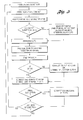
- 238000010586 diagram Methods 0.000 description 4
- 230000006872 improvement Effects 0.000 description 4
- 230000008901 benefit Effects 0.000 description 3
- 238000012937 correction Methods 0.000 description 3
- 238000013461 design Methods 0.000 description 3
- 238000007493 shaping process Methods 0.000 description 3
- 238000013459 approach Methods 0.000 description 2
- 238000003491 array Methods 0.000 description 2
- 230000003247 decreasing effect Effects 0.000 description 2
- 239000011159 matrix material Substances 0.000 description 2
- 238000012986 modification Methods 0.000 description 2
- 230000004048 modification Effects 0.000 description 2
- 230000010287 polarization Effects 0.000 description 2
- 230000008439 repair process Effects 0.000 description 2
- 238000000926 separation method Methods 0.000 description 2
- 238000004458 analytical method Methods 0.000 description 1
- 230000003466 anti-cipated effect Effects 0.000 description 1
- 230000015556 catabolic process Effects 0.000 description 1
- 238000010276 construction Methods 0.000 description 1
- 238000006880 cross-coupling reaction Methods 0.000 description 1
- 238000006731 degradation reaction Methods 0.000 description 1
- 238000009826 distribution Methods 0.000 description 1
- 238000005553 drilling Methods 0.000 description 1
- 238000005516 engineering process Methods 0.000 description 1
- 230000002708 enhancing effect Effects 0.000 description 1
- 229910052736 halogen Inorganic materials 0.000 description 1
- 150000002367 halogens Chemical class 0.000 description 1
- 238000010438 heat treatment Methods 0.000 description 1
- 238000003913 materials processing Methods 0.000 description 1
- 230000008018 melting Effects 0.000 description 1
- 238000002844 melting Methods 0.000 description 1
- 238000012544 monitoring process Methods 0.000 description 1
- 230000007935 neutral effect Effects 0.000 description 1
- 238000000059 patterning Methods 0.000 description 1
- 230000000704 physical effect Effects 0.000 description 1
- 230000002250 progressing effect Effects 0.000 description 1
- 230000002123 temporal effect Effects 0.000 description 1
- 238000013519 translation Methods 0.000 description 1
- 230000008016 vaporization Effects 0.000 description 1
Images


Classifications
-
- H—ELECTRICITY
- H01—ELECTRIC ELEMENTS
- H01L—SEMICONDUCTOR DEVICES NOT COVERED BY CLASS H10
- H01L28/00—Passive two-terminal components without a potential-jump or surface barrier for integrated circuits; Details thereof; Multistep manufacturing processes therefor
- H01L28/20—Resistors
-
- B—PERFORMING OPERATIONS; TRANSPORTING
- B23—MACHINE TOOLS; METAL-WORKING NOT OTHERWISE PROVIDED FOR
- B23K—SOLDERING OR UNSOLDERING; WELDING; CLADDING OR PLATING BY SOLDERING OR WELDING; CUTTING BY APPLYING HEAT LOCALLY, e.g. FLAME CUTTING; WORKING BY LASER BEAM
- B23K26/00—Working by laser beam, e.g. welding, cutting or boring
- B23K26/02—Positioning or observing the workpiece, e.g. with respect to the point of impact; Aligning, aiming or focusing the laser beam
- B23K26/03—Observing, e.g. monitoring, the workpiece
- B23K26/032—Observing, e.g. monitoring, the workpiece using optical means
-
- B—PERFORMING OPERATIONS; TRANSPORTING
- B23—MACHINE TOOLS; METAL-WORKING NOT OTHERWISE PROVIDED FOR
- B23K—SOLDERING OR UNSOLDERING; WELDING; CLADDING OR PLATING BY SOLDERING OR WELDING; CUTTING BY APPLYING HEAT LOCALLY, e.g. FLAME CUTTING; WORKING BY LASER BEAM
- B23K26/00—Working by laser beam, e.g. welding, cutting or boring
- B23K26/02—Positioning or observing the workpiece, e.g. with respect to the point of impact; Aligning, aiming or focusing the laser beam
- B23K26/03—Observing, e.g. monitoring, the workpiece
- B23K26/034—Observing the temperature of the workpiece
-
- B—PERFORMING OPERATIONS; TRANSPORTING
- B23—MACHINE TOOLS; METAL-WORKING NOT OTHERWISE PROVIDED FOR
- B23K—SOLDERING OR UNSOLDERING; WELDING; CLADDING OR PLATING BY SOLDERING OR WELDING; CUTTING BY APPLYING HEAT LOCALLY, e.g. FLAME CUTTING; WORKING BY LASER BEAM
- B23K26/00—Working by laser beam, e.g. welding, cutting or boring
- B23K26/02—Positioning or observing the workpiece, e.g. with respect to the point of impact; Aligning, aiming or focusing the laser beam
- B23K26/04—Automatically aligning, aiming or focusing the laser beam, e.g. using the back-scattered light
-
- B—PERFORMING OPERATIONS; TRANSPORTING
- B23—MACHINE TOOLS; METAL-WORKING NOT OTHERWISE PROVIDED FOR
- B23K—SOLDERING OR UNSOLDERING; WELDING; CLADDING OR PLATING BY SOLDERING OR WELDING; CUTTING BY APPLYING HEAT LOCALLY, e.g. FLAME CUTTING; WORKING BY LASER BEAM
- B23K26/00—Working by laser beam, e.g. welding, cutting or boring
- B23K26/02—Positioning or observing the workpiece, e.g. with respect to the point of impact; Aligning, aiming or focusing the laser beam
- B23K26/06—Shaping the laser beam, e.g. by masks or multi-focusing
- B23K26/062—Shaping the laser beam, e.g. by masks or multi-focusing by direct control of the laser beam
- B23K26/0622—Shaping the laser beam, e.g. by masks or multi-focusing by direct control of the laser beam by shaping pulses
-
- B—PERFORMING OPERATIONS; TRANSPORTING
- B23—MACHINE TOOLS; METAL-WORKING NOT OTHERWISE PROVIDED FOR
- B23K—SOLDERING OR UNSOLDERING; WELDING; CLADDING OR PLATING BY SOLDERING OR WELDING; CUTTING BY APPLYING HEAT LOCALLY, e.g. FLAME CUTTING; WORKING BY LASER BEAM
- B23K26/00—Working by laser beam, e.g. welding, cutting or boring
- B23K26/02—Positioning or observing the workpiece, e.g. with respect to the point of impact; Aligning, aiming or focusing the laser beam
- B23K26/06—Shaping the laser beam, e.g. by masks or multi-focusing
- B23K26/064—Shaping the laser beam, e.g. by masks or multi-focusing by means of optical elements, e.g. lenses, mirrors or prisms
-
- B—PERFORMING OPERATIONS; TRANSPORTING
- B23—MACHINE TOOLS; METAL-WORKING NOT OTHERWISE PROVIDED FOR
- B23K—SOLDERING OR UNSOLDERING; WELDING; CLADDING OR PLATING BY SOLDERING OR WELDING; CUTTING BY APPLYING HEAT LOCALLY, e.g. FLAME CUTTING; WORKING BY LASER BEAM
- B23K26/00—Working by laser beam, e.g. welding, cutting or boring
- B23K26/02—Positioning or observing the workpiece, e.g. with respect to the point of impact; Aligning, aiming or focusing the laser beam
- B23K26/06—Shaping the laser beam, e.g. by masks or multi-focusing
- B23K26/0665—Shaping the laser beam, e.g. by masks or multi-focusing by beam condensation on the workpiece, e.g. for focusing
-
- B—PERFORMING OPERATIONS; TRANSPORTING
- B23—MACHINE TOOLS; METAL-WORKING NOT OTHERWISE PROVIDED FOR
- B23K—SOLDERING OR UNSOLDERING; WELDING; CLADDING OR PLATING BY SOLDERING OR WELDING; CUTTING BY APPLYING HEAT LOCALLY, e.g. FLAME CUTTING; WORKING BY LASER BEAM
- B23K26/00—Working by laser beam, e.g. welding, cutting or boring
- B23K26/02—Positioning or observing the workpiece, e.g. with respect to the point of impact; Aligning, aiming or focusing the laser beam
- B23K26/06—Shaping the laser beam, e.g. by masks or multi-focusing
- B23K26/073—Shaping the laser spot
- B23K26/0736—Shaping the laser spot into an oval shape, e.g. elliptic shape
-
- B—PERFORMING OPERATIONS; TRANSPORTING
- B23—MACHINE TOOLS; METAL-WORKING NOT OTHERWISE PROVIDED FOR
- B23K—SOLDERING OR UNSOLDERING; WELDING; CLADDING OR PLATING BY SOLDERING OR WELDING; CUTTING BY APPLYING HEAT LOCALLY, e.g. FLAME CUTTING; WORKING BY LASER BEAM
- B23K26/00—Working by laser beam, e.g. welding, cutting or boring
- B23K26/08—Devices involving relative movement between laser beam and workpiece
- B23K26/082—Scanning systems, i.e. devices involving movement of the laser beam relative to the laser head
-
- B—PERFORMING OPERATIONS; TRANSPORTING
- B23—MACHINE TOOLS; METAL-WORKING NOT OTHERWISE PROVIDED FOR
- B23K—SOLDERING OR UNSOLDERING; WELDING; CLADDING OR PLATING BY SOLDERING OR WELDING; CUTTING BY APPLYING HEAT LOCALLY, e.g. FLAME CUTTING; WORKING BY LASER BEAM
- B23K26/00—Working by laser beam, e.g. welding, cutting or boring
- B23K26/08—Devices involving relative movement between laser beam and workpiece
- B23K26/0823—Devices involving rotation of the workpiece
-
- B—PERFORMING OPERATIONS; TRANSPORTING
- B23—MACHINE TOOLS; METAL-WORKING NOT OTHERWISE PROVIDED FOR
- B23K—SOLDERING OR UNSOLDERING; WELDING; CLADDING OR PLATING BY SOLDERING OR WELDING; CUTTING BY APPLYING HEAT LOCALLY, e.g. FLAME CUTTING; WORKING BY LASER BEAM
- B23K26/00—Working by laser beam, e.g. welding, cutting or boring
- B23K26/08—Devices involving relative movement between laser beam and workpiece
- B23K26/083—Devices involving movement of the workpiece in at least one axial direction
- B23K26/0853—Devices involving movement of the workpiece in at least in two axial directions, e.g. in a plane
-
- B—PERFORMING OPERATIONS; TRANSPORTING
- B23—MACHINE TOOLS; METAL-WORKING NOT OTHERWISE PROVIDED FOR
- B23K—SOLDERING OR UNSOLDERING; WELDING; CLADDING OR PLATING BY SOLDERING OR WELDING; CUTTING BY APPLYING HEAT LOCALLY, e.g. FLAME CUTTING; WORKING BY LASER BEAM
- B23K26/00—Working by laser beam, e.g. welding, cutting or boring
- B23K26/351—Working by laser beam, e.g. welding, cutting or boring for trimming or tuning of electrical components
-
- B—PERFORMING OPERATIONS; TRANSPORTING
- B23—MACHINE TOOLS; METAL-WORKING NOT OTHERWISE PROVIDED FOR
- B23K—SOLDERING OR UNSOLDERING; WELDING; CLADDING OR PLATING BY SOLDERING OR WELDING; CUTTING BY APPLYING HEAT LOCALLY, e.g. FLAME CUTTING; WORKING BY LASER BEAM
- B23K26/00—Working by laser beam, e.g. welding, cutting or boring
- B23K26/36—Removing material
- B23K26/361—Removing material for deburring or mechanical trimming
-
- B—PERFORMING OPERATIONS; TRANSPORTING
- B23—MACHINE TOOLS; METAL-WORKING NOT OTHERWISE PROVIDED FOR
- B23K—SOLDERING OR UNSOLDERING; WELDING; CLADDING OR PLATING BY SOLDERING OR WELDING; CUTTING BY APPLYING HEAT LOCALLY, e.g. FLAME CUTTING; WORKING BY LASER BEAM
- B23K26/00—Working by laser beam, e.g. welding, cutting or boring
- B23K26/36—Removing material
- B23K26/40—Removing material taking account of the properties of the material involved
-
- H—ELECTRICITY
- H01—ELECTRIC ELEMENTS
- H01C—RESISTORS
- H01C17/00—Apparatus or processes specially adapted for manufacturing resistors
- H01C17/22—Apparatus or processes specially adapted for manufacturing resistors adapted for trimming
- H01C17/24—Apparatus or processes specially adapted for manufacturing resistors adapted for trimming by removing or adding resistive material
- H01C17/242—Apparatus or processes specially adapted for manufacturing resistors adapted for trimming by removing or adding resistive material by laser
-
- H—ELECTRICITY
- H01—ELECTRIC ELEMENTS
- H01L—SEMICONDUCTOR DEVICES NOT COVERED BY CLASS H10
- H01L27/00—Devices consisting of a plurality of semiconductor or other solid-state components formed in or on a common substrate
- H01L27/01—Devices consisting of a plurality of semiconductor or other solid-state components formed in or on a common substrate comprising only passive thin-film or thick-film elements formed on a common insulating substrate
- H01L27/016—Thin-film circuits
-
- B—PERFORMING OPERATIONS; TRANSPORTING
- B23—MACHINE TOOLS; METAL-WORKING NOT OTHERWISE PROVIDED FOR
- B23K—SOLDERING OR UNSOLDERING; WELDING; CLADDING OR PLATING BY SOLDERING OR WELDING; CUTTING BY APPLYING HEAT LOCALLY, e.g. FLAME CUTTING; WORKING BY LASER BEAM
- B23K2101/00—Articles made by soldering, welding or cutting
- B23K2101/36—Electric or electronic devices
- B23K2101/38—Conductors
-
- B—PERFORMING OPERATIONS; TRANSPORTING
- B23—MACHINE TOOLS; METAL-WORKING NOT OTHERWISE PROVIDED FOR
- B23K—SOLDERING OR UNSOLDERING; WELDING; CLADDING OR PLATING BY SOLDERING OR WELDING; CUTTING BY APPLYING HEAT LOCALLY, e.g. FLAME CUTTING; WORKING BY LASER BEAM
- B23K2103/00—Materials to be soldered, welded or cut
- B23K2103/50—Inorganic material, e.g. metals, not provided for in B23K2103/02 – B23K2103/26
Abstract
Description
| 32 RESISTOR ROW, 20 CUTS PER RESISTOR |
| Laser Q-Rate (KHz) | Single Resistor Trim (Sec) | Row Trim (Sec) |
| 5 | 39 | 28 |
| 10 | 27 | 16 |
| 20 | 20 | 10 |
Claims (30)
Priority Applications (9)
| Application Number | Priority Date | Filing Date | Title |
|---|---|---|---|
| US10/397,541 US6951995B2 (en) | 2002-03-27 | 2003-03-26 | Method and system for high-speed, precise micromachining an array of devices |
| US11/131,668 US7407861B2 (en) | 2002-03-27 | 2005-05-18 | Method and system for high-speed, precise micromachining an array of devices |
| US11/245,282 US7358157B2 (en) | 2002-03-27 | 2005-10-06 | Method and system for high-speed precise laser trimming, scan lens system for use therein and electrical device produced thereby |
| US11/376,527 US20060199354A1 (en) | 2002-03-27 | 2006-03-15 | Method and system for high-speed precise laser trimming and electrical device produced thereby |
| US11/415,653 US7666759B2 (en) | 2002-03-27 | 2006-05-02 | Method and system for high-speed, precise micromachining an array of devices |
| US11/657,810 US7563695B2 (en) | 2002-03-27 | 2007-01-25 | Method and system for high-speed precise laser trimming and scan lens for use therein |
| US12/499,123 US8329600B2 (en) | 2002-03-27 | 2009-07-08 | Method and system for high-speed precise laser trimming and scan lens for use therein |
| US12/644,832 US7871903B2 (en) | 2002-03-27 | 2009-12-22 | Method and system for high-speed, precise micromachining an array of devices |
| US13/004,710 US20110108534A1 (en) | 2002-03-27 | 2011-01-11 | Method and system for high-speed, precise micromachining an array of devices |
Applications Claiming Priority (3)
| Application Number | Priority Date | Filing Date | Title |
|---|---|---|---|
| US10/108,101 US6972268B2 (en) | 2001-03-29 | 2002-03-27 | Methods and systems for processing a device, methods and systems for modeling same and the device |
| US36842102P | 2002-03-28 | 2002-03-28 | |
| US10/397,541 US6951995B2 (en) | 2002-03-27 | 2003-03-26 | Method and system for high-speed, precise micromachining an array of devices |
Related Parent Applications (1)
| Application Number | Title | Priority Date | Filing Date |
|---|---|---|---|
| US10/108,101 Continuation-In-Part US6972268B2 (en) | 2001-03-29 | 2002-03-27 | Methods and systems for processing a device, methods and systems for modeling same and the device |
Related Child Applications (1)
| Application Number | Title | Priority Date | Filing Date |
|---|---|---|---|
| US11/131,668 Division US7407861B2 (en) | 2002-03-27 | 2005-05-18 | Method and system for high-speed, precise micromachining an array of devices |
Publications (2)
| Publication Number | Publication Date |
|---|---|
| US20040009618A1 US20040009618A1 (en) | 2004-01-15 |
| US6951995B2 true US6951995B2 (en) | 2005-10-04 |
Family
ID=30117710
Family Applications (5)
| Application Number | Title | Priority Date | Filing Date |
|---|---|---|---|
| US10/397,541 Expired - Fee Related US6951995B2 (en) | 2002-03-27 | 2003-03-26 | Method and system for high-speed, precise micromachining an array of devices |
| US11/131,668 Expired - Lifetime US7407861B2 (en) | 2002-03-27 | 2005-05-18 | Method and system for high-speed, precise micromachining an array of devices |
| US11/415,653 Expired - Fee Related US7666759B2 (en) | 2002-03-27 | 2006-05-02 | Method and system for high-speed, precise micromachining an array of devices |
| US12/644,832 Expired - Fee Related US7871903B2 (en) | 2002-03-27 | 2009-12-22 | Method and system for high-speed, precise micromachining an array of devices |
| US13/004,710 Abandoned US20110108534A1 (en) | 2002-03-27 | 2011-01-11 | Method and system for high-speed, precise micromachining an array of devices |
Family Applications After (4)
| Application Number | Title | Priority Date | Filing Date |
|---|---|---|---|
| US11/131,668 Expired - Lifetime US7407861B2 (en) | 2002-03-27 | 2005-05-18 | Method and system for high-speed, precise micromachining an array of devices |
| US11/415,653 Expired - Fee Related US7666759B2 (en) | 2002-03-27 | 2006-05-02 | Method and system for high-speed, precise micromachining an array of devices |
| US12/644,832 Expired - Fee Related US7871903B2 (en) | 2002-03-27 | 2009-12-22 | Method and system for high-speed, precise micromachining an array of devices |
| US13/004,710 Abandoned US20110108534A1 (en) | 2002-03-27 | 2011-01-11 | Method and system for high-speed, precise micromachining an array of devices |
Country Status (1)
| Country | Link |
|---|---|
| US (5) | US6951995B2 (en) |
Cited By (40)
| Publication number | Priority date | Publication date | Assignee | Title |
|---|---|---|---|---|
| US20040134894A1 (en) * | 1999-12-28 | 2004-07-15 | Bo Gu | Laser-based system for memory link processing with picosecond lasers |
| US20050161444A1 (en) * | 2003-10-17 | 2005-07-28 | Gsi Lumonics Corporation | Flexible scan field |
| US20050199598A1 (en) * | 2000-05-16 | 2005-09-15 | Gsi Lumonics Corporation | Method and system for precisely positioning a waist of a material-processing laser beam to process microstructures within a laser-processing site |
| US20050224469A1 (en) * | 2003-06-30 | 2005-10-13 | Cutler Donald R | Efficient micro-machining apparatus and method employing multiple laser beams |
| US20050282319A1 (en) * | 2004-06-18 | 2005-12-22 | Bruland Kelly J | Semiconductor structure processing using multiple laser beam spots overlapping lengthwise on a structure |
| US20050281101A1 (en) * | 2004-06-18 | 2005-12-22 | Bruland Kelly J | Semiconductor structure processing using multiple laterally spaced laser beam spots with on-axis offset |
| US20050281102A1 (en) * | 2004-06-18 | 2005-12-22 | Bruland Kelly J | Semiconductor structure processing using multiple laterally spaced laser beam spots with joint velocity profiling |
| US20050282407A1 (en) * | 2004-06-18 | 2005-12-22 | Bruland Kelly J | Semiconductor structure processing using multiple laser beam spots spaced on-axis delivered simultaneously |
| US20050282406A1 (en) * | 2004-06-18 | 2005-12-22 | Bruland Kelly J | Semiconductor structure processing using multiple laterally spaced laser beam spots delivering multiple blows |
| US20050279739A1 (en) * | 2004-06-18 | 2005-12-22 | Bruland Kelly J | Semiconductor structure processing using multiple laser beam spots spaced on-axis to increase single-blow throughput |
| US20050282367A1 (en) * | 2004-06-18 | 2005-12-22 | Bruland Kelly J | Semiconductor structure processing using multiple laser beam spots spaced on-axis on non-adjacent structures |
| US20060039419A1 (en) * | 2004-08-16 | 2006-02-23 | Tan Deshi | Method and apparatus for laser trimming of resistors using ultrafast laser pulse from ultrafast laser oscillator operating in picosecond and femtosecond pulse widths |
| US20060108337A1 (en) * | 2004-11-11 | 2006-05-25 | Bo Gu | Method and system for laser soft marking |
| US20060151704A1 (en) * | 2004-12-30 | 2006-07-13 | Cordingley James J | Laser-based material processing methods, system and subsystem for use therein for precision energy control |
| US20060189091A1 (en) * | 2004-11-11 | 2006-08-24 | Bo Gu | Method and system for laser hard marking |
| US20060205121A1 (en) * | 2002-03-27 | 2006-09-14 | Gsi Lumonics Corporation | Method and system for high-speed, precise micromachining an array of devices |
| US20060207975A1 (en) * | 2001-03-29 | 2006-09-21 | Gsi Lumonics Corporation | High-speed, precision, laser-based method and system for processing material of one or more targets within a field |
| US20060256181A1 (en) * | 2005-05-11 | 2006-11-16 | Ehrmann Jonathan S | Optical scanning method and system and method for correcting optical aberrations introduced into the system by a beam deflector |
| US20070062918A1 (en) * | 2004-03-01 | 2007-03-22 | Ming Li | Ultrafast laser direct writing method for modifying existing microstructures on a submicron scale |
| US20070106416A1 (en) * | 2006-06-05 | 2007-05-10 | Griffiths Joseph J | Method and system for adaptively controlling a laser-based material processing process and method and system for qualifying same |
| US20070117227A1 (en) * | 2005-11-23 | 2007-05-24 | Gsi Group Corporation | Method And System for Iteratively, Selectively Tuning A Parameter Of A Doped Workpiece Using A Pulsed Laser |
| US20070178714A1 (en) * | 2002-03-27 | 2007-08-02 | Bo Gu | Method and system for high-speed precise laser trimming and scan lens for use therein |
| US20070194195A1 (en) * | 2006-02-22 | 2007-08-23 | Raymond Routhier | Support bracket and kit of parts for a support assembly |
| US20080035618A1 (en) * | 2005-08-26 | 2008-02-14 | Electro Scientific Industries, Inc. | Methods and systems for positioning a laser beam spot relative to a semiconductor integrated circuit using a processing target as a metrology target |
| US20080049285A1 (en) * | 2006-08-22 | 2008-02-28 | Gsi Group Corporation | System and method for employing a resonant scanner in an x-y high speed drilling system |
| US20080067155A1 (en) * | 2006-09-15 | 2008-03-20 | Bo Gu | Method and system for laser processing targets of different types on a workpiece |
| US20080121627A1 (en) * | 2004-06-18 | 2008-05-29 | Electro Scientific Industries, Inc. | Methods and systems for semiconductor structure processing using multiple laser beam spots |
| US20080223837A1 (en) * | 2007-03-16 | 2008-09-18 | Electro Scientific Industries, Inc. | Use of predictive pulse triggering to improve accuracy in link processing |
| US20080277251A1 (en) * | 2007-05-09 | 2008-11-13 | Snaptron, Inc. | Electrical switch apparatus and methods |
| US20090045179A1 (en) * | 2007-08-15 | 2009-02-19 | Ellen Marie Kosik Williams | Method and system for cutting solid materials using short pulsed laser |
| US7671295B2 (en) | 2000-01-10 | 2010-03-02 | Electro Scientific Industries, Inc. | Processing a memory link with a set of at least two laser pulses |
| US7723642B2 (en) | 1999-12-28 | 2010-05-25 | Gsi Group Corporation | Laser-based system for memory link processing with picosecond lasers |
| USRE41924E1 (en) | 2002-05-17 | 2010-11-16 | Gsi Group Corporation | Method and system for machine vision-based feature detection and mark verification in a workpiece or wafer marking system |
| US7838794B2 (en) | 1999-12-28 | 2010-11-23 | Gsi Group Corporation | Laser-based method and system for removing one or more target link structures |
| US20110210105A1 (en) * | 2009-12-30 | 2011-09-01 | Gsi Group Corporation | Link processing with high speed beam deflection |
| US20110259860A1 (en) * | 2010-04-22 | 2011-10-27 | Lawrence Livermore National Security, Llc | Method and system for laser-based formation of micro-shapes in surfaces of optical elements |
| US20110286478A1 (en) * | 2010-05-19 | 2011-11-24 | Materials Solutions | Laser scan speeed calibration |
| US8084706B2 (en) | 2006-07-20 | 2011-12-27 | Gsi Group Corporation | System and method for laser processing at non-constant velocities |
| US20130001237A1 (en) * | 2011-06-29 | 2013-01-03 | Marsh Dennis R | Glass Container Having Sub-Surface Wall Decoration and Method of Manufacture |
| US8593722B2 (en) | 2011-07-05 | 2013-11-26 | Electro Scientific Industries, Inc. | Systems and methods for providing temperature stability of acousto-optic beam deflectors and acousto-optic modulators during use |
Families Citing this family (29)
| Publication number | Priority date | Publication date | Assignee | Title |
|---|---|---|---|---|
| KR101225024B1 (en) * | 2004-09-13 | 2013-01-23 | 일렉트로 싸이언티픽 인더스트리이즈 인코포레이티드 | Resolving thermoelectric potentials during laser trimming of resistors |
| US7705267B2 (en) * | 2005-06-30 | 2010-04-27 | Jon Heyl | Semiconductor failure analysis tool |
| JP2007027192A (en) * | 2005-07-12 | 2007-02-01 | Denso Corp | Laser trimming method |
| JP5030512B2 (en) * | 2005-09-30 | 2012-09-19 | 日立ビアメカニクス株式会社 | Laser processing method |
| TWI504963B (en) * | 2006-01-30 | 2015-10-21 | Electro Scient Ind Inc | Achromatic scan lens |
| US20070215575A1 (en) * | 2006-03-15 | 2007-09-20 | Bo Gu | Method and system for high-speed, precise, laser-based modification of one or more electrical elements |
| JP4311421B2 (en) * | 2006-08-25 | 2009-08-12 | 株式会社日立製作所 | Resistance adjustment method |
| JP5101869B2 (en) * | 2006-11-15 | 2012-12-19 | 株式会社ディスコ | Wafer processing method |
| JP5010978B2 (en) * | 2007-05-22 | 2012-08-29 | 株式会社ディスコ | Laser processing equipment |
| US8240027B2 (en) | 2008-01-16 | 2012-08-14 | Endicott Interconnect Technologies, Inc. | Method of making circuitized substrates having film resistors as part thereof |
| TW201009525A (en) * | 2008-08-18 | 2010-03-01 | Ind Tech Res Inst | Laser marking method and laser marking system |
| US8341976B2 (en) | 2009-02-19 | 2013-01-01 | Corning Incorporated | Method of separating strengthened glass |
| US8327666B2 (en) | 2009-02-19 | 2012-12-11 | Corning Incorporated | Method of separating strengthened glass |
| TWI523720B (en) | 2009-05-28 | 2016-03-01 | 伊雷克托科學工業股份有限公司 | Acousto-optic deflector applications in laser processing of features in a workpiece, and related laser processing method |
| CN102596830A (en) | 2009-08-28 | 2012-07-18 | 康宁股份有限公司 | Methods for laser cutting articles from chemically strengthened glass substrates |
| US20110292963A1 (en) * | 2010-01-28 | 2011-12-01 | Conductive Compounds, Inc. | Laser position detection system |
| US20130200053A1 (en) * | 2010-04-13 | 2013-08-08 | National Research Council Of Canada | Laser processing control method |
| EP2409808A1 (en) * | 2010-07-22 | 2012-01-25 | Bystronic Laser AG | Laser processing machine |
| JP5100914B2 (en) * | 2010-10-15 | 2012-12-19 | 三菱電機株式会社 | Laser processing machine and bellows device |
| KR20220046706A (en) * | 2010-10-22 | 2022-04-14 | 일렉트로 싸이언티픽 인더스트리이즈 인코포레이티드 | Laser processing systems and methods for beam dithering and skiving |
| US10725287B2 (en) | 2013-06-11 | 2020-07-28 | Nlight, Inc. | Image rotation compensation for multiple beam material processing |
| EP2883647B1 (en) | 2013-12-12 | 2019-05-29 | Bystronic Laser AG | Method for configuring a laser machining device |
| US10569357B1 (en) | 2014-08-01 | 2020-02-25 | Nlight, Inc. | Scanner drift compensation for laser material processing |
| US10406630B1 (en) | 2014-11-20 | 2019-09-10 | Nlight, Inc. | Multi-beam laser processing with dispersion compensation |
| JP6217624B2 (en) * | 2014-12-26 | 2017-10-25 | ブラザー工業株式会社 | Laser processing apparatus and laser processing method |
| US10357848B2 (en) * | 2015-01-19 | 2019-07-23 | General Electric Company | Laser machining systems and methods |
| WO2019005530A2 (en) * | 2017-06-26 | 2019-01-03 | Electro Scientific Industries, Inc. | Laser processing apparatus, methods of use and related arrangements |
| EP3456698B1 (en) * | 2017-09-13 | 2022-11-16 | Infineon Technologies AG | Method for manufacturing metal-ceramic substrate with trimmed resistors |
| CN111157799B (en) * | 2019-12-31 | 2022-04-26 | 深圳市杰普特光电股份有限公司 | Laser resistance repairing method and system |
Citations (44)
| Publication number | Priority date | Publication date | Assignee | Title |
|---|---|---|---|---|
| US4399345A (en) | 1981-06-09 | 1983-08-16 | Analog Devices, Inc. | Laser trimming of circuit elements on semiconductive substrates |
| US4429298A (en) | 1982-02-22 | 1984-01-31 | Western Electric Co., Inc. | Methods of trimming film resistors |
| US4511607A (en) | 1984-04-11 | 1985-04-16 | White John D | Window-mounted Christmas tree |
| US4551607A (en) | 1984-04-30 | 1985-11-05 | Beltone Electronics Corporation | Electrical film resistor |
| US4647899A (en) | 1984-04-30 | 1987-03-03 | Beltone Electronics Corporation | Electrical film resistor |
| JPS62160726A (en) | 1986-01-09 | 1987-07-16 | Mitsubishi Electric Corp | Laser trimming apparatus for optical device |
| US4853671A (en) | 1987-07-06 | 1989-08-01 | Danfoss A/S | Electric laminar resistor and method of making same |
| US4901052A (en) | 1985-09-23 | 1990-02-13 | John Fluke Mfg. Co., Inc. | Resistor network having bi-axial symmetry |
| US4962294A (en) | 1989-03-14 | 1990-10-09 | International Business Machines Corporation | Method and apparatus for causing an open circuit in a conductive line |
| US5087987A (en) | 1991-03-28 | 1992-02-11 | Minnesota Mining And Manufacturing Company | Color-corrected telecentric scan lens |
| US5104480A (en) | 1990-10-12 | 1992-04-14 | General Electric Company | Direct patterning of metals over a thermally inefficient surface using a laser |
| US5111325A (en) | 1989-10-16 | 1992-05-05 | Eastman Kodak Company | F-θ lens |
| US5233327A (en) | 1991-07-01 | 1993-08-03 | International Business Machines Corporation | Active resistor trimming by differential annealing |
| US5404247A (en) | 1993-08-02 | 1995-04-04 | International Business Machines Corporation | Telecentric and achromatic f-theta scan lens system and method of use |
| US5569398A (en) | 1992-09-10 | 1996-10-29 | Electro Scientific Industries, Inc. | Laser system and method for selectively trimming films |
| US5633736A (en) | 1995-03-28 | 1997-05-27 | Eastman Kodak Company | Scan lens and an optical scanner system incorporating two deflectors |
| US5675310A (en) | 1994-12-05 | 1997-10-07 | General Electric Company | Thin film resistors on organic surfaces |
| US5685995A (en) | 1994-11-22 | 1997-11-11 | Electro Scientific Industries, Inc. | Method for laser functional trimming of films and devices |
| US5751585A (en) | 1995-03-20 | 1998-05-12 | Electro Scientific Industries, Inc. | High speed, high accuracy multi-stage tool positioning system |
| US5753391A (en) | 1995-09-27 | 1998-05-19 | Micrel, Incorporated | Method of forming a resistor having a serpentine pattern through multiple use of an alignment keyed mask |
| US5796392A (en) | 1997-02-24 | 1998-08-18 | Paradise Electronics, Inc. | Method and apparatus for clock recovery in a digital display unit |
| US5835280A (en) | 1997-04-22 | 1998-11-10 | Eastman Kodak Company | F-θ lens |
| US5838355A (en) | 1997-04-22 | 1998-11-17 | Eastman Kodak Company | Printer system utilizing three different data rates |
| US5864430A (en) | 1996-09-10 | 1999-01-26 | Sandia Corporation | Gaussian beam profile shaping apparatus, method therefor and evaluation thereof |
| US5865832A (en) | 1992-02-27 | 1999-02-02 | Visx, Incorporated | System for detecting, measuring and compensating for lateral movements of a target |
| WO1999040591A1 (en) | 1998-02-06 | 1999-08-12 | Electro Scientific Industries, Inc. | Passive resistive component surface ablation trimming technique using q-switched, solid-state ultraviolet wavelength laser |
| US5969877A (en) | 1997-11-26 | 1999-10-19 | Xerox Corporation | Dual wavelength F-theta scan lens |
| US5976392A (en) | 1997-03-07 | 1999-11-02 | Yageo Corporation | Method for fabrication of thin film resistor |
| US6031561A (en) | 1997-04-22 | 2000-02-29 | Eastman Kodak Company | Printer system having a plurality of light sources of different wavelengths |
| WO2000073013A1 (en) | 1999-05-28 | 2000-12-07 | Electro Scientific Industries, Inc. | Beam shaping and projection imaging with solid state uv gaussian beam to form vias |
| US6281471B1 (en) | 1999-12-28 | 2001-08-28 | Gsi Lumonics, Inc. | Energy-efficient, laser-based method and system for processing target material |
| US6294778B1 (en) | 1999-04-22 | 2001-09-25 | Ecrm, Inc. | Method and apparatus for recording a flat field image |
| US20010045419A1 (en) | 2000-03-30 | 2001-11-29 | Dunsky Corey M. | Laser system and method for single pass micromachining of multilayer workpieces |
| US6462306B1 (en) | 1999-04-27 | 2002-10-08 | Gsi Lumonics, Inc. | System and method for material processing using multiple laser beams |
| US6510605B1 (en) | 1999-12-21 | 2003-01-28 | Vishay Dale Electronics, Inc. | Method for making formed surface mount resistor |
| US20030042230A1 (en) | 2001-06-13 | 2003-03-06 | Orbotech Ltd | Multiple beam micromachining system for removing at least two different layers of a substrate |
| US6534743B2 (en) | 2001-02-01 | 2003-03-18 | Electro Scientific Industries, Inc. | Resistor trimming with small uniform spot from solid-state UV laser |
| US20030172527A1 (en) | 2002-03-15 | 2003-09-18 | Anton Kitai | Automated trim processing system |
| US20030178396A1 (en) | 2002-03-22 | 2003-09-25 | Andrei Naumov | Automated trim processing system |
| US6664500B2 (en) | 2000-12-16 | 2003-12-16 | Anadigics, Inc. | Laser-trimmable digital resistor |
| US20040009618A1 (en) * | 2002-03-27 | 2004-01-15 | Couch Bruce L. | Method and system for high-speed, precise micromachining an array of devices |
| US6703582B2 (en) | 1999-12-28 | 2004-03-09 | Gsi Lumonics Corporation | Energy-efficient method and system for processing target material using an amplified, wavelength-shifted pulse train |
| US6738396B2 (en) | 2001-07-24 | 2004-05-18 | Gsi Lumonics Ltd. | Laser based material processing methods and scalable architecture for material processing |
| JP2005104266A (en) | 2003-09-30 | 2005-04-21 | Kenwood Corp | Display of another vehicle position near own vehicle position |
Family Cites Families (110)
| Publication number | Priority date | Publication date | Assignee | Title |
|---|---|---|---|---|
| US3896362A (en) * | 1970-10-21 | 1975-07-22 | Street Graham S B | Light-beam steering apparatus |
| US3941973A (en) | 1974-06-26 | 1976-03-02 | Raytheon Company | Laser material removal apparatus |
| US3943529A (en) * | 1975-02-06 | 1976-03-09 | Bell Telephone Laboratories, Incorporated | Control of scanning laser beam |
| US4044222A (en) | 1976-01-16 | 1977-08-23 | Western Electric Company, Inc. | Method of forming tapered apertures in thin films with an energy beam |
| JPS5793907U (en) * | 1980-11-26 | 1982-06-09 | ||
| GB2138584B (en) * | 1983-04-23 | 1986-09-17 | Standard Telephones Cables Ltd | Acousto-optic deflector systems |
| US4532402A (en) | 1983-09-02 | 1985-07-30 | Xrl, Inc. | Method and apparatus for positioning a focused beam on an integrated circuit |
| US4761774A (en) | 1985-05-30 | 1988-08-02 | Matsushita Electric Industrial Co., Ltd. | Optical disc drive apparatus |
| IL78730A (en) | 1986-05-08 | 1990-03-19 | Avner Pdahtzur | Protective optical coating and method for use thereof |
| JPS6384789A (en) | 1986-09-26 | 1988-04-15 | Semiconductor Energy Lab Co Ltd | Light working method |
| US4826785A (en) | 1987-01-27 | 1989-05-02 | Inmos Corporation | Metallic fuse with optically absorptive layer |
| US4935801A (en) | 1987-01-27 | 1990-06-19 | Inmos Corporation | Metallic fuse with optically absorptive layer |
| US5030836A (en) * | 1988-08-05 | 1991-07-09 | Toshiba Machine Co., Ltd. | Method and apparatus for drawing patterns using an energy beam |
| US5059764A (en) | 1988-10-31 | 1991-10-22 | Spectra-Physics, Inc. | Diode-pumped, solid state laser-based workstation for precision materials processing and machining |
| JPH02137682A (en) | 1988-11-16 | 1990-05-25 | Nec Kyushu Ltd | Laser repair device for semiconductor integrated circuit |
| JP3150322B2 (en) | 1990-05-18 | 2001-03-26 | 株式会社日立製作所 | Wiring cutting method by laser and laser processing device |
| GB9025517D0 (en) * | 1990-11-23 | 1991-01-09 | Zed Instr Ltd | Laser engraving apparatus |
| US5653900A (en) * | 1991-01-17 | 1997-08-05 | United Distillers Plc | Dynamic laser marking |
| US5300756A (en) | 1991-10-22 | 1994-04-05 | General Scanning, Inc. | Method for severing integrated-circuit connection paths by a phase-plate-adjusted laser beam |
| JPH05127779A (en) | 1991-11-08 | 1993-05-25 | Fuji Electric Co Ltd | Microcomputer system and its initialization control method |
| JP2658809B2 (en) | 1992-08-27 | 1997-09-30 | 三菱電機株式会社 | Laser processing equipment |
| US5294567A (en) | 1993-01-08 | 1994-03-15 | E. I. Du Pont De Nemours And Company | Method for forming via holes in multilayer circuits |
| US5374590A (en) * | 1993-04-28 | 1994-12-20 | International Business Machines Corporation | Fabrication and laser deletion of microfuses |
| JP2531453Y2 (en) | 1993-06-11 | 1997-04-02 | 福岡県園芸農業協同組合連合会 | Shelf for grafting seedling survival promotion |
| JP2531452B2 (en) | 1993-10-25 | 1996-09-04 | 日本電気株式会社 | Hot air circulation type snow melting device |
| JP2531453B2 (en) | 1993-10-28 | 1996-09-04 | 日本電気株式会社 | Laser processing equipment |
| DE4404141A1 (en) | 1994-02-09 | 1995-08-10 | Fraunhofer Ges Forschung | Device and method for laser beam shaping, especially in laser beam surface processing |
| JPH09510320A (en) | 1994-03-10 | 1997-10-14 | マサチユセツツ・インスチチユート・オブ・テクノロジー | Method of manufacturing conductive link for connection |
| US5656186A (en) * | 1994-04-08 | 1997-08-12 | The Regents Of The University Of Michigan | Method for controlling configuration of laser induced breakdown and ablation |
| DE19513354A1 (en) | 1994-04-14 | 1995-12-14 | Zeiss Carl | Surface processing equipment |
| US5841099A (en) | 1994-07-18 | 1998-11-24 | Electro Scientific Industries, Inc. | Method employing UV laser pulses of varied energy density to form depthwise self-limiting blind vias in multilayered targets |
| US5742634A (en) | 1994-08-24 | 1998-04-21 | Imar Technology Co. | Picosecond laser |
| DE19581386C2 (en) | 1994-10-13 | 1998-07-23 | Hitachi Construction Machinery | Device and method for cutting inhibitor bars (dam bars) |
| US5847960A (en) | 1995-03-20 | 1998-12-08 | Electro Scientific Industries, Inc. | Multi-tool positioning system |
| DE69600131T2 (en) * | 1995-04-19 | 1998-07-23 | Gerber Garment Technology Inc | Laser cutting device and method for cutting flat material |
| US5617209A (en) * | 1995-04-27 | 1997-04-01 | View Engineering, Inc. | Method and system for triangulation-based, 3-D imaging utilizing an angled scaning beam of radiant energy |
| US5744780A (en) * | 1995-09-05 | 1998-04-28 | The United States Of America As Represented By The United States Department Of Energy | Apparatus for precision micromachining with lasers |
| US5636172A (en) | 1995-12-22 | 1997-06-03 | Micron Technology, Inc. | Reduced pitch laser redundancy fuse bank structure |
| US6150630A (en) | 1996-01-11 | 2000-11-21 | The Regents Of The University Of California | Laser machining of explosives |
| US5720894A (en) | 1996-01-11 | 1998-02-24 | The Regents Of The University Of California | Ultrashort pulse high repetition rate laser system for biological tissue processing |
| DE19707834A1 (en) | 1996-04-09 | 1997-10-16 | Zeiss Carl Fa | Material irradiation unit used e.g. in production of circuit boards |
| DE19780476T1 (en) | 1996-05-13 | 1998-10-15 | Seagate Technology | Shape beam laser texturing of magnetic media |
| US5837962A (en) | 1996-07-15 | 1998-11-17 | Overbeck; James W. | Faster laser marker employing acousto-optic deflection |
| US5929892A (en) * | 1996-08-26 | 1999-07-27 | Hewlett-Packard Company | Beam deflecting for enhanced laser printer scanning |
| US6103992A (en) | 1996-11-08 | 2000-08-15 | W. L. Gore & Associates, Inc. | Multiple frequency processing to minimize manufacturing variability of high aspect ratio micro through-vias |
| US5825039A (en) * | 1996-11-27 | 1998-10-20 | International Business Machines Corporation | Digitally stepped deflection raster system and method of use thereof |
| US5998759A (en) | 1996-12-24 | 1999-12-07 | General Scanning, Inc. | Laser processing |
| CN1214549A (en) | 1997-09-12 | 1999-04-21 | 西门子公司 | Improved laser fuse links and methods therefor |
| GB2331038A (en) | 1997-11-06 | 1999-05-12 | Westwind Air Bearings Ltd | Apparatus for forming holes in sheet material |
| TW436357B (en) | 1997-12-12 | 2001-05-28 | Matsushita Electric Ind Co Ltd | Laser drilling equipment and control method |
| US6037564A (en) | 1998-03-31 | 2000-03-14 | Matsushita Electric Industrial Co., Ltd. | Method for scanning a beam and an apparatus therefor |
| JP3052928B2 (en) | 1998-04-01 | 2000-06-19 | 日本電気株式会社 | Laser processing equipment |
| US6268586B1 (en) | 1998-04-30 | 2001-07-31 | The Regents Of The University Of California | Method and apparatus for improving the quality and efficiency of ultrashort-pulse laser machining |
| JPH11345880A (en) | 1998-06-01 | 1999-12-14 | Fujitsu Ltd | Semiconductor device and manufacture thereof |
| US6057180A (en) | 1998-06-05 | 2000-05-02 | Electro Scientific Industries, Inc. | Method of severing electrically conductive links with ultraviolet laser output |
| US6339604B1 (en) | 1998-06-12 | 2002-01-15 | General Scanning, Inc. | Pulse control in laser systems |
| US6181728B1 (en) | 1998-07-02 | 2001-01-30 | General Scanning, Inc. | Controlling laser polarization |
| GB9819338D0 (en) | 1998-09-04 | 1998-10-28 | Philips Electronics Nv | Laser crystallisation of thin films |
| US6144118A (en) | 1998-09-18 | 2000-11-07 | General Scanning, Inc. | High-speed precision positioning apparatus |
| FR2783637B1 (en) * | 1998-09-22 | 2000-10-20 | Itt Mfg Enterprises Inc | ELECTRICAL CONNECTOR FOR A BOARD WITH AN INTEGRATED CIRCUIT CONTAINING A BLADE SWITCH FOR DETECTION OF THE PRESENCE OF A BOARD |
| US6300590B1 (en) | 1998-12-16 | 2001-10-09 | General Scanning, Inc. | Laser processing |
| US6172325B1 (en) | 1999-02-10 | 2001-01-09 | Electro Scientific Industries, Inc. | Laser processing power output stabilization apparatus and method employing processing position feedback |
| DE19905571C1 (en) | 1999-02-11 | 2000-11-16 | Bosch Gmbh Robert | Process for creating conical holes using a laser beam |
| US6341029B1 (en) * | 1999-04-27 | 2002-01-22 | Gsi Lumonics, Inc. | Method and apparatus for shaping a laser-beam intensity profile by dithering |
| WO2000064622A1 (en) * | 1999-04-27 | 2000-11-02 | Gsi Lumonics Inc. | Laser calibration apparatus and method |
| US6285002B1 (en) | 1999-05-10 | 2001-09-04 | Bryan Kok Ann Ngoi | Three dimensional micro machining with a modulated ultra-short laser pulse |
| EP1072350A1 (en) | 1999-07-12 | 2001-01-31 | MDC Max Dätwyler AG Bleienbach | Method and device for distributing the intensity in a laser beam |
| US6472295B1 (en) | 1999-08-27 | 2002-10-29 | Jmar Research, Inc. | Method and apparatus for laser ablation of a target material |
| KR100317533B1 (en) | 1999-11-10 | 2001-12-24 | 윤종용 | Architecture of LASER fuse box in semiconductor intergreated circuit device and method for fabricating the same |
| JP2001170788A (en) | 1999-12-10 | 2001-06-26 | Canon Inc | Method of laser machining and device therfor |
| US7723642B2 (en) | 1999-12-28 | 2010-05-25 | Gsi Group Corporation | Laser-based system for memory link processing with picosecond lasers |
| US7838794B2 (en) | 1999-12-28 | 2010-11-23 | Gsi Group Corporation | Laser-based method and system for removing one or more target link structures |
| CA2395960A1 (en) | 2000-01-10 | 2001-07-19 | Electro Scientific Industries, Inc. | Laser system and method for processing a memory link with a burst of laser pulses having ultrashort pulsewidths |
| US6541731B2 (en) | 2000-01-25 | 2003-04-01 | Aculight Corporation | Use of multiple laser sources for rapid, flexible machining and production of vias in multi-layered substrates |
| DE10006516C2 (en) * | 2000-02-15 | 2002-01-10 | Datacard Corp | Process for processing workpieces using multiple laser beams |
| WO2001064591A1 (en) | 2000-03-01 | 2001-09-07 | Heraeus Amersil, Inc. | Method, apparatus, and article of manufacture for determining an amount of energy needed to bring a quartz workpiece to a fusion weldable condition |
| JP3479878B2 (en) | 2000-03-27 | 2003-12-15 | 住友重機械工業株式会社 | Laser processing method and processing apparatus |
| US6495791B2 (en) * | 2000-05-16 | 2002-12-17 | General Scanning, Inc. | Method and subsystem for generating a trajectory to be followed by a motor-driven stage when processing microstructures at a laser-processing site |
| US6662063B2 (en) * | 2000-05-16 | 2003-12-09 | Gsi Lumonics Corporation | Method and subsystem for determining a sequence in which microstructures are to be processed at a laser-processing site |
| US6483071B1 (en) * | 2000-05-16 | 2002-11-19 | General Scanning Inc. | Method and system for precisely positioning a waist of a material-processing laser beam to process microstructures within a laser-processing site |
| GB2386184B (en) | 2000-07-12 | 2004-05-26 | Electro Scient Ind Inc | UV laser system and method for single pulse severing of IC fuses |
| JP2002040627A (en) | 2000-07-24 | 2002-02-06 | Nec Corp | Method for correcting laser pattern and apparatus for correcting the same |
| WO2002018090A1 (en) * | 2000-08-29 | 2002-03-07 | Mitsubishi Denki Kabushiki Kaisha | Laser machining apparatus |
| JP4120164B2 (en) * | 2000-12-20 | 2008-07-16 | コニカミノルタホールディングス株式会社 | Heat-developable silver halide photographic material |
| US6689985B2 (en) | 2001-01-17 | 2004-02-10 | Orbotech, Ltd. | Laser drill for use in electrical circuit fabrication |
| US6816294B2 (en) | 2001-02-16 | 2004-11-09 | Electro Scientific Industries, Inc. | On-the-fly beam path error correction for memory link processing |
| US6639177B2 (en) * | 2001-03-29 | 2003-10-28 | Gsi Lumonics Corporation | Method and system for processing one or more microstructures of a multi-material device |
| US20070173075A1 (en) | 2001-03-29 | 2007-07-26 | Joohan Lee | Laser-based method and system for processing a multi-material device having conductive link structures |
| JP2003053576A (en) | 2001-08-16 | 2003-02-26 | Sumitomo Heavy Ind Ltd | Method and device for laser beam machining |
| JP3490414B2 (en) | 2001-08-16 | 2004-01-26 | 住友重機械工業株式会社 | Laser processing method and apparatus |
| WO2003046613A2 (en) * | 2001-11-28 | 2003-06-05 | Overbeck James W | Scanning microscopy, fluorescence detection, and laser beam positioning |
| US6664498B2 (en) | 2001-12-04 | 2003-12-16 | General Atomics | Method and apparatus for increasing the material removal rate in laser machining |
| US7563695B2 (en) | 2002-03-27 | 2009-07-21 | Gsi Group Corporation | Method and system for high-speed precise laser trimming and scan lens for use therein |
| US20060199354A1 (en) | 2002-03-27 | 2006-09-07 | Bo Gu | Method and system for high-speed precise laser trimming and electrical device produced thereby |
| US7119351B2 (en) * | 2002-05-17 | 2006-10-10 | Gsi Group Corporation | Method and system for machine vision-based feature detection and mark verification in a workpiece or wafer marking system |
| JP3935775B2 (en) | 2002-05-21 | 2007-06-27 | 日立ビアメカニクス株式会社 | Laser processing equipment |
| US7126619B2 (en) * | 2002-05-31 | 2006-10-24 | Buzz Sales Company, Inc. | System and method for direct laser engraving of images onto a printing substrate |
| JP3822188B2 (en) * | 2002-12-26 | 2006-09-13 | 日立ビアメカニクス株式会社 | Multi-beam laser drilling machine |
| US6706999B1 (en) * | 2003-02-24 | 2004-03-16 | Electro Scientific Industries, Inc. | Laser beam tertiary positioner apparatus and method |
| WO2005018064A2 (en) * | 2003-08-19 | 2005-02-24 | Electro Scientific Industries, Inc | Generating sets of tailored laser pulses |
| US20060000814A1 (en) | 2004-06-30 | 2006-01-05 | Bo Gu | Laser-based method and system for processing targeted surface material and article produced thereby |
| US20060189091A1 (en) | 2004-11-11 | 2006-08-24 | Bo Gu | Method and system for laser hard marking |
| US7705268B2 (en) | 2004-11-11 | 2010-04-27 | Gsi Group Corporation | Method and system for laser soft marking |
| US20060151704A1 (en) | 2004-12-30 | 2006-07-13 | Cordingley James J | Laser-based material processing methods, system and subsystem for use therein for precision energy control |
| US20060191884A1 (en) | 2005-01-21 | 2006-08-31 | Johnson Shepard D | High-speed, precise, laser-based material processing method and system |
| US7466466B2 (en) | 2005-05-11 | 2008-12-16 | Gsi Group Corporation | Optical scanning method and system and method for correcting optical aberrations introduced into the system by a beam deflector |
| US20070117227A1 (en) | 2005-11-23 | 2007-05-24 | Gsi Group Corporation | Method And System for Iteratively, Selectively Tuning A Parameter Of A Doped Workpiece Using A Pulsed Laser |
| US20070215575A1 (en) | 2006-03-15 | 2007-09-20 | Bo Gu | Method and system for high-speed, precise, laser-based modification of one or more electrical elements |
| US20070106416A1 (en) | 2006-06-05 | 2007-05-10 | Griffiths Joseph J | Method and system for adaptively controlling a laser-based material processing process and method and system for qualifying same |
| US7732731B2 (en) | 2006-09-15 | 2010-06-08 | Gsi Group Corporation | Method and system for laser processing targets of different types on a workpiece |
-
2003
- 2003-03-26 US US10/397,541 patent/US6951995B2/en not_active Expired - Fee Related
-
2005
- 2005-05-18 US US11/131,668 patent/US7407861B2/en not_active Expired - Lifetime
-
2006
- 2006-05-02 US US11/415,653 patent/US7666759B2/en not_active Expired - Fee Related
-
2009
- 2009-12-22 US US12/644,832 patent/US7871903B2/en not_active Expired - Fee Related
-
2011
- 2011-01-11 US US13/004,710 patent/US20110108534A1/en not_active Abandoned
Patent Citations (48)
| Publication number | Priority date | Publication date | Assignee | Title |
|---|---|---|---|---|
| US4399345A (en) | 1981-06-09 | 1983-08-16 | Analog Devices, Inc. | Laser trimming of circuit elements on semiconductive substrates |
| US4429298A (en) | 1982-02-22 | 1984-01-31 | Western Electric Co., Inc. | Methods of trimming film resistors |
| US4511607A (en) | 1984-04-11 | 1985-04-16 | White John D | Window-mounted Christmas tree |
| US4551607A (en) | 1984-04-30 | 1985-11-05 | Beltone Electronics Corporation | Electrical film resistor |
| US4647899A (en) | 1984-04-30 | 1987-03-03 | Beltone Electronics Corporation | Electrical film resistor |
| US4901052A (en) | 1985-09-23 | 1990-02-13 | John Fluke Mfg. Co., Inc. | Resistor network having bi-axial symmetry |
| JPS62160726A (en) | 1986-01-09 | 1987-07-16 | Mitsubishi Electric Corp | Laser trimming apparatus for optical device |
| US4853671A (en) | 1987-07-06 | 1989-08-01 | Danfoss A/S | Electric laminar resistor and method of making same |
| US4962294A (en) | 1989-03-14 | 1990-10-09 | International Business Machines Corporation | Method and apparatus for causing an open circuit in a conductive line |
| US5111325A (en) | 1989-10-16 | 1992-05-05 | Eastman Kodak Company | F-θ lens |
| US5104480A (en) | 1990-10-12 | 1992-04-14 | General Electric Company | Direct patterning of metals over a thermally inefficient surface using a laser |
| US5087987A (en) | 1991-03-28 | 1992-02-11 | Minnesota Mining And Manufacturing Company | Color-corrected telecentric scan lens |
| US5233327A (en) | 1991-07-01 | 1993-08-03 | International Business Machines Corporation | Active resistor trimming by differential annealing |
| US5865832A (en) | 1992-02-27 | 1999-02-02 | Visx, Incorporated | System for detecting, measuring and compensating for lateral movements of a target |
| US5569398A (en) | 1992-09-10 | 1996-10-29 | Electro Scientific Industries, Inc. | Laser system and method for selectively trimming films |
| US5404247A (en) | 1993-08-02 | 1995-04-04 | International Business Machines Corporation | Telecentric and achromatic f-theta scan lens system and method of use |
| US5808272A (en) | 1994-11-22 | 1998-09-15 | Electro Scientific Industries, Inc. | Laser system for functional trimming of films and devices |
| US5685995A (en) | 1994-11-22 | 1997-11-11 | Electro Scientific Industries, Inc. | Method for laser functional trimming of films and devices |
| US5849623A (en) | 1994-12-05 | 1998-12-15 | General Electric Company | Method of forming thin film resistors on organic surfaces |
| US5675310A (en) | 1994-12-05 | 1997-10-07 | General Electric Company | Thin film resistors on organic surfaces |
| US5751585A (en) | 1995-03-20 | 1998-05-12 | Electro Scientific Industries, Inc. | High speed, high accuracy multi-stage tool positioning system |
| US5633736A (en) | 1995-03-28 | 1997-05-27 | Eastman Kodak Company | Scan lens and an optical scanner system incorporating two deflectors |
| US5753391A (en) | 1995-09-27 | 1998-05-19 | Micrel, Incorporated | Method of forming a resistor having a serpentine pattern through multiple use of an alignment keyed mask |
| US5864430A (en) | 1996-09-10 | 1999-01-26 | Sandia Corporation | Gaussian beam profile shaping apparatus, method therefor and evaluation thereof |
| US5796392A (en) | 1997-02-24 | 1998-08-18 | Paradise Electronics, Inc. | Method and apparatus for clock recovery in a digital display unit |
| US5976392A (en) | 1997-03-07 | 1999-11-02 | Yageo Corporation | Method for fabrication of thin film resistor |
| US6322711B1 (en) | 1997-03-07 | 2001-11-27 | Yageo Corporation | Method for fabrication of thin film resistor |
| US5835280A (en) | 1997-04-22 | 1998-11-10 | Eastman Kodak Company | F-θ lens |
| US6031561A (en) | 1997-04-22 | 2000-02-29 | Eastman Kodak Company | Printer system having a plurality of light sources of different wavelengths |
| US5838355A (en) | 1997-04-22 | 1998-11-17 | Eastman Kodak Company | Printer system utilizing three different data rates |
| US5969877A (en) | 1997-11-26 | 1999-10-19 | Xerox Corporation | Dual wavelength F-theta scan lens |
| WO1999040591A1 (en) | 1998-02-06 | 1999-08-12 | Electro Scientific Industries, Inc. | Passive resistive component surface ablation trimming technique using q-switched, solid-state ultraviolet wavelength laser |
| US6294778B1 (en) | 1999-04-22 | 2001-09-25 | Ecrm, Inc. | Method and apparatus for recording a flat field image |
| US6462306B1 (en) | 1999-04-27 | 2002-10-08 | Gsi Lumonics, Inc. | System and method for material processing using multiple laser beams |
| WO2000073013A1 (en) | 1999-05-28 | 2000-12-07 | Electro Scientific Industries, Inc. | Beam shaping and projection imaging with solid state uv gaussian beam to form vias |
| US6510605B1 (en) | 1999-12-21 | 2003-01-28 | Vishay Dale Electronics, Inc. | Method for making formed surface mount resistor |
| US6281471B1 (en) | 1999-12-28 | 2001-08-28 | Gsi Lumonics, Inc. | Energy-efficient, laser-based method and system for processing target material |
| US6727458B2 (en) | 1999-12-28 | 2004-04-27 | Gsi Lumonics, Inc. | Energy-efficient, laser-based method and system for processing target material |
| US6703582B2 (en) | 1999-12-28 | 2004-03-09 | Gsi Lumonics Corporation | Energy-efficient method and system for processing target material using an amplified, wavelength-shifted pulse train |
| US20010045419A1 (en) | 2000-03-30 | 2001-11-29 | Dunsky Corey M. | Laser system and method for single pass micromachining of multilayer workpieces |
| US6664500B2 (en) | 2000-12-16 | 2003-12-16 | Anadigics, Inc. | Laser-trimmable digital resistor |
| US6534743B2 (en) | 2001-02-01 | 2003-03-18 | Electro Scientific Industries, Inc. | Resistor trimming with small uniform spot from solid-state UV laser |
| US20030042230A1 (en) | 2001-06-13 | 2003-03-06 | Orbotech Ltd | Multiple beam micromachining system for removing at least two different layers of a substrate |
| US6738396B2 (en) | 2001-07-24 | 2004-05-18 | Gsi Lumonics Ltd. | Laser based material processing methods and scalable architecture for material processing |
| US20030172527A1 (en) | 2002-03-15 | 2003-09-18 | Anton Kitai | Automated trim processing system |
| US20030178396A1 (en) | 2002-03-22 | 2003-09-25 | Andrei Naumov | Automated trim processing system |
| US20040009618A1 (en) * | 2002-03-27 | 2004-01-15 | Couch Bruce L. | Method and system for high-speed, precise micromachining an array of devices |
| JP2005104266A (en) | 2003-09-30 | 2005-04-21 | Kenwood Corp | Display of another vehicle position near own vehicle position |
Non-Patent Citations (5)
| Title |
|---|
| Aghamirzadeh, Maryam, Choosing the Right Laser for Trim Quality, Hybrid Circuit Technology, Jul. 1985, pp. 1-3. |
| Dow, Robert, et al., Reducing Post-Trim Drift of Thin-Film Resistors by Optimizing YAG Laser Output Characteristics, IEEE Transactions on Components, Hybrids, J. Mfg. Tech., vol. CHMT-1, Dec. 1978, PP. 392-397. |
| Link Cutting/Making, Handbook Of Laser Materials Processing, Chapter 19, pp. 595-615, Laser Institute of America (2001). |
| Trimming, LIA Handbook of Laser Materials Processing, Chapter 17, pp. 583-588. |
| Wagner, Richard, Functional Laser Trim Architecture-Tuned for Speed and Accuracy, Westwood, Massachusetts, Hybrid Circuit Technology, Jul. 1985, pp. 1-5. |
Cited By (79)
| Publication number | Priority date | Publication date | Assignee | Title |
|---|---|---|---|---|
| US7838794B2 (en) | 1999-12-28 | 2010-11-23 | Gsi Group Corporation | Laser-based method and system for removing one or more target link structures |
| US20040134894A1 (en) * | 1999-12-28 | 2004-07-15 | Bo Gu | Laser-based system for memory link processing with picosecond lasers |
| US8253066B2 (en) | 1999-12-28 | 2012-08-28 | Gsi Group Corporation | Laser-based method and system for removing one or more target link structures |
| US7723642B2 (en) | 1999-12-28 | 2010-05-25 | Gsi Group Corporation | Laser-based system for memory link processing with picosecond lasers |
| US8338746B2 (en) | 2000-01-10 | 2012-12-25 | Electro Scientific Industries, Inc. | Method for processing a memory link with a set of at least two laser pulses |
| US7671295B2 (en) | 2000-01-10 | 2010-03-02 | Electro Scientific Industries, Inc. | Processing a memory link with a set of at least two laser pulses |
| US20050199598A1 (en) * | 2000-05-16 | 2005-09-15 | Gsi Lumonics Corporation | Method and system for precisely positioning a waist of a material-processing laser beam to process microstructures within a laser-processing site |
| US20060207975A1 (en) * | 2001-03-29 | 2006-09-21 | Gsi Lumonics Corporation | High-speed, precision, laser-based method and system for processing material of one or more targets within a field |
| US8809734B2 (en) | 2001-03-29 | 2014-08-19 | Electron Scientific Industries, Inc. | Methods and systems for thermal-based laser processing a multi-material device |
| US8217304B2 (en) | 2001-03-29 | 2012-07-10 | Gsi Group Corporation | Methods and systems for thermal-based laser processing a multi-material device |
| US7955906B2 (en) | 2001-03-29 | 2011-06-07 | Gsi Group Corporation | Methods and systems for thermal-based laser processing a multi-material device |
| US7955905B2 (en) | 2001-03-29 | 2011-06-07 | Gsi Group Corporation | Methods and systems for thermal-based laser processing a multi-material device |
| US8329600B2 (en) * | 2002-03-27 | 2012-12-11 | Gsi Group Corporation | Method and system for high-speed precise laser trimming and scan lens for use therein |
| US7871903B2 (en) | 2002-03-27 | 2011-01-18 | Gsi Group Corporation | Method and system for high-speed, precise micromachining an array of devices |
| US7563695B2 (en) | 2002-03-27 | 2009-07-21 | Gsi Group Corporation | Method and system for high-speed precise laser trimming and scan lens for use therein |
| US20060205121A1 (en) * | 2002-03-27 | 2006-09-14 | Gsi Lumonics Corporation | Method and system for high-speed, precise micromachining an array of devices |
| US7666759B2 (en) | 2002-03-27 | 2010-02-23 | Gsi Lumonics Corporation | Method and system for high-speed, precise micromachining an array of devices |
| US20070178714A1 (en) * | 2002-03-27 | 2007-08-02 | Bo Gu | Method and system for high-speed precise laser trimming and scan lens for use therein |
| US20090321396A1 (en) * | 2002-03-27 | 2009-12-31 | Gsi Group Corporation | Method And System For High-Speed Precise Laser Trimming And Scan Lens For Use Therein |
| USRE41924E1 (en) | 2002-05-17 | 2010-11-16 | Gsi Group Corporation | Method and system for machine vision-based feature detection and mark verification in a workpiece or wafer marking system |
| US20050224469A1 (en) * | 2003-06-30 | 2005-10-13 | Cutler Donald R | Efficient micro-machining apparatus and method employing multiple laser beams |
| US7238913B2 (en) | 2003-10-17 | 2007-07-03 | Gsi Group Corporation | Flexible scan field |
| US20050161444A1 (en) * | 2003-10-17 | 2005-07-28 | Gsi Lumonics Corporation | Flexible scan field |
| US20070181546A1 (en) * | 2003-10-17 | 2007-08-09 | Gsi Lumonics Corporation | Flexible scan field |
| US7402774B2 (en) | 2003-10-17 | 2008-07-22 | Gsi Group Corporation | Flexible scan field |
| US20070205186A1 (en) * | 2003-10-17 | 2007-09-06 | Gsi Lumonics Corporation | Flexible scan field |
| US20070062918A1 (en) * | 2004-03-01 | 2007-03-22 | Ming Li | Ultrafast laser direct writing method for modifying existing microstructures on a submicron scale |
| US7629234B2 (en) | 2004-06-18 | 2009-12-08 | Electro Scientific Industries, Inc. | Semiconductor structure processing using multiple laterally spaced laser beam spots with joint velocity profiling |
| US20100133651A1 (en) * | 2004-06-18 | 2010-06-03 | Electro Scientific Industries, Inc. | Semiconductor structure processing using multiple laterally spaced laser beam spots with joint velocity profiling |
| US20050282319A1 (en) * | 2004-06-18 | 2005-12-22 | Bruland Kelly J | Semiconductor structure processing using multiple laser beam spots overlapping lengthwise on a structure |
| US20080121627A1 (en) * | 2004-06-18 | 2008-05-29 | Electro Scientific Industries, Inc. | Methods and systems for semiconductor structure processing using multiple laser beam spots |
| US8383982B2 (en) | 2004-06-18 | 2013-02-26 | Electro Scientific Industries, Inc. | Methods and systems for semiconductor structure processing using multiple laser beam spots |
| US7425471B2 (en) | 2004-06-18 | 2008-09-16 | Electro Scientific Industries, Inc. | Semiconductor structure processing using multiple laser beam spots spaced on-axis with cross-axis offset |
| US20050281101A1 (en) * | 2004-06-18 | 2005-12-22 | Bruland Kelly J | Semiconductor structure processing using multiple laterally spaced laser beam spots with on-axis offset |
| US7435927B2 (en) | 2004-06-18 | 2008-10-14 | Electron Scientific Industries, Inc. | Semiconductor link processing using multiple laterally spaced laser beam spots with on-axis offset |
| US20050281102A1 (en) * | 2004-06-18 | 2005-12-22 | Bruland Kelly J | Semiconductor structure processing using multiple laterally spaced laser beam spots with joint velocity profiling |
| US20050282407A1 (en) * | 2004-06-18 | 2005-12-22 | Bruland Kelly J | Semiconductor structure processing using multiple laser beam spots spaced on-axis delivered simultaneously |
| US20050282406A1 (en) * | 2004-06-18 | 2005-12-22 | Bruland Kelly J | Semiconductor structure processing using multiple laterally spaced laser beam spots delivering multiple blows |
| US8148211B2 (en) | 2004-06-18 | 2012-04-03 | Electro Scientific Industries, Inc. | Semiconductor structure processing using multiple laser beam spots spaced on-axis delivered simultaneously |
| US20110186555A1 (en) * | 2004-06-18 | 2011-08-04 | Bruland Kelly J | System for semiconductor structure processing using multiple laser beam spots |
| US7633034B2 (en) * | 2004-06-18 | 2009-12-15 | Electro Scientific Industries, Inc. | Semiconductor structure processing using multiple laser beam spots overlapping lengthwise on a structure |
| US20050279739A1 (en) * | 2004-06-18 | 2005-12-22 | Bruland Kelly J | Semiconductor structure processing using multiple laser beam spots spaced on-axis to increase single-blow throughput |
| US20050282367A1 (en) * | 2004-06-18 | 2005-12-22 | Bruland Kelly J | Semiconductor structure processing using multiple laser beam spots spaced on-axis on non-adjacent structures |
| US7935941B2 (en) | 2004-06-18 | 2011-05-03 | Electro Scientific Industries, Inc. | Semiconductor structure processing using multiple laser beam spots spaced on-axis on non-adjacent structures |
| US7687740B2 (en) * | 2004-06-18 | 2010-03-30 | Electro Scientific Industries, Inc. | Semiconductor structure processing using multiple laterally spaced laser beam spots delivering multiple blows |
| US7923306B2 (en) | 2004-06-18 | 2011-04-12 | Electro Scientific Industries, Inc. | Semiconductor structure processing using multiple laser beam spots |
| US20050279736A1 (en) * | 2004-06-18 | 2005-12-22 | Bruland Kelly J | Semiconductor structure processing using multiple laser beam spots spaced on-axis with cross-axis offset |
| US20060039419A1 (en) * | 2004-08-16 | 2006-02-23 | Tan Deshi | Method and apparatus for laser trimming of resistors using ultrafast laser pulse from ultrafast laser oscillator operating in picosecond and femtosecond pulse widths |
| US20060108337A1 (en) * | 2004-11-11 | 2006-05-25 | Bo Gu | Method and system for laser soft marking |
| US7705268B2 (en) | 2004-11-11 | 2010-04-27 | Gsi Group Corporation | Method and system for laser soft marking |
| US20060189091A1 (en) * | 2004-11-11 | 2006-08-24 | Bo Gu | Method and system for laser hard marking |
| US20060151704A1 (en) * | 2004-12-30 | 2006-07-13 | Cordingley James J | Laser-based material processing methods, system and subsystem for use therein for precision energy control |
| US7466466B2 (en) | 2005-05-11 | 2008-12-16 | Gsi Group Corporation | Optical scanning method and system and method for correcting optical aberrations introduced into the system by a beam deflector |
| US20060256181A1 (en) * | 2005-05-11 | 2006-11-16 | Ehrmann Jonathan S | Optical scanning method and system and method for correcting optical aberrations introduced into the system by a beam deflector |
| US7964819B2 (en) * | 2005-08-26 | 2011-06-21 | Electro Scientific Industries, Inc. | Methods and systems for positioning a laser beam spot relative to a semiconductor integrated circuit using a processing target as a metrology target |
| US20080035618A1 (en) * | 2005-08-26 | 2008-02-14 | Electro Scientific Industries, Inc. | Methods and systems for positioning a laser beam spot relative to a semiconductor integrated circuit using a processing target as a metrology target |
| US20070117227A1 (en) * | 2005-11-23 | 2007-05-24 | Gsi Group Corporation | Method And System for Iteratively, Selectively Tuning A Parameter Of A Doped Workpiece Using A Pulsed Laser |
| US20070194195A1 (en) * | 2006-02-22 | 2007-08-23 | Raymond Routhier | Support bracket and kit of parts for a support assembly |
| US9383732B2 (en) | 2006-06-05 | 2016-07-05 | Electro Scientific Industries, Inc. | Method and system for adaptively controlling a laser-based material processing process and method and system for qualifying same |
| US20070106416A1 (en) * | 2006-06-05 | 2007-05-10 | Griffiths Joseph J | Method and system for adaptively controlling a laser-based material processing process and method and system for qualifying same |
| US8084706B2 (en) | 2006-07-20 | 2011-12-27 | Gsi Group Corporation | System and method for laser processing at non-constant velocities |
| US20080049285A1 (en) * | 2006-08-22 | 2008-02-28 | Gsi Group Corporation | System and method for employing a resonant scanner in an x-y high speed drilling system |
| US7817319B2 (en) | 2006-08-22 | 2010-10-19 | Gsi Group Corporation | System and method for employing a resonant scanner in an X-Y high speed drilling system to provide low net scanning velocity during drilling |
| US7732731B2 (en) | 2006-09-15 | 2010-06-08 | Gsi Group Corporation | Method and system for laser processing targets of different types on a workpiece |
| US20080067155A1 (en) * | 2006-09-15 | 2008-03-20 | Bo Gu | Method and system for laser processing targets of different types on a workpiece |
| US8541714B2 (en) | 2006-09-15 | 2013-09-24 | Electro Scientific Industries, Inc. | Method and system for laser processing targets of different types on a workpiece |
| US20100237051A1 (en) * | 2006-09-15 | 2010-09-23 | Gsi Group Corporation | Method and system for laser processing targets of different types on a workpiece |
| US20080223837A1 (en) * | 2007-03-16 | 2008-09-18 | Electro Scientific Industries, Inc. | Use of predictive pulse triggering to improve accuracy in link processing |
| US8278595B2 (en) * | 2007-03-16 | 2012-10-02 | Electro Scientific Industries, Inc. | Use of predictive pulse triggering to improve accuracy in link processing |
| US20080277251A1 (en) * | 2007-05-09 | 2008-11-13 | Snaptron, Inc. | Electrical switch apparatus and methods |
| US20090045179A1 (en) * | 2007-08-15 | 2009-02-19 | Ellen Marie Kosik Williams | Method and system for cutting solid materials using short pulsed laser |
| US20110210105A1 (en) * | 2009-12-30 | 2011-09-01 | Gsi Group Corporation | Link processing with high speed beam deflection |
| US8389889B2 (en) * | 2010-04-22 | 2013-03-05 | Lawrence Livermore National Security, Llc | Method and system for laser-based formation of micro-shapes in surfaces of optical elements |
| US20110259860A1 (en) * | 2010-04-22 | 2011-10-27 | Lawrence Livermore National Security, Llc | Method and system for laser-based formation of micro-shapes in surfaces of optical elements |
| US20110286478A1 (en) * | 2010-05-19 | 2011-11-24 | Materials Solutions | Laser scan speeed calibration |
| US8804102B2 (en) * | 2010-05-19 | 2014-08-12 | Materials Solutions | Laser scan speed calibration |
| US20130001237A1 (en) * | 2011-06-29 | 2013-01-03 | Marsh Dennis R | Glass Container Having Sub-Surface Wall Decoration and Method of Manufacture |
| US8593722B2 (en) | 2011-07-05 | 2013-11-26 | Electro Scientific Industries, Inc. | Systems and methods for providing temperature stability of acousto-optic beam deflectors and acousto-optic modulators during use |
| US9036247B2 (en) | 2011-07-05 | 2015-05-19 | Electro Scientific Industries, Inc. | Systems and methods for providing temperature stability of acousto-optic beam deflectors and acousto-optic modulators during use |
Also Published As
| Publication number | Publication date |
|---|---|
| US20110108534A1 (en) | 2011-05-12 |
| US20050233537A1 (en) | 2005-10-20 |
| US20060205121A1 (en) | 2006-09-14 |
| US7871903B2 (en) | 2011-01-18 |
| US7666759B2 (en) | 2010-02-23 |
| US20100140239A1 (en) | 2010-06-10 |
| US20040009618A1 (en) | 2004-01-15 |
| US7407861B2 (en) | 2008-08-05 |
Similar Documents
| Publication | Publication Date | Title |
|---|---|---|
| US6951995B2 (en) | Method and system for high-speed, precise micromachining an array of devices | |
| US7358157B2 (en) | Method and system for high-speed precise laser trimming, scan lens system for use therein and electrical device produced thereby | |
| US8329600B2 (en) | Method and system for high-speed precise laser trimming and scan lens for use therein | |
| US20060199354A1 (en) | Method and system for high-speed precise laser trimming and electrical device produced thereby | |
| JP5265551B2 (en) | Laser processing method and system for different types of targets on workpiece | |
| TWI405222B (en) | Method for reducing resistance value deviations caused by trimming-related laser-induced thermoelectric effects | |
| US20070117227A1 (en) | Method And System for Iteratively, Selectively Tuning A Parameter Of A Doped Workpiece Using A Pulsed Laser | |
| JPH11104863A (en) | Laser beam machining apparatus | |
| KR100826633B1 (en) | Method and system for high-speed, precise micromachining an array of devices | |
| KR101308484B1 (en) | Method and system for high-speed precise laser trimming, scan lens sysytem for use therein and electrical device produced threrby | |
| KR20200032186A (en) | Fiber laser device and method for processing workpiece | |
| TWI504963B (en) | Achromatic scan lens |
Legal Events
| Date | Code | Title | Description |
|---|---|---|---|
| AS | Assignment |
Owner name: GSI LUMONICS CORPORATION, MASSACHUSETTS Free format text: ASSIGNMENT OF ASSIGNORS INTEREST;ASSIGNORS:COUCH, BRUCE L.;EHRMANN, JONATHAN S.;CHU, YUN FEE;AND OTHERS;REEL/FRAME:014187/0771 Effective date: 20030401 |
|
| FPAY | Fee payment |
Year of fee payment: 4 |
|
| AS | Assignment |
Owner name: GSI GROUP CORPORATION,MASSACHUSETTS Free format text: CHANGE OF NAME;ASSIGNOR:GSI LUMONICS CORPORATION;REEL/FRAME:023963/0280 Effective date: 20050627 |
|
| AS | Assignment |
Owner name: THE BANK OF NEW YORK MELLON TRUST COMPANY, N.A., A Free format text: SECURITY AGREEMENT;ASSIGNORS:GSI GROUP INC.;GSI GROUP CORPORATION;MES INTERNATIONAL INC.;AND OTHERS;REEL/FRAME:024755/0537 Effective date: 20100723 |
|
| AS | Assignment |
Owner name: CAMBRIDGE TECHNOLOGY INC., MASSACHUSETTS Free format text: RELEASE;ASSIGNOR:THE BANK OF NEW YORK MELLON TRUST COMPANY, N.A.;REEL/FRAME:027127/0368 Effective date: 20111019 Owner name: EXCEL TECHNOLOGY INC., MASSACHUSETTS Free format text: RELEASE;ASSIGNOR:THE BANK OF NEW YORK MELLON TRUST COMPANY, N.A.;REEL/FRAME:027127/0368 Effective date: 20111019 Owner name: BANK OF AMERICA, N.A., MASSACHUSETTS Free format text: SECURITY AGREEMENT;ASSIGNORS:GSI GROUP INC.;GSI GROUP CORPORATION;REEL/FRAME:027128/0763 Effective date: 20111019 Owner name: MICROE SYSTEMS CORP., MASSACHUSETTS Free format text: RELEASE;ASSIGNOR:THE BANK OF NEW YORK MELLON TRUST COMPANY, N.A.;REEL/FRAME:027127/0368 Effective date: 20111019 Owner name: SYNRAD INC., MASSACHUSETTS Free format text: RELEASE;ASSIGNOR:THE BANK OF NEW YORK MELLON TRUST COMPANY, N.A.;REEL/FRAME:027127/0368 Effective date: 20111019 Owner name: MES INTERNATIONAL INC., MASSACHUSETTS Free format text: RELEASE;ASSIGNOR:THE BANK OF NEW YORK MELLON TRUST COMPANY, N.A.;REEL/FRAME:027127/0368 Effective date: 20111019 Owner name: CONTINUUM ELECTRO-OPTICS INC., MASSACHUSETTS Free format text: RELEASE;ASSIGNOR:THE BANK OF NEW YORK MELLON TRUST COMPANY, N.A.;REEL/FRAME:027127/0368 Effective date: 20111019 Owner name: GSI GROUP INC., MASSACHUSETTS Free format text: RELEASE;ASSIGNOR:THE BANK OF NEW YORK MELLON TRUST COMPANY, N.A.;REEL/FRAME:027127/0368 Effective date: 20111019 Owner name: CONTROL LASER CORPORATION (D/B/A BAUBLYS CONTROL L Free format text: RELEASE;ASSIGNOR:THE BANK OF NEW YORK MELLON TRUST COMPANY, N.A.;REEL/FRAME:027127/0368 Effective date: 20111019 Owner name: GSI GROUP CORPORATION, MASSACHUSETTS Free format text: RELEASE;ASSIGNOR:THE BANK OF NEW YORK MELLON TRUST COMPANY, N.A.;REEL/FRAME:027127/0368 Effective date: 20111019 Owner name: PHOTO RESEARCH INC., MASSACHUSETTS Free format text: RELEASE;ASSIGNOR:THE BANK OF NEW YORK MELLON TRUST COMPANY, N.A.;REEL/FRAME:027127/0368 Effective date: 20111019 Owner name: THE OPTICAL CORPORATION, MASSACHUSETTS Free format text: RELEASE;ASSIGNOR:THE BANK OF NEW YORK MELLON TRUST COMPANY, N.A.;REEL/FRAME:027127/0368 Effective date: 20111019 Owner name: QUANTRONIX CORPORATION, MASSACHUSETTS Free format text: RELEASE;ASSIGNOR:THE BANK OF NEW YORK MELLON TRUST COMPANY, N.A.;REEL/FRAME:027127/0368 Effective date: 20111019 |
|
| FPAY | Fee payment |
Year of fee payment: 8 |
|
| AS | Assignment |
Owner name: GSI GROUP CORPORATION, MASSACHUSETTS Free format text: RELEASE OF SECURITY INTEREST IN PATENTS RECORDED AT R/F 027128/0763;ASSIGNOR:BANK OF AMERICA, N.A., AS ADMINISTRATIVE AGENT;REEL/FRAME:030341/0956 Effective date: 20130503 |
|
| AS | Assignment |
Owner name: ELECTRO SCIENTIFIC INDUSTRIES, INC., OREGON Free format text: ASSIGNMENT OF ASSIGNORS INTEREST;ASSIGNORS:GSI GROUP CORPORATION;GSI GROUP INC;REEL/FRAME:030582/0160 Effective date: 20130503 |
|
| REMI | Maintenance fee reminder mailed | ||
| LAPS | Lapse for failure to pay maintenance fees |
Free format text: PATENT EXPIRED FOR FAILURE TO PAY MAINTENANCE FEES (ORIGINAL EVENT CODE: EXP.) |
|
| STCH | Information on status: patent discontinuation |
Free format text: PATENT EXPIRED DUE TO NONPAYMENT OF MAINTENANCE FEES UNDER 37 CFR 1.362 |
|
| FP | Lapsed due to failure to pay maintenance fee |
Effective date: 20171004 |
|
| AS | Assignment |
Owner name: ELECTRO SCIENTIFIC INDUSTRIES, INC., OREGON Free format text: CORRECTIVE ASSIGNMENT TO CORRECT THE APPLICATION SERIAL NUMBER 11776904 PREVIOUSLY RECORDED ON REEL 030582 FRAME 0160. ASSIGNOR(S) HEREBY CONFIRMS THE ASSIGNMENT;ASSIGNORS:GSI GROUP CORPORATION;GSI GROUP INC.;REEL/FRAME:056424/0287 Effective date: 20130503 |