US6991975B1 - Laser process - Google Patents
Laser process Download PDFInfo
- Publication number
- US6991975B1 US6991975B1 US09/197,534 US19753498A US6991975B1 US 6991975 B1 US6991975 B1 US 6991975B1 US 19753498 A US19753498 A US 19753498A US 6991975 B1 US6991975 B1 US 6991975B1
- Authority
- US
- United States
- Prior art keywords
- laser beam
- pulsed laser
- glass substrate
- semiconductor islands
- film
- Prior art date
- Legal status (The legal status is an assumption and is not a legal conclusion. Google has not performed a legal analysis and makes no representation as to the accuracy of the status listed.)
- Expired - Fee Related
Links
Images


Classifications
-
- H—ELECTRICITY
- H01—ELECTRIC ELEMENTS
- H01L—SEMICONDUCTOR DEVICES NOT COVERED BY CLASS H10
- H01L21/00—Processes or apparatus adapted for the manufacture or treatment of semiconductor or solid state devices or of parts thereof
- H01L21/02—Manufacture or treatment of semiconductor devices or of parts thereof
- H01L21/02104—Forming layers
- H01L21/02365—Forming inorganic semiconducting materials on a substrate
- H01L21/02656—Special treatments
- H01L21/02664—Aftertreatments
- H01L21/02667—Crystallisation or recrystallisation of non-monocrystalline semiconductor materials, e.g. regrowth
- H01L21/02675—Crystallisation or recrystallisation of non-monocrystalline semiconductor materials, e.g. regrowth using laser beams
- H01L21/02686—Pulsed laser beam
-
- C—CHEMISTRY; METALLURGY
- C23—COATING METALLIC MATERIAL; COATING MATERIAL WITH METALLIC MATERIAL; CHEMICAL SURFACE TREATMENT; DIFFUSION TREATMENT OF METALLIC MATERIAL; COATING BY VACUUM EVAPORATION, BY SPUTTERING, BY ION IMPLANTATION OR BY CHEMICAL VAPOUR DEPOSITION, IN GENERAL; INHIBITING CORROSION OF METALLIC MATERIAL OR INCRUSTATION IN GENERAL
- C23C—COATING METALLIC MATERIAL; COATING MATERIAL WITH METALLIC MATERIAL; SURFACE TREATMENT OF METALLIC MATERIAL BY DIFFUSION INTO THE SURFACE, BY CHEMICAL CONVERSION OR SUBSTITUTION; COATING BY VACUUM EVAPORATION, BY SPUTTERING, BY ION IMPLANTATION OR BY CHEMICAL VAPOUR DEPOSITION, IN GENERAL
- C23C14/00—Coating by vacuum evaporation, by sputtering or by ion implantation of the coating forming material
- C23C14/58—After-treatment
- C23C14/5806—Thermal treatment
- C23C14/5813—Thermal treatment using lasers
-
- C—CHEMISTRY; METALLURGY
- C23—COATING METALLIC MATERIAL; COATING MATERIAL WITH METALLIC MATERIAL; CHEMICAL SURFACE TREATMENT; DIFFUSION TREATMENT OF METALLIC MATERIAL; COATING BY VACUUM EVAPORATION, BY SPUTTERING, BY ION IMPLANTATION OR BY CHEMICAL VAPOUR DEPOSITION, IN GENERAL; INHIBITING CORROSION OF METALLIC MATERIAL OR INCRUSTATION IN GENERAL
- C23C—COATING METALLIC MATERIAL; COATING MATERIAL WITH METALLIC MATERIAL; SURFACE TREATMENT OF METALLIC MATERIAL BY DIFFUSION INTO THE SURFACE, BY CHEMICAL CONVERSION OR SUBSTITUTION; COATING BY VACUUM EVAPORATION, BY SPUTTERING, BY ION IMPLANTATION OR BY CHEMICAL VAPOUR DEPOSITION, IN GENERAL
- C23C16/00—Chemical coating by decomposition of gaseous compounds, without leaving reaction products of surface material in the coating, i.e. chemical vapour deposition [CVD] processes
- C23C16/56—After-treatment
-
- G—PHYSICS
- G02—OPTICS
- G02B—OPTICAL ELEMENTS, SYSTEMS OR APPARATUS
- G02B27/00—Optical systems or apparatus not provided for by any of the groups G02B1/00 - G02B26/00, G02B30/00
- G02B27/09—Beam shaping, e.g. changing the cross-sectional area, not otherwise provided for
-
- G—PHYSICS
- G02—OPTICS
- G02B—OPTICAL ELEMENTS, SYSTEMS OR APPARATUS
- G02B27/00—Optical systems or apparatus not provided for by any of the groups G02B1/00 - G02B26/00, G02B30/00
- G02B27/09—Beam shaping, e.g. changing the cross-sectional area, not otherwise provided for
- G02B27/0938—Using specific optical elements
- G02B27/095—Refractive optical elements
- G02B27/0955—Lenses
- G02B27/0966—Cylindrical lenses
-
- H—ELECTRICITY
- H01—ELECTRIC ELEMENTS
- H01L—SEMICONDUCTOR DEVICES NOT COVERED BY CLASS H10
- H01L21/00—Processes or apparatus adapted for the manufacture or treatment of semiconductor or solid state devices or of parts thereof
- H01L21/02—Manufacture or treatment of semiconductor devices or of parts thereof
- H01L21/02104—Forming layers
- H01L21/02365—Forming inorganic semiconducting materials on a substrate
- H01L21/02367—Substrates
- H01L21/0237—Materials
- H01L21/02422—Non-crystalline insulating materials, e.g. glass, polymers
-
- H—ELECTRICITY
- H01—ELECTRIC ELEMENTS
- H01L—SEMICONDUCTOR DEVICES NOT COVERED BY CLASS H10
- H01L21/00—Processes or apparatus adapted for the manufacture or treatment of semiconductor or solid state devices or of parts thereof
- H01L21/02—Manufacture or treatment of semiconductor devices or of parts thereof
- H01L21/02104—Forming layers
- H01L21/02365—Forming inorganic semiconducting materials on a substrate
- H01L21/02518—Deposited layers
- H01L21/02521—Materials
- H01L21/02524—Group 14 semiconducting materials
- H01L21/02532—Silicon, silicon germanium, germanium
-
- H—ELECTRICITY
- H01—ELECTRIC ELEMENTS
- H01L—SEMICONDUCTOR DEVICES NOT COVERED BY CLASS H10
- H01L21/00—Processes or apparatus adapted for the manufacture or treatment of semiconductor or solid state devices or of parts thereof
- H01L21/02—Manufacture or treatment of semiconductor devices or of parts thereof
- H01L21/02104—Forming layers
- H01L21/02365—Forming inorganic semiconducting materials on a substrate
- H01L21/02656—Special treatments
- H01L21/02664—Aftertreatments
- H01L21/02667—Crystallisation or recrystallisation of non-monocrystalline semiconductor materials, e.g. regrowth
- H01L21/02675—Crystallisation or recrystallisation of non-monocrystalline semiconductor materials, e.g. regrowth using laser beams
- H01L21/02678—Beam shaping, e.g. using a mask
-
- H—ELECTRICITY
- H01—ELECTRIC ELEMENTS
- H01L—SEMICONDUCTOR DEVICES NOT COVERED BY CLASS H10
- H01L21/00—Processes or apparatus adapted for the manufacture or treatment of semiconductor or solid state devices or of parts thereof
- H01L21/02—Manufacture or treatment of semiconductor devices or of parts thereof
- H01L21/04—Manufacture or treatment of semiconductor devices or of parts thereof the devices having at least one potential-jump barrier or surface barrier, e.g. PN junction, depletion layer or carrier concentration layer
- H01L21/18—Manufacture or treatment of semiconductor devices or of parts thereof the devices having at least one potential-jump barrier or surface barrier, e.g. PN junction, depletion layer or carrier concentration layer the devices having semiconductor bodies comprising elements of Group IV of the Periodic System or AIIIBV compounds with or without impurities, e.g. doping materials
- H01L21/26—Bombardment with radiation
- H01L21/263—Bombardment with radiation with high-energy radiation
- H01L21/265—Bombardment with radiation with high-energy radiation producing ion implantation
- H01L21/26506—Bombardment with radiation with high-energy radiation producing ion implantation in group IV semiconductors
- H01L21/26513—Bombardment with radiation with high-energy radiation producing ion implantation in group IV semiconductors of electrically active species
-
- H—ELECTRICITY
- H01—ELECTRIC ELEMENTS
- H01L—SEMICONDUCTOR DEVICES NOT COVERED BY CLASS H10
- H01L21/00—Processes or apparatus adapted for the manufacture or treatment of semiconductor or solid state devices or of parts thereof
- H01L21/02—Manufacture or treatment of semiconductor devices or of parts thereof
- H01L21/04—Manufacture or treatment of semiconductor devices or of parts thereof the devices having at least one potential-jump barrier or surface barrier, e.g. PN junction, depletion layer or carrier concentration layer
- H01L21/18—Manufacture or treatment of semiconductor devices or of parts thereof the devices having at least one potential-jump barrier or surface barrier, e.g. PN junction, depletion layer or carrier concentration layer the devices having semiconductor bodies comprising elements of Group IV of the Periodic System or AIIIBV compounds with or without impurities, e.g. doping materials
- H01L21/26—Bombardment with radiation
- H01L21/263—Bombardment with radiation with high-energy radiation
- H01L21/268—Bombardment with radiation with high-energy radiation using electromagnetic radiation, e.g. laser radiation
-
- H—ELECTRICITY
- H01—ELECTRIC ELEMENTS
- H01L—SEMICONDUCTOR DEVICES NOT COVERED BY CLASS H10
- H01L27/00—Devices consisting of a plurality of semiconductor or other solid-state components formed in or on a common substrate
- H01L27/02—Devices consisting of a plurality of semiconductor or other solid-state components formed in or on a common substrate including semiconductor components specially adapted for rectifying, oscillating, amplifying or switching and having at least one potential-jump barrier or surface barrier; including integrated passive circuit elements with at least one potential-jump barrier or surface barrier
- H01L27/12—Devices consisting of a plurality of semiconductor or other solid-state components formed in or on a common substrate including semiconductor components specially adapted for rectifying, oscillating, amplifying or switching and having at least one potential-jump barrier or surface barrier; including integrated passive circuit elements with at least one potential-jump barrier or surface barrier the substrate being other than a semiconductor body, e.g. an insulating body
- H01L27/1214—Devices consisting of a plurality of semiconductor or other solid-state components formed in or on a common substrate including semiconductor components specially adapted for rectifying, oscillating, amplifying or switching and having at least one potential-jump barrier or surface barrier; including integrated passive circuit elements with at least one potential-jump barrier or surface barrier the substrate being other than a semiconductor body, e.g. an insulating body comprising a plurality of TFTs formed on a non-semiconducting substrate, e.g. driving circuits for AMLCDs
- H01L27/1259—Multistep manufacturing methods
- H01L27/127—Multistep manufacturing methods with a particular formation, treatment or patterning of the active layer specially adapted to the circuit arrangement
- H01L27/1274—Multistep manufacturing methods with a particular formation, treatment or patterning of the active layer specially adapted to the circuit arrangement using crystallisation of amorphous semiconductor or recrystallisation of crystalline semiconductor
- H01L27/1285—Multistep manufacturing methods with a particular formation, treatment or patterning of the active layer specially adapted to the circuit arrangement using crystallisation of amorphous semiconductor or recrystallisation of crystalline semiconductor using control of the annealing or irradiation parameters, e.g. using different scanning direction or intensity for different transistors
-
- H—ELECTRICITY
- H01—ELECTRIC ELEMENTS
- H01L—SEMICONDUCTOR DEVICES NOT COVERED BY CLASS H10
- H01L21/00—Processes or apparatus adapted for the manufacture or treatment of semiconductor or solid state devices or of parts thereof
- H01L21/70—Manufacture or treatment of devices consisting of a plurality of solid state components formed in or on a common substrate or of parts thereof; Manufacture of integrated circuit devices or of parts thereof
- H01L21/77—Manufacture or treatment of devices consisting of a plurality of solid state components or integrated circuits formed in, or on, a common substrate
- H01L21/78—Manufacture or treatment of devices consisting of a plurality of solid state components or integrated circuits formed in, or on, a common substrate with subsequent division of the substrate into plural individual devices
- H01L21/82—Manufacture or treatment of devices consisting of a plurality of solid state components or integrated circuits formed in, or on, a common substrate with subsequent division of the substrate into plural individual devices to produce devices, e.g. integrated circuits, each consisting of a plurality of components
- H01L21/84—Manufacture or treatment of devices consisting of a plurality of solid state components or integrated circuits formed in, or on, a common substrate with subsequent division of the substrate into plural individual devices to produce devices, e.g. integrated circuits, each consisting of a plurality of components the substrate being other than a semiconductor body, e.g. being an insulating body
Definitions
- the present invention relates to a highly reliable laser annealing process suited for use in mass production of semiconductor devices, which enables uniform annealing at high yield. More particularly, the present invention provides a laser annealing process of a deposited film whose crystallinity had been greatly impaired by the damage it had received through processes such as ion irradiation, ion implantation, and ion doping.
- An object of the present invention is to establish, for the first time, the conditions for a laser annealing process which yields highly reproducible results.
- a deposition film is considerably damaged by processing such as ion irradiation, ion implantation, and ion doping, and is thereby impaired in crystallinity as to yield an amorphous phase or a like state which is far from being called as a semiconductor. Accordingly, with an aim to use laser annealing in activating such damaged films, the present inventors have studied extensively how to optimize the conditions of laser annealing. During the study, it has been found that the optimum condition fluctuates not only by the energy control of the laser beam, but also by the impurities being incorporated in the film and by the number of pulse shots of the laser beam being applied thereto.
- the deposited films to be activated by the process of the present invention are those containing, as the principal component, a Group IV element of the periodic table, e.g., silicon, germanium, an alloy of silicon and germanium, or a compound of the Group IV element such as silicon carbide.
- the deposited film has a thickness of 100 ⁇ to 10000 ⁇ .
- the process of the present invention comprises the step of:
- the laser pulses are emitted from a laser selected from the group consisting of a KrF excimer laser, an ArF excimer laser, a XeCl excimer laser and a XeF excimer laser.
- the introduction of the impurity ion is carried out by ion irradiation, ion implantation or ion doping.
- the film comprising the Group IV element is provided on an insulating substrate, and the insulating substrate is maintained at a temperature of room temperature to 500° C. during the irradiating step.
- the sheet resistance can be lowered by applying a laser beam having an energy density sufficiently high for activation.
- a laser beam having an energy density sufficiently high for activation.
- this tendency can be certainly observed.
- the film undergoes degradation by the irradiation of a laser of such a high energy density.
- the increase in pulsed shots reduces fluctuation in properties of the laser annealed films.
- this is not true because it was found that the morphology of the coating deteriorates with increasing number of shots to increase fluctuations in a microscopic level.
- the deposited film i.e. a semiconductor film
- the light-transmitting coating is preferably made from silicon oxide or silicon nitride from the viewpoint that it should transmit laser beam. More preferably, a material mainly comprising silicon oxide is used because, in general, it also serves as the gate dielectric.
- the light-transmitting film may be doped with phosphorus or boron with an aim to passivate the mobile ions. If the film containing a Group IV element should not be coated with such a light-transmitting coating, it happens that the uniformity is disturbed in a more accelerated manner.
- a further smoother (uniform) coating can be obtained by applying pulsed laser beam under a condition set forth above and additionally satisfying the following relation: log 10 N ⁇ A ( E ⁇ B ) where, E (mJ/cm 2 ) is the energy density of each of the irradiated laser pulses, and N (shots) is the number of shots of pulsed laser.
- the values for A and B are dependent on the impurities being incorporated in the coating. When phosphorus is present as the impurity, ⁇ 0.02 for A and 350 for B are chosen, and an A of ⁇ 0.02 and B of 300 are selected when boron is included as the impurity.
- a laser process in accordance with the present invention comprises the steps of:
- FIG. 7 (A) shows the introducing step
- FIG. 7 (B) shows the irradiating step.
- Reference numeral 71 designates the transparent substrate
- 72 designates the semiconductor film.
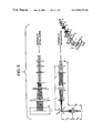
- FIG. 1 shows a schematic view of a laser annealing apparatus having used in the embodiments of the present invention
- FIG. 2 is a graph showing the relationship between the sheet resistance of a silicon film (phosphorus-doped, N-type) obtained by laser annealing according to an embodiment of the present invention and the applied laser energy density, while changing the repetition times of pulse shots;
- FIG. 3 is a graph showing the relationship between the sheet resistance of a silicon film (phosphorus- and boron-doped, P-type) obtained by laser annealing according to an embodiment of the present invention and the applied laser energy density, while changing the repetition times of pulse shots;
- FIG. 4 is a graph showing the relation between the morphology of the silicon film obtained in an embodiment or the present invention and the applied laser energy density and the repetition times of the pulse shots;
- FIG. 5 shows a concept of an optical system of the laser annealing apparatus having used in the embodiments of the present invention
- FIG. 6 shows a laser annealing process in accordance with the present invention.
- FIG. 7 shows another laser annealing process in accordance with the present invention.
- an impurity is introduced into a film comprising a Group IV element for imparting one of N-type conductivity and P-type conductivity thereto, and another impurity is introduced into a portion of the film with a mask for imparting the other one of the N-type conductivity and P-type conductivity to said portion.
- FIG. 1 is shown schematically a laser annealing apparatus having used in the present example.
- a laser beam is generated in a generator 2 , amplified in an amplifier 3 after traveling through full reflection mirrors 5 and 6 , and then introduced in an optical system 4 after passing through full reflection mirrors 7 and 8 .
- the initial laser beam has a rectangular beam area of about 3 ⁇ 2 cm 2 , but is processed into a long beam having a length of from about 10 to 30 cm and a width of from about 0.1 to 1 cm by the optical system 4 .
- the maximum energy of the laser having passed through this optical system was 1,000 mJ/shot.
- FIG. 5 An optical path in the optical system 4 is illustrated in FIG. 5.
- a laser light incident on the optical system 4 passes through a cylindrical concave lens A, a cylindrical convex lens B, a fly-eye lens C provided in a lateral direction and a fly-eye lens D provided in a vertical direction.
- the laser light is changed from an initial gauss distribution to a rectangular distribution by virtue of the fly-eye lenses C and D.
- the laser light passes through a cylindrical convex lenses E and F and is reflected on a mirror G (a mirror 9 in FIG. 1 ) and is focused on the specimen by a cylindrical lens H.
- a total length X 6 of the optical path is about 1.3 m.
- the initial beam is modified into a long-shaped one as above to improve processability thereof. More specifically, the in rectangular beam which is irradiated onto a specimen 11 through the full reflection mirror 9 after departing the optical system 4 has a longer width as compared with that of the specimen that, as a consequence, the specimen need to be moved only along one direction. Accordingly, the stage on which the specimen is mounted and the driving apparatus 10 can be made simple structured that the maintenance operation therefor can be easily conducted. Furthermore, the alignment operation at setting the specimen can also be greatly simplified.
- the specimen used in the example were various types of glass substrates (e.g., a Corning #7059 glass substrate) 100 mm in length and from 100 to 300 mm in width.
- a 100 nm thick amorphous silicon film was deposited on a glass substrate 61 by plasma assisted CVD (chemical vapor deposition) process.
- the resulting film was annealed at 600° C. for 48 hours to obtain a crystallized film, and was patterned to make island-like portions 62 and 63 (FIG. 6 (A)).
- a 70 nm thick silicon oxide film (a light-transmitting coating) 64 was deposited thereon by sputtering and the entire surface of the substrate was doped with phosphorus.
- a so-called ion doping process (FIG. 6 (B)) was employed in this step using phosphine (PH 3 ) as the plasma source and an accelerating voltage of 80 kV.
- a part of the substrate was masked 65 to implant boron by ion doping process (FIG. 6 (C)).
- Diborane (B 2 H 6 ) was used as the plasma source in this step while accelerating at a voltage of 65 kV.
- phosphorus was implanted (introduced) into the masked portions through the light-transmitting coating to obtain portion having rendered N-type conductive, while both phosphorus and boron were implanted (introduced) into the unmasked portions through the light-transmitting coating to result in a portion having rendered P-type conductive.
- FIG. 2 shows a graph which relates the sheet resistance of a silicon film having doped with phosphorus ions with the energy density of the laser beam while also changing the repetition of the pulse shots.
- Phosphorus was incorporated into the silicon film at a dose of 2 ⁇ 10 15 cm ⁇ 2 .
- a laser being operated at an energy density of 200 mJ/cm 2 or less, a large number of shots were necessary to activate the sheet, yet with a poor result yielding a high sheet resistance of about 10 k ⁇ /sq.
- a laser beam having an energy density of 200 mJ/cm 2 or higher a sufficient activation was realized with a laser operation of from 1 to 10 shots.
- FIG. 3 is shown the results for laser activating a silicon film doped with boron ions at a dose of 4 ⁇ 10 15 cm ⁇ 2 .
- activation could be conducted only insufficiently with an energy density of 200 mJ/cm 2 or lower that a large number of pulse shots was required for sufficient activation.
- a laser beam operated at an energy density of from 200 to 300 mJ/cm 2 a sufficiently low sheet resistance was obtained with 1 to 10 shots.
- the sheet resistance was reversely elevated.
- the laser annealing is applied simultaneously to both P- and N-type regions as shown in FIG. 6 (D).
- a laser beam being irradiated at an energy density of 350 mJ/cm 2 sufficiently activates the N-type region while impairing the properties of the P-type region.
- the laser beam is operated in an energy density range of from 200 to 300 mJ/cm 2 , and more preferably, in a range of from 250 to 300 mJ/cm 2 .
- the pulse repetition is preferably in the range of from 1 to 100 pulses.
- the morphology of the deposited film is considerably influenced by laser annealing.
- the number of pulse shots can be related to the laser beam energy density and the film morphology as illustrated in FIG. 4 .
- the term “Annealing Pulse” signifies the number of laser beam pulse shots.
- the solid circle in the figure represents the point at which a change in surface morphology was observed on a phosphorus-doped silicon, and the open circle represents the same on a boron-doped silicon.
- the upper region on the right hand side of the figure corresponds to a condition which yields poor morphology on the surface (rough surface), and the lower region on the left hand side of the figure corresponds to that which yields favorable morphology on the surface (smooth surface).
- the condition for conducting laser annealing without impairing the surface morphology can be read to be such which satisfies the relation: log 10 N ⁇ A ( E ⁇ B ), where, E (mJ/cm 2 ) is the energy density of the irradiated laser beam, and N (shots) is the number of shots of pulsed laser.
- the pulsed laser beam is shot at a frequency of 10 times or less. If the energy density is elevated to 280 mJ/cm 2 , the laser beam is preferably shot at a frequency of from 1 to 3 times. By conducting laser annealing under such conditions, the sheet resistance could be controlled within a fluctuation of 10% or less.
Abstract
A laser annealing process for recovering crystallinity of a deposited semiconductor film such as of silicon which had undergone morphological damage, said process comprising activating the semiconductor by irradiating a pulsed laser beam operating at a wavelength of 400 nm or less and at a pulse width of 50 nsec or less onto the surface of the film, wherein,
-
- said deposited film is coated with a transparent film such as a silicon oxide film at a thickness of from 3 to 300 nm, and the laser beam incident to said coating is applied at an energy density E (mJ/cm2) provided that it satisfies the relation:
log10 N≦−0.02 (E−350), - where N is the number of shots of the pulsed laser beam.
- said deposited film is coated with a transparent film such as a silicon oxide film at a thickness of from 3 to 300 nm, and the laser beam incident to said coating is applied at an energy density E (mJ/cm2) provided that it satisfies the relation:
Description
This application is a Divisional Application of application Ser. No. 08/709,108 filed Sep. 6, 1996, which is a continuation of application Ser. No. 08/409,929 filed Mar. 23, 1995 which is a continuation of application Ser. No. 08/081,696 filed Jun. 25, 1993.
1. Field of the Invention
The present invention relates to a highly reliable laser annealing process suited for use in mass production of semiconductor devices, which enables uniform annealing at high yield. More particularly, the present invention provides a laser annealing process of a deposited film whose crystallinity had been greatly impaired by the damage it had received through processes such as ion irradiation, ion implantation, and ion doping.
2. Prior Art
At present, methods of lowering of process temperatures in fabricating semiconductor devices are extensively studied. The reason for such an active research for low temperature processes owe partly to the need for fabricating semiconductor elements on an insulator substrate made of, e.g., glass. Laser annealing technology is regarded promising as the ultimate low temperature process.
However, conditions for laser annealing are not yet established because conventional laser annealing processes were each conducted independently under differing conditions which depend upon the apparatuses and the coating conditions chosen individually in each process. This has misled and has allowed many to think that the laser annealing technology fails to give results reliable and consistent enough to make the process practically feasible. An object of the present invention is to establish, for the first time, the conditions for a laser annealing process which yields highly reproducible results.
In a process for fabricating a semiconductor device, a deposition film is considerably damaged by processing such as ion irradiation, ion implantation, and ion doping, and is thereby impaired in crystallinity as to yield an amorphous phase or a like state which is far from being called as a semiconductor. Accordingly, with an aim to use laser annealing in activating such damaged films, the present inventors have studied extensively how to optimize the conditions of laser annealing. During the study, it has been found that the optimum condition fluctuates not only by the energy control of the laser beam, but also by the impurities being incorporated in the film and by the number of pulse shots of the laser beam being applied thereto.
The deposited films to be activated by the process of the present invention are those containing, as the principal component, a Group IV element of the periodic table, e.g., silicon, germanium, an alloy of silicon and germanium, or a compound of the Group IV element such as silicon carbide. The deposited film has a thickness of 100 Å to 10000 Å. By taking the light transmission into consideration, it is well established that the laser annealing of such films can be favorably conducted by applying a laser beam in the short wavelength region, and specifically, one of 400 nm or shorter.
The process of the present invention comprises the step of:
-
- irradiating laser pulses having a wavelength of 400 nm or shorter and having a pulse width of 50 nsec or less to a film comprising a Group IV element selected from the group consisting of carbon, silicon, germanium, tin and lead and having introduced thereinto an impurity ion,
- wherein a transparent film having a thickness of 3 to 300 nm is provided on said film comprising the Group IV element on the way of said laser pulses to said film comprising the Group IV element, an energy density E of each of said laser pulses in unit of mJ/cm2 and the number N of said laser pulses satisfy relation log10N≦−0.02(E−350).
The laser pulses are emitted from a laser selected from the group consisting of a KrF excimer laser, an ArF excimer laser, a XeCl excimer laser and a XeF excimer laser. The introduction of the impurity ion is carried out by ion irradiation, ion implantation or ion doping. The film comprising the Group IV element is provided on an insulating substrate, and the insulating substrate is maintained at a temperature of room temperature to 500° C. during the irradiating step.
It had been believed that the sheet resistance can be lowered by applying a laser beam having an energy density sufficiently high for activation. In the case of a film containing phosphorus as an impurity, this tendency can be certainly observed. However, in a film containing boron as an impurity, the film undergoes degradation by the irradiation of a laser of such a high energy density. Moreover, it had been taken for granted that the increase in pulsed shots reduces fluctuation in properties of the laser annealed films. However, this is not true because it was found that the morphology of the coating deteriorates with increasing number of shots to increase fluctuations in a microscopic level.
This can be explained by the growth of crystal nuclei within the coating due to a laser beam irradiation being applied repeatedly to the film. As a result, a grain size distribution within a size range of from 0.1 to 1 μm appears inside the coating which was previously composed of uniform sized grains. This phenomenon was particularly distinguished when a laser irradiation in the high energy region was applied.
It has been found that the deposited film (i.e. a semiconductor film) must be coated with (covered by) a light-transmitting coating from 3 to 300 nm in thickness instead of being exposed to atmosphere. The light-transmitting coating is preferably made from silicon oxide or silicon nitride from the viewpoint that it should transmit laser beam. More preferably, a material mainly comprising silicon oxide is used because, in general, it also serves as the gate dielectric. Needless to say, the light-transmitting film may be doped with phosphorus or boron with an aim to passivate the mobile ions. If the film containing a Group IV element should not be coated with such a light-transmitting coating, it happens that the uniformity is disturbed in a more accelerated manner.
It has been found also, that a further smoother (uniform) coating can be obtained by applying pulsed laser beam under a condition set forth above and additionally satisfying the following relation:
log10 N≦A(E−B)
where, E (mJ/cm2) is the energy density of each of the irradiated laser pulses, and N (shots) is the number of shots of pulsed laser. The values for A and B are dependent on the impurities being incorporated in the coating. When phosphorus is present as the impurity, −0.02 for A and 350 for B are chosen, and an A of −0.02 and B of 300 are selected when boron is included as the impurity.
Similar effect can be attained by using a transparent substrate instead of the transparent film. That is, a laser process in accordance with the present invention comprises the steps of:
-
- introducing an impurity into a semiconductor film provided on a transparent substrate; and
irradiating laser pulses having a wavelength of 400 nm or shorter and having a pulse width of 50 nsec or less to said semiconductor film through said transparent substrate,
-
- wherein an energy density E of each of said laser pulses in unit of mJ/cm2 and the number N of said laser pulses satisfy relation log10N≦−0.02(E−350).
FIG. 7(A) shows the introducing step, and FIG. 7(B) shows the irradiating step. Reference numeral 71 designates the transparent substrate, and 72 designates the semiconductor film.
The present invention is illustrated in greater detail referring to a non-limiting example below. It should be understood, however, that the present invention is not to be construed as being limited thereto.
In this EXAMPLE, an impurity is introduced into a film comprising a Group IV element for imparting one of N-type conductivity and P-type conductivity thereto, and another impurity is introduced into a portion of the film with a mask for imparting the other one of the N-type conductivity and P-type conductivity to said portion. In FIG. 1 is shown schematically a laser annealing apparatus having used in the present example. A laser beam is generated in a generator 2, amplified in an amplifier 3 after traveling through full reflection mirrors 5 and 6, and then introduced in an optical system 4 after passing through full reflection mirrors 7 and 8. The initial laser beam has a rectangular beam area of about 3×2 cm2, but is processed into a long beam having a length of from about 10 to 30 cm and a width of from about 0.1 to 1 cm by the optical system 4. The maximum energy of the laser having passed through this optical system was 1,000 mJ/shot.
An optical path in the optical system 4 is illustrated in FIG. 5. A laser light incident on the optical system 4 passes through a cylindrical concave lens A, a cylindrical convex lens B, a fly-eye lens C provided in a lateral direction and a fly-eye lens D provided in a vertical direction. The laser light is changed from an initial gauss distribution to a rectangular distribution by virtue of the fly-eye lenses C and D. Further, the laser light passes through a cylindrical convex lenses E and F and is reflected on a mirror G (a mirror 9 in FIG. 1 ) and is focused on the specimen by a cylindrical lens H.
In this EXAMPLE, distances X1 and X2 indicated in FIG. 5 are fixed, and a distance X3 between a virtual focus I (which is generated by the difference between curved surfaces of the fly-eye lenses) and the mirror G, distances X4 and X5 are varied to adjust a magnification M and a focal length F. That is,
M=(X 3 +X 4)/X 5
1/F=1/(X 3 +X 4)+1/X 5.
M=(X 3 +X 4)/X 5
1/F=1/(X 3 +X 4)+1/X 5.
In this EXAMPLE, a total length X6 of the optical path is about 1.3 m.
The initial beam is modified into a long-shaped one as above to improve processability thereof. More specifically, the in rectangular beam which is irradiated onto a specimen 11 through the full reflection mirror 9 after departing the optical system 4 has a longer width as compared with that of the specimen that, as a consequence, the specimen need to be moved only along one direction. Accordingly, the stage on which the specimen is mounted and the driving apparatus 10 can be made simple structured that the maintenance operation therefor can be easily conducted. Furthermore, the alignment operation at setting the specimen can also be greatly simplified.
If a beam having a square cross section were to be employed, on the other hand, it becomes impossible to cover the entire substrate with a single beam. Accordingly, the specimen should be moved two dimensionally along two directions. In such circumstances, however, the driving apparatus of the stage becomes complicated and the alignment also must be done in a two dimensional manner that it involves much difficulty. When the alignment is done manually, in particular, a considerable time is consumed for this step to greatly reduce the productivity of the entire process. Furthermore, those apparatuses must be fixed on a stable table 1 such as a vibration proof table.
The specimen used in the example were various types of glass substrates (e.g., a Corning #7059 glass substrate) 100 mm in length and from 100 to 300 mm in width. A KrF laser emitting light at a wavelength of 248 nm and at a pulse width of 50 nsec or less, e.g. 30 nsec, was used in the process.
A 100 nm thick amorphous silicon film was deposited on a glass substrate 61 by plasma assisted CVD (chemical vapor deposition) process. The resulting film was annealed at 600° C. for 48 hours to obtain a crystallized film, and was patterned to make island-like portions 62 and 63 (FIG. 6(A)). Furthermore, a 70 nm thick silicon oxide film (a light-transmitting coating) 64 was deposited thereon by sputtering and the entire surface of the substrate was doped with phosphorus. A so-called ion doping process (FIG. 6(B)) was employed in this step using phosphine (PH3) as the plasma source and an accelerating voltage of 80 kV. Furthermore, a part of the substrate was masked 65 to implant boron by ion doping process (FIG. 6(C)). Diborane (B2H6) was used as the plasma source in this step while accelerating at a voltage of 65 kV. More specifically, phosphorus was implanted (introduced) into the masked portions through the light-transmitting coating to obtain portion having rendered N-type conductive, while both phosphorus and boron were implanted (introduced) into the unmasked portions through the light-transmitting coating to result in a portion having rendered P-type conductive.
Then, laser beam was irradiated to the island-like portions (semiconductor film) while varying the energy density and the number of pulse shots to effect laser activation. The sheet resistance was measured accordingly and the morphology of the crystallites constituting the coating was observed through an optical microscope. The results are summarized in FIGS. 2 to 4.
In FIG. 3 is shown the results for laser activating a silicon film doped with boron ions at a dose of 4×1015 cm−2. In this case again, activation could be conducted only insufficiently with an energy density of 200 mJ/cm2 or lower that a large number of pulse shots was required for sufficient activation. With a laser beam operated at an energy density of from 200 to 300 mJ/cm2, a sufficiently low sheet resistance was obtained with 1 to 10 shots. However, with laser being operated at an energy density of 300 mJ/cm2 or higher, on the other hand, the sheet resistance was reversely elevated. In particular, contrary to the case of activating with a laser beam energy density of 200 mJ/cm2 or lower, the sheet resistance was elevated with increasing repetition of pulse shots. This phenomenon can be explained by the growth of grain boundary due to the impaired homogeneity of the film which had resulted by applying laser irradiation for too many shots.
In a practical process, the laser annealing is applied simultaneously to both P- and N-type regions as shown in FIG. 6(D). This signifies that a laser beam being irradiated at an energy density of 350 mJ/cm2 sufficiently activates the N-type region while impairing the properties of the P-type region. Accordingly, in the process according to the present example, it is preferred that the laser beam is operated in an energy density range of from 200 to 300 mJ/cm2, and more preferably, in a range of from 250 to 300 mJ/cm2. The pulse repetition is preferably in the range of from 1 to 100 pulses.
As described in the foregoing, the morphology of the deposited film is considerably influenced by laser annealing. In fact, the number of pulse shots can be related to the laser beam energy density and the film morphology as illustrated in FIG. 4. In FIG. 4 , the term “Annealing Pulse” signifies the number of laser beam pulse shots. The solid circle in the figure represents the point at which a change in surface morphology was observed on a phosphorus-doped silicon, and the open circle represents the same on a boron-doped silicon. The upper region on the right hand side of the figure corresponds to a condition which yields poor morphology on the surface (rough surface), and the lower region on the left hand side of the figure corresponds to that which yields favorable morphology on the surface (smooth surface). It can be seen from the results that the phosphorus-doped silicon has a strong resistance against laser irradiation. Accordingly, the condition for conducting laser annealing without impairing the surface morphology can be read to be such which satisfies the relation:
log10 N≦A(E−B),
where, E (mJ/cm2) is the energy density of the irradiated laser beam, and N (shots) is the number of shots of pulsed laser. The values for A and B are A=−0.02 and B=350 in the case phosphorus is incorporated as the impurity, and are A=−0.02 and B=300 when boron is included as the impurity.
When the morphology of the deposited film is considerably impaired, the characteristic values show large scattering due to the serious drop which occurs locally in the properties of silicon. In fact, a scattering in sheet resistance as high as 20% or even more was observed on a silicon film having a defective morphology (a rough surface). This scattering can be removed by satisfying the conditions above and by setting the laser energy density at a pertinent value.
For instance, when a laser energy density is set at 250 mJ/cm2, the pulsed laser beam is shot at a frequency of 10 times or less. If the energy density is elevated to 280 mJ/cm2, the laser beam is preferably shot at a frequency of from 1 to 3 times. By conducting laser annealing under such conditions, the sheet resistance could be controlled within a fluctuation of 10% or less.
According to the present invention, a highly reliable semiconductor film having low fluctuation in properties was obtained by setting the optimal conditions for laser annealing as described in the foregoing. It can be seen therefore that the process according to the present invention is beneficial to the semiconductor industry.
While the invention has been described in detail and with reference to specific embodiments thereof, it will be apparent to one skilled in the art that various changes and modifications can be made therein without departing from the spirit and scope thereof.
Claims (26)
1. A method of manufacturing a semiconductor device comprising the steps of:
preparing a plurality of semiconductor islands over a glass substrate;
subjecting said semiconductor islands to an ion doping;
directing a pulsed laser beam having a cross section elongated in one direction to said glass substrate;
moving said glass substrate in a direction perpendicular to the elongation direction of said pulsed laser beam during directing said pulsed laser beam to said glass substrate, thereby irradiating said semiconductor islands with said pulsed laser beam.
2. A method according to claim 1 wherein an energy density of said pulsed laser beam is not higher than 300 mJ/cm2.
3. A method according to claim 1 wherein an impurity selected from the group consisting of phosphorus and boron is selectively introduced into said plurality of semiconductor islands by said ion doping.
4. A method according to claim 1 wherein each of said semiconductor islands is irradiated with plural pulses of said pulsed laser beam.
5. A method of manufacmrfing a semiconductor device comprising the steps of:
forming a semiconductor film over a glass substrate;
crystallizing said semiconductor film;
patterning the crystallized semiconductor film into a plurality of semiconductor islands;
subjecting said semiconductor islands to an ion doping;
directing a pulsed laser beam having a cross section elongated in one direction to said glass substrate;
moving said glass substrate in a direction perpendicular to the elongation direction of said pulsed laser beam during directing said pulsed laser beam to said sass substrate, thereby irradiating said semiconductor islands with said pulsed laser beam.
6. A method according to claim 5 wherein an energy density of said pulsed laser beam is not higher than 300 mJ/cm2.
7. A method according to claim 5 wherein an impurity selected from the group consisting of phosphorus and boron is selectively introduced into said plurality of semiconductor islands by said ion doping.
8. A method according to claim 5 wherein each of said semiconductor islands is irradiated with plural pulses of said pulsed laser beam.
9. A method of manufacturing a semiconductor device comprising the steps of:
preparing a plurality of first semiconductor islands and a plurality of second semiconductor islands over a glass substrate;
subjecting both of said first and second semiconductor islands to a first ion doping for introducing a first impurity;
subjecting only said first semiconductor islands to a second ion doping for introducing a second impurity wherein said second impurity has an opposite conductivity type to said first impurity;
directing a pulsed laser beam having a cross section elongated in one direction to said glass substrate;
moving said glass substrate in a direction perpendicular to the elongation direction of said pulsed laser beam during directing said pulsed laser beam to said glass substrate, thereby irradiating both of said first and second semiconductor islands with said pulsed laser beam.
10. A method according to claim 9 wherein an energy density of said pulsed laser beam is not higher than 300 mJ/cm2.
11. A method according to claim 9 wherein said first impurity is phosphorus while said second impurity is boron.
12. A method according to claim 9 wherein each of said first and second semiconductor islands is irradiated with plural pulses of said pulsed laser beam.
13. A method of manufacturing a semiconductor device comprising the steps of:
preparing a plurality of semiconductor islands over a glass substrate;
forming a film comprising silicon oxide over said glass substrate wherein said semiconductor islands are covered by said film;
subjecting said semiconductor islands to an ion doping through said film;
directing a pulsed laser beam having a cross section elongated in one direction to said glass substrate;
moving said glass substrate in a direction perpendicular to the elongation direction of said pulsed laser bean during directing said pulsed laser beam to said glass substrate, thereby irradiating said semiconductor islands with said pulsed laser beam through said film.
14. A method according to claim 13 wherein an energy density of said pulsed laser beam is not higher than 300 mJ/cm2.
15. A method according to claim 13 wherein an impurity selected from the group consisting of phosphorus and boron is selectively introduced into said plurality of semiconductor islands by said ion doping.
16. A method according to claim 13 wherein each of said semiconductor islands is irradiated with plural pulses of said pulsed laser beam.
17. A method of manufacturing a semiconductor device comprising the steps of:
preparing a plurality of semiconductor islands comprising silicon and germanium over a substrate;
subjecting said semiconductor islands to an ion doping;
directing a pulsed laser beam having a cross section elongated in one direction to said glass substrate;
moving said glass substrate in a direction perpendicular to the elongation direction of said pulsed laser beam during directing said pulsed laser beam to said glass substrate, thereby irradiating said semiconductor islands with said pulsed laser beam.
18. A method according to claim 17 wherein an impurity selected from the group consisting of phosphorus and boron is selectively introduced into said plurality of semiconductor islands by said ion doping.
19. A method of manufacturing a semiconductor device comprising the steps of:
preparing a plurality of semiconductor islands comprising silicon and germanium over a substrate;
forming a film comprising silicon oxide over said glass substrate wherein said semiconductor islands are covered by said film;
subjecting said semiconductor islands to an ion doping through said film;
directing a pulsed laser beam having a cross section elongated in one direction to said glass substrate;
moving said glass substrate in a direction perpendicular to the elongation direction of said pulsed laser beam during directing said pulsed laser beam to said glass substrate, thereby irradiating said semiconductor islands with said pulsed laser beam through said film.
20. The method of manufacturing a semiconductor device according to claim 19 wherein each of said semiconductor islands is irradiated with plural pulses of said pulsed excimer laser beam.
21. The method of claim 1 , wherein said pulsed laser beam is a pulsed excimer laser beam.
22. The method of claim 5 , wherein said pulsed laser beam is a pulsed excimer laser beam.
23. The method of claim 9 , wherein said pulsed laser beam is a pulsed excimer laser beam.
24. The method of claim 13 , wherein said pulsed laser beam is a pulsed excimer laser beam.
25. The method of claim 17 , wherein said pulsed laser beam is a pulsed excimer laser beam.
26. The method of claim 19 , wherein said pulsed laser beam is a pulsed excimer laser beam.
Priority Applications (2)
| Application Number | Priority Date | Filing Date | Title |
|---|---|---|---|
| US09/197,534 US6991975B1 (en) | 1992-06-26 | 1998-11-23 | Laser process |
| US11/321,641 US7985635B2 (en) | 1992-06-26 | 2005-12-30 | Laser process |
Applications Claiming Priority (6)
| Application Number | Priority Date | Filing Date | Title |
|---|---|---|---|
| JP19300592 | 1992-06-26 | ||
| JP25229592 | 1992-08-27 | ||
| US8169693A | 1993-06-25 | 1993-06-25 | |
| US40992995A | 1995-03-23 | 1995-03-23 | |
| US08/709,108 US5858473A (en) | 1992-06-26 | 1996-09-06 | Laser process |
| US09/197,534 US6991975B1 (en) | 1992-06-26 | 1998-11-23 | Laser process |
Related Parent Applications (2)
| Application Number | Title | Priority Date | Filing Date |
|---|---|---|---|
| US40992995A Continuation | 1992-06-26 | 1995-03-23 | |
| US08/709,108 Division US5858473A (en) | 1992-06-26 | 1996-09-06 | Laser process |
Related Child Applications (1)
| Application Number | Title | Priority Date | Filing Date |
|---|---|---|---|
| US11/321,641 Division US7985635B2 (en) | 1992-06-26 | 2005-12-30 | Laser process |
Publications (1)
| Publication Number | Publication Date |
|---|---|
| US6991975B1 true US6991975B1 (en) | 2006-01-31 |
Family
ID=26507640
Family Applications (7)
| Application Number | Title | Priority Date | Filing Date |
|---|---|---|---|
| US08/661,869 Expired - Lifetime US5897799A (en) | 1992-06-26 | 1996-06-11 | Laser processing apparatus |
| US08/709,108 Expired - Lifetime US5858473A (en) | 1992-06-26 | 1996-09-06 | Laser process |
| US08/956,438 Expired - Lifetime US6002101A (en) | 1992-06-26 | 1997-10-23 | Method of manufacturing a semiconductor device by using a homogenized rectangular laser beam |
| US08/956,439 Expired - Lifetime US5968383A (en) | 1992-06-26 | 1997-10-23 | Laser processing apparatus having beam expander |
| US09/197,534 Expired - Fee Related US6991975B1 (en) | 1992-06-26 | 1998-11-23 | Laser process |
| US09/351,159 Expired - Fee Related US6440785B1 (en) | 1992-06-26 | 1999-07-12 | Method of manufacturing a semiconductor device utilizing a laser annealing process |
| US11/321,641 Expired - Fee Related US7985635B2 (en) | 1992-06-26 | 2005-12-30 | Laser process |
Family Applications Before (4)
| Application Number | Title | Priority Date | Filing Date |
|---|---|---|---|
| US08/661,869 Expired - Lifetime US5897799A (en) | 1992-06-26 | 1996-06-11 | Laser processing apparatus |
| US08/709,108 Expired - Lifetime US5858473A (en) | 1992-06-26 | 1996-09-06 | Laser process |
| US08/956,438 Expired - Lifetime US6002101A (en) | 1992-06-26 | 1997-10-23 | Method of manufacturing a semiconductor device by using a homogenized rectangular laser beam |
| US08/956,439 Expired - Lifetime US5968383A (en) | 1992-06-26 | 1997-10-23 | Laser processing apparatus having beam expander |
Family Applications After (2)
| Application Number | Title | Priority Date | Filing Date |
|---|---|---|---|
| US09/351,159 Expired - Fee Related US6440785B1 (en) | 1992-06-26 | 1999-07-12 | Method of manufacturing a semiconductor device utilizing a laser annealing process |
| US11/321,641 Expired - Fee Related US7985635B2 (en) | 1992-06-26 | 2005-12-30 | Laser process |
Country Status (4)
| Country | Link |
|---|---|
| US (7) | US5897799A (en) |
| JP (10) | JPH06124913A (en) |
| KR (6) | KR970005141B1 (en) |
| CN (7) | CN1921069B (en) |
Cited By (3)
| Publication number | Priority date | Publication date | Assignee | Title |
|---|---|---|---|---|
| US20030060026A1 (en) * | 1995-07-25 | 2003-03-27 | Semiconductor Energy Laboratory Co. Ltd., A Japanese Corporation | Laser annealing method and apparatus |
| US20070091978A1 (en) * | 2005-10-26 | 2007-04-26 | Semiconductor Energy Laboratory Co. Ltd. | Laser irradiation apparatus and manufacturing method of semiconductor device |
| RU2486282C1 (en) * | 2011-11-17 | 2013-06-27 | Федеральное государственное автономное образовательное учреждение высшего профессионального образования "Уральский федеральный университет имени первого Президента России Б.Н. Ельцина" | Method of producing quartz glass implanted with tin ions |
Families Citing this family (103)
| Publication number | Priority date | Publication date | Assignee | Title |
|---|---|---|---|---|
| US6149988A (en) * | 1986-09-26 | 2000-11-21 | Semiconductor Energy Laboratory Co., Ltd. | Method and system of laser processing |
| US6261856B1 (en) * | 1987-09-16 | 2001-07-17 | Semiconductor Energy Laboratory Co., Ltd. | Method and system of laser processing |
| JPH06124913A (en) | 1992-06-26 | 1994-05-06 | Semiconductor Energy Lab Co Ltd | Laser treatment |
| US5643801A (en) * | 1992-11-06 | 1997-07-01 | Semiconductor Energy Laboratory Co., Ltd. | Laser processing method and alignment |
| CN1052566C (en) | 1993-11-05 | 2000-05-17 | 株式会社半导体能源研究所 | Method for processing semiconductor device, apparatus for processing a semiconductor and apparatus for processing semiconductor device |
| US6897100B2 (en) | 1993-11-05 | 2005-05-24 | Semiconductor Energy Laboratory Co., Ltd. | Method for processing semiconductor device apparatus for processing a semiconductor and apparatus for processing semiconductor device |
| KR100321541B1 (en) | 1994-03-09 | 2002-06-20 | 야마자끼 순페이 | How Active Matrix Display Devices Work |
| US6723590B1 (en) | 1994-03-09 | 2004-04-20 | Semiconductor Energy Laboratory Co., Ltd. | Method for laser-processing semiconductor device |
| US6300176B1 (en) * | 1994-07-22 | 2001-10-09 | Semiconductor Energy Laboratory Co., Ltd. | Laser processing method |
| JP3469337B2 (en) | 1994-12-16 | 2003-11-25 | 株式会社半導体エネルギー研究所 | Method for manufacturing semiconductor device |
| US6130120A (en) | 1995-01-03 | 2000-10-10 | Goldstar Electron Co., Ltd. | Method and structure for crystallizing a film |
| US5854803A (en) * | 1995-01-12 | 1998-12-29 | Semiconductor Energy Laboratory Co., Ltd. | Laser illumination system |
| TW305063B (en) * | 1995-02-02 | 1997-05-11 | Handotai Energy Kenkyusho Kk | |
| TW297138B (en) * | 1995-05-31 | 1997-02-01 | Handotai Energy Kenkyusho Kk | |
| JP2007251196A (en) * | 1995-07-25 | 2007-09-27 | Semiconductor Energy Lab Co Ltd | Manufacturing method of laser beam irradiation device and semiconductor device |
| JP3917231B2 (en) | 1996-02-06 | 2007-05-23 | 株式会社半導体エネルギー研究所 | Laser irradiation apparatus and laser irradiation method |
| US6599790B1 (en) | 1996-02-15 | 2003-07-29 | Semiconductor Energy Laboratory Co., Ltd | Laser-irradiation method and laser-irradiation device |
| JPH09234579A (en) * | 1996-02-28 | 1997-09-09 | Semiconductor Energy Lab Co Ltd | Laser beam irradiating device |
| US6759628B1 (en) * | 1996-06-20 | 2004-07-06 | Sony Corporation | Laser annealing apparatus |
| US6040019A (en) * | 1997-02-14 | 2000-03-21 | Advanced Micro Devices, Inc. | Method of selectively annealing damaged doped regions |
| JPH10253916A (en) * | 1997-03-10 | 1998-09-25 | Semiconductor Energy Lab Co Ltd | Laser optical device |
| JP3770999B2 (en) * | 1997-04-21 | 2006-04-26 | 株式会社半導体エネルギー研究所 | Laser irradiation apparatus and laser irradiation method |
| JP3462053B2 (en) * | 1997-09-30 | 2003-11-05 | 株式会社半導体エネルギー研究所 | Beam homogenizer, laser irradiation apparatus, laser irradiation method, and semiconductor device |
| JPH11186189A (en) * | 1997-12-17 | 1999-07-09 | Semiconductor Energy Lab Co Ltd | Laser irradiation equipment |
| JP4663047B2 (en) | 1998-07-13 | 2011-03-30 | 株式会社半導体エネルギー研究所 | Laser irradiation apparatus and method for manufacturing semiconductor device |
| US6246524B1 (en) | 1998-07-13 | 2001-06-12 | Semiconductor Energy Laboratory Co., Ltd. | Beam homogenizer, laser irradiation apparatus, laser irradiation method, and method of manufacturing semiconductor device |
| KR100430231B1 (en) * | 1998-10-02 | 2004-07-19 | 엘지.필립스 엘시디 주식회사 | Laser Annealing Equipment |
| EP1744349A3 (en) | 1998-10-05 | 2007-04-04 | Semiconductor Energy Laboratory Co., Ltd. | Laser irradiation apparatus, laser irradiation method, beam homogenizer, semiconductor device, and method of manufacturing the semiconductor device |
| US6204160B1 (en) * | 1999-02-22 | 2001-03-20 | The United States Of America As Represented By The Secretary Of The Navy | Method for making electrical contacts and junctions in silicon carbide |
| US6393042B1 (en) | 1999-03-08 | 2002-05-21 | Semiconductor Energy Laboratory Co., Ltd. | Beam homogenizer and laser irradiation apparatus |
| JP3562389B2 (en) * | 1999-06-25 | 2004-09-08 | 三菱電機株式会社 | Laser heat treatment equipment |
| JP4827276B2 (en) | 1999-07-05 | 2011-11-30 | 株式会社半導体エネルギー研究所 | Laser irradiation apparatus, laser irradiation method, and manufacturing method of semiconductor device |
| US6567219B1 (en) * | 1999-08-13 | 2003-05-20 | Semiconductor Energy Laboratory Co., Ltd. | Laser irradiation apparatus |
| US7160765B2 (en) * | 1999-08-13 | 2007-01-09 | Semiconductor Energy Laboratory Co., Ltd. | Method for manufacturing a semiconductor device |
| TW544727B (en) * | 1999-08-13 | 2003-08-01 | Semiconductor Energy Lab | Method of manufacturing a semiconductor device |
| TW494444B (en) * | 1999-08-18 | 2002-07-11 | Semiconductor Energy Lab | Laser apparatus and laser annealing method |
| US6548370B1 (en) | 1999-08-18 | 2003-04-15 | Semiconductor Energy Laboratory Co., Ltd. | Method of crystallizing a semiconductor layer by applying laser irradiation that vary in energy to its top and bottom surfaces |
| KR100319455B1 (en) | 1999-12-24 | 2002-01-05 | 오길록 | Optics system for crystallization tool |
| US6872607B2 (en) * | 2000-03-21 | 2005-03-29 | Semiconductor Energy Laboratory Co., Ltd. | Method of manufacturing a semiconductor device |
| US7078321B2 (en) | 2000-06-19 | 2006-07-18 | Semiconductor Energy Laboratory Co., Ltd. | Semiconductor device and method of manufacturing the same |
| TW523791B (en) * | 2000-09-01 | 2003-03-11 | Semiconductor Energy Lab | Method of processing beam, laser irradiation apparatus, and method of manufacturing semiconductor device |
| TW528879B (en) * | 2001-02-22 | 2003-04-21 | Ishikawajima Harima Heavy Ind | Illumination optical system and laser processor having the same |
| JP4921643B2 (en) * | 2001-02-22 | 2012-04-25 | 株式会社Ihi | Illumination optical system and laser processing apparatus including the same |
| US7061959B2 (en) * | 2001-04-18 | 2006-06-13 | Tcz Gmbh | Laser thin film poly-silicon annealing system |
| US7009140B2 (en) * | 2001-04-18 | 2006-03-07 | Cymer, Inc. | Laser thin film poly-silicon annealing optical system |
| TW558861B (en) * | 2001-06-15 | 2003-10-21 | Semiconductor Energy Lab | Laser irradiation stage, laser irradiation optical system, laser irradiation apparatus, laser irradiation method, and method of manufacturing semiconductor device |
| TW552645B (en) * | 2001-08-03 | 2003-09-11 | Semiconductor Energy Lab | Laser irradiating device, laser irradiating method and manufacturing method of semiconductor device |
| US7372630B2 (en) * | 2001-08-17 | 2008-05-13 | Semiconductor Energy Laboratory Co., Ltd. | Laser, irradiation apparatus, laser irradiation method, and method for manufacturing semiconductor device |
| CN2546122Y (en) * | 2001-11-20 | 2003-04-23 | 青岛迪玛特五金工具有限公司 | Laser locating system for hole working machinery |
| US6937336B2 (en) * | 2002-08-15 | 2005-08-30 | Black & Decker, Inc. | Optical alignment system for power tool |
| US8004664B2 (en) | 2002-04-18 | 2011-08-23 | Chang Type Industrial Company | Power tool control system |
| KR20030095313A (en) * | 2002-06-07 | 2003-12-18 | 후지 샤신 필름 가부시기가이샤 | Laser annealer and laser thin-film forming apparatus |
| US20030233921A1 (en) | 2002-06-19 | 2003-12-25 | Garcia Jaime E. | Cutter with optical alignment system |
| JP2004128421A (en) * | 2002-10-07 | 2004-04-22 | Semiconductor Energy Lab Co Ltd | Laser irradiation method, laser irradiation device, and method for manufacturing semiconductor device |
| JP4429586B2 (en) * | 2002-11-08 | 2010-03-10 | 株式会社半導体エネルギー研究所 | Method for manufacturing semiconductor device |
| US7160762B2 (en) * | 2002-11-08 | 2007-01-09 | Semiconductor Energy Laboratory Co., Ltd. | Method for manufacturing semiconductor device, semiconductor device, and laser irradiation apparatus |
| SG129265A1 (en) * | 2002-11-29 | 2007-02-26 | Semiconductor Energy Lab | Laser irradiation apparatus, laser irradiation method, and method for manufacturing a semiconductor device |
| US7056810B2 (en) * | 2002-12-18 | 2006-06-06 | Semiconductor Energy Laboratory Co., Ltd. | Method for manufacturing semiconductor apparatus, and semiconductor apparatus and electric appliance |
| JP4515034B2 (en) | 2003-02-28 | 2010-07-28 | 株式会社半導体エネルギー研究所 | Method for manufacturing semiconductor device |
| DE602004020538D1 (en) * | 2003-02-28 | 2009-05-28 | Semiconductor Energy Lab | Method and device for laser irradiation, and method for the production of semiconductors. |
| US7524712B2 (en) * | 2003-03-07 | 2009-04-28 | Semiconductor Energy Laboratory Co., Ltd. | Method for manufacturing a semiconductor device and laser irradiation method and laser irradiation apparatus |
| US7304005B2 (en) | 2003-03-17 | 2007-12-04 | Semiconductor Energy Laboratory Co., Ltd. | Laser irradiation apparatus, laser irradiation method, and method for manufacturing a semiconductor device |
| JP4373115B2 (en) * | 2003-04-04 | 2009-11-25 | 株式会社半導体エネルギー研究所 | Method for manufacturing semiconductor device |
| US7210820B2 (en) * | 2003-05-07 | 2007-05-01 | Resonetics, Inc. | Methods and apparatuses for homogenizing light |
| US7208395B2 (en) * | 2003-06-26 | 2007-04-24 | Semiconductor Energy Laboratory Co., Ltd. | Laser irradiation apparatus, laser irradiation method, and method for manufacturing semiconductor device |
| US7336907B2 (en) * | 2003-10-31 | 2008-02-26 | Texas Instruments Incorporated | Optical assembly having cylindrical lenses and related method of modulating optical signals |
| CN100571959C (en) * | 2003-11-26 | 2009-12-23 | Tcz私营有限公司 | Laser thin film poly-silicon annealing optical system |
| JP4342429B2 (en) * | 2004-02-09 | 2009-10-14 | 株式会社東芝 | Manufacturing method of semiconductor device |
| US20060146906A1 (en) * | 2004-02-18 | 2006-07-06 | Cymer, Inc. | LLP EUV drive laser |
| JP4579575B2 (en) * | 2004-05-14 | 2010-11-10 | 株式会社半導体エネルギー研究所 | Laser irradiation method and laser irradiation apparatus |
| JP5132119B2 (en) * | 2005-10-26 | 2013-01-30 | 株式会社半導体エネルギー研究所 | Method for manufacturing semiconductor device |
| US7679029B2 (en) | 2005-10-28 | 2010-03-16 | Cymer, Inc. | Systems and methods to shape laser light as a line beam for interaction with a substrate having surface variations |
| US20070117287A1 (en) * | 2005-11-23 | 2007-05-24 | Semiconductor Energy Laboratory Co., Ltd. | Laser irradiation apparatus |
| CN101346800B (en) * | 2005-12-20 | 2011-09-14 | 株式会社半导体能源研究所 | Laser irradiation apparatus and method for manufacturing semiconductor device |
| US7307237B2 (en) * | 2005-12-29 | 2007-12-11 | Honeywell International, Inc. | Hand-held laser welding wand nozzle assembly including laser and feeder extension tips |
| JP2008124149A (en) | 2006-11-09 | 2008-05-29 | Advanced Lcd Technologies Development Center Co Ltd | Optical device, and crystallization equipment |
| DE102007036262A1 (en) * | 2007-08-02 | 2009-02-05 | Robert Bosch Gmbh | Radar sensor for motor vehicles |
| JP2009283807A (en) * | 2008-05-26 | 2009-12-03 | Canon Inc | Structure including nitride semiconductor layer, composite substrate including nitride semiconductor layer, and method for manufacturing them |
| JP5414467B2 (en) * | 2009-11-09 | 2014-02-12 | キヤノン株式会社 | Laser processing method |
| US9069255B2 (en) * | 2009-11-18 | 2015-06-30 | Jim Hennessy | Carrier sheet for a photosensitive printing element |
| JP5302937B2 (en) * | 2010-07-20 | 2013-10-02 | 株式会社イー・エム・ディー | Impurity activation method, semiconductor device manufacturing method |
| CN102169816B (en) * | 2011-03-09 | 2013-02-27 | 清华大学 | Shielding electrode device in ultra-shallow junction deep ultraviolet laser annealing apparatus |
| GB2490143B (en) * | 2011-04-20 | 2013-03-13 | Rolls Royce Plc | Method of manufacturing a component |
| DE102011002236A1 (en) * | 2011-04-21 | 2012-10-25 | Dritte Patentportfolio Beteiligungsgesellschaft Mbh & Co.Kg | Process for producing a polycrystalline layer |
| US9769902B1 (en) | 2011-05-09 | 2017-09-19 | The United States Of America As Represented By Secretary Of The Air Force | Laser sensor stimulator |
| US9859348B2 (en) | 2011-10-14 | 2018-01-02 | Diftek Lasers, Inc. | Electronic device and method of making thereof |
| JP5920662B2 (en) * | 2012-06-05 | 2016-05-18 | 三菱マテリアル株式会社 | Laser processing apparatus and laser processing method |
| JP5920661B2 (en) * | 2012-06-05 | 2016-05-18 | 三菱マテリアル株式会社 | Laser processing apparatus and laser processing method |
| WO2014005755A1 (en) | 2012-07-04 | 2014-01-09 | Saint-Gobain Glass France | Device and method for laser processing of large-area substrates using at least two bridges |
| DE102015000449A1 (en) | 2015-01-15 | 2016-07-21 | Siltectra Gmbh | Solid body distribution by means of material conversion |
| EP2953158A3 (en) | 2014-06-04 | 2016-02-17 | Diftek Lasers, Inc. | Method of fabricating crystalline island on substrate |
| US10121667B2 (en) | 2014-11-12 | 2018-11-06 | President And Fellows Of Harvard College | Creation of hyperdoped semiconductors with concurrent high crystallinity and high sub-bandgap absorptance using nanosecond laser annealing |
| EP4234156A3 (en) | 2014-11-27 | 2023-10-11 | Siltectra GmbH | Laser based slicing method |
| KR20230145246A (en) | 2014-11-27 | 2023-10-17 | 실텍트라 게엠베하 | Splitting of a solid using conversion of material |
| FR3035540B1 (en) * | 2015-04-27 | 2017-04-28 | Centre Nat Rech Scient | PRINTING METHOD USING TWO LASERS |
| US10312310B2 (en) | 2016-01-19 | 2019-06-04 | Diftek Lasers, Inc. | OLED display and method of fabrication thereof |
| CN106024604B (en) * | 2016-08-02 | 2018-11-23 | 京东方科技集团股份有限公司 | A kind of laser annealing apparatus |
| JP6870286B2 (en) * | 2016-11-15 | 2021-05-12 | 富士電機株式会社 | Manufacturing method of silicon carbide semiconductor device |
| US9933592B1 (en) | 2017-01-20 | 2018-04-03 | Bae Systems Information And Electronic Systems Integration Inc. | Large aperture, passive optical athermalized beam expander for eye-safe lasers |
| CN106903424B (en) * | 2017-02-20 | 2018-05-29 | 温州大学激光与光电智能制造研究院 | A kind of post-processing approach that optical element mechanical property is improved based on laser blast wave |
| US10411027B2 (en) | 2017-10-19 | 2019-09-10 | Globalfoundries Singapore Pte. Ltd. | Integrated circuits with memory cells and method for producing the same |
| CN109095587B (en) * | 2018-08-28 | 2021-08-03 | 江苏大学 | Optical device based on cavitation degradation waste water |
| CN111843713A (en) * | 2020-06-29 | 2020-10-30 | 江苏亚威艾欧斯激光科技有限公司 | Lens processing device and lens array |
Citations (72)
| Publication number | Priority date | Publication date | Assignee | Title |
|---|---|---|---|---|
| US4059461A (en) | 1975-12-10 | 1977-11-22 | Massachusetts Institute Of Technology | Method for improving the crystallinity of semiconductor films by laser beam scanning and the products thereof |
| US4151008A (en) | 1974-11-15 | 1979-04-24 | Spire Corporation | Method involving pulsed light processing of semiconductor devices |
| JPS5532026A (en) | 1978-08-25 | 1980-03-06 | Seiko Epson Corp | Liquid crystal display panel |
| US4198246A (en) | 1978-11-27 | 1980-04-15 | Rca Corporation | Pulsed laser irradiation for reducing resistivity of a doped polycrystalline silicon film |
| US4262208A (en) | 1977-05-01 | 1981-04-14 | Canon Kabushiki Kaisha | Photo-electrical detecting apparatus |
| US4309224A (en) | 1978-10-06 | 1982-01-05 | Tokyo Shibaura Denki Kabushiki Kaisha | Method for manufacturing a semiconductor device |
| US4309225A (en) | 1979-09-13 | 1982-01-05 | Massachusetts Institute Of Technology | Method of crystallizing amorphous material with a moving energy beam |
| JPS5783745A (en) | 1980-11-08 | 1982-05-25 | Chuo Spring Co Ltd | Formation of shock-proof end piece for control cable |
| US4370175A (en) | 1979-12-03 | 1983-01-25 | Bernard B. Katz | Method of annealing implanted semiconductors by lasers |
| US4379727A (en) | 1981-07-08 | 1983-04-12 | International Business Machines Corporation | Method of laser annealing of subsurface ion implanted regions |
| JPS58127318A (en) | 1982-01-25 | 1983-07-29 | Nippon Telegr & Teleph Corp <Ntt> | Forming method for single-crystal film on insulating layer |
| JPS58191420A (en) | 1982-05-04 | 1983-11-08 | Nec Corp | Forming mehtod for single crystal silicon film |
| US4431459A (en) | 1981-07-17 | 1984-02-14 | National Semiconductor Corporation | Fabrication of MOSFETs by laser annealing through anti-reflective coating |
| US4462150A (en) | 1981-11-10 | 1984-07-31 | Tokyo Shibaura Denki Kabushiki Kaisha | Method of forming energy beam activated conductive regions between circuit elements |
| US4468855A (en) | 1981-08-05 | 1984-09-04 | Fujitsu Limited | Method of making aluminum gate self-aligned FET by selective beam annealing through reflective and antireflective coatings |
| US4473433A (en) | 1982-06-18 | 1984-09-25 | At&T Bell Laboratories | Process for producing dielectrically isolated single crystal silicon devices |
| US4497015A (en) | 1982-02-26 | 1985-01-29 | Nippon Kogaku K.K. | Light illumination device |
| US4500365A (en) | 1979-11-12 | 1985-02-19 | Fujitsu Limited | Laser treating implanted semiconductor surface through photo-resist layer |
| US4536231A (en) | 1982-10-19 | 1985-08-20 | Harris Corporation | Polysilicon thin films of improved electrical uniformity |
| US4546009A (en) * | 1979-10-01 | 1985-10-08 | Exxon Research Engineering Co | High-mobility amorphous silicon displaying non-dispersive transport properties |
| JPS60224282A (en) | 1984-04-20 | 1985-11-08 | Semiconductor Energy Lab Co Ltd | Manufacture of semiconductor device |
| JPS60227484A (en) | 1984-04-26 | 1985-11-12 | Semiconductor Energy Lab Co Ltd | Manufacture of photoelectric conversion semiconductor device |
| JPS60245124A (en) | 1984-05-18 | 1985-12-04 | Sony Corp | Manufacture of semiconductor device |
| JPS60245125A (en) | 1984-05-14 | 1985-12-04 | エヌ・ベー・フイリツプス・フルーイランペンフアブリケン | Method of producing semiconductor device |
| JPS60257511A (en) | 1984-06-04 | 1985-12-19 | Sony Corp | Heat treatment and apparatus therefor |
| JPS6180815A (en) | 1984-09-27 | 1986-04-24 | Sony Corp | Linear energy beam irradiation equipment |
| JPS61141174A (en) | 1984-12-13 | 1986-06-28 | Seiko Epson Corp | Solid state image pickup device |
| JPS61152069A (en) | 1984-12-26 | 1986-07-10 | Hitachi Ltd | Manufacture of semiconductor device |
| US4646426A (en) | 1981-02-16 | 1987-03-03 | Fujitsu Limited | Method of producing MOS FET type semiconductor device |
| JPS6325933A (en) | 1986-07-17 | 1988-02-03 | Nec Corp | Straining method for silicon substrate |
| JPS63159837A (en) | 1986-12-24 | 1988-07-02 | Nikon Corp | Illuminator |
| JPS63316430A (en) | 1987-06-19 | 1988-12-23 | Nikon Corp | Energy quantity control device |
| JPH0196929A (en) | 1987-10-08 | 1989-04-14 | Nikon Corp | Illuminating device for exposure using laser |
| JPH01119020A (en) | 1987-10-30 | 1989-05-11 | Canon Inc | Aligner |
| JPH01187814A (en) | 1988-01-22 | 1989-07-27 | Hitachi Ltd | Manufacture of thin film semiconductor device |
| US4861964A (en) | 1986-09-26 | 1989-08-29 | Semiconductor Energy Laboratory Co., Ltd. | Laser scribing system and method |
| JPH01235289A (en) | 1988-03-16 | 1989-09-20 | Nikon Corp | Lighting equipment |
| JPH01239837A (en) | 1988-03-19 | 1989-09-25 | Nippon Denso Co Ltd | Recrystallization |
| JPH01241862A (en) | 1988-03-24 | 1989-09-26 | Sony Corp | Manufacture of display device |
| JPH01283917A (en) | 1988-05-11 | 1989-11-15 | Fujitsu Ltd | Laser annealing device |
| JPH01286478A (en) | 1988-05-13 | 1989-11-17 | Hitachi Ltd | Beam uniformizing optical system and manufacture thereof |
| JPH0251224A (en) | 1988-08-15 | 1990-02-21 | Tokyo Electron Ltd | Method for implanting impurity |
| US4906491A (en) | 1983-07-04 | 1990-03-06 | Semiconductor Energy Laboratory Co., Ltd. | Semiconductor device manufacturing methods |
| US4937459A (en) | 1984-11-16 | 1990-06-26 | Canon Kabushiki Kaisha | Alignment signal detecting device |
| JPH02222154A (en) | 1989-02-22 | 1990-09-04 | Semiconductor Energy Lab Co Ltd | Manufacture of thin film transistor |
| JPH02255292A (en) | 1989-03-28 | 1990-10-16 | Fuji Electric Co Ltd | Laser processing device |
| JPH03159119A (en) * | 1989-11-17 | 1991-07-09 | Hitachi Ltd | Manufacture of semiconductor device |
| EP0459836A2 (en) | 1990-06-01 | 1991-12-04 | Sel Semiconductor Energy Laboratory Co., Ltd. | Method for fabricating thin-film transistors |
| JPH0411226A (en) | 1990-04-27 | 1992-01-16 | Seiko Epson Corp | Manufacture of display device |
| JPH04171717A (en) | 1990-11-02 | 1992-06-18 | Sony Corp | Laser irradiation method |
| JPH04307727A (en) | 1991-04-04 | 1992-10-29 | Seiko Epson Corp | Formation method of silicon semiconductor layer |
| JPH04338631A (en) | 1991-05-15 | 1992-11-25 | Ricoh Co Ltd | Thin-film semiconductor device and manufacture thereof |
| US5180690A (en) * | 1988-12-14 | 1993-01-19 | Energy Conversion Devices, Inc. | Method of forming a layer of doped crystalline semiconductor alloy material |
| JPH0521339A (en) | 1991-07-10 | 1993-01-29 | Ricoh Co Ltd | Thin film semiconductor device and manufacture thereof |
| US5250931A (en) | 1988-05-17 | 1993-10-05 | Seiko Epson Corporation | Active matrix panel having display and driver TFT's on the same substrate |
| US5264383A (en) | 1991-06-28 | 1993-11-23 | U.S. Philips Corp. | Method of manufacturing a thin film transistor |
| US5306651A (en) | 1990-05-11 | 1994-04-26 | Asahi Glass Company Ltd. | Process for preparing a polycrystalline semiconductor thin film transistor |
| JPH06124913A (en) | 1992-06-26 | 1994-05-06 | Semiconductor Energy Lab Co Ltd | Laser treatment |
| US5347146A (en) * | 1991-12-30 | 1994-09-13 | Goldstar Co., Ltd. | Polysilicon thin film transistor of a liquid crystal display |
| US5366926A (en) * | 1993-06-07 | 1994-11-22 | Xerox Corporation | Low temperature process for laser dehydrogenation and crystallization of amorphous silicon |
| US5401666A (en) | 1992-06-17 | 1995-03-28 | Sony Corporation | Method for selective annealing of a semiconductor device |
| US5403762A (en) | 1993-06-30 | 1995-04-04 | Semiconductor Energy Laboratory Co., Ltd. | Method of fabricating a TFT |
| US5424244A (en) | 1992-03-26 | 1995-06-13 | Semiconductor Energy Laboratory Co., Ltd. | Process for laser processing and apparatus for use in the same |
| US5561075A (en) * | 1991-05-08 | 1996-10-01 | Seiko Epson Corporation | Method of manufacturing an active matrix panel |
| US5591492A (en) * | 1986-04-11 | 1997-01-07 | Canon Kabushiki Kaisha | Process for forming and etching a film to effect specific crystal growth from activated species |
| US5699191A (en) | 1996-10-24 | 1997-12-16 | Xerox Corporation | Narrow-pitch beam homogenizer |
| US5986807A (en) | 1997-01-13 | 1999-11-16 | Xerox Corporation | Single binary optical element beam homogenizer |
| US6061375A (en) | 1996-11-01 | 2000-05-09 | Semiconductor Energy Laboratory, Inc. | Laser irradiation system and application thereof |
| US6157492A (en) | 1996-02-06 | 2000-12-05 | Semiconductor Energy Laboratory Co., Ltd. | Apparatus and method for laser radiation |
| US6159777A (en) | 1993-02-04 | 2000-12-12 | Semiconductor Energy Laboratory Co., Ltd. | Method of forming a TFT semiconductor device |
| US6212012B1 (en) | 1997-03-10 | 2001-04-03 | Semiconductor Energy Laboratory Co., Ltd. | Laser optical apparatus |
| US6300176B1 (en) | 1994-07-22 | 2001-10-09 | Semiconductor Energy Laboratory Co., Ltd. | Laser processing method |
Family Cites Families (48)
| Publication number | Priority date | Publication date | Assignee | Title |
|---|---|---|---|---|
| JPS5313976B1 (en) * | 1969-08-04 | 1978-05-13 | ||
| US4155779A (en) * | 1978-08-21 | 1979-05-22 | Bell Telephone Laboratories, Incorporated | Control techniques for annealing semiconductors |
| US4305640A (en) * | 1978-11-24 | 1981-12-15 | National Research Development Corporation | Laser beam annealing diffuser |
| NL8006339A (en) * | 1979-11-21 | 1981-06-16 | Hitachi Ltd | SEMICONDUCTOR DEVICE AND METHOD FOR THE MANUFACTURE THEREOF. |
| US4475027A (en) * | 1981-11-17 | 1984-10-02 | Allied Corporation | Optical beam homogenizer |
| US4484334A (en) * | 1981-11-17 | 1984-11-20 | Allied Corporation | Optical beam concentrator |
| US4436557A (en) * | 1982-02-19 | 1984-03-13 | The United States Of America As Represented By The United States Department Of Energy | Modified laser-annealing process for improving the quality of electrical P-N junctions and devices |
| JPS5945089A (en) * | 1982-09-09 | 1984-03-13 | Toshiba Corp | Build-up welding method |
| US4592799A (en) * | 1983-05-09 | 1986-06-03 | Sony Corporation | Method of recrystallizing a polycrystalline, amorphous or small grain material |
| JPS605508A (en) | 1983-06-24 | 1985-01-12 | Agency Of Ind Science & Technol | Manufacture of semiconductor crystal thin film |
| US4662708A (en) * | 1983-10-24 | 1987-05-05 | Armco Inc. | Optical scanning system for laser treatment of electrical steel and the like |
| US4769750A (en) * | 1985-10-18 | 1988-09-06 | Nippon Kogaku K. K. | Illumination optical system |
| US4733944A (en) * | 1986-01-24 | 1988-03-29 | Xmr, Inc. | Optical beam integration system |
| JPS636501A (en) | 1986-06-27 | 1988-01-12 | Komatsu Ltd | Integrator prism |
| JPS6344739A (en) * | 1986-08-12 | 1988-02-25 | Fujitsu Ltd | Manufacture of semiconductor device |
| US5708252A (en) * | 1986-09-26 | 1998-01-13 | Semiconductor Energy Laboratory Co., Ltd. | Excimer laser scanning system |
| US6149988A (en) | 1986-09-26 | 2000-11-21 | Semiconductor Energy Laboratory Co., Ltd. | Method and system of laser processing |
| JPH0355921Y2 (en) * | 1986-11-11 | 1991-12-13 | ||
| US4943733A (en) * | 1987-05-15 | 1990-07-24 | Nikon Corporation | Projection optical apparatus capable of measurement and compensation of distortion affecting reticle/wafer alignment |
| US4773944A (en) * | 1987-09-08 | 1988-09-27 | Energy Conversion Devices, Inc. | Large area, low voltage, high current photovoltaic modules and method of fabricating same |
| JPS6476715A (en) * | 1987-09-17 | 1989-03-22 | Nec Corp | Manufacture of polycrystalline semiconductor thin film |
| JPS6487814A (en) | 1987-09-29 | 1989-03-31 | Matsushita Electric Ind Co Ltd | Exhaust gas filter |
| JPH0676312B2 (en) * | 1988-01-19 | 1994-09-28 | 株式会社サンギ | Face wash, hair wash and bath salts |
| US5307207A (en) * | 1988-03-16 | 1994-04-26 | Nikon Corporation | Illuminating optical apparatus |
| JPH01245993A (en) * | 1988-03-27 | 1989-10-02 | Semiconductor Energy Lab Co Ltd | Thin film working device |
| NL8800953A (en) * | 1988-04-13 | 1989-11-01 | Philips Nv | METHOD FOR MANUFACTURING A SEMICONDUCTOR BODY |
| JPH0220681A (en) * | 1988-07-05 | 1990-01-24 | Fujitsu Ltd | Focusing method for laser beam |
| JP2632558B2 (en) * | 1988-09-08 | 1997-07-23 | 株式会社日立製作所 | Laser beam irradiation device and irradiation method |
| JP2679319B2 (en) * | 1988-12-22 | 1997-11-19 | 株式会社ニコン | Illumination device, exposure apparatus including the same, and exposure method |
| US5253110A (en) | 1988-12-22 | 1993-10-12 | Nikon Corporation | Illumination optical arrangement |
| JPH02187294A (en) * | 1989-01-13 | 1990-07-23 | Nec Corp | Laser beam shaping apparatus |
| US5225924A (en) * | 1989-04-07 | 1993-07-06 | Dainippon Screen Mfg. Co., Ltd. | Optical beam scanning system |
| JP3190653B2 (en) * | 1989-05-09 | 2001-07-23 | ソニー株式会社 | Annealing method and annealing device |
| US5272361A (en) * | 1989-06-30 | 1993-12-21 | Semiconductor Energy Laboratory Co., Ltd. | Field effect semiconductor device with immunity to hot carrier effects |
| US5089802A (en) * | 1989-08-28 | 1992-02-18 | Semiconductor Energy Laboratory Co., Ltd. | Diamond thermistor and manufacturing method for the same |
| JPH03132012A (en) * | 1989-10-18 | 1991-06-05 | Nikon Corp | Semiconductor aligner |
| US4997250A (en) * | 1989-11-17 | 1991-03-05 | General Electric Company | Fiber output coupler with beam shaping optics for laser materials processing system |
| US5232674A (en) * | 1989-12-20 | 1993-08-03 | Fujitsu Limited | Method of improving surface morphology of laser irradiated surface |
| JP3033120B2 (en) * | 1990-04-02 | 2000-04-17 | セイコーエプソン株式会社 | Manufacturing method of semiconductor thin film |
| JP2657957B2 (en) * | 1990-04-27 | 1997-09-30 | キヤノン株式会社 | Projection device and light irradiation method |
| US5095386A (en) * | 1990-05-01 | 1992-03-10 | Charles Lescrenier | Optical system for generating lines of light using crossed cylindrical lenses |
| US5236865A (en) * | 1991-01-16 | 1993-08-17 | Micron Technology, Inc. | Method for simultaneously forming silicide and effecting dopant activation on a semiconductor wafer |
| US5097291A (en) * | 1991-04-22 | 1992-03-17 | Nikon Corporation | Energy amount control device |
| JP3466633B2 (en) * | 1991-06-12 | 2003-11-17 | ソニー株式会社 | Annealing method for polycrystalline semiconductor layer |
| KR100269350B1 (en) * | 1991-11-26 | 2000-10-16 | 구본준 | Manufacturing Method of Thin Film Transistor |
| US5372836A (en) * | 1992-03-27 | 1994-12-13 | Tokyo Electron Limited | Method of forming polycrystalling silicon film in process of manufacturing LCD |
| CN1088002A (en) * | 1992-11-16 | 1994-06-15 | 东京电子株式会社 | Make the method and apparatus of liquid crystal display substrate and evaluating semiconductor crystals |
| JP3286518B2 (en) | 1996-01-23 | 2002-05-27 | 三洋電機株式会社 | Electric field strength detection circuit of radio receiver |
-
1993
- 1993-06-21 JP JP5173709A patent/JPH06124913A/en not_active Withdrawn
- 1993-06-25 KR KR1019930011690A patent/KR970005141B1/en not_active IP Right Cessation
- 1993-06-26 CN CN2006101016553A patent/CN1921069B/en not_active Expired - Lifetime
- 1993-06-26 CN CN93109565A patent/CN1076864C/en not_active Expired - Lifetime
-
1995
- 1995-07-26 CN CN95108719A patent/CN1108225C/en not_active Expired - Lifetime
-
1996
- 1996-06-11 US US08/661,869 patent/US5897799A/en not_active Expired - Lifetime
- 1996-09-06 US US08/709,108 patent/US5858473A/en not_active Expired - Lifetime
- 1996-11-21 KR KR1019960056010A patent/KR0169872B1/en not_active IP Right Cessation
-
1997
- 1997-10-23 US US08/956,438 patent/US6002101A/en not_active Expired - Lifetime
- 1997-10-23 US US08/956,439 patent/US5968383A/en not_active Expired - Lifetime
- 1997-12-01 KR KR1019970064995A patent/KR100203981B1/en not_active IP Right Cessation
- 1997-12-01 KR KR1019970064994A patent/KR0169945B1/en not_active IP Right Cessation
-
1998
- 1998-11-23 US US09/197,534 patent/US6991975B1/en not_active Expired - Fee Related
- 1998-11-25 KR KR1019980050583A patent/KR100261853B1/en not_active IP Right Cessation
-
1999
- 1999-07-12 US US09/351,159 patent/US6440785B1/en not_active Expired - Fee Related
- 1999-12-11 CN CNB991267265A patent/CN1139105C/en not_active Expired - Lifetime
- 1999-12-20 KR KR1019990059193A patent/KR100261852B1/en not_active IP Right Cessation
-
2000
- 2000-05-17 JP JP2000144655A patent/JP2001023921A/en not_active Withdrawn
- 2000-05-17 JP JP2000144672A patent/JP3708793B2/en not_active Expired - Fee Related
- 2000-05-17 JP JP2000144681A patent/JP2000357667A/en not_active Withdrawn
- 2000-07-07 JP JP2000207589A patent/JP2001044131A/en not_active Withdrawn
- 2000-08-04 JP JP2000237614A patent/JP2001060562A/en not_active Withdrawn
-
2001
- 2001-02-10 CN CNB011045159A patent/CN1214450C/en not_active Expired - Lifetime
- 2001-02-10 CN CN01104514A patent/CN1350322A/en active Pending
- 2001-02-10 CN CN011045167A patent/CN1216404C/en not_active Expired - Lifetime
-
2004
- 2004-02-12 JP JP2004034893A patent/JP2004186704A/en not_active Withdrawn
-
2005
- 2005-12-30 US US11/321,641 patent/US7985635B2/en not_active Expired - Fee Related
-
2007
- 2007-02-15 JP JP2007034243A patent/JP4602365B2/en not_active Expired - Lifetime
-
2009
- 2009-11-24 JP JP2009266610A patent/JP4832566B2/en not_active Expired - Lifetime
-
2011
- 2011-07-05 JP JP2011149279A patent/JP2011223027A/en not_active Withdrawn
Patent Citations (78)
| Publication number | Priority date | Publication date | Assignee | Title |
|---|---|---|---|---|
| US4151008A (en) | 1974-11-15 | 1979-04-24 | Spire Corporation | Method involving pulsed light processing of semiconductor devices |
| US4059461A (en) | 1975-12-10 | 1977-11-22 | Massachusetts Institute Of Technology | Method for improving the crystallinity of semiconductor films by laser beam scanning and the products thereof |
| US4262208A (en) | 1977-05-01 | 1981-04-14 | Canon Kabushiki Kaisha | Photo-electrical detecting apparatus |
| JPS5532026A (en) | 1978-08-25 | 1980-03-06 | Seiko Epson Corp | Liquid crystal display panel |
| US4309224A (en) | 1978-10-06 | 1982-01-05 | Tokyo Shibaura Denki Kabushiki Kaisha | Method for manufacturing a semiconductor device |
| US4198246A (en) | 1978-11-27 | 1980-04-15 | Rca Corporation | Pulsed laser irradiation for reducing resistivity of a doped polycrystalline silicon film |
| US4309225A (en) | 1979-09-13 | 1982-01-05 | Massachusetts Institute Of Technology | Method of crystallizing amorphous material with a moving energy beam |
| US4546009A (en) * | 1979-10-01 | 1985-10-08 | Exxon Research Engineering Co | High-mobility amorphous silicon displaying non-dispersive transport properties |
| US4500365A (en) | 1979-11-12 | 1985-02-19 | Fujitsu Limited | Laser treating implanted semiconductor surface through photo-resist layer |
| US4370175A (en) | 1979-12-03 | 1983-01-25 | Bernard B. Katz | Method of annealing implanted semiconductors by lasers |
| JPS5783745A (en) | 1980-11-08 | 1982-05-25 | Chuo Spring Co Ltd | Formation of shock-proof end piece for control cable |
| US4646426A (en) | 1981-02-16 | 1987-03-03 | Fujitsu Limited | Method of producing MOS FET type semiconductor device |
| US4379727A (en) | 1981-07-08 | 1983-04-12 | International Business Machines Corporation | Method of laser annealing of subsurface ion implanted regions |
| US4431459A (en) | 1981-07-17 | 1984-02-14 | National Semiconductor Corporation | Fabrication of MOSFETs by laser annealing through anti-reflective coating |
| US4468855A (en) | 1981-08-05 | 1984-09-04 | Fujitsu Limited | Method of making aluminum gate self-aligned FET by selective beam annealing through reflective and antireflective coatings |
| US4462150A (en) | 1981-11-10 | 1984-07-31 | Tokyo Shibaura Denki Kabushiki Kaisha | Method of forming energy beam activated conductive regions between circuit elements |
| JPS58127318A (en) | 1982-01-25 | 1983-07-29 | Nippon Telegr & Teleph Corp <Ntt> | Forming method for single-crystal film on insulating layer |
| US4497015A (en) | 1982-02-26 | 1985-01-29 | Nippon Kogaku K.K. | Light illumination device |
| JPS58191420A (en) | 1982-05-04 | 1983-11-08 | Nec Corp | Forming mehtod for single crystal silicon film |
| US4473433A (en) | 1982-06-18 | 1984-09-25 | At&T Bell Laboratories | Process for producing dielectrically isolated single crystal silicon devices |
| US4536231A (en) | 1982-10-19 | 1985-08-20 | Harris Corporation | Polysilicon thin films of improved electrical uniformity |
| US4906491A (en) | 1983-07-04 | 1990-03-06 | Semiconductor Energy Laboratory Co., Ltd. | Semiconductor device manufacturing methods |
| JPS60224282A (en) | 1984-04-20 | 1985-11-08 | Semiconductor Energy Lab Co Ltd | Manufacture of semiconductor device |
| JPS60227484A (en) | 1984-04-26 | 1985-11-12 | Semiconductor Energy Lab Co Ltd | Manufacture of photoelectric conversion semiconductor device |
| JPS60245125A (en) | 1984-05-14 | 1985-12-04 | エヌ・ベー・フイリツプス・フルーイランペンフアブリケン | Method of producing semiconductor device |
| JPS60245124A (en) | 1984-05-18 | 1985-12-04 | Sony Corp | Manufacture of semiconductor device |
| JPS60257511A (en) | 1984-06-04 | 1985-12-19 | Sony Corp | Heat treatment and apparatus therefor |
| JPS6180815A (en) | 1984-09-27 | 1986-04-24 | Sony Corp | Linear energy beam irradiation equipment |
| US4937459A (en) | 1984-11-16 | 1990-06-26 | Canon Kabushiki Kaisha | Alignment signal detecting device |
| JPS61141174A (en) | 1984-12-13 | 1986-06-28 | Seiko Epson Corp | Solid state image pickup device |
| JPS61152069A (en) | 1984-12-26 | 1986-07-10 | Hitachi Ltd | Manufacture of semiconductor device |
| US5591492A (en) * | 1986-04-11 | 1997-01-07 | Canon Kabushiki Kaisha | Process for forming and etching a film to effect specific crystal growth from activated species |
| JPS6325933A (en) | 1986-07-17 | 1988-02-03 | Nec Corp | Straining method for silicon substrate |
| US4861964A (en) | 1986-09-26 | 1989-08-29 | Semiconductor Energy Laboratory Co., Ltd. | Laser scribing system and method |
| JPS63159837A (en) | 1986-12-24 | 1988-07-02 | Nikon Corp | Illuminator |
| JPS63316430A (en) | 1987-06-19 | 1988-12-23 | Nikon Corp | Energy quantity control device |
| JPH0196929A (en) | 1987-10-08 | 1989-04-14 | Nikon Corp | Illuminating device for exposure using laser |
| JPH01119020A (en) | 1987-10-30 | 1989-05-11 | Canon Inc | Aligner |
| US4964720A (en) | 1987-10-30 | 1990-10-23 | Canon Kabushiki Kaisha | Exposure apparatus |
| JPH01187814A (en) | 1988-01-22 | 1989-07-27 | Hitachi Ltd | Manufacture of thin film semiconductor device |
| JPH01235289A (en) | 1988-03-16 | 1989-09-20 | Nikon Corp | Lighting equipment |
| JPH01239837A (en) | 1988-03-19 | 1989-09-25 | Nippon Denso Co Ltd | Recrystallization |
| JPH01241862A (en) | 1988-03-24 | 1989-09-26 | Sony Corp | Manufacture of display device |
| JPH01283917A (en) | 1988-05-11 | 1989-11-15 | Fujitsu Ltd | Laser annealing device |
| JPH01286478A (en) | 1988-05-13 | 1989-11-17 | Hitachi Ltd | Beam uniformizing optical system and manufacture thereof |
| US5250931A (en) | 1988-05-17 | 1993-10-05 | Seiko Epson Corporation | Active matrix panel having display and driver TFT's on the same substrate |
| JPH0251224A (en) | 1988-08-15 | 1990-02-21 | Tokyo Electron Ltd | Method for implanting impurity |
| US5180690A (en) * | 1988-12-14 | 1993-01-19 | Energy Conversion Devices, Inc. | Method of forming a layer of doped crystalline semiconductor alloy material |
| JPH02222154A (en) | 1989-02-22 | 1990-09-04 | Semiconductor Energy Lab Co Ltd | Manufacture of thin film transistor |
| JPH02255292A (en) | 1989-03-28 | 1990-10-16 | Fuji Electric Co Ltd | Laser processing device |
| JPH03159119A (en) * | 1989-11-17 | 1991-07-09 | Hitachi Ltd | Manufacture of semiconductor device |
| JPH0411226A (en) | 1990-04-27 | 1992-01-16 | Seiko Epson Corp | Manufacture of display device |
| US5306651A (en) | 1990-05-11 | 1994-04-26 | Asahi Glass Company Ltd. | Process for preparing a polycrystalline semiconductor thin film transistor |
| EP0459836A2 (en) | 1990-06-01 | 1991-12-04 | Sel Semiconductor Energy Laboratory Co., Ltd. | Method for fabricating thin-film transistors |
| JPH04171717A (en) | 1990-11-02 | 1992-06-18 | Sony Corp | Laser irradiation method |
| JPH04307727A (en) | 1991-04-04 | 1992-10-29 | Seiko Epson Corp | Formation method of silicon semiconductor layer |
| US5561075A (en) * | 1991-05-08 | 1996-10-01 | Seiko Epson Corporation | Method of manufacturing an active matrix panel |
| JPH04338631A (en) | 1991-05-15 | 1992-11-25 | Ricoh Co Ltd | Thin-film semiconductor device and manufacture thereof |
| US5264383A (en) | 1991-06-28 | 1993-11-23 | U.S. Philips Corp. | Method of manufacturing a thin film transistor |
| JPH0521339A (en) | 1991-07-10 | 1993-01-29 | Ricoh Co Ltd | Thin film semiconductor device and manufacture thereof |
| US5347146A (en) * | 1991-12-30 | 1994-09-13 | Goldstar Co., Ltd. | Polysilicon thin film transistor of a liquid crystal display |
| US5424244A (en) | 1992-03-26 | 1995-06-13 | Semiconductor Energy Laboratory Co., Ltd. | Process for laser processing and apparatus for use in the same |
| US5401666A (en) | 1992-06-17 | 1995-03-28 | Sony Corporation | Method for selective annealing of a semiconductor device |
| US5968383A (en) | 1992-06-26 | 1999-10-19 | Semiconductor Energy Laboratory Co., Ltd. | Laser processing apparatus having beam expander |
| US6440785B1 (en) | 1992-06-26 | 2002-08-27 | Semiconductor Energy Laboratory Co., Ltd | Method of manufacturing a semiconductor device utilizing a laser annealing process |
| JPH06124913A (en) | 1992-06-26 | 1994-05-06 | Semiconductor Energy Lab Co Ltd | Laser treatment |
| US6002101A (en) | 1992-06-26 | 1999-12-14 | Semiconductor Energy Laboratory Co., Ltd. | Method of manufacturing a semiconductor device by using a homogenized rectangular laser beam |
| US5897799A (en) | 1992-06-26 | 1999-04-27 | Semiconductor Energy Laboratory Co., Ltd. | Laser processing apparatus |
| US6159777A (en) | 1993-02-04 | 2000-12-12 | Semiconductor Energy Laboratory Co., Ltd. | Method of forming a TFT semiconductor device |
| US5366926A (en) * | 1993-06-07 | 1994-11-22 | Xerox Corporation | Low temperature process for laser dehydrogenation and crystallization of amorphous silicon |
| US5403762A (en) | 1993-06-30 | 1995-04-04 | Semiconductor Energy Laboratory Co., Ltd. | Method of fabricating a TFT |
| US6300176B1 (en) | 1994-07-22 | 2001-10-09 | Semiconductor Energy Laboratory Co., Ltd. | Laser processing method |
| US6157492A (en) | 1996-02-06 | 2000-12-05 | Semiconductor Energy Laboratory Co., Ltd. | Apparatus and method for laser radiation |
| US6215595B1 (en) | 1996-02-06 | 2001-04-10 | Semiconductor Energy Laboratory Co., Ltd | Apparatus and method for laser radiation |
| US5699191A (en) | 1996-10-24 | 1997-12-16 | Xerox Corporation | Narrow-pitch beam homogenizer |
| US6061375A (en) | 1996-11-01 | 2000-05-09 | Semiconductor Energy Laboratory, Inc. | Laser irradiation system and application thereof |
| US5986807A (en) | 1997-01-13 | 1999-11-16 | Xerox Corporation | Single binary optical element beam homogenizer |
| US6212012B1 (en) | 1997-03-10 | 2001-04-03 | Semiconductor Energy Laboratory Co., Ltd. | Laser optical apparatus |
Non-Patent Citations (15)
| Title |
|---|
| "Applications of Excimer Lasers in Microelectronics", Tim McGrath, Lasertechnics, Inc., Albuquerque, New Mexico, Solid State Technology/Dec. 1983, pp. 165-169. |
| "Improving the Uniformity of Poly-Si Films Using a New Excimer Laser Annealing Method for Giant-Microelectronics", Hiroyuki Kuriyama et al., Jpn. J. Appl. Phys. vol. 31, Part 1, No. 128, Dec. 1992, pp. 4550-4554. |
| "p.-28: 3.7-8n,-Diagonal STN-LCD with Stripe Electrode Patterns Fabricated by an Excimer-:Laser Scribing Systems" T. Konuma et al., Semiconductor Energy Laboratory Co., Ltd., 550-553 SID 93 Digest. |
| "XeC1 Excimer Laser Annealing Used to Fabricate Poly-Si TFT's", Toshiyuki Sameshima et al., Japanese Journal of Applied Physics, vol. 28, No. 10, Oct. 1989, pp. 1789-1793. |
| * Liu et al., "Picosecond Laser-Induce Melting and Resolidification Morphology on Si", Appl. Phys. Lett. vol. 34(12), Jun. 15, 1979, pp. 864-866. |
| *Jhee et al., "Charge Emission and Precursor Accumulation in the Multiple-Pulse Damage Regime of Silicon," J. Opt. Soc. Am. B, vol. 2, No. 10, Oct. 1985, pp. 1626-1633. |
| Chinese Office Action dated Jul. 09, 2004 issued in Chinese Patent Application No. 01104515.9 filed Jun. 26, 1993 "A Method of Manufacturing a Semiconductor Device". |
| Excimer Laser Annealed Poly-Crystalline Silicon TFT, Setsuo Kaneko, T. IEEE Japan, vol. 110-A, No. 10, 1990, pp. 679-683. |
| High-Performance TFT's Fabricated by XeC1 Excimer Laser Annealing of Hydrogented Amorphous-Silicon Film, Kenju Sera et al., IEEE Transactions on Electron Devices, vol. 36, No. 12, Dec. 1989, pp. 2868-2872. |
| Itoga et al., "Laser Re-Crystallization Utilizing Beam Homogenizing Optical System" Japan Society of Applied Physics, Proceedings of 48<SUP>th </SUP>Annual Meetings, 2<SUP>nd </SUP>Part, 18 p-6-N-6, p. 537 (1987). |
| Merkle et al., "Picosecond Laser Pulse Irradiation of Crystalline Silicon," Appl. Phys. Lett., vol. 40(8), Apr. 15, 1982, pp. 729-731. |
| Pulsed Laser Deposition of Thin Films, Chrisey et al., Section 2.2.2. Excimer Discharge Design, pp. 27-29; A. Wiley-Interscience Corporation, John Wiley & Sons, Inc., New York. |
| Semiconductor World, Chapter 2, Active Element Array Forming Technology Annealing Apparatus, Excimer Laser Annealing Apparatus Leonix, 1993, pp. 196-197. |
| Semiconductor World, Chapter 2, Active Element Array Forming Technology Annealing Apparatus, Excimer Laser Annealing Apparatus Leonix, pp. 196-197. |
| Special Article: Present Situation of Laser Processing Technique, Application of Surface Modification by CO<SUB>2 </SUB>Laser, Akira Morikawa et al., Laser Group, Engineering Section, Mechatronics Apparatus Division, pp. 68-69. |
Cited By (8)
| Publication number | Priority date | Publication date | Assignee | Title |
|---|---|---|---|---|
| US20030060026A1 (en) * | 1995-07-25 | 2003-03-27 | Semiconductor Energy Laboratory Co. Ltd., A Japanese Corporation | Laser annealing method and apparatus |
| US20070141768A1 (en) * | 1995-07-25 | 2007-06-21 | Semiconductor Energy Laboratory Co., Ltd. | Method of laser annealing using linear beam having quasi-trapezoidal energy profile for increased depth of focus |
| US7303980B2 (en) | 1995-07-25 | 2007-12-04 | Semiconductor Energy Laboratory Co., Ltd. | Laser annealing method and apparatus |
| US7452788B2 (en) | 1995-07-25 | 2008-11-18 | Semiconductor Energy Laboratory Co., Ltd. | Method of laser annealing using linear beam having quasi-trapezoidal energy profile for increased depth of focus |
| US20070091978A1 (en) * | 2005-10-26 | 2007-04-26 | Semiconductor Energy Laboratory Co. Ltd. | Laser irradiation apparatus and manufacturing method of semiconductor device |
| US8000016B2 (en) | 2005-10-26 | 2011-08-16 | Semiconductor Energy Laboratory Co., Ltd. | Laser irradiation apparatus and manufacturing method of semiconductor device |
| US8891170B2 (en) | 2005-10-26 | 2014-11-18 | Semiconductor Energy Laboratory Co., Ltd. | Laser irradiation apparatus and manufacturing method of semiconductor device |
| RU2486282C1 (en) * | 2011-11-17 | 2013-06-27 | Федеральное государственное автономное образовательное учреждение высшего профессионального образования "Уральский федеральный университет имени первого Президента России Б.Н. Ельцина" | Method of producing quartz glass implanted with tin ions |
Also Published As
Similar Documents
| Publication | Publication Date | Title |
|---|---|---|
| US6991975B1 (en) | Laser process | |
| KR100388731B1 (en) | Method of manufacturing a semiconductor device | |
| US8835801B2 (en) | Laser processing method | |
| US7517774B2 (en) | Laser annealing method | |
| US6613619B2 (en) | Semiconductor device and method for producing the same | |
| JPH10150002A (en) | Method for manufacturing semiconductor film | |
| JPH10150001A (en) | Laser processing equipment | |
| JPH10150003A (en) | Laser processing equipment |
Legal Events
| Date | Code | Title | Description |
|---|---|---|---|
| FEPP | Fee payment procedure |
Free format text: PAYOR NUMBER ASSIGNED (ORIGINAL EVENT CODE: ASPN); ENTITY STATUS OF PATENT OWNER: LARGE ENTITY |
|
| FPAY | Fee payment |
Year of fee payment: 4 |
|
| REMI | Maintenance fee reminder mailed | ||
| LAPS | Lapse for failure to pay maintenance fees | ||
| STCH | Information on status: patent discontinuation |
Free format text: PATENT EXPIRED DUE TO NONPAYMENT OF MAINTENANCE FEES UNDER 37 CFR 1.362 |
|
| FP | Lapsed due to failure to pay maintenance fee |
Effective date: 20140131 |