US6992947B1 - Dual-port SRAM in a programmable logic device - Google Patents
Dual-port SRAM in a programmable logic device Download PDFInfo
- Publication number
- US6992947B1 US6992947B1 US10/696,209 US69620903A US6992947B1 US 6992947 B1 US6992947 B1 US 6992947B1 US 69620903 A US69620903 A US 69620903A US 6992947 B1 US6992947 B1 US 6992947B1
- Authority
- US
- United States
- Prior art keywords
- memory
- coupled
- line
- data
- read
- Prior art date
- Legal status (The legal status is an assumption and is not a legal conclusion. Google has not performed a legal analysis and makes no representation as to the accuracy of the status listed.)
- Expired - Fee Related, expires
Links
Images


Classifications
-
- H—ELECTRICITY
- H03—ELECTRONIC CIRCUITRY
- H03K—PULSE TECHNIQUE
- H03K19/00—Logic circuits, i.e. having at least two inputs acting on one output; Inverting circuits
- H03K19/02—Logic circuits, i.e. having at least two inputs acting on one output; Inverting circuits using specified components
- H03K19/173—Logic circuits, i.e. having at least two inputs acting on one output; Inverting circuits using specified components using elementary logic circuits as components
- H03K19/177—Logic circuits, i.e. having at least two inputs acting on one output; Inverting circuits using specified components using elementary logic circuits as components arranged in matrix form
- H03K19/17748—Structural details of configuration resources
- H03K19/1776—Structural details of configuration resources for memories
-
- G—PHYSICS
- G11—INFORMATION STORAGE
- G11C—STATIC STORES
- G11C8/00—Arrangements for selecting an address in a digital store
- G11C8/16—Multiple access memory array, e.g. addressing one storage element via at least two independent addressing line groups
Landscapes
- Engineering & Computer Science (AREA)
- Physics & Mathematics (AREA)
- Mathematical Physics (AREA)
- Microelectronics & Electronic Packaging (AREA)
- Computer Hardware Design (AREA)
- Computing Systems (AREA)
- General Engineering & Computer Science (AREA)
- Static Random-Access Memory (AREA)
- Logic Circuits (AREA)
Abstract
Methods and apparatus for a dual-port SRAM in a programmable logic device. One embodiment provides a programmable logic integrated circuit including a dual-port memory. The memory includes a plurality of memory storage cells, and each memory storage cell has a memory cell having a first node and a second node, a first series of devices connected between a first data line and the first node of the memory cell, and a second series of devices connected between a second data line and the second node of the memory cell. A read cell is connected to the second node of the memory cell. A word line is connected to a first device in the first series of devices, a second device in the second series of devices, and the read cell.
Description
This application is a divisional application of U.S. patent application Ser. No. 09/883,087, filed Jun. 15, 2001, now U.S. Pat. No. 6,661,733 issued on Dec. 09, 2003 which claims the benefit of U.S. provisional patent application 60/211,936, filed Jun. 15, 2000, both or which are incorporated by reference.
The present invention relates to the field of integrated circuits and in particular, to a dual-port memory within a programmable logic integrated circuit.
Programmable logic integrated circuits such as PALs, PLDs, FPGAs, LCAs, and others are becoming more complex and continually evolving to provide more user-programmable features on a single integrated circuit. Modern programmable logic integrated circuits incorporate programmable logic including logic gates, products terms, or look-up tables. Programmable logic integrated circuits also include embedded user-programmable memory or RAM.
Despite the success of programmable logic, there is a continuing desire to provide greater functionality in a programmable logic integrated circuit, and at the same time, to provide greater flexibility. There is a need to provide higher performance user memories. Specifically, the memories need to be configurable to meet customer demands for FIFOs, CAMs, RAMs, product terms, and ROMs. Also, for greatest flexibility, the memory should be a true dual-port, capable of either reading or writing from both ports at the same time. Read-during-write functionality should be supported. Moreover, the memory ports should be configurable to meet the requirements of the application designed in the programmable logic.
What is needed is a highly flexible memory, which may be configured into a number of different memory function types, and is capable of supporting read-during-write operations.
The present invention provides circuitry and techniques for efficiently and effectively implementing a read-during-write feature for memory blocks. In a specific embodiment, the memory blocks are the dual-port SRAM memory blocks of a programmable logic integrated circuit.
The implementation of the memory cell used in the memory blocks provides good noise immunity by careful selection of the order of devices in write circuits. Routing is simplified, and operation is improved by sharing a word line between read and write circuits. A differential write is provided to improve write times. The placement of a write enable signal also aids in read-during-write functions. A configurable input allows applications in a programmable logic portion of a programmable logic device to select different word lengths.
The memories may be configured as a ROM, RAM, FIFO, CAM, or product terms.
An exemplary embodiment provides a programmable logic integrated circuit. The integrated circuit includes a dual-port memory having a plurality of memory storage cells, each memory storage cell having a memory cell having a first node and a second node. A first series of devices coupled between a first data line and the first node of the memory cell, and a second series of devices coupled between a second data line and the second node of the memory cell are also included. A read cell is coupled to the second node of the memory cell, and a word line is coupled to the gate of a first device in the first series of devices, the gate of a second device in the second series of devices, and the read cell.
Another exemplary embodiment provides a programmable logic integrated circuit. This integrated circuit includes a dual-port memory having a plurality of memory storage cells. Each memory storage cell includes a first device coupled to a first data line, and having a gate coupled to a first word line, a second device coupled between the first device and a first node of a memory cell, and having a gate coupled to a first column select line. A third device coupled to a second node of the memory cell, and having a gate coupled to the first column select line, and a fourth device coupled between the third device and a first complementary data line, and having a gate coupled to the first word line are also included.
Yet a further exemplary embodiment provides a programmable logic integrated circuit having a plurality of logic elements, programmably configurable to implement user-defined combinatorial or registered logic functions, and a memory coupled to the plurality of logic elements. The memory includes a plurality of memory storage cells, each having a memory cell, a first differential write circuit coupled to memory cell, and selected by a word line, as well as a read cell coupled to the memory cell, and selected by the word line.
A method of writing to a dual-port memory in a programmable logic device consistent with an embodiment of the present invention includes providing a data bit on a data line, and a complement of the data bit on a complementary data line. A read/write word line is selected, thereby activating a first device coupled to the data line, and a second device coupled to the complementary data line. A column select line is selected, thereby activating a third device coupled between the first device and a first node of a memory cell, and a fourth device, coupled between the second device and a second node of the memory cell.
A further embodiment of the present invention provides a programmable logic integrated circuit including a plurality of programmable logic cells, and a dual-port memory coupled to the programmable logic cells. The memory has a plurality of memory cells, each having two write circuits and two read circuits coupled to a storage cell, and arranged in columns and rows, a column decoder, a word line decoder having a plurality of word lines, each word line coupled to one write circuit and one read circuit of each memory cell in a row. A sense amplifier block is also provided, and it includes a plurality of sense amplifiers, each coupled to a column of memory cells. The dual-port memory may be configured as a content addressable memory by bypassing the word line decoder, and providing a comparand input to the plurality of word lines.
Another embodiment provides a method of determining the presence of a match between a data entry and a comparand in a content addressable memory. The memory includes a plurality of memory cells arranged in rows and columns, each memory cell having a write circuit and a read circuit. The write circuit and the read circuit of each memory cell in a row is coupled to one word line, and the read cells of each memory cell in a column are coupled to one first read line and one second read line. The method itself includes writing the data entry to odd numbered memory cells in a column of memory cells, writing a complement of the data entry to even numbered memory cells in the column of memory cells, driving word lines coupled to the even numbered memory cells in the column of memory cells with the comparand, and driving word lines coupled to the odd numbered memory cells in the column of memory cells with a complement of the comparand.
A better understanding of the nature and advantages of the present invention may be gained with reference to the following detailed description and the accompanying drawings.
In the particular embodiment of FIG. 1 , a processing unit 101 is connected to a memory 105 and an I/O 111 and incorporates a programmable logic device (PLD) 121. PLD 121 may be specially connected to memory 105 through connection 131 and to I/O 111 through connection 135. The system may be a programmed digital computer system, digital signal processing system, specialized digital switching network, or other processing system. Moreover, such systems may be designed for a wide variety of applications such as, merely by way of example, telecommunications systems, automotive systems, control systems, consumer electronics, personal computers, Internet communications and networking, and others.
In one embodiment, GH 210 and GV 220 conductors may or may not be programmably connectable at intersections 225 of these conductors. Moreover, GH 210 and GV 220 conductors may make multiple connections to other GH 210 and GV 220 conductors. Various GH 210 and GV 220 conductors may be programmably connected together to create a signal path from a LAB 200 at one location on PLD 121 to another LAB 200 at another location on PLD 121. A signal may pass through a plurality of intersections 225. Furthermore, an output signal from one LAB 200 can be directed into the inputs of one or more LABs 200. Also, using the global interconnect, signals from a LAB 200 can be fed back into the same LAB 200. In specific embodiments of the present invention, only selected GH 210 conductors are programmably connectable to a selection of GV 220 conductors. Furthermore, in still further embodiments, GH 210 and GV 220 conductors may be specifically used for passing signal in a specific direction, such as input or output, but not both.
In other embodiments, the programmable logic integrated circuit may include special or segmented interconnect that is connected to a specific number of LABs and not necessarily an entire row or column of LABs. For example, the segmented interconnect may programmably connect two, three, four, five, or more LABs.
The PLD architecture in FIG. 2 further shows at the peripheries of the chip, input-output drivers 230. Input-output drivers 230 are for interfacing the PLD to external, off-chip circuitry. FIG. 2 shows thirty-two input-output drivers 230; however, a PLD may contain any number of input-output drivers, more or less than the number depicted. Each input-output driver 230 is configurable for use as an input driver, output driver, or bidirectional driver. In other embodiments of a programmable logic integrated circuit, the input-output drivers may be embedded with the integrated circuit core itself. This embedded placement of the input-output drivers may be used with flip chip packaging and will minimize the parasitics of routing the signals to input-output drivers.
A general overview of LE 300 is presented here, sufficient to provide a basic understanding of the present invention. LE 300 is the smallest logical building block of a PLD. Signals external to the LAB, such as from GHs 210 and GVs 220, are programmably connected to LE 300 through local interconnect structure 310. In one embodiment, LE 300 of the present invention incorporates a function generator that is configurable to provide a logical function of a number of variables, such a four-variable Boolean operation. As well as combinatorial functions, LE 300 also provides support for sequential and registered functions using, for example, D flip-flops.
The locations of the various blocks of the programmable logic device 610, as shown in this figure, do not reflect the floor plan of these devices. While the clock management block 605 may be in a corner of the die for noise and coupling reasons, the input output structures 615 are typically placed around the periphery of the device. Also, the embedded system blocks 635–665 are mixed with the programmable logic cells 625, such that the programmable logic cells 625 have easy access to the ESBs 635–665.
Included is a memory cell with its dual-port read and write circuits and their interconnections, which may be used in an embedded system block configured in one of the memory types discussed. Included are a memory cell including a first inverter 715 and a second inverter 750, cross coupled with the first inverter 715. Connected to the memory cell are differential data lines for Port A, Data A line 742 and N Data A line 762. Between the memory cell and the Data A line are series devices M3 720 and M4 725. Connected between the memory cell and the Data A line are devices M2 710 and M1 705. Devices M2 710 and M3 720 have gate electrodes tied to Port A column select line 752. Devices M1 705 and M4 725 have gates tied to Port A word line (or read/write word line) 707. Also connected to the memory cell is a separate read port including inverter device M5 730 in series with device M6 735. The gate of M6 735 is tied to Port A word line 707. Devices M5 730 and M6 735 are between a Source A line 732 and a Drain A line 722.
Read and write circuits for a second port, Port B are also connected to the memory cell. Series devices M9 755 and M10 760 are placed between the memory cell and a Data B line 745. Devices M8 745 and M7 740 are connected between the memory cell and N Data B line 765. The gates of M8 745 and M9 755 are tied to Port B column select line 757. The gates of M7 740 and M10 760 are tied to the Port B word line 712. A read circuit is included for Port B. Specifically, inverter device M11 760 is driven by the memory cell. M12 770 is in series with M11 765. The gate of M12 770 is connected to Port B word line 717. Devices M11 765 and M12 770 are connected in series between Source B line 735 and Drain B line 727.
Since there are two devices in series between the memory cell and the data lines, the memory cell is isolated from voltage switching on the data lines. For example, voltage spikes or glitches on a word line or column select line are not sufficient to allow transfer of a significant amount of charge between the data lines and the memory cell since there is a second device in series between the data lines and memory cell. Specifically, a glitch or spike on Port A column select line 752, which temporarily turns on or activates M2 710, is not enough to allow corruption of the memory cell data on line 754 by data line 762, since M1 705 is off or deactivated and in series with device M2 710. Moreover, the tendency in most applications is for a word line to remain selected as column lines are selected and deselected. This means that as device M2 710 is switched off and on in cells on deselected word lines, the memory cells are protected by off device M1 705.
A desirable feature for a SRAM cell is to allow read-during-write operation. In order to support “read-during-write” operations, and also simplify the decoding scheme, read and write word lines are shared. Specifically, the word lines are shared for the read and write circuits for both Port A and Port B. This eliminates two routing channels in the word line direction for each row, thus saving layout area. Also, word line decoding is simplified, since one decoder is used in place of separate read and write decoders. Moreover, having separate read and write circuits, and sharing a word line facilitates read-during-write operations. That is, the read circuit allows data to be read from the memory cell while data on the Data and N Data lines is being written to the cell by the write circuit. Since the word line is in common, both read and write circuits are selected. Also, since the write enable is an input to the column decoder instead of the word line decoder, the word line of a cell is active when that row is selected, even if the write is disabled. If the same address is reaccessed, the word line is already active, and the read delay is reduced.
According to a probability study of memory used in a microprocessor-based system, the address of the most recent visited row has the highest chance to be revisited in the next cycle. This is the basic principle behind memory caching. Accordingly, the sharing of word lines between the read and write circuits has a minimum affect on system performance. On the other hand, by sharing a word line between read and write circuits, the memory architecture is optimized, and extra bypass circuitry needed to provide the feature of read-during-write is eliminated. If the next instruction requires reaccessing the same address that has just been updated, the new data is available at the output of memory before the next cycle.
This memory cell receives a differential write data signal. That is, data to be written to Port A is placed on Data A line 742, and its complement on N Data A line 762. Data to be written to Port B is sent on Data B line 747, and its complement on N Data B line 767. This differential write decreases the time required to write to a memory cell. Data placed on the Data lines passes through the series devices to the memory cell. Since it is differential, the longest delay is through one inverter. If the write was instead single-ended to the input of the first inverter 715, and the polarity of the data was being changed, the cell would not stabilize until the first inverter transitioned, causing the second inverter to change state. Since each inverter is driven in this differential configuration, the cell stabilizes after the first inverter changes state, since the second inverter changes at the same time.
The devices in the read and write circuits are shown as NMOS devices. Alternately, the devices may be PMOS, with appropriate signal polarity changes, or a mix of NMOS and PMOS. Alternately, the devices may be bipolar, GAs, or any other suitable type device. The devices are shown as NMOS for illustrative purposes only, and as with all the figures shown, do not limit the scope of the invention, or the appended claims.
A number M bits of an address are decoded by column decoder 830. A write enable signal is input to the write column select decoder 830. Differential write data is provided to the memory cells 810 by input data driver 820. A number N bits of the address are decoded by word line decoder 840 and used to select word lines connected to the memory cells. Read column decoder 850 couples the sense amplifiers to the SRAM cells to be read, and sense amplifiers 860 output data on sense amplifier output lines 827.
In an embodiment of the present invention, the input data word is variable, and determined by the write column select decoder. Thus, write column select signals define the desired word size, and thus the number of memory cells to be accessed in write operations in different applications. The write column select is an address control line other than the word line decoder, and it sets the size of data to be written to a row.
A write enable signal may sent to either the word line decoder, or the write column decoder. Not having the write enable as an input to the word line decoder results in the reduction of the complexity of the word line decoder and shortens the word line wire delay. The write enable signal is not merely for disabling a normal write, and can be defined as any means that protects or isolates a row or part of a row from being written to. By placing the write enable input in the write column select decoder 830, word lines are selected even when no write operation is to take place. Again, this speeds the read operation, if a read follows this “non-write” operation. Also, in one embodiment, there are 32 columns, two column select lines for each column, one for each port, for a total 64. There are 128 rows, two word lines per row, totaling 256 word lines. Accordingly, disabling all word lines requires driving 256 inputs, while disabling the column select lines requires driving only 64. Thus, the required circuitry is simplified, at least in this example, if the column select circuitry receives the write enable input.
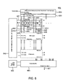
In an embodiment of the present invention, additional circuitry is included such that the memory may be configured as a content addressable memory (CAM). In one embodiment, the CAM uses 32 columns, and 64 word lines. One port of the memory is used, so the 64 word lines correspond to 64 rows of memory cells. The 64 rows are grouped into pairs or rows, with odd rows and neighboring even rows grouped together, specifically the first and second, the second and third, and so on. In a CAM, a data entry, for example a password, is stored. A data word, the comparand is entered. If there is a correspondence between the comparand and a data entry, a match is generated, otherwise there is a miss.
Specifically, in FIG. 8 , a data entry is stored in the odd memory cells in a column. A complement of the data entry is stored in the even memory cells in the column. Since in this example there are 32 columns, 32 data entries and their complements may be stored in this way. A comparand is then input to the word lines. In this CAM configuration, the usual word line decoder circuitry is bypassed, and comparand data inputs couple directly to the word lines. Specifically, the comparand data drives the even word lines, and a complement of the comparand data drives the odd word lines. In various embodiments of the present invention, the odd and even memory cells may be reversed, and the number of entries may be different.
The parallel impedance of the read cells in each column is then determined. If the impedance is high, there is a match, if the impedance is low, there is a miss. This means that for a match, each of the read cells in the column have a high impedance. This is because if only one impedance is low in a parallel combination, the impedance of the parallel combination is low. There are two devices in series in each read cell, an inverter device M5 730 and word line device M6 735. When a word line is selected, the word line device M6 735 is activated. That is, its gate is pulled high, and since in this example it is an N-channel or NMOS device, it may conduct. Whether an activated device actually conducts depends on the voltage at its source and drains relative to its gate and each other. Thus, for the impedance to be high in a selected read cell, the data stored at the memory cell node 753 is low, shutting off or deactivating M5 730. In this procedure, the data entry is stored in memory cells connected to word lines driven by the complement of the comparand, and the complement of the data entry is stored in word lines driven by the comparand. Thus, if there is a match between the data entry and the comparand, each selected word line drives a memory cell that is storing a low, and each memory cell that is storing a high, has an inactive word line. In this way, a match is detected by the high impedance of all the read cells in the column. Since each column has a sense amplifier, a simultaneous determination of whether there is a match is made between the comparand and each of the data entries.
Also, decoder circuitry is included in the sense amplifier block 860 in one embodiment of the present invention. Thus, if a sense amplifier reads a high impedance, the location of that sense amplifier is decoded, and output as a binary word. Specifically, a 5 bit binary word is output in this example, since there are 32 data entries, one per column, and 32 sense amplifiers. In various embodiments, the location of the lowest column, the highest column, or all the columns that have a match may be decoded.
In other embodiments, the CAM may have a different number of data entries, or not all data entries may be used. The size of the data entries may vary. The devices in the read cells may alternately be PMOS devices, bipolar devices, GAs or other such devices.
This memory may also be configured as a ROM, simply by not asserting the write enable signal. Also, it may be configured as a FIFO or LIFO (last-in-first-out). For these, a counter is made of surrounding programmable logic cells, and the counter controls the word line decoder. In a typical embodiment, the memory is an SRAM.
Again, in an embodiment of the present invention, the data input port is configurable to allow different sized data words. Since the number of bits in a data words is often smaller than the number of memory cells in a word line, the data words are multiplexed to various locations on a word line. FIGS. 13A , 13B, and 13C, illustrate the multiplexing and shifting of bits at the data input of a memory consistent with embodiments of the present invention. In one embodiment, these tasks are controlled by the write column select decoder. FIG. 13A is an example of a word line made up of 32 bits, accepting data from a 16-bit wide data input 1305. Data word 1305 may be written either to word line portion 1310 or 1315. To determine this, one extra bit of address is needed to select between the two word line portions. Similarly, multiplexing and shifting in the opposite direction occurs on a read.
This description of the invention has been presented for the purposes of illustration and description. It is not intended to be exhaustive or to limit the invention to the precise form described, and many modifications and variations are possible in light of the teaching above. The embodiments were chosen and described in order to best explain the principles of the invention and its practical applications. This description will enable others skilled in the art to best utilize and practice the invention in various embodiments and with various modifications as are suited to a particular use. This invention is defined by the following claims.
Claims (20)
1. A method of writing to a dual-port memory, the method comprising:
providing a data bit on a data line, and a complement of the data bit on a complementary data line;
selecting a word line to activate a first device coupled to the data line and a second device coupled to the complementary data line; and
selecting a column select line to activate a third device coupled between the first device and a first node of a memory cell, and a fourth device coupled between the second device and a second node of the memory cell.
2. The method of claim 1 further comprising:
before selecting the column select line, asserting a write enable.
3. The method of claim 2 further comprising:
deselecting the write enable; and
deactivating the third device and the fourth device.
4. The method of claim 3 wherein the first, second, third, and fourth devices are NMOS devices.
5. The method of claim 1 wherein the word line further couples to a read cell.
6. A method of determining the presence of a match between a data entry and a comparand in a content addressable memory, the content addressable memory comprising a plurality of memory storage cells arranged in rows and columns, each memory storage cell having a write circuit and a read circuit, wherein the write circuit and the read circuit of each memory storage cell in a row is coupled to one word line, and wherein the read cells of each memory storage cell in a column are coupled to one first read line and one second read line, the method comprising:
writing the data entry to odd numbered memory storage cells in a column of memory storage cells;
writing a complement of the data entry to even numbered memory storage cells in the column of memory storage cells;
driving word lines coupled to the even numbered memory storage cells in the column of memory storage cells with the comparand; and
driving word lines coupled to the odd numbered memory storage cells in the column of memory storage cells with a complement of the comparand.
7. The method of claim 5 further comprising:
determining a parallel impedance of the read cells in the column of memory storage cells, and outputting a match is the impedance is high.
8. The method of claim 6 further comprising decoding the position of the column of the match as a binary word.
9. The method of claim 7 wherein the data entries are product terms.
10. A method of writing to a dual-port memory comprising:
providing a data bit on a data line, and a complement of the data bit on a complementary data line;
asserting a write enable signal, which asserts a column select line thus activating a first and second device; and
asserting a word line thus activating a third and fourth device,
wherein the first and third devices are coupled between the data line and a first node of a memory cell, and the second and fourth devices are coupled between the complementary data line and a second node of the memory cell.
11. The method of claim 10 wherein a gate of the third device and a gate of the fourth device are coupled to the word line, and the third device is coupled to the data line and the fourth device is coupled to the complementary data line.
12. The method of claim 11 wherein the word line further couples to a read cell.
13. The method of claim 12 wherein a gate of the first device and a gate of the second device couple to the column select line.
14. The method of claim 13 wherein the first, second, third, and fourth devices are NMOS devices.
15. A method of reading data in a dual port memory comprising:
selecting a word line thus activating a first device; and
sensing an impedance between a first node and a second node,
wherein the first device and a second device are coupled in series between the first node and the second node, the second device having a gate coupled to a first node in a memory cell, and
wherein the word line couples to a third device and a fourth device, the third device and fourth devices used for writing to the memory cell.
16. The method of claim 15 wherein the third device couples between a data line and a fifth device and the fourth device couples between a complementary data line and a sixth device.
17. The method of claim 16 wherein the fifth device couples to the first node in the memory cell and the sixth device couples to a second node in the memory cell.
18. The method of claim 17 wherein a gate of the fifth device and a gate of the sixth device are coupled to a column select line, the column select line enabled by a write enable signal.
19. The method of claim 18 wherein the memory cell comprises a first inverter having an input and an output and a second inverter having an input and an output, the input of the first inverter coupled to the output of the second inverter, and the input of the second inverter coupled to the output of the first inverter.
20. The method of claim 15 wherein the first and second devices are NMOS devices.
Priority Applications (1)
| Application Number | Priority Date | Filing Date | Title |
|---|---|---|---|
| US10/696,209 US6992947B1 (en) | 2000-06-15 | 2003-10-28 | Dual-port SRAM in a programmable logic device |
Applications Claiming Priority (3)
| Application Number | Priority Date | Filing Date | Title |
|---|---|---|---|
| US21193600P | 2000-06-15 | 2000-06-15 | |
| US09/883,087 US6661733B1 (en) | 2000-06-15 | 2001-06-15 | Dual-port SRAM in a programmable logic device |
| US10/696,209 US6992947B1 (en) | 2000-06-15 | 2003-10-28 | Dual-port SRAM in a programmable logic device |
Related Parent Applications (1)
| Application Number | Title | Priority Date | Filing Date |
|---|---|---|---|
| US09/883,087 Division US6661733B1 (en) | 2000-06-15 | 2001-06-15 | Dual-port SRAM in a programmable logic device |
Publications (1)
| Publication Number | Publication Date |
|---|---|
| US6992947B1 true US6992947B1 (en) | 2006-01-31 |
Family
ID=29714810
Family Applications (3)
| Application Number | Title | Priority Date | Filing Date |
|---|---|---|---|
| US09/883,087 Expired - Lifetime US6661733B1 (en) | 2000-06-15 | 2001-06-15 | Dual-port SRAM in a programmable logic device |
| US10/046,939 Expired - Lifetime US6747903B1 (en) | 2000-06-15 | 2002-01-14 | Configurable decoder for addressing a memory |
| US10/696,209 Expired - Fee Related US6992947B1 (en) | 2000-06-15 | 2003-10-28 | Dual-port SRAM in a programmable logic device |
Family Applications Before (2)
| Application Number | Title | Priority Date | Filing Date |
|---|---|---|---|
| US09/883,087 Expired - Lifetime US6661733B1 (en) | 2000-06-15 | 2001-06-15 | Dual-port SRAM in a programmable logic device |
| US10/046,939 Expired - Lifetime US6747903B1 (en) | 2000-06-15 | 2002-01-14 | Configurable decoder for addressing a memory |
Country Status (1)
| Country | Link |
|---|---|
| US (3) | US6661733B1 (en) |
Cited By (8)
| Publication number | Priority date | Publication date | Assignee | Title |
|---|---|---|---|---|
| US7397726B1 (en) * | 2006-04-07 | 2008-07-08 | Altera Corporation | Flexible RAM clock enable |
| US20080212392A1 (en) * | 2007-03-02 | 2008-09-04 | Infineon Technologies | Multiple port mugfet sram |
| US20080244169A1 (en) * | 2007-03-30 | 2008-10-02 | Motorola, Inc. | Apparatus for Efficient Streaming Data Access on Reconfigurable Hardware and Method for Automatic Generation Thereof |
| US20090034356A1 (en) * | 2007-07-30 | 2009-02-05 | Donald Albert Evans | Dual-Port Memory |
| US20110134706A1 (en) * | 2006-02-08 | 2011-06-09 | Renesas Technology Corporation | Semiconductor memory device |
| US8190828B1 (en) | 2000-06-12 | 2012-05-29 | Altera Corporation | Embedded processor with dual-port SRAM for programmable logic |
| US20160372182A1 (en) * | 2013-03-11 | 2016-12-22 | Taiwan Semiconductor Manufacturing Co., Ltd. | Two-Port SRAM Connection Structure |
| CN109859791A (en) * | 2019-01-31 | 2019-06-07 | 西安微电子技术研究所 | A kind of 9 pipe SRAM memory cell of full isolation structure and its read-write operation method |
Families Citing this family (24)
| Publication number | Priority date | Publication date | Assignee | Title |
|---|---|---|---|---|
| US20020147934A1 (en) * | 2001-04-04 | 2002-10-10 | Anil Kavipurapu | Power selection system for use with a reconfigurable circuit and method of operating the same |
| US7184009B2 (en) * | 2002-06-21 | 2007-02-27 | Nokia Corporation | Display circuit with optical sensor |
| GB2393513A (en) * | 2002-09-25 | 2004-03-31 | Westerngeco Seismic Holdings | Marine seismic surveying using a source not having a ghost at a non-zero frequency |
| FR2850201A1 (en) * | 2003-01-21 | 2004-07-23 | St Microelectronics Sa | Address decoder for use with flash memory, has pilot of each word line including switching transistor to multiplex selection signal of groups and subgroups of word lines for applying one selected signal to word line |
| US6999372B2 (en) * | 2003-03-18 | 2006-02-14 | Sun Microsystems, Inc. | Multi-ported memory cell |
| GB2400662B (en) | 2003-04-15 | 2006-08-09 | Westerngeco Seismic Holdings | Active steering for marine seismic sources |
| US6982891B2 (en) * | 2003-06-10 | 2006-01-03 | Lsi Logic Corporation | Re-configurable content addressable/dual port memory |
| US7482657B1 (en) * | 2003-06-13 | 2009-01-27 | National Semiconductor Corporation | Balanced cells with fabrication mismatches that produce a unique number generator |
| JP2007529081A (en) * | 2003-07-01 | 2007-10-18 | ズィーモス テクノロジー,インコーポレイテッド | SRAM cell structure and circuit |
| US7353374B1 (en) * | 2004-06-22 | 2008-04-01 | Xilinx, Inc. | Integrated circuit with supervisory control circuit |
| US7320064B2 (en) * | 2004-07-23 | 2008-01-15 | Honeywell International Inc. | Reconfigurable computing architecture for space applications |
| US7110304B1 (en) | 2004-08-26 | 2006-09-19 | Altera Corporation | Dual port memory array using shared write drivers and read sense amplifiers |
| US7307912B1 (en) | 2004-10-25 | 2007-12-11 | Lattice Semiconductor Corporation | Variable data width memory systems and methods |
| US7130238B1 (en) | 2005-01-21 | 2006-10-31 | Altera Corporation | Divisible true dual port memory system supporting simple dual port memory subsystems |
| JP2006209877A (en) * | 2005-01-28 | 2006-08-10 | Nec Electronics Corp | Semiconductor storage device |
| US7304352B2 (en) * | 2005-04-21 | 2007-12-04 | International Business Machines Corporation | Alignment insensitive D-cache cell |
| US20070046781A1 (en) * | 2005-08-29 | 2007-03-01 | Honeywell International Inc. | Systems and methods for processing digital video data |
| US7196963B1 (en) * | 2005-10-17 | 2007-03-27 | Lattice Semiconductor Corporation | Address isolation for user-defined configuration memory in programmable devices |
| US7898894B2 (en) * | 2006-04-12 | 2011-03-01 | International Business Machines Corporation | Static random access memory (SRAM) cells |
| US20080022081A1 (en) * | 2006-07-18 | 2008-01-24 | Honeywell International Inc. | Local controller for reconfigurable processing elements |
| US20080024165A1 (en) * | 2006-07-28 | 2008-01-31 | Raminda Udaya Madurawe | Configurable embedded multi-port memory |
| US9208109B2 (en) * | 2011-06-01 | 2015-12-08 | Altera Corporation | Memory controllers with dynamic port priority assignment capabilities |
| US10008257B2 (en) * | 2015-11-20 | 2018-06-26 | Oracle International Corporation | Memory bitcell with column select |
| US10553275B2 (en) * | 2017-04-18 | 2020-02-04 | Taiwan Semiconductor Manufacturing Company, Ltd. | Device having write assist circuit including memory-adapted transistors and method for making the same |
Citations (3)
| Publication number | Priority date | Publication date | Assignee | Title |
|---|---|---|---|---|
| US5307322A (en) * | 1991-07-03 | 1994-04-26 | Kabushiki Kaisha Toshiba | Memory cell for use in a multi-port RAM |
| US6044034A (en) * | 1998-03-16 | 2000-03-28 | Fujitsu Limited | Multiport memory having plurality of groups of bit lines |
| US6400635B1 (en) * | 2000-03-15 | 2002-06-04 | Altera Corporation | Memory circuitry for programmable logic integrated circuit devices |
Family Cites Families (3)
| Publication number | Priority date | Publication date | Assignee | Title |
|---|---|---|---|---|
| US6020759A (en) * | 1997-03-21 | 2000-02-01 | Altera Corporation | Programmable logic array device with random access memory configurable as product terms |
| US6262933B1 (en) * | 1999-01-29 | 2001-07-17 | Altera Corporation | High speed programmable address decoder |
| US6396302B2 (en) * | 1999-02-25 | 2002-05-28 | Xilinx, Inc. | Configurable logic element with expander structures |
-
2001
- 2001-06-15 US US09/883,087 patent/US6661733B1/en not_active Expired - Lifetime
-
2002
- 2002-01-14 US US10/046,939 patent/US6747903B1/en not_active Expired - Lifetime
-
2003
- 2003-10-28 US US10/696,209 patent/US6992947B1/en not_active Expired - Fee Related
Patent Citations (3)
| Publication number | Priority date | Publication date | Assignee | Title |
|---|---|---|---|---|
| US5307322A (en) * | 1991-07-03 | 1994-04-26 | Kabushiki Kaisha Toshiba | Memory cell for use in a multi-port RAM |
| US6044034A (en) * | 1998-03-16 | 2000-03-28 | Fujitsu Limited | Multiport memory having plurality of groups of bit lines |
| US6400635B1 (en) * | 2000-03-15 | 2002-06-04 | Altera Corporation | Memory circuitry for programmable logic integrated circuit devices |
Cited By (13)
| Publication number | Priority date | Publication date | Assignee | Title |
|---|---|---|---|---|
| US8190828B1 (en) | 2000-06-12 | 2012-05-29 | Altera Corporation | Embedded processor with dual-port SRAM for programmable logic |
| US20110134706A1 (en) * | 2006-02-08 | 2011-06-09 | Renesas Technology Corporation | Semiconductor memory device |
| US8238192B2 (en) | 2006-02-08 | 2012-08-07 | Renesas Electronics Corporation | Semiconductor memory device having multiple ports |
| US7397726B1 (en) * | 2006-04-07 | 2008-07-08 | Altera Corporation | Flexible RAM clock enable |
| US20080212392A1 (en) * | 2007-03-02 | 2008-09-04 | Infineon Technologies | Multiple port mugfet sram |
| US7483283B2 (en) * | 2007-03-30 | 2009-01-27 | Motorola, Inc. | Apparatus for efficient streaming data access on reconfigurable hardware and method for automatic generation thereof |
| US20080244169A1 (en) * | 2007-03-30 | 2008-10-02 | Motorola, Inc. | Apparatus for Efficient Streaming Data Access on Reconfigurable Hardware and Method for Automatic Generation Thereof |
| US7551512B2 (en) * | 2007-07-30 | 2009-06-23 | Agere Systems Inc. | Dual-port memory |
| US20090034356A1 (en) * | 2007-07-30 | 2009-02-05 | Donald Albert Evans | Dual-Port Memory |
| US20160372182A1 (en) * | 2013-03-11 | 2016-12-22 | Taiwan Semiconductor Manufacturing Co., Ltd. | Two-Port SRAM Connection Structure |
| US9672903B2 (en) * | 2013-03-11 | 2017-06-06 | Taiwan Semicondutor Manufacturing Co., Ltd. | Two-port SRAM connection structure |
| US10163495B2 (en) | 2013-03-11 | 2018-12-25 | Taiwan Semiconductor Manufacturing Company, Ltd. | Two-port SRAM connection structure |
| CN109859791A (en) * | 2019-01-31 | 2019-06-07 | 西安微电子技术研究所 | A kind of 9 pipe SRAM memory cell of full isolation structure and its read-write operation method |
Also Published As
| Publication number | Publication date |
|---|---|
| US6747903B1 (en) | 2004-06-08 |
| US6661733B1 (en) | 2003-12-09 |
Similar Documents
| Publication | Publication Date | Title |
|---|---|---|
| US6992947B1 (en) | Dual-port SRAM in a programmable logic device | |
| US6038627A (en) | SRAM bus architecture and interconnect to an FPGA | |
| US6430088B1 (en) | Embedded static random access memory for field programmable gate array | |
| US6915323B1 (en) | Macrocells supporting a carry cascade | |
| US6347061B1 (en) | Programmable logic array device with random access memory configurable as product terms | |
| EP0925649B1 (en) | Fpga architecture having ram blocks with programmable word length and width and dedicated address and data lines | |
| US6184707B1 (en) | Look-up table based logic element with complete permutability of the inputs to the secondary signals | |
| EP0840455B1 (en) | A microcontroller accessible macrocell | |
| US7289372B1 (en) | Dual-port memory array using shared write drivers and read sense amplifiers | |
| US6803785B1 (en) | I/O circuitry shared between processor and programmable logic portions of an integrated circuit | |
| US7088134B1 (en) | Programmable logic device with flexible memory allocation and routing | |
| US10020811B2 (en) | FPGA RAM blocks optimized for use as register files | |
| US6346825B1 (en) | Block RAM with configurable data width and parity for use in a field programmable gate array | |
| US7269089B1 (en) | Divisible true dual port memory system supporting simple dual port memory subsystems | |
| US7444456B2 (en) | SRAM bus architecture and interconnect to an FPGA | |
| US7304499B1 (en) | Distributed random access memory in a programmable logic device | |
| US6486702B1 (en) | Embedded memory blocks for programmable logic | |
| US6262933B1 (en) | High speed programmable address decoder | |
| US7248491B1 (en) | Circuit for and method of implementing a content addressable memory in a programmable logic device | |
| US6011740A (en) | Structure and method for providing additional configuration memories on an FPGA | |
| KR100240913B1 (en) | Methods and systems for improving memory component size and access speed, including splitting bit lines and alternate pre-charge/access cycles | |
| US7242633B1 (en) | Memory device and method of transferring data in memory device | |
| US7639557B1 (en) | Configurable random-access-memory circuitry | |
| US6356110B1 (en) | Multifunction memory array in a programmable logic device | |
| US7071731B1 (en) | Programmable Logic with Pipelined Memory Operation |
Legal Events
| Date | Code | Title | Description |
|---|---|---|---|
| FPAY | Fee payment |
Year of fee payment: 4 |
|
| FPAY | Fee payment |
Year of fee payment: 8 |
|
| FEPP | Fee payment procedure |
Free format text: MAINTENANCE FEE REMINDER MAILED (ORIGINAL EVENT CODE: REM.) |
|
| LAPS | Lapse for failure to pay maintenance fees |
Free format text: PATENT EXPIRED FOR FAILURE TO PAY MAINTENANCE FEES (ORIGINAL EVENT CODE: EXP.) |
|
| STCH | Information on status: patent discontinuation |
Free format text: PATENT EXPIRED DUE TO NONPAYMENT OF MAINTENANCE FEES UNDER 37 CFR 1.362 |
|
| FP | Expired due to failure to pay maintenance fee |
Effective date: 20180131 |