US7008872B2 - Use of conductive electrolessly deposited etch stop layers, liner layers and via plugs in interconnect structures - Google Patents
Use of conductive electrolessly deposited etch stop layers, liner layers and via plugs in interconnect structures Download PDFInfo
- Publication number
- US7008872B2 US7008872B2 US10/139,052 US13905202A US7008872B2 US 7008872 B2 US7008872 B2 US 7008872B2 US 13905202 A US13905202 A US 13905202A US 7008872 B2 US7008872 B2 US 7008872B2
- Authority
- US
- United States
- Prior art keywords
- layer
- conductive material
- electrolessly
- interconnect line
- interconnect
- Prior art date
- Legal status (The legal status is an assumption and is not a legal conclusion. Google has not performed a legal analysis and makes no representation as to the accuracy of the status listed.)
- Expired - Lifetime
Links
Images


Classifications
-
- H—ELECTRICITY
- H01—ELECTRIC ELEMENTS
- H01L—SEMICONDUCTOR DEVICES NOT COVERED BY CLASS H10
- H01L21/00—Processes or apparatus adapted for the manufacture or treatment of semiconductor or solid state devices or of parts thereof
- H01L21/70—Manufacture or treatment of devices consisting of a plurality of solid state components formed in or on a common substrate or of parts thereof; Manufacture of integrated circuit devices or of parts thereof
- H01L21/71—Manufacture of specific parts of devices defined in group H01L21/70
- H01L21/768—Applying interconnections to be used for carrying current between separate components within a device comprising conductors and dielectrics
- H01L21/76838—Applying interconnections to be used for carrying current between separate components within a device comprising conductors and dielectrics characterised by the formation and the after-treatment of the conductors
- H01L21/76841—Barrier, adhesion or liner layers
- H01L21/76843—Barrier, adhesion or liner layers formed in openings in a dielectric
-
- H—ELECTRICITY
- H01—ELECTRIC ELEMENTS
- H01L—SEMICONDUCTOR DEVICES NOT COVERED BY CLASS H10
- H01L21/00—Processes or apparatus adapted for the manufacture or treatment of semiconductor or solid state devices or of parts thereof
- H01L21/02—Manufacture or treatment of semiconductor devices or of parts thereof
- H01L21/04—Manufacture or treatment of semiconductor devices or of parts thereof the devices having at least one potential-jump barrier or surface barrier, e.g. PN junction, depletion layer or carrier concentration layer
- H01L21/18—Manufacture or treatment of semiconductor devices or of parts thereof the devices having at least one potential-jump barrier or surface barrier, e.g. PN junction, depletion layer or carrier concentration layer the devices having semiconductor bodies comprising elements of Group IV of the Periodic System or AIIIBV compounds with or without impurities, e.g. doping materials
- H01L21/28—Manufacture of electrodes on semiconductor bodies using processes or apparatus not provided for in groups H01L21/20 - H01L21/268
- H01L21/283—Deposition of conductive or insulating materials for electrodes conducting electric current
- H01L21/288—Deposition of conductive or insulating materials for electrodes conducting electric current from a liquid, e.g. electrolytic deposition
-
- H—ELECTRICITY
- H01—ELECTRIC ELEMENTS
- H01L—SEMICONDUCTOR DEVICES NOT COVERED BY CLASS H10
- H01L21/00—Processes or apparatus adapted for the manufacture or treatment of semiconductor or solid state devices or of parts thereof
- H01L21/70—Manufacture or treatment of devices consisting of a plurality of solid state components formed in or on a common substrate or of parts thereof; Manufacture of integrated circuit devices or of parts thereof
- H01L21/71—Manufacture of specific parts of devices defined in group H01L21/70
- H01L21/768—Applying interconnections to be used for carrying current between separate components within a device comprising conductors and dielectrics
- H01L21/76838—Applying interconnections to be used for carrying current between separate components within a device comprising conductors and dielectrics characterised by the formation and the after-treatment of the conductors
- H01L21/76841—Barrier, adhesion or liner layers
- H01L21/76843—Barrier, adhesion or liner layers formed in openings in a dielectric
- H01L21/76849—Barrier, adhesion or liner layers formed in openings in a dielectric the layer being positioned on top of the main fill metal
-
- H—ELECTRICITY
- H01—ELECTRIC ELEMENTS
- H01L—SEMICONDUCTOR DEVICES NOT COVERED BY CLASS H10
- H01L21/00—Processes or apparatus adapted for the manufacture or treatment of semiconductor or solid state devices or of parts thereof
- H01L21/70—Manufacture or treatment of devices consisting of a plurality of solid state components formed in or on a common substrate or of parts thereof; Manufacture of integrated circuit devices or of parts thereof
- H01L21/71—Manufacture of specific parts of devices defined in group H01L21/70
- H01L21/768—Applying interconnections to be used for carrying current between separate components within a device comprising conductors and dielectrics
- H01L21/76838—Applying interconnections to be used for carrying current between separate components within a device comprising conductors and dielectrics characterised by the formation and the after-treatment of the conductors
- H01L21/76841—Barrier, adhesion or liner layers
- H01L21/7685—Barrier, adhesion or liner layers the layer covering a conductive structure
- H01L21/76852—Barrier, adhesion or liner layers the layer covering a conductive structure the layer also covering the sidewalls of the conductive structure
-
- H—ELECTRICITY
- H01—ELECTRIC ELEMENTS
- H01L—SEMICONDUCTOR DEVICES NOT COVERED BY CLASS H10
- H01L21/00—Processes or apparatus adapted for the manufacture or treatment of semiconductor or solid state devices or of parts thereof
- H01L21/70—Manufacture or treatment of devices consisting of a plurality of solid state components formed in or on a common substrate or of parts thereof; Manufacture of integrated circuit devices or of parts thereof
- H01L21/71—Manufacture of specific parts of devices defined in group H01L21/70
- H01L21/768—Applying interconnections to be used for carrying current between separate components within a device comprising conductors and dielectrics
- H01L21/76838—Applying interconnections to be used for carrying current between separate components within a device comprising conductors and dielectrics characterised by the formation and the after-treatment of the conductors
- H01L21/76841—Barrier, adhesion or liner layers
- H01L21/76853—Barrier, adhesion or liner layers characterized by particular after-treatment steps
- H01L21/76861—Post-treatment or after-treatment not introducing additional chemical elements into the layer
- H01L21/76864—Thermal treatment
-
- H—ELECTRICITY
- H01—ELECTRIC ELEMENTS
- H01L—SEMICONDUCTOR DEVICES NOT COVERED BY CLASS H10
- H01L21/00—Processes or apparatus adapted for the manufacture or treatment of semiconductor or solid state devices or of parts thereof
- H01L21/70—Manufacture or treatment of devices consisting of a plurality of solid state components formed in or on a common substrate or of parts thereof; Manufacture of integrated circuit devices or of parts thereof
- H01L21/71—Manufacture of specific parts of devices defined in group H01L21/70
- H01L21/768—Applying interconnections to be used for carrying current between separate components within a device comprising conductors and dielectrics
- H01L21/76838—Applying interconnections to be used for carrying current between separate components within a device comprising conductors and dielectrics characterised by the formation and the after-treatment of the conductors
- H01L21/76841—Barrier, adhesion or liner layers
- H01L21/76868—Forming or treating discontinuous thin films, e.g. repair, enhancement or reinforcement of discontinuous thin films
-
- H—ELECTRICITY
- H01—ELECTRIC ELEMENTS
- H01L—SEMICONDUCTOR DEVICES NOT COVERED BY CLASS H10
- H01L21/00—Processes or apparatus adapted for the manufacture or treatment of semiconductor or solid state devices or of parts thereof
- H01L21/70—Manufacture or treatment of devices consisting of a plurality of solid state components formed in or on a common substrate or of parts thereof; Manufacture of integrated circuit devices or of parts thereof
- H01L21/71—Manufacture of specific parts of devices defined in group H01L21/70
- H01L21/768—Applying interconnections to be used for carrying current between separate components within a device comprising conductors and dielectrics
- H01L21/76838—Applying interconnections to be used for carrying current between separate components within a device comprising conductors and dielectrics characterised by the formation and the after-treatment of the conductors
- H01L21/76841—Barrier, adhesion or liner layers
- H01L21/76871—Layers specifically deposited to enhance or enable the nucleation of further layers, i.e. seed layers
- H01L21/76874—Layers specifically deposited to enhance or enable the nucleation of further layers, i.e. seed layers for electroless plating
-
- H—ELECTRICITY
- H01—ELECTRIC ELEMENTS
- H01L—SEMICONDUCTOR DEVICES NOT COVERED BY CLASS H10
- H01L21/00—Processes or apparatus adapted for the manufacture or treatment of semiconductor or solid state devices or of parts thereof
- H01L21/70—Manufacture or treatment of devices consisting of a plurality of solid state components formed in or on a common substrate or of parts thereof; Manufacture of integrated circuit devices or of parts thereof
- H01L21/71—Manufacture of specific parts of devices defined in group H01L21/70
- H01L21/768—Applying interconnections to be used for carrying current between separate components within a device comprising conductors and dielectrics
- H01L21/76838—Applying interconnections to be used for carrying current between separate components within a device comprising conductors and dielectrics characterised by the formation and the after-treatment of the conductors
- H01L21/76877—Filling of holes, grooves or trenches, e.g. vias, with conductive material
- H01L21/76879—Filling of holes, grooves or trenches, e.g. vias, with conductive material by selective deposition of conductive material in the vias, e.g. selective C.V.D. on semiconductor material, plating
-
- H—ELECTRICITY
- H01—ELECTRIC ELEMENTS
- H01L—SEMICONDUCTOR DEVICES NOT COVERED BY CLASS H10
- H01L23/00—Details of semiconductor or other solid state devices
- H01L23/52—Arrangements for conducting electric current within the device in operation from one component to another, i.e. interconnections, e.g. wires, lead frames
- H01L23/522—Arrangements for conducting electric current within the device in operation from one component to another, i.e. interconnections, e.g. wires, lead frames including external interconnections consisting of a multilayer structure of conductive and insulating layers inseparably formed on the semiconductor body
- H01L23/532—Arrangements for conducting electric current within the device in operation from one component to another, i.e. interconnections, e.g. wires, lead frames including external interconnections consisting of a multilayer structure of conductive and insulating layers inseparably formed on the semiconductor body characterised by the materials
- H01L23/53204—Conductive materials
- H01L23/53209—Conductive materials based on metals, e.g. alloys, metal silicides
- H01L23/53228—Conductive materials based on metals, e.g. alloys, metal silicides the principal metal being copper
- H01L23/53238—Additional layers associated with copper layers, e.g. adhesion, barrier, cladding layers
-
- H—ELECTRICITY
- H01—ELECTRIC ELEMENTS
- H01L—SEMICONDUCTOR DEVICES NOT COVERED BY CLASS H10
- H01L21/00—Processes or apparatus adapted for the manufacture or treatment of semiconductor or solid state devices or of parts thereof
- H01L21/70—Manufacture or treatment of devices consisting of a plurality of solid state components formed in or on a common substrate or of parts thereof; Manufacture of integrated circuit devices or of parts thereof
- H01L21/71—Manufacture of specific parts of devices defined in group H01L21/70
- H01L21/768—Applying interconnections to be used for carrying current between separate components within a device comprising conductors and dielectrics
- H01L21/76801—Applying interconnections to be used for carrying current between separate components within a device comprising conductors and dielectrics characterised by the formation and the after-treatment of the dielectrics, e.g. smoothing
- H01L21/76802—Applying interconnections to be used for carrying current between separate components within a device comprising conductors and dielectrics characterised by the formation and the after-treatment of the dielectrics, e.g. smoothing by forming openings in dielectrics
- H01L21/76807—Applying interconnections to be used for carrying current between separate components within a device comprising conductors and dielectrics characterised by the formation and the after-treatment of the dielectrics, e.g. smoothing by forming openings in dielectrics for dual damascene structures
-
- H—ELECTRICITY
- H01—ELECTRIC ELEMENTS
- H01L—SEMICONDUCTOR DEVICES NOT COVERED BY CLASS H10
- H01L2924/00—Indexing scheme for arrangements or methods for connecting or disconnecting semiconductor or solid-state bodies as covered by H01L24/00
- H01L2924/0001—Technical content checked by a classifier
- H01L2924/0002—Not covered by any one of groups H01L24/00, H01L24/00 and H01L2224/00
-
- H—ELECTRICITY
- H01—ELECTRIC ELEMENTS
- H01L—SEMICONDUCTOR DEVICES NOT COVERED BY CLASS H10
- H01L2924/00—Indexing scheme for arrangements or methods for connecting or disconnecting semiconductor or solid-state bodies as covered by H01L24/00
- H01L2924/30—Technical effects
- H01L2924/301—Electrical effects
- H01L2924/3011—Impedance
Definitions
- Embodiments of the present invention relate to interconnect structures and fabrication methods.
- the embodiments relate to novel interconnect structures containing conductive electrolessly deposited etch stop layers and in some instances liner layers and via plugs, to novel methods for making the interconnect structures, and to integrated circuits containing the interconnect structures.
- interconnect structures to provide electrical signals to logic elements such as transistors located on a semiconductor substrate.
- the interconnect structures often contain interconnect lines which are spaced apart in a nearly coplanar arrangement within a dielectric material that insulates the lines from one another. Select connections between interconnect lines on different levels are made by vias formed through the insulating material.
- the interconnect lines are often made of highly conductive metals or alloys. Copper has become a widely used material due in part to its low electrical resistance compared to other metals. However, one of the disadvantages of copper is that it readily oxidizes. Accordingly, if a copper surface is left exposed for prolonged periods of time, or subjected to a variety of etching or plasma cleaning operations, the surface may become oxidized. Unlike with other materials, such as aluminum, copper oxidation does not lead to a thin protective coating that blocks further oxidation, and significant portions of the copper may become oxidized. This is generally undesirable, since it may significant change the electrical and mechanical properties of the interconnect structure. Another disadvantage of copper is that it is easily etched with many of the commonly used dielectric etching chemistries. Accordingly, if the copper surface is left exposed, and unprotected, it can become oxidized or partly removed during subsequent processing operations.
- protective dielectric etch stop or hard mask layers are often formed on copper interconnect lines.
- Materials that are commonly used for this purpose include silicon nitride (SiN), silicon carbide (SiC), and silicon dioxide (SiO 2 ).
- SiN silicon nitride
- SiC silicon carbide
- SiO 2 silicon dioxide
- the protective dielectric layers provide an additional material interface or junction where mechanical separation from the protective layers in the form of pilling, cracking, or blistering often occurs. These types of mechanical failures may reduce production yields and may decrease the effective lifetime of manufactured integrated circuits. This problem may be compounded when low dielectric constant materials (low-k), which have a dielectric constant less than silicon dioxide, are used for the interconnect structure, since these materials are often chemically different from the protective dielectric layer materials.
- low dielectric constant materials low-k
- the protective dielectric materials may also increase the effective dielectric constant of the interconnect structure, particularly when the structure contains low-k dielectric materials. Such increases in the dielectric constant may effectively decrease the speed of the integrated circuit, which depends upon interconnect signal propagation speeds. This can lead to reduced performance of the integrated circuit.
- FIG. 1 shows a cross-sectional view of an integrated circuit substrate containing a semiconductor substrate, a dielectric layer formed on the substrate, and a trench formed within the dielectric layer to accommodate an interconnect line, according to one embodiment of the present invention.
- FIG. 2 shows a cross-sectional view of an integrated circuit substrate after forming a liner layer and seed material on the dielectric layer and within the trench of FIG. 1 , according to one embodiment of the present invention.
- FIG. 3 shows a cross-sectional view of an integrated circuit substrate after forming a conductive layer (typically a metal layer) on the seed layer and within the trench of FIG. 2 , according to one embodiment of the present invention.
- a conductive layer typically a metal layer
- FIG. 4 shows a cross-sectional view of an integrated circuit substrate after removing portions of the conductive layer, liner, and seed material outside the trench from the substrate of FIG. 3 , according to one embodiment of the present invention.
- FIG. 5 shows a cross-sectional view of an integrated circuit substrate after forming a conductive electrolessly deposited layer over the interconnect line of FIG. 4 , according to one embodiment of the present invention.
- FIG. 6 shows a cross-sectional view of an integrated circuit substrate after forming a second dielectric layer on the existing dielectric layer and the conductive electroless layer of FIG. 5 , according to one embodiment of the present invention.
- FIG. 7 shows a cross-sectional view of an integrated circuit substrate after forming an opening to accommodate a via in the second dielectric layer of FIG. 6 , according to one embodiment of the present invention.
- FIG. 8 shows a cross-sectional view of an integrated circuit substrate after forming an opening to accommodate a second interconnect line at the top of the via opening of FIG. 7 , according to one embodiment of the present invention.
- FIG. 9 shows a cross-sectional view of an integrated circuit substrate after adding conductive interconnect material to fill the opening of FIG. 8 , according to one embodiment of the present invention.
- FIG. 10 shows a cross-sectional view of an integrated circuit substrate after forming a conductive electrolessly deposited layer on top of the conductive interconnect material (the second interconnect line) of FIG. 9 , according to one embodiment of the present invention.
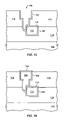
- FIG. 11 shows a cross-sectional view of an integrated circuit substrate after forming an opening to accommodate an unlanded via in dielectric layers such as those shown in FIG. 6 , according to one embodiment of the present invention.
- FIG. 12 shows a cross-sectional view of an integrated circuit substrate containing a multi-level interconnect structure having an electrolessly deposited conductive layer as an etch stop layer for an unlanded via, according to one embodiment of the present invention.
- FIG. 13 shows a cross-sectional view of an integrated circuit substrate after forming an unlanded via by electrolessly depositing a conductive material on a bottom portion of an opening, according to one embodiment of the present invention.
- FIG. 14 shows a cross-sectional view of an integrated circuit substrate containing a multi-level interconnect structure having a conductive electrolessly deposited via plug, according to one embodiment of the present invention.
- FIG. 15 shows a cross-sectional view of an integrated circuit substrate after forming a liner layer on exposed surfaces of an opening, according to one embodiment of the present invention.
- FIG. 16 shows a cross-sectional view of an integrated circuit substrate containing a multi-level interconnect structure having an electrolessly deposited liner layer as a barrier between interconnect materials and dielectric, according to one embodiment of the present invention.
- FIG. 17 shows a cross-sectional view of an integrated circuit substrate after forming a recessed interconnect line by removing material from a top exposed surface of an interconnect line such as the one shown in FIG. 4 , according to one embodiment of the present invention.
- FIG. 18 shows a cross-sectional view of an integrated circuit substrate after forming an inlaid conductive electrolessly deposited layer over the recessed interconnect line of FIG. 17 , according to one embodiment of the present invention.
- FIG. 19 shows a computer system containing a microprocessor having an interconnect structure, in accordance with an embodiment of the present invention.
- interconnect structures containing conductive electrolessly deposited etch stop layers, and in some embodiments liner layers or via plugs, and methods for fabricating the interconnect structures.
- numerous specific details are set forth. However, it is understood that embodiments of the invention may be practiced without these specific details. For example, well-known equivalent materials may be substituted in place of those described herein, and similarly, well-known equivalent techniques may be substituted in place of the particular processing techniques disclosed. In other instances, well-known circuits, structures and techniques have not been shown in detail to avoid obscuring the understanding of this description.
- FIGS. 1–10 show cross-sectional views of substrates representing different stages of a method for fabricating an interconnect structure containing a conductive layer formed over an interconnect line in accordance with one embodiment of the present invention.
- the conductive layer serves as both an etch stop landing for a via formed over the interconnect line and as a shunt for flow of current between the interconnect line and the via.
- FIG. 1 shows a cross-sectional view of a portion of an integrated circuit substrate containing a semiconductor substrate 102 having circuit components formed therein, a first dielectric layer 104 formed on the substrate, and a trench opening 106 formed within the dielectric layer.
- the dielectric layer may be formed on the substrate using deposition techniques that are well-known in the semiconductor processing arts.
- a low-k dielectric material such as a fluorinated oxide of silicon (e.g., SiOF) or carbon doped oxide of silicon (e.g., carbon doped silicon dioxide, SiO 2 ) may be deposited by Chemical Vapor Deposition (CVD).
- the trench 106 may be formed within the dielectric layer by using well-known masking, lithography, and etching techniques.
- a radiation sensitive layer e.g., a positive or negative photoresist
- a portion of the radiation sensitive layer superjacent the trench may be removed, a corresponding portion of the dielectric layer removed by etching, and then the remainder of the of the radiation sensitive layer may be removed.
- FIG. 2 shows a cross-sectional view of a portion of an integrated circuit substrate after forming a liner layer 108 and seed material 110 on dielectric layer 104 of FIG. 1 .
- the liner layer may be used to prevent undesirable interactions between material to be subsequently deposited in the trench and the dielectric material of the layer 104 .
- the liner may be formed by depositing a thin layer of a suitable material over the surface of the dielectric layer, including on the inner surfaces of the trench 106 .
- the liner often has a thickness between about 10–50 Angstroms (an Angstrom is 1/10,000,000,000 of a meter, or one-tenth of a nanometer).
- Suitable materials for the liner include barrier layer refractory metals and alloys, such as molybdenum, nickel, cobalt, cobalt-nickel (CoNi), titanium-tungston (TiW), tantalum (Ta), tantalum-nitride (TaN), tantalum-silicon-nitride (TaSiN), titanium-nitride (TiN), titanium-silicon-nitride (TiSiN), tungsten (W), tungsten-nitride (WN), tungsten-silicon-nitride (WiSiN), and combinations of such materials (e.g., a multi-layer stack of Ta/TaN).
- Suitable well-known deposition techniques such as CVD, Atomic Layer Deposition (ALD), or Physical Vapor Deposition (PVD) may be used to deposit these various materials.
- a small amount of the seed material 110 may be formed over the liner by a deposition process such as PVD or CVD in order to improve the subsequent deposition of conductive interconnect materials. As shown, less than a monolayer of seed material may be used for a subsequent electroless deposition. Of course, a monolayer or more may also be used. Often, if the seed material is used for an electroplating deposition at least a monolayer and often a thickness between about 30–3000 Angstroms will be used.
- the seed material contains copper (Cu) or an alloy of copper (e.g., copper-tin (CuSn), copper-indium (CuIn), copper-magnesium (CuMg), copper-aluminum (CuAl)) to assist with a subsequent formation of a copper containing material thereon.
- Cu copper
- an alloy of copper e.g., copper-tin (CuSn), copper-indium (CuIn), copper-magnesium (CuMg), copper-aluminum (CuAl)
- Cu copper-tin
- CuIn copper-indium
- CuMg copper-magnesium
- CuAl copper-aluminum
- FIG. 3 shows a cross-sectional view of a portion of an integrated circuit substrate after forming a conductive layer 112 on the seed layer 110 of FIG. 2 .
- the conductive layer often contains a metal or alloy.
- the term metal will be used to include pure metals, mixtures or alloys of multiple metals, and mixtures or alloys of a metal and one or more non-metals (e.g., metalloids or non-metals).
- the layer contains a conductive copper material.
- Exemplary copper materials include but are not limited to pure copper, or an alloy such as copper-tin (CuSn), copper-indium (CuIn), copper-antimony (GuSb), copper-bismuth (CuBi), copper-rhenium (CuRe).
- the material may be deposited by an electroless, electroplating or other process.
- An electroless deposition process differs from an electroplating process in that there is no externally supplied current from a voltage source. Although electroplating processes are commonly used, an electroless deposition may be favored for a deep, narrow, high aspect ratio trench, since continuous and thick seed layers are not needed for electroless deposition. Both depositions are well-known in the semiconductor processing arts.
- FIG. 4 shows a cross-sectional view of a portion of an integrated circuit substrate after removing portions of the conductive layer 112 , liner 108 , and seed material (not shown), that lie outside the trench, from the substrate of FIG. 3 .
- These portions are typically removed by planarizing the upper surface with a chemical-mechanical polishing (CMP) or mechanical polishing, although this is not required.
- CMP chemical-mechanical polishing
- Those skilled in the art and having the benefit of this disclosure will recognize that depending on the thickness of the layer and the degree of planarity with which they are formed, it may be possible to eliminate this particular planarization operation. Removal of these portions creates a patterned interconnect line 112 containing conductive material within the trench.
- the interconnect line represents any patterned conductive material suitable to provide a signaling medium to carry electrical signals.
- interconnect lines are sometimes referred to as traces, wires, lines, interconnect or simply metal.
- FIG. 5 shows a cross-sectional view of a portion of an integrated circuit substrate after forming a conductive layer 114 containing an electrolessly deposited metal over the interconnect line 112 of FIG. 4 .
- a conductive layer 114 containing an electrolessly deposited metal over the interconnect line 112 of FIG. 4 .
- cleaning is not required, it may nevertheless assist in forming quality, homogeneous conductive layers.
- a variety of cleansers may be adapted for cleaning the substrate of FIG. 4 .
- One particular cleanser that has been found to be useful for removing organic impurities that can be formed on the surface during CMP includes a hot deionized water solution containing effective amounts of a surfactant to help wet the surface, an etching agent sufficient to slowly etch a copper interconnect line to assist with removing organic that is tightly bonded to the copper, and a reducing agent to reduce the oxidation number of the copper and help activate it for the subsequent electroless deposition.
- Suitable surfactants include but are not limited to RHODAFAC #RE610, available from Rhone-Poulenc, and Triton X100, available from Sigma-Aldrich.
- Suitable etching agents include an appropriately weak solution of an acid with ⁇ 10 wt % in water (e.g., a strong mineral acid like hydrofluoric acid, nitric acid, or sulfuric acid, or a weak organic or carboxylic acid like citric acid or malonic acid). Ammonia may also be used to etch a copper material. Suitable reducing agents include among others glyoxylic acid.
- the cleanser may contain other agents such as a base like TMAH (tetra methyl ammonium hydroxide) or potassium hydroxide and an oxidizer like hydrogen peroxide.
- TMAH tetra methyl ammonium hydroxide
- the base is often used in an aqueous concentration of less then about 10 wt %.
- these cleaners may be replaced by other cleaners, or cleaning avoided altogether, so long as the surface of the interconnect line is sufficiently clean to allow electroless deposition of the cobalt alloy layer. Sonic agitation or scrubbing may be used in order to dislodge particles and improve cleaning.
- the conductive electrolessly deposited layer 114 has been formed on the exposed (often cleaned) surface of the interconnect line 112 of FIG. 4 .
- the layer often forms on the liner layer 108 although this depends upon the particular materials.
- the layer may have a range of thickness, including a thickness between about 10–100 nanometers in one instance.
- the layer 114 may passivate and protect the interconnect line 112 and may serve as an etch stop layer during fabrication and as a conductive shunt layer during device operation.
- the layer 114 may be formed by chemical deposition of a metal through a chemical reaction.
- the layer may be formed by an electroless deposition wherein a substrate is placed in a solution, containing a metal containing compound (e.g., a metal complex) and a reducing agent, and a metal is deposited at an electrochemically active surface of the substrate through an autocatalytic oxidation-reduction (redox) reaction between the metal containing compound and the reducing agent at the surface.
- redox autocatalytic oxidation-reduction
- the layer 114 may contain metals such as cobalt, nickel, or alloys of these metals. Alloys may be desired over either pure cobalt or nickel. For one thing, the alloy may be substantially amorphous and may present a tighter barrier to diffusion and electromigration than a crystalline layer of a pure metal. For example, experiments indicate that a layer of a pure cobalt metal may have significant crystal regions that allow easy diffusion of copper and other materials along crystal grain boundaries, whereas an alloy layer of cobalt-tungsten-phosphorous may provide a better barrier due to tungsten filling in the crystal boundaries to reduce diffusion through these regions.
- the alloy will contain cobalt or nickel and between one and typically about four other materials, such as metals (e.g., transition elements, cobalt, nickel, and tungsten), metalloids (e.g., boron), or non-metals (e.g., phosphorous). Of course more than four materials may be included, as desired.
- metals e.g., transition elements, cobalt, nickel, and tungsten
- metalloids e.g., boron
- non-metals e.g., phosphorous
- the layer contains a cobalt-boron-phosphorous (CoBP) alloy having a concentration of boron that is between about 1–10 atomic percent (at %), a concentration of phosphorous that is between about 1–20 at %, and the remainder of the concentration (i.e., between about 70–98 at %) made up by cobalt.
- This layer may be formed by preparing a suitable electroless deposition solution, immersing the substrate in the solution, allowing the reaction to proceed until a layer having a desired thickness has formed, and then removing the substrate from the solution.
- Solutions that are suitable for electroless deposition of a CoBP metal layer can be prepared by combining in solution a salt of cobalt (e.g., cobalt sulfate, cobalt chloride), a complexing agent to complex cobalt and help keep it in solution (e.g., EDTA, a carboxylic acid, citric acid, malonic acid, succinic acid, ethylenediamine, propionic acid, acetic acid), a first reducing agent that contains boron (e.g., dimethylamine borane (DMAB) or borohydride), and a second reducing agent that contains phosphorous (e.g., hypophosphite).
- a salt of cobalt e.g., cobalt sulfate, cobalt chloride
- a complexing agent to complex cobalt and help keep it in solution e.g., EDTA, a carboxylic acid, citric acid, malonic acid, succinic acid, ethylenediamine
- the alloy components come from a complex of the cobalt, which forms when the salts dissolve and the cobalt ions are complexed by the complexing agents, and from the reducing agents.
- the pH of the solution will affect the deposition process and it will be desirable to add a base such as TMAH, potassium hydroxide, ammonium hydroxide, or some combination of these to maintain the pH between about 7 and about 11.
- a buffer agent such as ammonium chloride (NH 4 Cl) or ammonium sulfate (NH 4 ) 2 SO 4 , to further stabilize the solution pH.
- the solution contains between about 16–24 g/L CoCl 2 -6H 2 O, about 10–16 g/L DMAB, about 1.8–2.2 g/L H 2 PO 2 , about 30–46 g/L citric acid, about 026–40 g/L NH 4 Cl, about 266–400 cm 3 /L of 25% TMAH solution to give a pH between about 8.9–9.3.
- a nickel alloy may be created by adding a nickel salt such as nickel chloride in place of, or in addition to, the cobalt salt described above.
- tungsten may be introduced by adding (NH 4 ) 2 WO 4 to the solution.
- the substrate After preparing the solution and immersing the substrate, it is common to heat the solution, the substrate, or both in order to increase the deposition rate. Most commonly, the reactions are carried out at temperatures between about 25° C. (room temperature) and about 100° C. to avoid the solution boiling. Often, the desired temperature is between about 35° C. and about 85° C. Exemplary deposition rates, which depend upon the particular temperature and chemical reactions, often are between about 10–200 nanometers/min.
- the substrate may remain immersed in the solution until the deposition process achieves the desired layer thickness.
- active surfaces are needed for electroless deposition to occur effectively.
- the active surface should be receptive to the autocatalytic growth of the electrolessly deposited metal.
- Copper is active for the present cobalt-boron-phosphorous alloy.
- an active metal such as copper, cobalt, nickel, palladium, platinum, or gold be deposited on the non-active metal prior to electroless deposition.
- the substrate may be cleaned after forming the layer 114 of FIG. 5 in order to remove impurities associated with the electroless solution.
- a suitable cleanser may contain an aqueous solution of a surfactant or alcohol to help wet the surface and an acid or oxidizer to mildly etch the alloy material in order to improve the cleaning.
- the deposition process described above is often able to deposit layers having electrical resistivities of less than about 70 micro Ohms per centimeter and surface roughness (Ra) of less than about 5 nanometers (for layers having thickness up to about 200 nanometers). These layer attributes may be sufficient for many applications.
- both the surface roughness and electrical resistance may be further reduced by an annealing process, which modifies the structural and material properties of the layer.
- a suitable annealing process may include heating the layer in either an inert atmosphere (e.g., a noble gas, nitrogen) or reducing atmosphere (e.g., hydrogen) to a temperature of about 450° C. This may include ramped heating for several minutes to an hour in a furnace, or performing a rapid thermal anneal that lasts several minutes. This form of treatment may be useful to remove gases such as hydrogen that are incorporated during the electroless deposition process. This may decrease the resistance of the layer.
- the heating may also soften the layer and cause a general reduction in the roughness.
- a trace amount of oxygen may be added to the atmosphere to oxidize the upper surface of the layer. This sort of oxidation may make the contact portion of the layer more compatible with a subsequently deposited dielectric layer, so that the layer and the dielectric layer have good contact and adhesion. This may reduce mechanical failures like blistering and may improve production yields.
- FIG. 6 shows a cross-sectional view of a portion of an integrated circuit substrate after forming a second dielectric layer 116 on the first dielectric layer 104 and the conductive layer 114 of FIG. 5 .
- the dielectric layer may be formed by using deposition techniques that are well-known in the semiconductor processing arts.
- the dielectric may comprise fluorinated silicon oxide deposited by known CVD methods.
- the dielectric layer 116 may be formed directly on the dielectric and electroless layers, without a dielectric hard mask or etch stop layer containing materials such as SiN, SiC, or SiO 2 , disposed between the layers 104 and 116 .
- These dielectric layers are typically formed over the layer 114 to protect the layer.
- the hard mask and etch stop layers are not needed, since the conductive layer 114 provides protection to the subjacent interconnect line.
- the elimination of such layers can improve contact and adhesion between the first and second dielectric layers, particularly when these layers contain similar dielectric materials. This may improve production yields, due to a reduction in the number of failing devices, and may improve the reliability and operational lifetime of integrated circuits.
- the elimination of the dielectric hard mask or etch stop layers may avoid an increase in the effective dielectric constant of the dielectric layers 104 and 116 .
- the SiN, SiC, or SiO 2 hard mask or etch stop layers may increase the effective dielectric constant of the dielectric region by 10%, or more. Avoiding this increase in the effective dielectric constant can lead to a decrease in the capacitance of the dielectric region (due to the dielectric constant) without impacting the resistance through the interconnects.
- this can increase the speed of signal propagation through the interconnect structure and ultimately increase the speed of the integrated circuit.
- the elimination of these layers may also simplify the fabrication process and help reduce fabrication costs.
- any existing hard mask may be removed during the cleaning operations that proceed forming the conductive layer 114 as desired.
- a solution containing diluted hydrofluoric acid or similar agent may be used to dissolve and remove the hard mask. As discussed above, removal of this layer may lead to improved performance and reliability for the integrated circuit.
- FIG. 7 shows a cross-sectional view of a portion of an integrated circuit substrate after forming an opening 118 in the dielectric layer 116 of FIG. 6 over the first interconnect line.
- the opening spans the entire thickness of the layer down to but not substantially into the conductive layer 114 .
- the opening may have a width that is sufficient to accommodate a via plug, which width may be narrower than the width of the interconnect line 112 .
- the term via is sometimes used in the art to describe both an opening in the dielectric in which the structure will be completed, and the completed structure itself. In the present disclosure, unless otherwise specified, via refers to the completed structure including a via plug within the opening.
- the opening may be formed by selectively removing dielectric material relative to material of the conductive layer.
- the opening may be formed by using masking and lithography methods, such as those used to pattern the trench 106 of FIG. 1 , followed by an etch to remove dielectric material from the opening 118 without removing (or significantly removing) material from the conductive layer 114 .
- the conductive layer 114 may be an etch stop layer for formation of the via opening.
- FIG. 8 shows a cross-sectional view of a portion of an integrated circuit substrate after removing dielectric material from around the top of the opening 118 of FIG. 7 to form opening region 118 A having a width that is sufficient to accommodate an interconnect line.
- the dielectric material may be removed by using mask, lithography, and selective etch operations such as those used to form the opening 118 of FIG. 7 .
- An alternate embodiment of the present invention is also contemplated wherein the region 118 A may be formed, including by an etch chemistry that need not be selective to the layer 114 before forming the opening 118 B by selectively etching down to but not significantly into the layer 114 .
- liner layer 122 may be formed respectively on the inner surfaces of the opening 118 of FIG. 8 .
- these layers are formed by CVD, PVD, or ALD of a material such as those used for layer 108 of FIG. 2 , although this is not required.
- FIG. 9 shows a cross-sectional view of a portion of an integrated circuit substrate after adding conductive material 124 to fill the opening 118 of FIG. 8 .
- Adding the conductive material may include forming a layer of conductive material, such as that of 112 , on the dielectric layer 116 and within the opening 118 by a suitable deposition method, and then removing portions of the formed layer that are outside the opening 118 by planarization with CMP (e.g., by a damascene process).
- CMP e.g., by a damascene process
- FIG. 10 shows a cross-sectional view of a portion of an integrated circuit substrate after forming a conductive electrolessly deposited layer 126 on top of the conductive interconnect material 124 of FIG. 9 .
- the layer may be formed by pre-cleaning, electroless deposition, post-cleaning, and annealing, such as previously disclosed in regards to the layer 114 of FIG. 5 , although this is not required.
- FIGS. 1–10 show a method for forming an interconnect structure containing a conductive layer formed over an interconnect line, the conductive layer serving as an etch stop landing for fabrication of a via over the interconnect line, and the conductive layer serving as a shunt for passage of electrical current between the conductor 124 and the interconnect 112 during device operation. It is to be appreciated that additional levels may be formed over the interconnect structure of FIG. 10 . It is also to be appreciated that the interconnect line 112 of FIG. 4 may be connected within circuit component in the substrate 102 .
- FIGS. 11–12 show cross-sectional views of substrates representing different stages of a method for fabricating an interconnect structure containing a conductive electrolessly deposited etch stop layer and an unlanded via formed in regions both over and under the conductive layer, in accordance with one embodiment of the present invention.
- FIG. 11 shows a cross-sectional view of a portion of an integrated circuit substrate after forming an opening 128 in the dielectric layer 116 , the dielectric layer 104 , the layer 108 , and potentially a portion of the copper 112 of a substrate similar to that shown in FIG. 6 .
- the opening may be patterned by well-known mask and lithography operations, with a portion of the pattern for the opening overlying the layer 114 and another portion of the pattern overlying dielectric at a left-hand side of the layer 114 , followed by an etch that is selective to etch the dielectric materials without significantly etching the layer 114 . That is, the layer 114 may be used as an etch stop layer.
- the etch may form a first opening portion above the layer 114 and a second overetch opening portion 130 in the dielectric layer 104 alongside the interconnect line 112 and below the layer 114 .
- a longer or harsher etch may be used to remove a portion of the liner layer 108 and the interconnect line 112 .
- FIG. 12 shows a cross-sectional view of a portion of an integrated circuit substrate containing a multiple level interconnect structure, in accordance with one embodiment of the present invention.
- the interconnect structure may be created by removing dielectric material at the top of the opening 128 , to allow the opening to accommodate an interconnect line, forming a liner and seed layer 132 within the modified opening, forming conductive material 134 representing an interconnect line and via over the liner and seed layer, and then forming a conductive layer 136 on the interconnect line of 134 .
- Each of these structures may be formed as previously described, or by other techniques that are well known in the semiconductor processing arts. If PVD process is used to deposit liner and seed layer 132 , an electroless deposition process, such as previously described, may be used to make PVD liner/seed continuous in a high aspect ratio structure.
- FIGS. 13–14 show cross-sectional views of substrates representing different stages of a method for fabricating an interconnect structure containing a conductive electrolessly deposited via plug 138 , in accordance with one embodiment of the present invention.
- FIG. 13 shows a cross-sectional view of a portion of an integrated circuit substrate after forming a via 138 by electrolessly depositing a cobalt or nickel material on a bottom portion of an opening 140 to accommodate an unlanded via and an interconnect line.
- the material is selectively deposited on exposed active surfaces of the layer 114 , the liner 108 , and any exposed portions of the interconnect line 112 .
- the via may be grown from these active surfaces to fill the opening. Deposition may be stopped when the desired via plug size has been obtained.
- electrolessly deposited via plugs may be desired for narrow, high aspect ratio openings, such as those having a width that is between about 0.05–0.075 micrometers (a micrometer is 1/1,000,000 of a meter), since the electroless deposition process is able to deposit material uniformly within such spaces.
- FIG. 14 shows a cross-sectional view of a portion of an integrated circuit substrate containing a multiple level interconnect structure containing a conductive electrolessly deposited via plug containing a cobalt or nickel material, in accordance with one embodiment of the present invention.
- the interconnect structure may be created by forming a liner layer 142 on exposed portions of the remaining opening 140 of FIG. 13 , forming an interconnect line 144 on the liner layer, and a forming an conductive electrolessly deposited layer 146 on the interconnect line.
- Each of these structures may be formed as previously described, or by other techniques that are well known in the semiconductor processing arts.
- a composition of the plug 138 be different than a composition of the liner 142 .
- the boron and phosphorous may enhance the diffusion barrier of a material, which may be useful for a liner layer, while at the same time increasing slightly the electrical resistance, which may not be desired for a via.
- the plug may have a lesser total concentration of boron and phosphorous relative to the liner layer.
- the plug 138 may contain ⁇ 10at % phosphorous and ⁇ 5 at % boron and the liner layer 142 may have >10 at % phosphorous and >5 at % boron.
- FIGS. 15–16 show cross-sectional views of substrates representing different stages of a method for forming a conductive electrolessly deposited liner layer 150 between conductive interconnect materials 152 and dielectric materials 104 , 116 in accordance with one embodiment of the present invention.
- FIG. 15 shows a cross-sectional view of a portion of an integrated circuit substrate after forming a liner layer 150 on exposed surfaces of an opening 148 to accommodate an unlanded via and interconnect line.
- the exposed surfaces of the dielectric layers 104 and 116 may be activated for electroless deposition. This may include using PVD to deposit a thin layer of an active metal such as copper, cobalt, or nickel. This may be followed by electroless deposition of a cobalt or nickel alloy on the activated surfaces.
- an active metal such as copper, cobalt, or nickel.
- electroless deposition of a cobalt or nickel alloy on the activated surfaces.
- about a monolayer of cobalt is sputtered or thermally evaporated onto the entire inner surface of the opening and then a cobalt-boron-phosphorous alloy is electrolessly deposited on the cobalt.
- the electrolessly deposited liner layer may have more conformal and uniform coverage of the exposed surfaces. This may be particularly true in high aspect ratio openings and may make the use of electroless deposition desirable for such structures.
- the present inventors have found that a thin liner layer of cobalt-boron-phosphorous alloy having a thickness of less than about 10 nanometers may provide an effective barrier to electromigration of copper due to for instance current flow. However, thin layers are not required.
- FIG. 16 shows a cross-sectional view of a portion of an integrated circuit substrate after filling the opening 148 of FIG. 15 with conductive interconnect materials 152 , representing a via and an interconnect line, on the liner layer 150 , and after forming a conductive electrolessly deposited metal layer 154 over the top surface of the conductive interconnect materials 152 .
- a copper material may be deposited on the liner layer by using an electroless or electroplating process.
- the surface of the liner layer may be cleaned or pre-wet, prior to depositing conductive interconnect materials, with an aqueous solution containing a suitable surfactant.
- the conductive layer 154 may be formed as previously described, and it should be noted that the layer may form on the liner layer 150 in addition to on the conductive interconnect material 152 .
- FIGS. 17–18 show cross-sectional views of substrates representing different stages of a method for fabricating an interconnect structure containing an inlaid conductive electrolessly deposited layer formed over an interconnect line, in accordance with one embodiment of the present invention.
- FIG. 17 shows a cross-sectional view of a portion of an integrated circuit substrate containing a recessed interconnect line 156 formed by removing material from a top exposed surface of an interconnect line similar to line 112 of FIG. 4 .
- the material may be a copper material that is removed by using a chemical etch with a weak solution of sulfuric acid that preferentially etches the copper material over dielectric materials such as fluorinated oxide of silicon or carbon doped oxide of silicon. This may allow recessing the interconnect line relative to the dielectric layer.
- the etching could be performed during a post-planarization cleaning operation by including sufficient amounts of copper etching agents in the cleanser (more than would be used if recessing the interconnect line was not desired).
- Suitable etching agents include acids such as sulfuric acid, ammonium hydroxide, and others.
- FIG. 18 shows a cross-sectional view of a portion of an integrated circuit substrate after forming an inlaid conductive electrolessly deposited layer over the interconnect line 156 of FIG. 17 .
- a planar surface may be created by selective electroless deposition until the planar surface is achieved, or a CMP planarization may be performed after the deposition.
- Interconnect structures such as those described herein may be used in chips, integrated circuits monolith devices, semiconductor devices, and microelectronic devices as they are generally understood in the field. These integrated circuits may contain circuit components to that are electrically coupled with the interconnect structure to receive signals from the interconnect structure.
- One exemplary integrated circuit is a microprocessor.
- FIG. 19 shows an exemplary computer system 170 that includes a microprocessor 172 containing a semiconductor substrate 174 having microprocessor logic components formed therein and an interconnect structure 173 , in accordance with an embodiment of the present invention, to provide electrical signals to the components.
- the logic components executes instructions based on signals received through the interconnect structure.
- the computer system may contain other conventional components electrically connected with one another including but not limited to a bus 176 to communicate data, a main memory 178 , a read only memory 180 , and a mass storage device 182 to store data, a display device 184 to display data, a keyboard 186 to enter data, a cursor control device 188 to enter data, and a communication device 190 to link to other electrical systems.
- the microprocessor receives data from a memory through the bus and communicates a representation of the data to logic components in the semiconductor substrate through the interconnect structure.
Abstract
Multiple level interconnect structures and methods for fabricating the interconnect structures are disclosed. The interconnect structures may contain an interconnect line, an electrolessly deposited metal layer formed over the interconnect line, a via formed over the metal layer, and a second interconnect line formed over the via. Often the metal layer contains a cobalt or nickel alloy and provides an etch stop layer for formation of an opening corresponding to the via. The metal layer may provide protection to the underlying interconnect line and may replace a traditional protective dielectric layer. The metal layer is conductive, rather than dielectric, and provides a shunt for passage of electrical current between the via and the interconnect line. Similar metal layers may also be used within the interconnect structures as via liner layers and via plugs.
Description
1. Field
Embodiments of the present invention relate to interconnect structures and fabrication methods. In particular, the embodiments relate to novel interconnect structures containing conductive electrolessly deposited etch stop layers and in some instances liner layers and via plugs, to novel methods for making the interconnect structures, and to integrated circuits containing the interconnect structures.
2. Background
Many integrated circuits contain multi-layer electrical interconnect structures to provide electrical signals to logic elements such as transistors located on a semiconductor substrate. The interconnect structures often contain interconnect lines which are spaced apart in a nearly coplanar arrangement within a dielectric material that insulates the lines from one another. Select connections between interconnect lines on different levels are made by vias formed through the insulating material.
The interconnect lines are often made of highly conductive metals or alloys. Copper has become a widely used material due in part to its low electrical resistance compared to other metals. However, one of the disadvantages of copper is that it readily oxidizes. Accordingly, if a copper surface is left exposed for prolonged periods of time, or subjected to a variety of etching or plasma cleaning operations, the surface may become oxidized. Unlike with other materials, such as aluminum, copper oxidation does not lead to a thin protective coating that blocks further oxidation, and significant portions of the copper may become oxidized. This is generally undesirable, since it may significant change the electrical and mechanical properties of the interconnect structure. Another disadvantage of copper is that it is easily etched with many of the commonly used dielectric etching chemistries. Accordingly, if the copper surface is left exposed, and unprotected, it can become oxidized or partly removed during subsequent processing operations.
In order to reduce oxidation and copper etching, protective dielectric etch stop or hard mask layers are often formed on copper interconnect lines. Materials that are commonly used for this purpose include silicon nitride (SiN), silicon carbide (SiC), and silicon dioxide (SiO2). Although these dielectric layers may be effective at protecting the copper from reaction, they often contribute to mechanical separations that lead to integrated circuit failure and they may increase the effective dielectric constant of the interconnect structure and lead to reduced performance.
The protective dielectric layers provide an additional material interface or junction where mechanical separation from the protective layers in the form of pilling, cracking, or blistering often occurs. These types of mechanical failures may reduce production yields and may decrease the effective lifetime of manufactured integrated circuits. This problem may be compounded when low dielectric constant materials (low-k), which have a dielectric constant less than silicon dioxide, are used for the interconnect structure, since these materials are often chemically different from the protective dielectric layer materials.
The protective dielectric materials may also increase the effective dielectric constant of the interconnect structure, particularly when the structure contains low-k dielectric materials. Such increases in the dielectric constant may effectively decrease the speed of the integrated circuit, which depends upon interconnect signal propagation speeds. This can lead to reduced performance of the integrated circuit.
The invention may best be understood by referring to the following description and accompanying drawings that are used to illustrate embodiments of the invention. In the drawings:
Described herein are interconnect structures containing conductive electrolessly deposited etch stop layers, and in some embodiments liner layers or via plugs, and methods for fabricating the interconnect structures. In the following description, numerous specific details are set forth. However, it is understood that embodiments of the invention may be practiced without these specific details. For example, well-known equivalent materials may be substituted in place of those described herein, and similarly, well-known equivalent techniques may be substituted in place of the particular processing techniques disclosed. In other instances, well-known circuits, structures and techniques have not been shown in detail to avoid obscuring the understanding of this description.
I. Interconnect Structure Containing Conductive Electrolessly Deposited Etch Stop Landing for Via
The trench 106 may be formed within the dielectric layer by using well-known masking, lithography, and etching techniques. For example, a radiation sensitive layer (e.g., a positive or negative photoresist) may be formed on the dielectric layer and exposed with electromagnetic radiation to create a layer having an exposure pattern corresponding to the trench. Then, a portion of the radiation sensitive layer superjacent the trench may be removed, a corresponding portion of the dielectric layer removed by etching, and then the remainder of the of the radiation sensitive layer may be removed.
A small amount of the seed material 110 may be formed over the liner by a deposition process such as PVD or CVD in order to improve the subsequent deposition of conductive interconnect materials. As shown, less than a monolayer of seed material may be used for a subsequent electroless deposition. Of course, a monolayer or more may also be used. Often, if the seed material is used for an electroplating deposition at least a monolayer and often a thickness between about 30–3000 Angstroms will be used. According to some embodiments of the present invention, the seed material contains copper (Cu) or an alloy of copper (e.g., copper-tin (CuSn), copper-indium (CuIn), copper-magnesium (CuMg), copper-aluminum (CuAl)) to assist with a subsequent formation of a copper containing material thereon. These various materials may be deposited by PVD or by other well-known techniques such as CVD or ALD.
A variety of cleansers may be adapted for cleaning the substrate of FIG. 4 . One particular cleanser that has been found to be useful for removing organic impurities that can be formed on the surface during CMP includes a hot deionized water solution containing effective amounts of a surfactant to help wet the surface, an etching agent sufficient to slowly etch a copper interconnect line to assist with removing organic that is tightly bonded to the copper, and a reducing agent to reduce the oxidation number of the copper and help activate it for the subsequent electroless deposition. Suitable surfactants include but are not limited to RHODAFAC #RE610, available from Rhone-Poulenc, and Triton X100, available from Sigma-Aldrich. An alcohol such as ethyleneglycol or isopropyl alcohol may also be used in place of the surfactant. Suitable etching agents include an appropriately weak solution of an acid with <10 wt % in water (e.g., a strong mineral acid like hydrofluoric acid, nitric acid, or sulfuric acid, or a weak organic or carboxylic acid like citric acid or malonic acid). Ammonia may also be used to etch a copper material. Suitable reducing agents include among others glyoxylic acid.
The cleanser may contain other agents such as a base like TMAH (tetra methyl ammonium hydroxide) or potassium hydroxide and an oxidizer like hydrogen peroxide. The base is often used in an aqueous concentration of less then about 10 wt %. Of course, these cleaners may be replaced by other cleaners, or cleaning avoided altogether, so long as the surface of the interconnect line is sufficiently clean to allow electroless deposition of the cobalt alloy layer. Sonic agitation or scrubbing may be used in order to dislodge particles and improve cleaning.
Returning now to FIG. 5 , we recall that the conductive electrolessly deposited layer 114 has been formed on the exposed (often cleaned) surface of the interconnect line 112 of FIG. 4 . As shown, the layer often forms on the liner layer 108 although this depends upon the particular materials. The layer may have a range of thickness, including a thickness between about 10–100 nanometers in one instance. The layer 114 may passivate and protect the interconnect line 112 and may serve as an etch stop layer during fabrication and as a conductive shunt layer during device operation.
The layer 114 may be formed by chemical deposition of a metal through a chemical reaction. According to one embodiment of the present invention, the layer may be formed by an electroless deposition wherein a substrate is placed in a solution, containing a metal containing compound (e.g., a metal complex) and a reducing agent, and a metal is deposited at an electrochemically active surface of the substrate through an autocatalytic oxidation-reduction (redox) reaction between the metal containing compound and the reducing agent at the surface. The reaction reduces the metal ions by giving them electrons until they deposit in a non-ionic metallic state on the surface.
The layer 114 may contain metals such as cobalt, nickel, or alloys of these metals. Alloys may be desired over either pure cobalt or nickel. For one thing, the alloy may be substantially amorphous and may present a tighter barrier to diffusion and electromigration than a crystalline layer of a pure metal. For example, experiments indicate that a layer of a pure cobalt metal may have significant crystal regions that allow easy diffusion of copper and other materials along crystal grain boundaries, whereas an alloy layer of cobalt-tungsten-phosphorous may provide a better barrier due to tungsten filling in the crystal boundaries to reduce diffusion through these regions. Often, the alloy will contain cobalt or nickel and between one and typically about four other materials, such as metals (e.g., transition elements, cobalt, nickel, and tungsten), metalloids (e.g., boron), or non-metals (e.g., phosphorous). Of course more than four materials may be included, as desired.
According to one embodiment of the present invention, the layer contains a cobalt-boron-phosphorous (CoBP) alloy having a concentration of boron that is between about 1–10 atomic percent (at %), a concentration of phosphorous that is between about 1–20 at %, and the remainder of the concentration (i.e., between about 70–98 at %) made up by cobalt. This layer may be formed by preparing a suitable electroless deposition solution, immersing the substrate in the solution, allowing the reaction to proceed until a layer having a desired thickness has formed, and then removing the substrate from the solution.
Solutions that are suitable for electroless deposition of a CoBP metal layer can be prepared by combining in solution a salt of cobalt (e.g., cobalt sulfate, cobalt chloride), a complexing agent to complex cobalt and help keep it in solution (e.g., EDTA, a carboxylic acid, citric acid, malonic acid, succinic acid, ethylenediamine, propionic acid, acetic acid), a first reducing agent that contains boron (e.g., dimethylamine borane (DMAB) or borohydride), and a second reducing agent that contains phosphorous (e.g., hypophosphite). The alloy components come from a complex of the cobalt, which forms when the salts dissolve and the cobalt ions are complexed by the complexing agents, and from the reducing agents. Typically, the pH of the solution will affect the deposition process and it will be desirable to add a base such as TMAH, potassium hydroxide, ammonium hydroxide, or some combination of these to maintain the pH between about 7 and about 11. It may also be desirable to include a buffer agent, such as ammonium chloride (NH4Cl) or ammonium sulfate (NH4)2SO4, to further stabilize the solution pH. For example, in one particular instance, the solution contains between about 16–24 g/L CoCl2-6H2O, about 10–16 g/L DMAB, about 1.8–2.2 g/L H2PO2, about 30–46 g/L citric acid, about 026–40 g/L NH4Cl, about 266–400 cm3/L of 25% TMAH solution to give a pH between about 8.9–9.3.
It is appreciated that other electroless deposition solutions are contemplated. For instance, a nickel alloy may be created by adding a nickel salt such as nickel chloride in place of, or in addition to, the cobalt salt described above. As yet another example, tungsten may be introduced by adding (NH4)2WO4 to the solution.
After preparing the solution and immersing the substrate, it is common to heat the solution, the substrate, or both in order to increase the deposition rate. Most commonly, the reactions are carried out at temperatures between about 25° C. (room temperature) and about 100° C. to avoid the solution boiling. Often, the desired temperature is between about 35° C. and about 85° C. Exemplary deposition rates, which depend upon the particular temperature and chemical reactions, often are between about 10–200 nanometers/min. The substrate may remain immersed in the solution until the deposition process achieves the desired layer thickness.
It is well known in the semiconductor processing arts that active surfaces are needed for electroless deposition to occur effectively. The active surface should be receptive to the autocatalytic growth of the electrolessly deposited metal. Copper is active for the present cobalt-boron-phosphorous alloy. However, it is contemplated that in another embodiment of the present invention, wherein a non-active metal is desired for the interconnect line, an active metal such as copper, cobalt, nickel, palladium, platinum, or gold be deposited on the non-active metal prior to electroless deposition.
Optionally, the substrate may be cleaned after forming the layer 114 of FIG. 5 in order to remove impurities associated with the electroless solution. A suitable cleanser may contain an aqueous solution of a surfactant or alcohol to help wet the surface and an acid or oxidizer to mildly etch the alloy material in order to improve the cleaning.
The deposition process described above is often able to deposit layers having electrical resistivities of less than about 70 micro Ohms per centimeter and surface roughness (Ra) of less than about 5 nanometers (for layers having thickness up to about 200 nanometers). These layer attributes may be sufficient for many applications. However, both the surface roughness and electrical resistance may be further reduced by an annealing process, which modifies the structural and material properties of the layer. A suitable annealing process may include heating the layer in either an inert atmosphere (e.g., a noble gas, nitrogen) or reducing atmosphere (e.g., hydrogen) to a temperature of about 450° C. This may include ramped heating for several minutes to an hour in a furnace, or performing a rapid thermal anneal that lasts several minutes. This form of treatment may be useful to remove gases such as hydrogen that are incorporated during the electroless deposition process. This may decrease the resistance of the layer. The heating may also soften the layer and cause a general reduction in the roughness.
During annealing, a trace amount of oxygen may be added to the atmosphere to oxidize the upper surface of the layer. This sort of oxidation may make the contact portion of the layer more compatible with a subsequently deposited dielectric layer, so that the layer and the dielectric layer have good contact and adhesion. This may reduce mechanical failures like blistering and may improve production yields.
As shown, the dielectric layer 116 may be formed directly on the dielectric and electroless layers, without a dielectric hard mask or etch stop layer containing materials such as SiN, SiC, or SiO2, disposed between the layers 104 and 116. These dielectric layers are typically formed over the layer 114 to protect the layer. The hard mask and etch stop layers are not needed, since the conductive layer 114 provides protection to the subjacent interconnect line. The elimination of such layers can improve contact and adhesion between the first and second dielectric layers, particularly when these layers contain similar dielectric materials. This may improve production yields, due to a reduction in the number of failing devices, and may improve the reliability and operational lifetime of integrated circuits.
In addition, when the first dielectric layer and/or the second dielectric layer contain a low-k dielectric material, the elimination of the dielectric hard mask or etch stop layers may avoid an increase in the effective dielectric constant of the dielectric layers 104 and 116. As an example, when SiN, SiC, or SiO2 hard mask or etch stop layers are present, they may increase the effective dielectric constant of the dielectric region by 10%, or more. Avoiding this increase in the effective dielectric constant can lead to a decrease in the capacitance of the dielectric region (due to the dielectric constant) without impacting the resistance through the interconnects. Advantageously, this can increase the speed of signal propagation through the interconnect structure and ultimately increase the speed of the integrated circuit. Of course, the elimination of these layers may also simplify the fabrication process and help reduce fabrication costs.
Although it is an aspect of one embodiment of the present invention that a hard mask not be formed above the interconnect line 112, any existing hard mask may be removed during the cleaning operations that proceed forming the conductive layer 114 as desired. For example, in the event of a SiO2 hard mask, a solution containing diluted hydrofluoric acid or similar agent may be used to dissolve and remove the hard mask. As discussed above, removal of this layer may lead to improved performance and reliability for the integrated circuit.
The opening may be formed by selectively removing dielectric material relative to material of the conductive layer. In one instance, the opening may be formed by using masking and lithography methods, such as those used to pattern the trench 106 of FIG. 1 , followed by an etch to remove dielectric material from the opening 118 without removing (or significantly removing) material from the conductive layer 114. The conductive layer 114 may be an etch stop layer for formation of the via opening. One exemplary etch that is suitable to remove dielectric material, such as a fluorinated oxide of silicon or carbon doped oxide of silicon, without significantly removing the conductive layer, is a dry etch with a reactive plasma or ionized gas of oxygen/nitrogen or fluorine.
After any desired cleaning of exposed surfaces with cleansers that are compatible with the conductive layer 114, liner layer 122 may be formed respectively on the inner surfaces of the opening 118 of FIG. 8 . Typically, these layers are formed by CVD, PVD, or ALD of a material such as those used for layer 108 of FIG. 2 , although this is not required.
Accordingly, FIGS. 1–10 show a method for forming an interconnect structure containing a conductive layer formed over an interconnect line, the conductive layer serving as an etch stop landing for fabrication of a via over the interconnect line, and the conductive layer serving as a shunt for passage of electrical current between the conductor 124 and the interconnect 112 during device operation. It is to be appreciated that additional levels may be formed over the interconnect structure of FIG. 10 . It is also to be appreciated that the interconnect line 112 of FIG. 4 may be connected within circuit component in the substrate 102.
II. Interconnect Structure Containing Conductive Electrolessly Deposited Etch Stop for Unlanded Via
III. Interconnect Structure Containing Conductive Electrolessly Deposited Etch Stop for Unlanded Via Containing Conductive Electrolessly Deposited Via Plug
It is an aspect of one embodiment of the structure shown in FIG. 14 that a composition of the plug 138 be different than a composition of the liner 142. For example, in the case of an alloy containing boron and phosphorous, the boron and phosphorous may enhance the diffusion barrier of a material, which may be useful for a liner layer, while at the same time increasing slightly the electrical resistance, which may not be desired for a via. Accordingly, the plug may have a lesser total concentration of boron and phosphorous relative to the liner layer. In one particular instance, the plug 138 may contain <10at % phosphorous and <5 at % boron and the liner layer 142 may have >10 at % phosphorous and >5 at % boron.
IV. Interconnect Structure Containing Conductive Electrolessly Deposited Etch Stop For Unlanded Via Containing Conductive Electrolessly Deposited Liners
V. Interconnect Structure Containing Inlaid Conductive Electrolessly Deposited Etch Stop for Via Fabrication
VI. Use in Computer Systems
Interconnect structures such as those described herein may be used in chips, integrated circuits monolith devices, semiconductor devices, and microelectronic devices as they are generally understood in the field. These integrated circuits may contain circuit components to that are electrically coupled with the interconnect structure to receive signals from the interconnect structure. One exemplary integrated circuit is a microprocessor.
Integrated circuits containing the interconnect structures disclosed herein may be incorporated in various forms electrical systems including computer systems (e.g., portable, laptop, desktop, server, mainframe, etc.). FIG. 19 shows an exemplary computer system 170 that includes a microprocessor 172 containing a semiconductor substrate 174 having microprocessor logic components formed therein and an interconnect structure 173, in accordance with an embodiment of the present invention, to provide electrical signals to the components. The logic components executes instructions based on signals received through the interconnect structure. The computer system may contain other conventional components electrically connected with one another including but not limited to a bus 176 to communicate data, a main memory 178, a read only memory 180, and a mass storage device 182 to store data, a display device 184 to display data, a keyboard 186 to enter data, a cursor control device 188 to enter data, and a communication device 190 to link to other electrical systems. In one instance the microprocessor receives data from a memory through the bus and communicates a representation of the data to logic components in the semiconductor substrate through the interconnect structure.
Thus, novel interconnect structures and methods for fabricating the interconnect structures have been disclosed. While the invention has been described in terms of several embodiments, those skilled in the art will recognize that the invention is not limited to the embodiments described, but can be practiced with modification and alteration within the spirit and scope of the appended claims. The description is thus to be regarded as illustrative instead of limiting.
Claims (16)
1. A method comprising
recessing an interconnect line relative to a dielectric layer in which the interconnect line is disposed by selectively removing material of the interconnect line relative to material of the dielectric layer;
electrolessly depositing a conductive material over the recessed interconnect line; and
annealing the electrolessly deposited conductive material by heating in an atmosphere including a trace amount of oxygen.
2. A method comprising
recessing an interconnect line relative to a dielectric layer in which the interconnect line is disposed by selectively removing material of the interconnect line relative to material of the dielectric layer;
electrolessly depositing a conductive material over the recessed interconnect line; and
cleaning a surface of the electrolessly deposited conductive material by contacting the surface with a cleanser including an etching agent.
3. The method of claim 2 , wherein said removing the material of the interconnect line comprises etching the material of the interconnect line.
4. The method of claim 3 , wherein said etching the material comprises etching the material with an etching agent during a post-planarization cleaning operation.
5. The method of claim 2 , wherein said cleaning the surface comprises contacting the surface with a cleanser including one or more etching agents selected from acids and oxidizers.
6. The method of claim 2 , wherein said cleaning the surface comprises contacting the surface with a cleanser comprising one or more of a surfactant and an alcohol to help wet the surface.
7. The method of claim 2 , wherein said cleaning the surface comprises contacting the surface with an aqueous solution including one or more selected from surfactants and alcohols to help wet the surface and one or more etching agents selected from acids and oxidizers.
8. A method comprising
electrolessly depositing a conductive material over an interconnect structure that is disposed within a dielectric layer;
cleaning a surface of the conductive material by contacting the surface with a cleanser including an etching agent to etch the electrolessly deposited conductive material; and
after said cleaning, annealing the electrolessly deposited conductive material by heating the electrolessly deposited conductive material in an atmosphere including a trace amount of oxygen.
9. A method comprising:
electrolessly depositing a conductive material over an interconnect structure that is disposed within a dielectric layer; and
annealing the electrolessly deposited conductive material by heating the electrolessly deposited conductive material in an atmosphere including a trace amount of oxygen.
10. The method of claim 9 , wherein said annealing comprises heating the electrolessly deposited conductive material to a temperature of about 450° C.
11. The method of claim 9 , wherein said annealing comprises heating the electrolessly deposited conductive material in an inert atmosphere.
12. The method of claim 9 , wherein said annealing comprises heating the electrolessly deposited conductive material in a reducing atmosphere.
13. The method of claim 9 , further comprising, prior to said annealing, cleaning a surface of the electrolessly deposited conductive material by contacting the surface with a cleanser including an etching agent to etch the electrolessly deposited conductive material.
14. The method of claim 9 , further comprising depositing a second dielectric layer over the dielectric layer and over the annealed electrolessly deposited conductive material.
15. A method comprising:
electrolessly depositing a via plug in an opening formed in a dielectric layer, wherein the opening is at least partially over a first interconnect line, wherein the via plug includes one or more of boron and phosphorous;
electrolessly depositing a liner layer on the electrolessly deposited via plug, wherein the liner layer includes a greater total concentration of boron and phosphorous than the via plug; and
forming a second interconnect line on the electrolessly deposited liner layer.
16. The method of claim 15 ,
wherein said electrolessly depositing the via plug comprises electrolessly depositing a composition including less than 10 atomic percent phosphorous and less than 5 atomic percent boron; and
wherein said electrolessly depositing the liner layer comprises electrolessly depositing a composition including more than 10 atomic percent phosphorous and more than 5 atomic percent boron.
Priority Applications (7)
| Application Number | Priority Date | Filing Date | Title |
|---|---|---|---|
| US10/139,052 US7008872B2 (en) | 2002-05-03 | 2002-05-03 | Use of conductive electrolessly deposited etch stop layers, liner layers and via plugs in interconnect structures |
| TW092109721A TWI299195B (en) | 2002-05-03 | 2003-04-25 | Use of conductive electrolessly deposited etch stop layers, liner layers and via plugs in interconnect structures |
| EP03728548A EP1466359A2 (en) | 2002-05-03 | 2003-04-25 | Use of conductive electrolessly deposided etch stop layers, liner layers and via plugs in interconnect structures |
| AU2003234236A AU2003234236A1 (en) | 2002-05-03 | 2003-04-25 | Use of conductive electrolessly deposided etch stop layers, liner layers and via plugs in interconnect structures |
| PCT/US2003/012967 WO2003094209A2 (en) | 2002-05-03 | 2003-04-25 | Use of conductive electrolessly deposided etch stop layers, liner layers and via plugs in interconnect structures |
| CNB038005859A CN100397612C (en) | 2002-05-03 | 2003-04-25 | Interconnect structures containing conductive electrolessly deposited etch stop layers, liner layers, and via plugs |
| US10/446,749 US6958547B2 (en) | 2002-05-03 | 2003-05-28 | Interconnect structures containing conductive electrolessly deposited etch stop layers, liner layers, and via plugs |
Applications Claiming Priority (1)
| Application Number | Priority Date | Filing Date | Title |
|---|---|---|---|
| US10/139,052 US7008872B2 (en) | 2002-05-03 | 2002-05-03 | Use of conductive electrolessly deposited etch stop layers, liner layers and via plugs in interconnect structures |
Related Child Applications (1)
| Application Number | Title | Priority Date | Filing Date |
|---|---|---|---|
| US10/446,749 Division US6958547B2 (en) | 2002-05-03 | 2003-05-28 | Interconnect structures containing conductive electrolessly deposited etch stop layers, liner layers, and via plugs |
Publications (2)
| Publication Number | Publication Date |
|---|---|
| US20030207560A1 US20030207560A1 (en) | 2003-11-06 |
| US7008872B2 true US7008872B2 (en) | 2006-03-07 |
Family
ID=29269497
Family Applications (2)
| Application Number | Title | Priority Date | Filing Date |
|---|---|---|---|
| US10/139,052 Expired - Lifetime US7008872B2 (en) | 2002-05-03 | 2002-05-03 | Use of conductive electrolessly deposited etch stop layers, liner layers and via plugs in interconnect structures |
| US10/446,749 Expired - Lifetime US6958547B2 (en) | 2002-05-03 | 2003-05-28 | Interconnect structures containing conductive electrolessly deposited etch stop layers, liner layers, and via plugs |
Family Applications After (1)
| Application Number | Title | Priority Date | Filing Date |
|---|---|---|---|
| US10/446,749 Expired - Lifetime US6958547B2 (en) | 2002-05-03 | 2003-05-28 | Interconnect structures containing conductive electrolessly deposited etch stop layers, liner layers, and via plugs |
Country Status (6)
| Country | Link |
|---|---|
| US (2) | US7008872B2 (en) |
| EP (1) | EP1466359A2 (en) |
| CN (1) | CN100397612C (en) |
| AU (1) | AU2003234236A1 (en) |
| TW (1) | TWI299195B (en) |
| WO (1) | WO2003094209A2 (en) |
Cited By (28)
| Publication number | Priority date | Publication date | Assignee | Title |
|---|---|---|---|---|
| US20030193270A1 (en) * | 2002-04-11 | 2003-10-16 | Samsung Electro-Mechanics Co., Ltd. | Piezoelectric transformer device and housing for piezoelectric transformer and method of manufacturing them |
| US20040084773A1 (en) * | 2002-10-31 | 2004-05-06 | Johnston Steven W. | Forming a copper diffusion barrier |
| US20050064702A1 (en) * | 2003-07-24 | 2005-03-24 | Xinming Wang | Interconnects forming method and interconnects forming apparatus |
| US20050220998A1 (en) * | 2002-06-04 | 2005-10-06 | Applied Materials, Inc. | Noble metal layer formation for copper film deposition |
| US20050253266A1 (en) * | 2004-04-22 | 2005-11-17 | Kabushiki Kaisha Toshiba | Semiconductor device and method for manufacturing the same |
| US20060134855A1 (en) * | 2004-12-17 | 2006-06-22 | Hynix Semiconductor, Inc. | Method for fabricating capacitor of semiconductor device |
| US20070099432A1 (en) * | 2005-10-31 | 2007-05-03 | Taiwan Semiconductor Manufacturing Company, Ltd. | Method for photolithography in semiconductor manufacturing |
| US20070257369A1 (en) * | 2006-05-08 | 2007-11-08 | Taiwan Semiconductor Manufacturing Company, Ltd. | Reducing resistivity in interconnect structures of integrated circuits |
| US20070298609A1 (en) * | 2004-06-14 | 2007-12-27 | Enthone Inc. | Capping of metal interconnects in integrated circuit electronic devices |
| US20080008823A1 (en) * | 2003-01-07 | 2008-01-10 | Ling Chen | Deposition processes for tungsten-containing barrier layers |
| US20080113508A1 (en) * | 2006-11-13 | 2008-05-15 | Akolkar Rohan N | Method of fabricating metal interconnects using a sacrificial layer to protect seed layer prior to gap fill |
| US20080182406A1 (en) * | 2007-01-31 | 2008-07-31 | Axel Preusse | Method of forming a copper-based metallization layer including a conductive cap layer by an advanced integration regime |
| US20080236619A1 (en) * | 2007-04-02 | 2008-10-02 | Enthone Inc. | Cobalt capping surface preparation in microelectronics manufacture |
| US20080254205A1 (en) * | 2007-04-13 | 2008-10-16 | Enthone Inc. | Self-initiated alkaline metal ion free electroless deposition composition for thin co-based and ni-based alloys |
| WO2009012206A1 (en) * | 2007-07-19 | 2009-01-22 | Intel Corporation | Amorphous metal-metalloid alloy barrier layer for ic devices |
| US20090155468A1 (en) * | 2007-12-17 | 2009-06-18 | Enthone Inc. | Metrology in electroless cobalt plating |
| US20090152722A1 (en) * | 2007-12-18 | 2009-06-18 | Hui-Lin Chang | Synergy Effect of Alloying Materials in Interconnect Structures |
| US20100025858A1 (en) * | 2008-07-31 | 2010-02-04 | Martin Weiss | Winged vias to increase overlay margin |
| US20100171220A1 (en) * | 2006-05-08 | 2010-07-08 | Taiwan Semiconductor Manufacturing Company, Ltd. | Reducing Resistivity in Interconnect Structures of Integrated Circuits |
| US20100330794A1 (en) * | 2009-06-25 | 2010-12-30 | Renesas Technology Corporation | Method for cleaning a semiconductor device |
| US8759975B2 (en) | 2007-05-14 | 2014-06-24 | Taiwan Semiconductor Manufacturing Company, Ltd. | Approach for reducing copper line resistivity |
| US9054068B2 (en) | 2011-11-03 | 2015-06-09 | Intel Corporation | Etchstop layers and capacitors |
| US9105704B2 (en) | 2012-12-20 | 2015-08-11 | Intermolecular, Inc. | Method of depositing films with narrow-band conductive properties |
| US20170372950A1 (en) * | 2013-09-26 | 2017-12-28 | Intel Corporation | Interconnect wires including relatively low resistivity cores |
| US10395986B1 (en) | 2018-05-30 | 2019-08-27 | International Business Machines Corporation | Fully aligned via employing selective metal deposition |
| US10643890B2 (en) | 2014-06-08 | 2020-05-05 | International Business Machines Corporation | Ultrathin multilayer metal alloy liner for nano Cu interconnects |
| US11152257B2 (en) | 2020-01-16 | 2021-10-19 | International Business Machines Corporation | Barrier-less prefilled via formation |
| US20220179151A1 (en) * | 2018-12-18 | 2022-06-09 | Nippon Telegraph And Telephone Corporation | Optical waveguide and manufacturing method thereof |
Families Citing this family (85)
| Publication number | Priority date | Publication date | Assignee | Title |
|---|---|---|---|---|
| US6965165B2 (en) | 1998-12-21 | 2005-11-15 | Mou-Shiung Lin | Top layers of metal for high performance IC's |
| US6977224B2 (en) | 2000-12-28 | 2005-12-20 | Intel Corporation | Method of electroless introduction of interconnect structures |
| JP2003147541A (en) * | 2001-11-15 | 2003-05-21 | Hitachi Ltd | Electroless copper plating solution, replenishing solution for electroless copper plating, and method of producing wiring board |
| US6664185B1 (en) * | 2002-04-25 | 2003-12-16 | Advanced Micro Devices, Inc. | Self-aligned barrier formed with an alloy having at least two dopant elements for minimized resistance of interconnect |
| US7008872B2 (en) | 2002-05-03 | 2006-03-07 | Intel Corporation | Use of conductive electrolessly deposited etch stop layers, liner layers and via plugs in interconnect structures |
| US20040207093A1 (en) * | 2003-04-17 | 2004-10-21 | Sey-Shing Sun | Method of fabricating an alloy cap layer over CU wires to improve electromigration performance of CU interconnects |
| US7087104B2 (en) | 2003-06-26 | 2006-08-08 | Intel Corporation | Preparation of electroless deposition solutions |
| US7157380B2 (en) * | 2003-12-24 | 2007-01-02 | Intel Corporation | Damascene process for fabricating interconnect layers in an integrated circuit |
| US20050159004A1 (en) * | 2004-01-20 | 2005-07-21 | Honglin Guo | System for reducing corrosion effects of metallic semiconductor structures |
| JP4478038B2 (en) * | 2004-02-27 | 2010-06-09 | 株式会社半導体理工学研究センター | Semiconductor device and manufacturing method thereof |
| US7300860B2 (en) * | 2004-03-30 | 2007-11-27 | Intel Corporation | Integrated circuit with metal layer having carbon nanotubes and methods of making same |
| US7119018B2 (en) | 2004-07-09 | 2006-10-10 | International Buisness Machines Corporation | Copper conductor |
| US20060063382A1 (en) * | 2004-09-17 | 2006-03-23 | Dubin Valery M | Method to fabricate copper-cobalt interconnects |
| US7332193B2 (en) * | 2004-10-18 | 2008-02-19 | Enthone, Inc. | Cobalt and nickel electroless plating in microelectronic devices |
| US20060097397A1 (en) * | 2004-11-10 | 2006-05-11 | Russell Stephen W | Method for forming a dual layer, low resistance metallization during the formation of a semiconductor device |
| US7309658B2 (en) * | 2004-11-22 | 2007-12-18 | Intermolecular, Inc. | Molecular self-assembly in substrate processing |
| US20060138668A1 (en) * | 2004-12-27 | 2006-06-29 | Hung-Wen Su | Passivation structure for semiconductor devices |
| US20060188659A1 (en) * | 2005-02-23 | 2006-08-24 | Enthone Inc. | Cobalt self-initiated electroless via fill for stacked memory cells |
| US20060280860A1 (en) * | 2005-06-09 | 2006-12-14 | Enthone Inc. | Cobalt electroless plating in microelectronic devices |
| US7410899B2 (en) * | 2005-09-20 | 2008-08-12 | Enthone, Inc. | Defectivity and process control of electroless deposition in microelectronics applications |
| JP2007109736A (en) * | 2005-10-11 | 2007-04-26 | Nec Electronics Corp | Semiconductor device and method of manufacturing same |
| US7528069B2 (en) * | 2005-11-07 | 2009-05-05 | Freescale Semiconductor, Inc. | Fine pitch interconnect and method of making |
| US7994047B1 (en) * | 2005-11-22 | 2011-08-09 | Spansion Llc | Integrated circuit contact system |
| US7432200B2 (en) * | 2005-12-15 | 2008-10-07 | Intel Corporation | Filling narrow and high aspect ratio openings using electroless deposition |
| US7629252B2 (en) * | 2005-12-23 | 2009-12-08 | Intel Corporation | Conformal electroless deposition of barrier layer materials |
| US7365009B2 (en) * | 2006-01-04 | 2008-04-29 | United Microelectronics Corp. | Structure of metal interconnect and fabrication method thereof |
| US7348648B2 (en) * | 2006-03-13 | 2008-03-25 | International Business Machines Corporation | Interconnect structure with a barrier-redundancy feature |
| US20070238309A1 (en) * | 2006-03-31 | 2007-10-11 | Jun He | Method of reducing interconnect line to line capacitance by using a low k spacer |
| US7800228B2 (en) * | 2006-05-17 | 2010-09-21 | International Business Machines Corporation | Reliable via contact interconnect structure |
| MY171542A (en) * | 2006-08-30 | 2019-10-17 | Lam Res Corp | Processes and integrated systems for engineering a substrate surface for metal deposition |
| US7396762B2 (en) * | 2006-08-30 | 2008-07-08 | International Business Machines Corporation | Interconnect structures with linear repair layers and methods for forming such interconnection structures |
| US9615463B2 (en) * | 2006-09-22 | 2017-04-04 | Oscar Khaselev | Method for producing a high-aspect ratio conductive pattern on a substrate |
| US7704306B2 (en) * | 2006-10-16 | 2010-04-27 | Enthone Inc. | Manufacture of electroless cobalt deposition compositions for microelectronics applications |
| KR20080061030A (en) * | 2006-12-27 | 2008-07-02 | 동부일렉트로닉스 주식회사 | Method for forming the metal interconnection of a semiconductor device |
| US7678607B2 (en) * | 2007-02-05 | 2010-03-16 | Intermolecular, Inc. | Methods for forming resistive switching memory elements |
| US20080237051A1 (en) * | 2007-03-30 | 2008-10-02 | Park Chang-Min | Method and plating bath for depositing a magnetic film |
| US8421121B2 (en) * | 2007-04-18 | 2013-04-16 | Northrop Grumman Systems Corporation | Antimonide-based compound semiconductor with titanium tungsten stack |
| CA2665219C (en) * | 2007-08-03 | 2018-07-10 | Fry's Metals, Inc. | Conductive patterns and methods of using them |
| US20090077093A1 (en) * | 2007-09-19 | 2009-03-19 | Joydeep Sen Sarma | Feature Discretization and Cardinality Reduction Using Collaborative Filtering Techniques |
| US7930657B2 (en) * | 2008-01-23 | 2011-04-19 | Micron Technology, Inc. | Methods of forming photomasks |
| GB2462589B (en) * | 2008-08-04 | 2013-02-20 | Sony Comp Entertainment Europe | Apparatus and method of viewing electronic documents |
| US8107254B2 (en) * | 2008-11-20 | 2012-01-31 | International Business Machines Corporation | Integrating capacitors into vias of printed circuit boards |
| US7867891B2 (en) * | 2008-12-10 | 2011-01-11 | Intel Corporation | Dual metal interconnects for improved gap-fill, reliability, and reduced capacitance |
| GB0915251D0 (en) * | 2009-09-02 | 2009-10-07 | Univ Bangor | Low temperature platinisation for dye-sensitised solar cells |
| US8242384B2 (en) | 2009-09-30 | 2012-08-14 | International Business Machines Corporation | Through hole-vias in multi-layer printed circuit boards |
| US8432027B2 (en) * | 2009-11-11 | 2013-04-30 | International Business Machines Corporation | Integrated circuit die stacks with rotationally symmetric vias |
| US8258619B2 (en) | 2009-11-12 | 2012-09-04 | International Business Machines Corporation | Integrated circuit die stacks with translationally compatible vias |
| US8315068B2 (en) | 2009-11-12 | 2012-11-20 | International Business Machines Corporation | Integrated circuit die stacks having initially identical dies personalized with fuses and methods of manufacturing the same |
| US8310841B2 (en) | 2009-11-12 | 2012-11-13 | International Business Machines Corporation | Integrated circuit die stacks having initially identical dies personalized with switches and methods of making the same |
| US9646947B2 (en) * | 2009-12-22 | 2017-05-09 | Lenovo Enterprise Solutions (Singapore) Pte. Ltd. | Integrated circuit with inductive bond wires |
| US9285168B2 (en) | 2010-10-05 | 2016-03-15 | Applied Materials, Inc. | Module for ozone cure and post-cure moisture treatment |
| US8664127B2 (en) | 2010-10-15 | 2014-03-04 | Applied Materials, Inc. | Two silicon-containing precursors for gapfill enhancing dielectric liner |
| US8936978B2 (en) * | 2010-11-29 | 2015-01-20 | International Business Machines Corporation | Multigate structure formed with electroless metal deposition |
| US10283321B2 (en) | 2011-01-18 | 2019-05-07 | Applied Materials, Inc. | Semiconductor processing system and methods using capacitively coupled plasma |
| US20120180954A1 (en) | 2011-01-18 | 2012-07-19 | Applied Materials, Inc. | Semiconductor processing system and methods using capacitively coupled plasma |
| US8716154B2 (en) | 2011-03-04 | 2014-05-06 | Applied Materials, Inc. | Reduced pattern loading using silicon oxide multi-layers |
| US8461683B2 (en) * | 2011-04-01 | 2013-06-11 | Intel Corporation | Self-forming, self-aligned barriers for back-end interconnects and methods of making same |
| US9404178B2 (en) | 2011-07-15 | 2016-08-02 | Applied Materials, Inc. | Surface treatment and deposition for reduced outgassing |
| US8617989B2 (en) * | 2011-09-26 | 2013-12-31 | Applied Materials, Inc. | Liner property improvement |
| CN109616456B (en) * | 2011-11-04 | 2023-06-02 | 英特尔公司 | Method and apparatus for forming self-aligned caps |
| JP5923334B2 (en) * | 2012-02-22 | 2016-05-24 | ルネサスエレクトロニクス株式会社 | Semiconductor device |
| US8889566B2 (en) | 2012-09-11 | 2014-11-18 | Applied Materials, Inc. | Low cost flowable dielectric films |
| US9524916B2 (en) * | 2012-10-31 | 2016-12-20 | International Business Machines Corporation | Structures and methods for determining TDDB reliability at reduced spacings using the structures |
| US9018108B2 (en) | 2013-01-25 | 2015-04-28 | Applied Materials, Inc. | Low shrinkage dielectric films |
| US8981475B2 (en) * | 2013-06-18 | 2015-03-17 | International Business Machines Corporation | Lateral diffusion metal oxide semiconductor (LDMOS) |
| US9601431B2 (en) * | 2014-02-05 | 2017-03-21 | Applied Materials, Inc. | Dielectric/metal barrier integration to prevent copper diffusion |
| MY193614A (en) * | 2014-03-20 | 2022-10-20 | Intel Corp | Scalable interconnect structures with selective via posts |
| WO2015195080A1 (en) * | 2014-06-16 | 2015-12-23 | Intel Corporation | Selective diffusion barrier between metals of an integrated circuit device |
| US9263327B2 (en) * | 2014-06-20 | 2016-02-16 | Globalfoundries Inc. | Minimizing void formation in semiconductor vias and trenches |
| US9412581B2 (en) | 2014-07-16 | 2016-08-09 | Applied Materials, Inc. | Low-K dielectric gapfill by flowable deposition |
| KR102330792B1 (en) * | 2014-07-25 | 2021-11-25 | 인텔 코포레이션 | Semiconductor devices and computing devices with tungsten alloys |
| CN105448749B (en) * | 2014-08-20 | 2018-03-30 | 中芯国际集成电路制造(上海)有限公司 | The manufacture method of lead wire welding mat structure |
| KR102456079B1 (en) * | 2014-12-24 | 2022-11-21 | 삼성디스플레이 주식회사 | Cleaning composition for removing oxide and method of cleaning using the same |
| KR20210150593A (en) * | 2016-03-25 | 2021-12-10 | 쇼와덴코머티리얼즈가부시끼가이샤 | Organic interposer and method for manufacturing organic interposer |
| CN107564850B (en) | 2016-07-01 | 2020-07-07 | 中芯国际集成电路制造(北京)有限公司 | Interconnect structure and method of making the same |
| US9704784B1 (en) * | 2016-07-14 | 2017-07-11 | Nxp Usa, Inc. | Method of integrating a copper plating process in a through-substrate-via (TSV) on CMOS wafer |
| US10468300B2 (en) * | 2017-07-05 | 2019-11-05 | Globalfoundries Inc. | Contacting source and drain of a transistor device |
| KR102344320B1 (en) * | 2017-08-11 | 2021-12-28 | 삼성전자주식회사 | Semiconductor device including dummy contact |
| CN109411406A (en) * | 2017-08-18 | 2019-03-01 | 中芯国际集成电路制造(上海)有限公司 | Semiconductor structure and forming method thereof |
| US10522398B2 (en) | 2017-08-31 | 2019-12-31 | International Business Machines Corporation | Modulating metal interconnect surface topography |
| TW201939628A (en) * | 2018-03-02 | 2019-10-01 | 美商微材料有限責任公司 | Methods for removing metal oxides |
| JP2021524150A (en) * | 2018-03-26 | 2021-09-09 | インテル・コーポレーション | Multifunctional molecules for selective polymer formation on conductive surfaces and structures obtained from selective polymer formation on conductive surfaces |
| US10319629B1 (en) * | 2018-05-08 | 2019-06-11 | International Business Machines Corporation | Skip via for metal interconnects |
| US20200045831A1 (en) * | 2018-08-03 | 2020-02-06 | Hutchinson Technology Incorporated | Method of forming material for a circuit using nickel and phosphorous |
| US20230077760A1 (en) * | 2021-09-14 | 2023-03-16 | International Business Machines Corporation | Top via interconnects without barrier metal between via and above line |
Citations (38)
| Publication number | Priority date | Publication date | Assignee | Title |
|---|---|---|---|---|
| US4574095A (en) | 1984-11-19 | 1986-03-04 | International Business Machines Corporation | Selective deposition of copper |
| US4574094A (en) | 1983-06-09 | 1986-03-04 | Kollmorgen Technologies Corporation | Metallization of ceramics |
| JPS62270778A (en) | 1986-05-16 | 1987-11-25 | Seiko Instr & Electronics Ltd | Electroless plating bath |
| US4789648A (en) | 1985-10-28 | 1988-12-06 | International Business Machines Corporation | Method for producing coplanar multi-level metal/insulator films on a substrate and for forming patterned conductive lines simultaneously with stud vias |
| US4894260A (en) | 1987-09-19 | 1990-01-16 | Pioneer Electronic Corporation | Electroless plating method and apparatus |
| US4985750A (en) | 1986-09-17 | 1991-01-15 | Fujitsu Limited | Semiconductor device using copper metallization |
| US5151168A (en) | 1990-09-24 | 1992-09-29 | Micron Technology, Inc. | Process for metallizing integrated circuits with electrolytically-deposited copper |
| US5240497A (en) | 1991-10-08 | 1993-08-31 | Cornell Research Foundation, Inc. | Alkaline free electroless deposition |
| US5612254A (en) | 1992-06-29 | 1997-03-18 | Intel Corporation | Methods of forming an interconnect on a semiconductor substrate |
| US5619072A (en) * | 1995-02-09 | 1997-04-08 | Advanced Micro Devices, Inc. | High density multi-level metallization and interconnection structure |
| US5674787A (en) | 1996-01-16 | 1997-10-07 | Sematech, Inc. | Selective electroless copper deposited interconnect plugs for ULSI applications |
| US5695810A (en) * | 1996-11-20 | 1997-12-09 | Cornell Research Foundation, Inc. | Use of cobalt tungsten phosphide as a barrier material for copper metallization |
| US5739579A (en) | 1992-06-29 | 1998-04-14 | Intel Corporation | Method for forming interconnections for semiconductor fabrication and semiconductor device having such interconnections |
| US5891513A (en) | 1996-01-16 | 1999-04-06 | Cornell Research Foundation | Electroless CU deposition on a barrier layer by CU contact displacement for ULSI applications |
| JPH11288940A (en) | 1998-02-12 | 1999-10-19 | Motorola Inc | Interconnection structure of semiconductor element and formation thereof |
| EP1022770A2 (en) | 1999-01-22 | 2000-07-26 | Sony Corporation | Method and apparatus for plating and plating structure |
| US6100184A (en) * | 1997-08-20 | 2000-08-08 | Sematech, Inc. | Method of making a dual damascene interconnect structure using low dielectric constant material for an inter-level dielectric layer |
| US6153935A (en) | 1999-09-30 | 2000-11-28 | International Business Machines Corporation | Dual etch stop/diffusion barrier for damascene interconnects |
| US6169024B1 (en) | 1998-09-30 | 2001-01-02 | Intel Corporation | Process to manufacture continuous metal interconnects |
| US6174812B1 (en) | 1999-06-08 | 2001-01-16 | United Microelectronics Corp. | Copper damascene technology for ultra large scale integration circuits |
| US6207556B1 (en) | 1999-07-09 | 2001-03-27 | United Microelectronics Corp. | Method of fabricating metal interconnect |
| US6258707B1 (en) | 1999-01-07 | 2001-07-10 | International Business Machines Corporation | Triple damascence tungsten-copper interconnect structure |
| US20010030366A1 (en) | 2000-03-08 | 2001-10-18 | Hiroshi Nakano | Semiconducting system and production method |
| US6310019B1 (en) * | 2000-07-05 | 2001-10-30 | Wako Pure Chemical Industries, Ltd. | Cleaning agent for a semi-conductor substrate |
| US20010055873A1 (en) * | 1998-05-29 | 2001-12-27 | Hiroyuki Watanabe | Semiconductor device and fabrication method thereof |
| US6342733B1 (en) * | 1999-07-27 | 2002-01-29 | International Business Machines Corporation | Reduced electromigration and stressed induced migration of Cu wires by surface coating |
| US6350687B1 (en) | 1999-03-18 | 2002-02-26 | Advanced Micro Devices, Inc. | Method of fabricating improved copper metallization including forming and removing passivation layer before forming capping film |
| US20020027261A1 (en) | 2000-01-18 | 2002-03-07 | Besser Paul R. | Selective Deposition Process For Passivating Top Interface Of Damascene-Type Cu Interconnect Lines |
| US6359328B1 (en) * | 1998-12-31 | 2002-03-19 | Intel Corporation | Methods for making interconnects and diffusion barriers in integrated circuits |
| US20020079589A1 (en) * | 1998-05-27 | 2002-06-27 | Stmicroelectronics S.A. | Integrated circuit with stop layer and associated fabrication process |
| US6441492B1 (en) * | 1999-09-10 | 2002-08-27 | James A. Cunningham | Diffusion barriers for copper interconnect systems |
| US6537902B1 (en) * | 2000-01-24 | 2003-03-25 | Oki Electric Industry Co, Ltd. | Method of forming a via hole in a semiconductor device |
| US20030148618A1 (en) * | 2002-02-07 | 2003-08-07 | Applied Materials, Inc. | Selective metal passivated copper interconnect with zero etch stops |
| US6605874B2 (en) * | 2001-12-19 | 2003-08-12 | Intel Corporation | Method of making semiconductor device using an interconnect |
| US6613664B2 (en) * | 2000-12-28 | 2003-09-02 | Infineon Technologies Ag | Barbed vias for electrical and mechanical connection between conductive layers in semiconductor devices |
| WO2003094209A2 (en) | 2002-05-03 | 2003-11-13 | Intel Corporation | Use of conductive electrolessly deposided etch stop layers, liner layers and via plugs in interconnect structures |
| US6709874B2 (en) * | 2001-01-24 | 2004-03-23 | Infineon Technologies Ag | Method of manufacturing a metal cap layer for preventing damascene conductive lines from oxidation |
| US6878632B2 (en) * | 2000-10-12 | 2005-04-12 | Sony Corporation | Semiconductor device having a conductive layer with a cobalt tungsten phosphorus coating and a manufacturing method thereof |
Family Cites Families (3)
| Publication number | Priority date | Publication date | Assignee | Title |
|---|---|---|---|---|
| JPH08148563A (en) * | 1994-11-22 | 1996-06-07 | Nec Corp | Formation of multilayer wiring structure body of semiconductor device |
| JP3102409B2 (en) * | 1998-04-30 | 2000-10-23 | 日本電気株式会社 | Wiring forming method and plasma ashing apparatus |
| US6046108A (en) * | 1999-06-25 | 2000-04-04 | Taiwan Semiconductor Manufacturing Company | Method for selective growth of Cu3 Ge or Cu5 Si for passivation of damascene copper structures and device manufactured thereby |
-
2002
- 2002-05-03 US US10/139,052 patent/US7008872B2/en not_active Expired - Lifetime
-
2003
- 2003-04-25 WO PCT/US2003/012967 patent/WO2003094209A2/en not_active Application Discontinuation
- 2003-04-25 CN CNB038005859A patent/CN100397612C/en not_active Expired - Fee Related
- 2003-04-25 TW TW092109721A patent/TWI299195B/en not_active IP Right Cessation
- 2003-04-25 AU AU2003234236A patent/AU2003234236A1/en not_active Abandoned
- 2003-04-25 EP EP03728548A patent/EP1466359A2/en not_active Withdrawn
- 2003-05-28 US US10/446,749 patent/US6958547B2/en not_active Expired - Lifetime
Patent Citations (42)
| Publication number | Priority date | Publication date | Assignee | Title |
|---|---|---|---|---|
| US4574094A (en) | 1983-06-09 | 1986-03-04 | Kollmorgen Technologies Corporation | Metallization of ceramics |
| US4574095A (en) | 1984-11-19 | 1986-03-04 | International Business Machines Corporation | Selective deposition of copper |
| US4789648A (en) | 1985-10-28 | 1988-12-06 | International Business Machines Corporation | Method for producing coplanar multi-level metal/insulator films on a substrate and for forming patterned conductive lines simultaneously with stud vias |
| JPS62270778A (en) | 1986-05-16 | 1987-11-25 | Seiko Instr & Electronics Ltd | Electroless plating bath |
| US4985750A (en) | 1986-09-17 | 1991-01-15 | Fujitsu Limited | Semiconductor device using copper metallization |
| US4894260A (en) | 1987-09-19 | 1990-01-16 | Pioneer Electronic Corporation | Electroless plating method and apparatus |
| US5151168A (en) | 1990-09-24 | 1992-09-29 | Micron Technology, Inc. | Process for metallizing integrated circuits with electrolytically-deposited copper |
| US5240497A (en) | 1991-10-08 | 1993-08-31 | Cornell Research Foundation, Inc. | Alkaline free electroless deposition |
| US5612254A (en) | 1992-06-29 | 1997-03-18 | Intel Corporation | Methods of forming an interconnect on a semiconductor substrate |
| US5739579A (en) | 1992-06-29 | 1998-04-14 | Intel Corporation | Method for forming interconnections for semiconductor fabrication and semiconductor device having such interconnections |
| US5619072A (en) * | 1995-02-09 | 1997-04-08 | Advanced Micro Devices, Inc. | High density multi-level metallization and interconnection structure |
| US5674787A (en) | 1996-01-16 | 1997-10-07 | Sematech, Inc. | Selective electroless copper deposited interconnect plugs for ULSI applications |
| US5891513A (en) | 1996-01-16 | 1999-04-06 | Cornell Research Foundation | Electroless CU deposition on a barrier layer by CU contact displacement for ULSI applications |
| US5695810A (en) * | 1996-11-20 | 1997-12-09 | Cornell Research Foundation, Inc. | Use of cobalt tungsten phosphide as a barrier material for copper metallization |
| US6100184A (en) * | 1997-08-20 | 2000-08-08 | Sematech, Inc. | Method of making a dual damascene interconnect structure using low dielectric constant material for an inter-level dielectric layer |
| US6197688B1 (en) | 1998-02-12 | 2001-03-06 | Motorola Inc. | Interconnect structure in a semiconductor device and method of formation |
| US6316359B1 (en) | 1998-02-12 | 2001-11-13 | Motorola Inc. | Interconnect structure in a semiconductor device and method of formation |
| JPH11288940A (en) | 1998-02-12 | 1999-10-19 | Motorola Inc | Interconnection structure of semiconductor element and formation thereof |
| US20020079589A1 (en) * | 1998-05-27 | 2002-06-27 | Stmicroelectronics S.A. | Integrated circuit with stop layer and associated fabrication process |
| US20010055873A1 (en) * | 1998-05-29 | 2001-12-27 | Hiroyuki Watanabe | Semiconductor device and fabrication method thereof |
| US6169024B1 (en) | 1998-09-30 | 2001-01-02 | Intel Corporation | Process to manufacture continuous metal interconnects |
| US6359328B1 (en) * | 1998-12-31 | 2002-03-19 | Intel Corporation | Methods for making interconnects and diffusion barriers in integrated circuits |
| US6258707B1 (en) | 1999-01-07 | 2001-07-10 | International Business Machines Corporation | Triple damascence tungsten-copper interconnect structure |
| EP1022770A2 (en) | 1999-01-22 | 2000-07-26 | Sony Corporation | Method and apparatus for plating and plating structure |
| US6350687B1 (en) | 1999-03-18 | 2002-02-26 | Advanced Micro Devices, Inc. | Method of fabricating improved copper metallization including forming and removing passivation layer before forming capping film |
| US6174812B1 (en) | 1999-06-08 | 2001-01-16 | United Microelectronics Corp. | Copper damascene technology for ultra large scale integration circuits |
| US6207556B1 (en) | 1999-07-09 | 2001-03-27 | United Microelectronics Corp. | Method of fabricating metal interconnect |
| US6342733B1 (en) * | 1999-07-27 | 2002-01-29 | International Business Machines Corporation | Reduced electromigration and stressed induced migration of Cu wires by surface coating |
| US6441492B1 (en) * | 1999-09-10 | 2002-08-27 | James A. Cunningham | Diffusion barriers for copper interconnect systems |
| US6358832B1 (en) | 1999-09-30 | 2002-03-19 | International Business Machines Corporation | Method of forming barrier layers for damascene interconnects |
| US6153935A (en) | 1999-09-30 | 2000-11-28 | International Business Machines Corporation | Dual etch stop/diffusion barrier for damascene interconnects |
| US20020027261A1 (en) | 2000-01-18 | 2002-03-07 | Besser Paul R. | Selective Deposition Process For Passivating Top Interface Of Damascene-Type Cu Interconnect Lines |
| US6537902B1 (en) * | 2000-01-24 | 2003-03-25 | Oki Electric Industry Co, Ltd. | Method of forming a via hole in a semiconductor device |
| US20010030366A1 (en) | 2000-03-08 | 2001-10-18 | Hiroshi Nakano | Semiconducting system and production method |
| US6680540B2 (en) * | 2000-03-08 | 2004-01-20 | Hitachi, Ltd. | Semiconductor device having cobalt alloy film with boron |
| US6310019B1 (en) * | 2000-07-05 | 2001-10-30 | Wako Pure Chemical Industries, Ltd. | Cleaning agent for a semi-conductor substrate |
| US6878632B2 (en) * | 2000-10-12 | 2005-04-12 | Sony Corporation | Semiconductor device having a conductive layer with a cobalt tungsten phosphorus coating and a manufacturing method thereof |
| US6613664B2 (en) * | 2000-12-28 | 2003-09-02 | Infineon Technologies Ag | Barbed vias for electrical and mechanical connection between conductive layers in semiconductor devices |
| US6709874B2 (en) * | 2001-01-24 | 2004-03-23 | Infineon Technologies Ag | Method of manufacturing a metal cap layer for preventing damascene conductive lines from oxidation |
| US6605874B2 (en) * | 2001-12-19 | 2003-08-12 | Intel Corporation | Method of making semiconductor device using an interconnect |
| US20030148618A1 (en) * | 2002-02-07 | 2003-08-07 | Applied Materials, Inc. | Selective metal passivated copper interconnect with zero etch stops |
| WO2003094209A2 (en) | 2002-05-03 | 2003-11-13 | Intel Corporation | Use of conductive electrolessly deposided etch stop layers, liner layers and via plugs in interconnect structures |
Non-Patent Citations (28)
| Title |
|---|
| "035 um Cu-Filled Via Holes By Blanket Deposited Electroless Copper On Sputtered Seed Layer"; Yosi Shacham-Diamond et al.; VMIC Conf. ; Jun. 27-29, 1995, pp. 334-336. |
| "100 nm wide copper lines made by selective electroless deposition"; Yosi Shacham-Diamand; J. Micromech. Microeng. 1 (1991). pp. 66-732. |
| "A Half-Micron Pitch Cu Interconnection Technology"; Kazuyoshi Ueno et al.; 1995 Symposium on VLSI Technology Digest of Technical Papers. pp. 27-28. |
| "Barriers Against Copper Diffusion into Silicon and Drift Through Silicon Dioxide"; Shi-Qing Wang; MRS Bulletin/Aug. 1994, pp. 30-40. |
| "Copper Corrosion With and Without Inhibitors"; V. Brusic et al.; J. Electrochem. Soc. vol. 138, No. 8, Aug. 1991, pp. 2253-2259. (C)The Electrochemical Society, Inc. |
| "Copper Interconnection with Tungsten Cladding for ULSI"; J.S.H. Cho et al.; ULSI Tech. Symp; 1991; pp. 39-40. |
| "Electrochemically Deposited Diffusion Barriers"; M. Paunovic; et al. J. Electrochem, Soc., vol. 141, No. 7; Jul. 1994, pp. 1843-1850. (C) The Electrochemical Society, Inc. |
| "Electroless Copper Deposition For Multilevel Metallization"; S. Simon Wong et al.; Mat. Res. Soc. Symp. Proc. vol. 203; 1991 Materials Research Society, pp. 347-356. |
| "Electroless Copper Depostion on Metals and Metal Silicides"; Cecilia Y. Mak; MRS Bulletin/Aug. 1994, pp. 55-62. |
| "Electroless Cu for VLSI"; James S.H. Cho et al.; MRS Bulletin/ Jun. 1993, pp. 31-38. |
| "Electroless Metal Deposition From Aqueous Solutions", V.V. Sviridov; Minsk Bielorussion State University; 1987. pp. 60-85. |
| "Electroless plating of copper at a low pH level", R. Jagannathan et al.: IBM J. Res. Develop. vol. 37. No. 2: Mar. 1993, pp. 117-123. |
| "Encapsulated Copper Interconnection Devices Using Sidewalls Barriers", Donald S. Gardner et al.; VMIC Conference; Jun. 11-12, 1991, pp. 99-108. |
| "Inlaid Copper Multilevel Interconnections Using Planarization by Chemical-Mechanical Polishing"; S.P. Murarka et al.; MRS Bulletin/Jun. 1993, pp. 46-51. |
| "Passivation of Copper by Silicide Formation In Dilute Silane", S. Hymes, et al. Conf. Proc. USLI-VII, Materials Research Society; 1992, pp. 425-431. |
| "Pd/Si plasma immersion ion implantation for selective elctroless copper plating on SiO<SUB>2</SUB>"; Kiang et al.; Applied Phys. Lett. 60 (22): Jun. 1, 1992, pp. 2767-2769. The American Institute of Physics. |
| "Planar Copper-Polymide Back End of the Line Interconnections for ULSI Devices"; B. Luther et al. VMIC Conference; Jun. 8-9, 1993, pp. 15-21. |
| "Selective and Blanket Electroless Cu Plating Initiated By Contact Displacement For Deep Submicron Via Contact Filling"; Dubin et al.; VMIC Conf.; Jun. 27-29, 1995, pp. 315-321. |
| "Selective Electroless Metal Deposition for Integrated Circuit Fabrication", Chiu H. Ting et al.; J. Electrochem Soc. vol. 136, No. 2; Feb. 1989, pp. 456-461. The Electrochemical Society, Inc. |
| "Selective Electroless Metal Deposition for Via Hole Filling in VLSI Multilevel Interconnection Structures"; Chiu H. Ting et al.; J. Electrochem Soc. vol. 136, No. 2; Feb. 1989, pp. 462-465. (C) The Electrochemical Society, Inc. |
| "Selective electroless Ni deposition on a TiW underlayer for integrated circuit fabrication"; V.M. Dubin et al.; Thin Solid Films, 226(1993), pp. 87-93. |
| "Thick Selective Electroless-Plated Cobalt-Nickel Alloy Contacts to CoSi2"; G.E. Georgiou, F. et al. J. Electrochem. Soc., vol. 138, No. 7, Jul. 1991; pp. 2061-2069. (C) The Electrochemical Society, Inc. |
| C.J. Sambucetti et al. Electroless Deposition of Thin Alloy Layers for Metal Passivation and Solder Barriers. Aug. 31, 1997, Electromechanical Society Proceedings, vol. 97-27,pp. 336-345, XP001058382. |
| Dubin, et al., "Selective Electroless Ni Deposition onto Pd-activated Si for Integrated Circuit Fabrication," Thin Solid Films, 226, 1993, pp. 94-98. |
| Osaka et al., "Preparation of CoB Soft Magentic Thin Films by Electroless Plating," IEEE Translation Journal on Magnetics in Japan, vol. 6, No. 1, Jan. 1991, pp. 85-90. |
| Palmans, et al., "Deveolpment of an Electroless Copper Deposition Bath for Via Fill Application on TIN Seed Layers," Conf. Proc. ULSI-X, Materials Research Society, 1995, pp. 87-94. |
| S.D. Lopatin et al., "Thin Elctroless Barrier for Copper Films", Proceedings of thje SPIE, SPIE Bellingham, VA, vol. 3508, Sep. 23, 1998, pp. 65-77, XP001058166. |
| Watanabe et al., "Direct Electroless Nickel Painting on Copper Circuits Using DMAB as a Second Reducing Agent," 1998 IEMT/IMC Proceedings, pp. 149-153. |
Cited By (57)
| Publication number | Priority date | Publication date | Assignee | Title |
|---|---|---|---|---|
| US20030193270A1 (en) * | 2002-04-11 | 2003-10-16 | Samsung Electro-Mechanics Co., Ltd. | Piezoelectric transformer device and housing for piezoelectric transformer and method of manufacturing them |
| US7404985B2 (en) * | 2002-06-04 | 2008-07-29 | Applied Materials, Inc. | Noble metal layer formation for copper film deposition |
| US20050220998A1 (en) * | 2002-06-04 | 2005-10-06 | Applied Materials, Inc. | Noble metal layer formation for copper film deposition |
| US7658970B2 (en) * | 2002-06-04 | 2010-02-09 | Mei Chang | Noble metal layer formation for copper film deposition |
| US20080274279A1 (en) * | 2002-06-04 | 2008-11-06 | Mei Chang | Noble metal layer formation for copper film deposition |
| US20040084773A1 (en) * | 2002-10-31 | 2004-05-06 | Johnston Steven W. | Forming a copper diffusion barrier |
| US7279423B2 (en) * | 2002-10-31 | 2007-10-09 | Intel Corporation | Forming a copper diffusion barrier |
| US7507660B2 (en) * | 2003-01-07 | 2009-03-24 | Applied Materials, Inc. | Deposition processes for tungsten-containing barrier layers |
| US20080008823A1 (en) * | 2003-01-07 | 2008-01-10 | Ling Chen | Deposition processes for tungsten-containing barrier layers |
| US7217653B2 (en) * | 2003-07-24 | 2007-05-15 | Ebara Corporation | Interconnects forming method and interconnects forming apparatus |
| US20070228569A1 (en) * | 2003-07-24 | 2007-10-04 | Xinming Wang | Interconnects forming method and interconnects forming apparatus |
| US7374584B2 (en) | 2003-07-24 | 2008-05-20 | Ebara Corporation | Interconnects forming method and interconnects forming apparatus |
| US20050064702A1 (en) * | 2003-07-24 | 2005-03-24 | Xinming Wang | Interconnects forming method and interconnects forming apparatus |
| US20070123029A1 (en) * | 2004-04-22 | 2007-05-31 | Kabushiki Kaisha Toshiba | Semiconductor device and method for manufacturing the same |
| US7470609B2 (en) | 2004-04-22 | 2008-12-30 | Kabushiki Kaisha Toshiba | Semiconductor device and method for manufacturing the same |
| US7205664B2 (en) * | 2004-04-22 | 2007-04-17 | Kabushiki Kaisha Toshiba | Semiconductor device and method for manufacturing the same |
| US20050253266A1 (en) * | 2004-04-22 | 2005-11-17 | Kabushiki Kaisha Toshiba | Semiconductor device and method for manufacturing the same |
| US7393781B2 (en) | 2004-06-14 | 2008-07-01 | Enthone Inc. | Capping of metal interconnects in integrated circuit electronic devices |
| US20070298609A1 (en) * | 2004-06-14 | 2007-12-27 | Enthone Inc. | Capping of metal interconnects in integrated circuit electronic devices |
| US20060134855A1 (en) * | 2004-12-17 | 2006-06-22 | Hynix Semiconductor, Inc. | Method for fabricating capacitor of semiconductor device |
| US7858483B2 (en) * | 2004-12-17 | 2010-12-28 | Hynix Semiconductor Inc. | Method for fabricating capacitor of semiconductor device |
| US20070099432A1 (en) * | 2005-10-31 | 2007-05-03 | Taiwan Semiconductor Manufacturing Company, Ltd. | Method for photolithography in semiconductor manufacturing |
| US7220680B1 (en) * | 2005-10-31 | 2007-05-22 | Taiwan Semiconductor Manufacturing Company, Ltd. | Method for photolithography in semiconductor manufacturing |
| US20070257369A1 (en) * | 2006-05-08 | 2007-11-08 | Taiwan Semiconductor Manufacturing Company, Ltd. | Reducing resistivity in interconnect structures of integrated circuits |
| US7956465B2 (en) | 2006-05-08 | 2011-06-07 | Taiwan Semiconductor Manufacturing Company, Ltd. | Reducing resistivity in interconnect structures of integrated circuits |
| US7919862B2 (en) | 2006-05-08 | 2011-04-05 | Taiwan Semiconductor Manufacturing Company, Ltd. | Reducing resistivity in interconnect structures of integrated circuits |
| US20100171220A1 (en) * | 2006-05-08 | 2010-07-08 | Taiwan Semiconductor Manufacturing Company, Ltd. | Reducing Resistivity in Interconnect Structures of Integrated Circuits |
| US8426307B2 (en) | 2006-05-08 | 2013-04-23 | Taiwan Semiconductor Manufacturing Company, Ltd. | Reducing resistivity in interconnect structures of integrated circuits |
| US20110171826A1 (en) * | 2006-05-08 | 2011-07-14 | Taiwan Semiconductor Manufacturing Company, Ltd. | Reducing Resistivity in Interconnect Structures of Integrated Circuits |
| US20080113508A1 (en) * | 2006-11-13 | 2008-05-15 | Akolkar Rohan N | Method of fabricating metal interconnects using a sacrificial layer to protect seed layer prior to gap fill |
| US20080182406A1 (en) * | 2007-01-31 | 2008-07-31 | Axel Preusse | Method of forming a copper-based metallization layer including a conductive cap layer by an advanced integration regime |
| US7745327B2 (en) * | 2007-01-31 | 2010-06-29 | Advanced Micro Devices, Inc. | Method of forming a copper-based metallization layer including a conductive cap layer by an advanced integration regime |
| US20080236619A1 (en) * | 2007-04-02 | 2008-10-02 | Enthone Inc. | Cobalt capping surface preparation in microelectronics manufacture |
| US20080254205A1 (en) * | 2007-04-13 | 2008-10-16 | Enthone Inc. | Self-initiated alkaline metal ion free electroless deposition composition for thin co-based and ni-based alloys |
| US8759975B2 (en) | 2007-05-14 | 2014-06-24 | Taiwan Semiconductor Manufacturing Company, Ltd. | Approach for reducing copper line resistivity |
| US20090022958A1 (en) * | 2007-07-19 | 2009-01-22 | Plombon John J | Amorphous metal-metalloid alloy barrier layer for ic devices |
| WO2009012206A1 (en) * | 2007-07-19 | 2009-01-22 | Intel Corporation | Amorphous metal-metalloid alloy barrier layer for ic devices |
| US20090155468A1 (en) * | 2007-12-17 | 2009-06-18 | Enthone Inc. | Metrology in electroless cobalt plating |
| US20100059893A1 (en) * | 2007-12-18 | 2010-03-11 | Hui-Lin Chang | Synergy Effect of Alloying Materials in Interconnect Structures |
| US8264046B2 (en) | 2007-12-18 | 2012-09-11 | Taiwan Semiconductor Manufacturing Company, Ltd. | Synergy effect of alloying materials in interconnect structures |
| US7642189B2 (en) * | 2007-12-18 | 2010-01-05 | Taiwan Semiconductor Manufacturing Company, Ltd. | Synergy effect of alloying materials in interconnect structures |
| US20090152722A1 (en) * | 2007-12-18 | 2009-06-18 | Hui-Lin Chang | Synergy Effect of Alloying Materials in Interconnect Structures |
| US20100025858A1 (en) * | 2008-07-31 | 2010-02-04 | Martin Weiss | Winged vias to increase overlay margin |
| US8058177B2 (en) | 2008-07-31 | 2011-11-15 | Intel Corporation | Winged vias to increase overlay margin |
| US20100330794A1 (en) * | 2009-06-25 | 2010-12-30 | Renesas Technology Corporation | Method for cleaning a semiconductor device |
| US9054068B2 (en) | 2011-11-03 | 2015-06-09 | Intel Corporation | Etchstop layers and capacitors |
| US9105704B2 (en) | 2012-12-20 | 2015-08-11 | Intermolecular, Inc. | Method of depositing films with narrow-band conductive properties |
| US20170372950A1 (en) * | 2013-09-26 | 2017-12-28 | Intel Corporation | Interconnect wires including relatively low resistivity cores |
| US10832951B2 (en) * | 2013-09-26 | 2020-11-10 | Intel Corporation | Interconnect wires including relatively low resistivity cores |
| US11569126B2 (en) | 2013-09-26 | 2023-01-31 | Intel Corporation | Interconnect wires including relatively low resistivity cores |
| US11881432B2 (en) | 2013-09-26 | 2024-01-23 | Intel Corporation | Interconnect wires including relatively low resistivity cores |
| US10643890B2 (en) | 2014-06-08 | 2020-05-05 | International Business Machines Corporation | Ultrathin multilayer metal alloy liner for nano Cu interconnects |
| US11177167B2 (en) | 2014-06-08 | 2021-11-16 | International Business Machines Corporation | Ultrathin multilayer metal alloy liner for nano Cu interconnects |
| US10395986B1 (en) | 2018-05-30 | 2019-08-27 | International Business Machines Corporation | Fully aligned via employing selective metal deposition |
| US20220179151A1 (en) * | 2018-12-18 | 2022-06-09 | Nippon Telegraph And Telephone Corporation | Optical waveguide and manufacturing method thereof |
| US11152257B2 (en) | 2020-01-16 | 2021-10-19 | International Business Machines Corporation | Barrier-less prefilled via formation |
| US11621189B2 (en) | 2020-01-16 | 2023-04-04 | International Business Machines Corporation | Barrier-less prefilled via formation |
Also Published As
| Publication number | Publication date |
|---|---|
| WO2003094209A2 (en) | 2003-11-13 |
| EP1466359A2 (en) | 2004-10-13 |
| CN1623228A (en) | 2005-06-01 |
| AU2003234236A8 (en) | 2003-11-17 |
| US20030207560A1 (en) | 2003-11-06 |
| AU2003234236A1 (en) | 2003-11-17 |
| CN100397612C (en) | 2008-06-25 |
| US20030207561A1 (en) | 2003-11-06 |
| TWI299195B (en) | 2008-07-21 |
| TW200403768A (en) | 2004-03-01 |
| WO2003094209A3 (en) | 2004-08-05 |
| US6958547B2 (en) | 2005-10-25 |
Similar Documents
| Publication | Publication Date | Title |
|---|---|---|
| US7008872B2 (en) | Use of conductive electrolessly deposited etch stop layers, liner layers and via plugs in interconnect structures | |
| US5695810A (en) | Use of cobalt tungsten phosphide as a barrier material for copper metallization | |
| EP1346408B1 (en) | Method of electroless introduction of interconnect structures | |
| US7205228B2 (en) | Selective metal encapsulation schemes | |
| KR100386155B1 (en) | Dual etch stop/diffusion barrier for damascene interconnects | |
| US6221763B1 (en) | Method of forming a metal seed layer for subsequent plating | |
| US6821879B2 (en) | Copper interconnect by immersion/electroless plating in dual damascene process | |
| US6899816B2 (en) | Electroless deposition method | |
| TWI234846B (en) | Method of forming multi layer conductive line in semiconductor device | |
| US20030190426A1 (en) | Electroless deposition method | |
| US20050230263A1 (en) | Methods for forming interconnect structures by co-plating of noble metals and structures formed thereby | |
| US20080296768A1 (en) | Copper nucleation in interconnects having ruthenium layers | |
| US20070007657A1 (en) | Methods for forming conductive vias in a substrate and electronic devices and systems including an at least partially reversed oxidation injury at an interface between a conductive via and a conductive interconnect structure | |
| US20030189026A1 (en) | Electroless deposition method | |
| JP2009510771A (en) | Techniques for forming copper-based metallization layers including conductive capping layers | |
| TW200411750A (en) | Method of manufacturing a semiconductor device | |
| US7064065B2 (en) | Silver under-layers for electroless cobalt alloys | |
| US20070184652A1 (en) | Method for preparing a metal feature surface prior to electroless metal deposition | |
| JP2000156406A (en) | Semiconductor device and its manufacture | |
| JP2005536628A (en) | Electroless deposition method | |
| JP2003243392A (en) | Semiconductor device and its fabricating method | |
| JP2007027177A (en) | Method of manufacturing semiconductor device | |
| JP2000294630A (en) | Manufacture of semiconductor device | |
| JP2003243389A (en) | Semiconductor device and its fabricating method | |
| JP2008118063A (en) | Semiconductor device, and method for manufacturing semiconductor device |
Legal Events
| Date | Code | Title | Description |
|---|---|---|---|
| AS | Assignment |
Owner name: INTEL CORPORATION, CALIFORNIA Free format text: ASSIGNMENT OF ASSIGNORS INTEREST;ASSIGNORS:DUBIN, VALERY M.;CHENG, CHIN-CHANG;HUSSEIN, MAKAREM A.;AND OTHERS;REEL/FRAME:012869/0573;SIGNING DATES FROM 20020408 TO 20020418 |
|
| STCF | Information on status: patent grant |
Free format text: PATENTED CASE |
|
| FPAY | Fee payment |
Year of fee payment: 4 |
|
| FPAY | Fee payment |
Year of fee payment: 8 |
|
| MAFP | Maintenance fee payment |
Free format text: PAYMENT OF MAINTENANCE FEE, 12TH YEAR, LARGE ENTITY (ORIGINAL EVENT CODE: M1553) Year of fee payment: 12 |