US7013439B2 - Contrast based resolution enhancing technology - Google Patents
Contrast based resolution enhancing technology Download PDFInfo
- Publication number
- US7013439B2 US7013439B2 US10/356,382 US35638203A US7013439B2 US 7013439 B2 US7013439 B2 US 7013439B2 US 35638203 A US35638203 A US 35638203A US 7013439 B2 US7013439 B2 US 7013439B2
- Authority
- US
- United States
- Prior art keywords
- contrast
- edge
- signature
- resolution
- fragments
- Prior art date
- Legal status (The legal status is an assumption and is not a legal conclusion. Google has not performed a legal analysis and makes no representation as to the accuracy of the status listed.)
- Expired - Lifetime, expires
Links
Images


Classifications
-
- G—PHYSICS
- G03—PHOTOGRAPHY; CINEMATOGRAPHY; ANALOGOUS TECHNIQUES USING WAVES OTHER THAN OPTICAL WAVES; ELECTROGRAPHY; HOLOGRAPHY
- G03F—PHOTOMECHANICAL PRODUCTION OF TEXTURED OR PATTERNED SURFACES, e.g. FOR PRINTING, FOR PROCESSING OF SEMICONDUCTOR DEVICES; MATERIALS THEREFOR; ORIGINALS THEREFOR; APPARATUS SPECIALLY ADAPTED THEREFOR
- G03F1/00—Originals for photomechanical production of textured or patterned surfaces, e.g., masks, photo-masks, reticles; Mask blanks or pellicles therefor; Containers specially adapted therefor; Preparation thereof
- G03F1/36—Masks having proximity correction features; Preparation thereof, e.g. optical proximity correction [OPC] design processes
Definitions
- the present invention pertains to the field of Resolution Enhancing Technologies (RET) in photolithography. More particularly, this invention relates to using contrast measurements to improve the resolution of features.
- RET Resolution Enhancing Technologies
- a design is transferred onto a surface by shining a light through a mask (or reticle) of the design onto a photosensitive material covering the surface.
- the light exposes the photo-sensitive material in the pattern of the mask.
- a chemical process etches away either the exposed material or the unexposed material, depending on the particular process that is being used.
- Another chemical process etches into the surface wherever the photosensitive material was removed. The result is the design itself, either imprinted into the surface where the surface has been etched away, or protruding slightly from the surface as a result of the surrounding material having been etched away.
- Photolithography is used for a variety of purposes, such as manufacturing micro-mechanical devices and integrated circuits (ICs).
- ICs integrated circuits
- a silicon wafer goes through several iterations of imprinting a design on the wafer, growing a new layer over the previously imprinted design, and imprinting another design on the new layer.
- the different designs on each layer interact electrically to form circuit components, such as transistors, transmission paths, and input/output pads.
- Photolithography can make very small components. Huge numbers of small circuit components can fit within a given surface area. Current photolithography techniques routinely fit millions of circuit components onto a single chip. Market pressures, however, continually drive for smaller components, higher density, and greater functionality.
- FIG. 1 illustrates one embodiment of a cross-sectional intensity profile 110 of light 120 projecting a feature 130 onto a surface 140 in a photolithographic process.
- the surface is covered with a photosensitive material.
- a certain intensity of light, dose 150 is needed to expose the photosensitive material. Below dose 150 , the material is not adequately exposed to create an image. In which case, the edges 160 of the feature 130 resolve, or appear, at the transition between exposed and unexposed areas of the photosensitive material where the intensity profile 110 crosses the dose level 150 .
- the contrast of an edge is basically the slope of the intensity profile at the dose level.
- a steeper slope means that the edge is more sharply defined.
- a gradual slope means that the edge is less sharp or fuzzy. The sharper the contrast, the more precision and predictability there is in edge placement, and the smaller the features can be.
- FIG. 2 illustrates two more intensity profiles, profile 210 and profile 230 .
- Profile 210 corresponds to a feature 220 having a feature size that is large compared to a wavelength of the light.
- Profile 230 corresponds to a feature 240 having a feature size that is small compared to the wavelength.
- RET resolution enhancing technology
- OPC optical proximity correction
- SRAFs sub-resolution assist features
- PSM phase shift masks
- OPC moves feature edges in a mask, essentially shifting an intensity profile one way or another to move the projected edge.
- Other RETs also change the position of projected edges, but do so more by changing the shape of the intensity profile than by shifting the intensity profile.
- SRAFs take advantage of the fact that intensity profiles of neighboring edges influence one another. SRAFs themselves are so narrow that their intensity profiles are not deep enough to resolve—hence the name “sub-resolution.” But, their intensity profiles can overlap with the intensity profiles of neighboring edges. In which case, SRAFs are features that are added to a mask near an existing feature, creating a combined intensity profile with a different contrast, changing the position of the projected edges.
- Off-axis illumination and di-pole illumination are also RETS that change intensity profiles.
- Di-pole illumination is basically an extreme form of off-axis illumination. Edges that are oriented perpendicular to the orientation of the illumination have sharper intensity profiles and image more clearly than if illuminated by an on-axis light source.
- PSM takes advantage of the interference characteristics of light.
- RETs often use edge classifications to determine what kind of enhancement to apply to a particular edge. For instance, SRAFs are usually inserted in a design based on spacing. Spacing is the outward distance from an edge of a feature to another edge. Different spacing classifications, or ranges of spacings, often receive different SRAF treatment.
- FIG. 3 illustrates spacing classifications for two features, feature 310 and feature 320 .
- Spacing 315 is the distance between edges 330 and 340 .
- edges 330 and 340 may be assigned to a spacing classification, or range of spacings, that includes spacing 315 .
- Edge 350 has no opposing edge. In which case, edge 350 may be assigned to a spacing classification for isolated edges.
- the two different spacing classifications receive different SRAF treatment. Specifically, edges 330 and 340 receive SRAF 335 centered between them. Edge 350 , on the other hand, receives a pair of SRAFs 355 at some predetermined distances 360 and 365 .
- edges are often classified based on length and relation.
- FIG. 4 illustrates a feature 410 having several different edge classifications.
- Edge fragments at corner 420 may be classified as convex corner edge fragments, which are pushed out to form serif 425 to reduce the rounding of the corner in the projected image.
- Edge fragments at corner 430 may be classified as concave corner edge fragments, which are pushed in to form inverted serif 435 , also to reduce rounding in the projected image.
- Edge fragments at line ends 440 and 450 may be classified as line end edge fragments, which are been pushed out to form hammer heads 445 and 455 , respectively, to reduce line end cut-off in the projected image.
- edges are often classified based on orientation.
- di-pole illumination often uses two masks. One mask is illuminated with a horizontal di-pole and one mask is illuminated with a vertical di-pole. Since edges that are oriented perpendicular to the orientation of the di-pole have sharper intensity profiles and resolve more clearly, edges are usually classified as either horizontal or vertical and assigned to the appropriate mask.
- the corresponding space in the opposite mask includes a shield to prevent the area from being exposed by the other mask.
- edges are often classified so that neighboring features are assigned to different phases to reduce the influence the neighboring edges have on one another.
- PSM often involves two masks, a phase mask and a trim mask. In which case, like di-pole illumination, an edge assigned to one mask will often have a corresponding shield in the other mask.
- RETs resolution enhancing technologies
- Spacing-based classifications usually only take into consideration a fixed number of neighboring edges. Edges that run diagonally through a design are often difficult to classify to either a horizontal or a vertical di-pole mask. And, features may have complex shapes that are interwoven with multiple neighbors, making it very difficult to classify edges of neighboring features to different phases in PSM.
- FIG. 1 illustrates one embodiment of an intensity profile.
- FIG. 2 illustrates another embodiment of an intensity profile.
- FIG. 3 illustrates one embodiment of sub-resolution assist features (SRAFs).
- FIG. 4 illustrates one embodiment of optical proximity correction (OPC).
- OPC optical proximity correction
- FIGS. 5A through 5E illustrate one embodiment of the present invention.
- FIG. 6 illustrates one embodiment of a contrast signature
- FIG. 7 illustrates one embodiment of a weight function.
- FIG. 8 illustrates one embodiment of a weighted, contrast signature.
- FIG. 9 illustrates one embodiment of cost function curves.
- FIG. 10 illustrates one embodiment of contrast signatures where some contrasts are worse after enhancement.
- FIG. 11 illustrates one embodiment of a hardware system to implement the present invention.
- FIG. 12 illustrates one embodiment of a machine-readable medium to store executable instructions to implement the present invention.
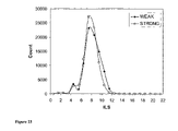
- FIG. 13 Contrast Histogram. This distribution stores the behavior of a particular layout under a predetermined set of optical conditions. The objective of the method is to shift the distribution towards higher values of ILS.
- FIG. 14 Contrast-Distribution for two different illumination pupils.
- off-axis illumination settings such as QuasarTM, improve the image contrast compared to a conventional illumination aperture
- FIG. 17 Scattering Bar parameters. Scattering bar width and separation for optically different edges are calculated to improve depth of focus and feature contrast.
- FIG. 18 Initial and intermediate contrast distributions. Scattering bar insertion can cause very low contrast regions.
- FIG. 19 Initial, intermediate and final contrast distributions.
- the very low contrast regions induced by scattering bars need to be adjusted (in this case erased all together) to prevent contrast degradation.
- FIG. 20 Contrast distributions and weigh functions.
- the weigh function aids in trading high contrast edges for medium contrast edges in order to achieve a more homogeneous imaging.
- FIG. 21 Infocus and defocus evaluation. By improving contrast at best focus conditions, the contrast at out of focus conditions gets improved as well.
- FIG. 22 Initial Contrast Distributions.
- FIG. 22A indicates the initial contrast distribution—C 0 —that will be used to classify edges as being high/low contrast when applying an X dipole single exposure.
- FIG. 22B is the contrast distribution resulting from a Y dipole exposure. Notice how the contrast distributions are not symmetrical. This means that the design is not XY balanced.
- the current example assumes a 50:50 dose split for both masks, but a finer implementation can use this information to determine the best dose split.
- FIG. 23 Initial Double Exposure Contrast Distribution. These distributions are used as reference to the consecutive contrast enhancements that the method proposes. Such a step is necessary to minimize the number of local low contrast cases that a global optimization may suggest.
- FIG. 24 Contrast Distribution after Model Based OPC has been applied to sub-optimal initial masks. Normally strong dipole conditions provide a better pattern resolution, but they also introduce strong proximity effects. These proximity effects are responsible for the loss of contrast in the strong dipole case, which in turn causes the weak dipole illumination system to improve (shifted towards high contrast values).
- FIG. 25 Contrast Distribution of Initial Masks Generated by the Contrast Assisted Dipole Decomposition. These are raw results that do not necessarily meet the pattern resolution criterion. Such a set of masks is used as the initial conditions for a subsequent model-based OPC.
- FIG. 26 Contrast Distribution of Final Masks from the Contrast Based Dipole Decomposition followed by Model Based OPC. From these distributions it is difficult to determine which system will respond better to process variations. While the result from strong dipole conditions has placed more edges in the high contrast category, it has also produced more edges in the lower contrast regions than its weak dipole counterpart.
- FIG. 27 Successive Shift toward Higher Contrast Regions.
- FIG. 27A shows the successive improvement of the method for a weak dipole system.
- FIG. 28 Contrast Distribution Shift due to Defocus Conditions for: A) Strong Dipole Illumination. B) Weak Dipole Illumination.
- FIG. 29 Pattern Fidelity Change due to Defocus and Dose for Strong Dipole Illumination: A) No Contrast-Assisted Method. B) Contrast-Assisted Method.
- Embodiments of the present invention apply resolution enhancing technologies (RETs) to edges of features in photolithographic designs based on contrast classifications of the respective edges to modify the edge's contrast.
- RETs resolution enhancing technologies
- embodiments of the present invention can be applied to a photolithographic design on a global basis to modify the overall contrast of the design.
- Contrast is a direct indication of how well an edge will resolve in a projected image. In which case, contrast classification directly identifies edges that will be most difficult to resolve. Edges with higher contrast appear sharper, allowing for more detailed and smaller feature sizes.
- embodiments of the present invention apply a RET to modify the contrast of the edge and change the slope of the edge's intensity profile.
- a RET to modify the contrast of the edge and change the slope of the edge's intensity profile.
- edges can be placed with more precision, potentially leading to better overall enhancement solutions.
- embodiments of the present invention can sharpen an intensity profile prior to applying OPC so that OPC does not need to move an edge as far it otherwise would.
- embodiments of the present invention can apply virtually any RET that can modify contrast.
- embodiments of the present invention can apply sub-resolution assist features (SRAF), off-axis illumination, di-pole illumination, phase shift mask (PSM), and the like.
- SRAF sub-resolution assist features
- PSM phase shift mask
- edge and edge fragment are interchangeable and refer in general to any segment defining a boundary, or a part of a boundary, of a feature in a photolithographic design.
- One data format commonly used to define such a design is GDSII, in which features comprise collections of interconnected points in two-dimensional space.
- GDSII an edge or edge fragment may comprise a pair of interconnected points in the two-dimensional space.
- FIGS. 5A through 5E illustrate one embodiment of the present invention for global contrast modification.
- the present invention applies a RET to an edge based on the edge fragment's contrast class, thereby modifying the edge's contrast.
- the illustrated embodiment repeatedly applies this operation to multiple edges in a design and explores the overall contrast change for a variety of enhancement options.
- the illustrated embodiment includes a number of implementation-specific details. Other embodiments may not include all of the illustrated operations, may perform the operations in a different order, may combine and/or separate one or more of the operations, and may include additional operations.
- Several functions, curves, graphs, and histograms are mentioned in FIGS. 5A through 5E . Examples of many of these are illustrated in subsequent figures.
- the illustrated embodiment assumes that the optical conditions, such as focus, dose level, numerical aperture, and the like, have already been determined.
- a photolithographic design is fragmented into edges. Fragmenting can be done in a number of different ways and often involves adding additional data points in a design to break up long edges into smaller fragments. With smaller fragments, more accurate and detailed enhancements can be applied, but the trade-off tends to be additional complexity, processing time, etc.
- the process identifies a simulation site in each fragment and calculates an intensity profile for each fragment at the simulation site.
- the calculation can be done in any number of ways.
- the simulation site is at the center of an edge fragment and the intensity profile is calculated along a perpendicular cut line intersecting the edge fragment at the simulation point.
- the calculation may take into consideration features in the design within an area of influence surrounding the simulation site.
- the radius of the area of influence can be selected in any number of ways, but is often related to the optical conditions of the particular system being used. The larger the radius, the more accurate, and time consume, the calculation.
- the process determines the contrast for each edge fragment.
- the illustrated embodiment uses the image log scale (ILS) as an equivalent to contrast.
- ILS image log scale
- One way to calculate the ILS is to take the log of the intensity profile, and determine the maximum derivative of the log function. The derivative is the slope of the function, so the ILS is taken at the maximum slope.
- Other embodiments may calculate contrast in different ways.
- the process tags each edge fragment with a contrast classification depending on the contrast value calculated in 503 .
- a contrast classification depending on the contrast value calculated in 503 .
- that edge is assigned to a contrast classification corresponding to that range.
- Any number of contrast classifications can be used. In general, more classifications and smaller ranges tend to provide more accuracy, but also more complexity.
- operations 502 , 503 , and 504 are all part of the fragmenting operation 501 . That is, in one embodiment, a contrast calculation is performed at regular intervals along each edge in the design. The contrast value at each interval is compared to the ranges of contrast values defined by the contrast classifications. If the contrast value switches from one range to another, the edge is fragmented and the newly formed fragment is tagged with the new contrast classification. This approach is often referred to as model-based fragmenting or model-based tagging.
- the process counts the number of edges that have been tagged with each contrast classification at 505 . For instance, if there are 20 contrast classes, the process will count the number of edges assigned to each of the 20 contrast classes.
- an original contrast signature is formed.
- the original contrast signature is a histogram of fragments versus contrast. For instance, with 20 contrast classes, there will be 20 data points, each plotted as a number of edge fragments in a particular contrast range.
- the process determines a target contrast.
- the target contrast is a minimum desired contrast level.
- the target level can be selected in any number of ways, but is often dependent upon the complexity of the design and the quality of optical system being used.
- the process calculates the number of fragments in the original contrast signature that meet or exceed the target contrast.
- this is simply a matter of adding the numbers of edge fragments in each contrast class that define contrast ranges in excess of the target contrast.
- More complicated systems, with larger numbers of contrast classes may take the integral of the original contrast from the target contrast up to the maximum contrast to determine the area under the curve, with the area being equivalent to the number of edge fragments.
- the process selects a resolution enhancement type.
- This could include selecting a high level RET, such as SRAF, di-pole, PSM, or the like.
- Each of these high level RETs could also include a number of variables from which to select.
- operation 509 could include selecting the spacing between an SRAF and an edge, the width of an SRAF, the number of SRAFs, the spacing separating multiple SRAFs, and the like.
- di-pole or PSM 509 could include selecting, for instance, the distance to which a shield is extended in a second mask to protect an edge in a first mask.
- just one RET, or one variable within a RET can be selected per application of the process. In which case, the process would have to restart in order to select another RET, or another variable within a RET.
- the array of RETs and/or variables from which to choose is limited by factors such as manufacturability, optical conditions, etc. For instance, the width of an SRAF may be fixed in a particular system, so the width variable may not be eligible for selection.
- a contrast classification is selected. As will be seen below, the process will loop back to 510 multiple times until all of the contrast classes have been selected and used by the process.
- the contrast classes can be selected in any order.
- a resolution enhancement value is selected. For instance, where SRAF spacing was chosen back at operation 509 , operation 511 could include selecting a particular spacing value. As will be seen below, if a range of values are available, the process can loop back multiple times to select and use one value at a time until the range values have all been used. In one embodiment, the range of values may be limited by factors such as manufacturability, optical conditions, etc. For instance, the spacing increments for SRAFs may be fixed in a particular system to a certain value, so only certain spacings may be eligible for selection.
- each edge fragment that is assigned to the selected contrast classification is modified with the selected RET and the selected RET value.
- each edge in the selected contrast class may receive an SRAF at a particular spacing and width.
- the process recalculates the contrast (the ILS in this embodiment) for all of the edges, both in the selected contrast class and outside the selected contrast class. Then, the edges are all temporarily retagged to the appropriate contrast classes based on their current contrast values at 514 . At 515 , after the edges have been retagged, the number of edges in each class are counted again to form a current contrast signature comprising a new histogram of fragments versus contrast.
- the illustrated embodiment applies a weight function to the current contrast signature.
- the weight function can be used to emphasize the number of edges having large contrast values so that slight differences are easier to detect in later comparisons, as discussed below. Other embodiments may not use a weight function.
- the process calculates the number of fragments in the current signature that meet or exceed the target contrast. As with the original signature, this operation could include integrating to get the area under the curve. Of course, the weight function can substantially inflate the number of fragments.
- the process calculates a difference between the original number of fragments that exceed the target contrast and the current number of fragments that exceed the target contrast in the current, weighted contrast signature.
- the difference is used as a data point in a cost function curve. Each iteration through the process adds another data point.
- the curve is a function of the difference between the two signatures versus the enhancement value selected at 511 . Different curves will be created with each curve corresponding to a different contrast class.
- the process checks for additional enhancement values. For instance, if a range of SRAF spacings are available, and not all of the spacings have been used yet, the process will loop back to 511 to select another value. The process will loop through 511 to 521 until all of the values have been used. A data point will be added to a curve corresponding to the currently selected contrast class for each pass through 520 . Each iteration will revert back to the original design so that each data point represents the contrast improvement over the original design for just one enhancement applied to just one contrast class.
- the process proceeds to 522 where it checks for additional contrast classes. If at least one additional class remains to be used, the process loops back to 510 to select a new class. The process will iterate through 510 to 522 until all of the contrast classes have been used, and, for each new class, the process will iterate through 511 to 521 for each enhancement value. Each iteration through 522 will create a new cost function curve corresponding to a new contrast class, with a new data point being added to a given cost function curve for each pass through 520 .
- the process proceeds to 523 to select one of the cost function curves.
- the curves can be selected in any order.
- the process identifies a “best” data point in the curve indicating the largest global contrast increase over the original contrast signature while using the smallest resolution enhancement value. That is, if two data points in a curve indicate the same amount of improvement, the data point corresponding to the smaller enhancement value is selected.
- the smaller enhancement value would be the shorting, or closer, spacing value.
- SRAF width the smaller value would be the narrower width.
- the number of SRAFs the smaller value would be the lower number of SRAFs.
- the process checks for additional curves and loops through 523 and 524 until the best data point is identified in each curve. Then, at 526 , the process prioritizes the best data points for each curve, from the data point providing the most global contrast improvement to the data point providing the least contrast improvement.
- the weight function from operation 517 can help.
- the weight function emphasizes the differences between data points to more easily distinguish levels of contrast improvement.
- a tie can be resolved in the priority order by favoring a lower contrast class. That is, if the best data point from two contrast classes provide the same global contrast improvement, it is usually more beneficial to give priority to the lower contrast.
- a resolution enhancement that corresponds to the highest priority data point is selected.
- the selected resolution enhancement is applied to the edge fragments in the original design that are tagged with the respective contrast classification.
- the process checks for additional data points, and loops back to 527 if there is another. In this second iteration, the second highest priority enhancement is applied to the design in addition to the previous enhancement. No single edge receives both enhancements because every edge is assigned to one contrast class, and each contrast class receives only one enhancement. Similarly, the enhancement for the third iteration is applied in addition to the first and second enhancements. The process continues to iterate through 527 to 529 until all of the data points have been used to apply enhancements to the design in the priority order.
- the global contrast signature of the design is likely to have improved substantially.
- the enhancements are evaluated individually by the process, but multiple of enhancements are ultimately applied together with one enhancement per contrast class, the enhancements are likely to conflict and degrade contrast in at least a small number of edges.
- the process selects an edge fragment in the modified design, calculates an intensity profile and contrast for the edge fragment at 531 , and compares the current contrast to the original contrast for that edge.
- the process checks for more fragments at 535 and loops back to 530 for each edge fragment in the design.
- the process does one of two things at 534 . In one embodiment, the process simply removes any enhancement that had been applied to the edge fragment in question. Often times, by removing the enhancement, the edge's contrast will substantially revert back to the original contrast.
- the process can also add the edge to a subset of edges to be re-processed. That is, the entire process of FIGS. 5A through 5E can be repeated, using the design as it was modified in the first pass through the process as the “new” original design.
- the second pass can explore additional enhancements for the subset of problematic edges. For instance, if the process explored SRAF spacing in the first pass, then the second pass could explore SRAF width, or the number of SRAFs, or the process could switch to an entirely different RET.
- the last operation in the process is to apply model-based OPC to the design. Since the process is likely to have improved the edge contrast over much of the design, OPC will generally operate faster and arrive at a superior solution than it otherwise would.
- the process can be restarted and another RET or variable can be selected at 509 .
- Various embodiments of the present invention can be applied to virtually any RET and virtually any variable within a RET.
- the process can be performed twice, once for each expose.
- an original signature can be determined for a horizontal di-pole and enhancements can be explored with respect to the horizontal original signature.
- Another original signature can be determined for a vertical di-pole and enhancements can be explored with respect to it. All of the data points can be compared from both exposures and a best data point can be selected for each contrast class.
- FIGS. 6 through 10 illustrate some examples of the various functions and curves mentioned in FIGS. 5A through 5E .
- a contrast signature 610 is a histogram plotted as a function of the number of edges per contrast value.
- Contrast signature 610 includes edges to either side of target contrast 620 .
- the edges that have acceptable contrasts are those occupying area 630 under the curve 610 and to the right of target contrast 620 .
- the edges to the left of target contrast 620 have unacceptably low contrasts.
- one embodiment of the present invention would start by exploring RETs for the unacceptably low edges.
- Another embodiment of the present invention may only explore RETs for the unacceptably low edges.
- FIG. 7 illustrates one example of a weight function 710 .
- a weighted contrast signature is produced.
- FIG. 8 illustrates one example of a weighted contrast signature 810 .
- the weight function emphasizes the high contrast edges, “magnifying” the area 820 under the curve 810 and to the right of 620 . This magnification can make it easier to recognize the differences between two different cost functions.
- FIG. 9 illustrates one example of a set of cost function curves.
- Each of the curves 910 , 920 , and 930 corresponds to a different contrast classification.
- Each data point in a curve represents the difference between the number of edges with acceptable contrast in the original contrast signature, such as area 630 , and a current weighted, contrast signature, such as area 820 .
- points 911 and 912 provide the same contrast improvement, but point 911 uses a smaller enhancement value. Therefore, point 911 will generally be selected over point 912 .
- both curves 920 and 930 include the same data point 922 . That is, the best data point in both curves provides the same contrast improvement.
- one embodiment of the present invention grants a higher priority to the data point corresponding to the lower contrast classification.
- the enhancement indicated by data point 922 will be applied to the contrast class of curve 930 before the contrast class of curve 920 .
- FIG. 10 illustrates one example where the contrast for some edges is worse after all the enhancements are applied.
- curve 1020 represents the original contrast signature
- curve 1010 represents the contrast signature after all of the enhancements have been applied.
- Curve 1010 includes a “tail” 1030 where the contrast is worse than in the original curve 1020 .
- various embodiments of the present invention may eliminate the enhancements from the edges in tail 1030 , and/or assign those edges to a subset of edges and run them through the process again with a different RET selection.
- FIG. 11 illustrates one embodiment of a hardware system intended to represent a broad category of computer systems such as personal computers, workstations, and/or embedded systems.
- the hardware system includes processor 1110 coupled to high speed bus 1105 , which is coupled to input/output (I/O) bus 1115 through bus bridge 1130 .
- Temporary memory 1120 is coupled to bus 1105 .
- Permanent memory 1140 is coupled to bus 1115 .
- I/O device(s) 1150 is also coupled to bus 1115 .
- I/O device(s) 1150 may include a display device, a keyboard, one or more external network interfaces, etc.
- temporary memory 1120 may be on-chip with processor 1110 .
- permanent memory 1140 may be eliminated and temporary memory 1120 may be replaced with an electrically erasable programmable read only memory (EEPROM), wherein software routines are executed in place from the EEPROM.
- EEPROM electrically erasable programmable read only memory
- Some implementations may employ a single bus, to which all of the components are coupled, or one or more additional buses and bus bridges to which various additional components can be coupled.
- Those skilled in the art will be familiar with a variety of alternate internal networks including, for instance, an internal network based on a high speed system bus with a memory controller hub and an I/O controller hub.
- Additional components may include additional processors, a CD ROM drive, additional memories, and other peripheral components known in the art.
- the present invention is implemented using one or more hardware systems such as the hardware system of FIG. 11 .
- the systems can be coupled to communicate over an external network, such as a local area network (LAN), an internet protocol (IP) network, etc.
- the present invention is implemented as software routines executed by one or more execution units within the computer(s).
- the software routines can be stored on a storage device, such as permanent memory 1140 .
- the software routines can be machine executable instructions 1210 stored using any machine readable storage medium 1220 , such as a diskette, CD-ROM, magnetic tape, digital video or versatile disk (DVD), laser disk, ROM, Flash memory, etc.
- the series of instructions need not be stored locally, and could be received from a remote storage device, such as a server on a network, a CD ROM device, a floppy disk, etc., through, for instance, I/O device(s) 1150 of FIG. 11 .
- the instructions may be copied from the storage device into temporary memory 1120 and then accessed and executed by processor 1110 .
- these software routines are written in the C programming language. It is to be appreciated, however, that these routines may be implemented in any of a wide variety of programming languages.
- the present invention is implemented in discrete hardware or firmware.
- one or more application specific integrated circuits ASICs
- one or more functions of the present invention could be implemented in one or more ASICs on additional circuit boards and the circuit boards could be inserted into the computer(s) described above.
- field programmable gate arrays FPGAs
- SPGA static programmable gate arrays
- a combination of hardware and software could be used to implement one or more functions of the present invention.
- RET resolution enhancement technique
- the method is based on extracting a distribution of the image log slope (ILS) for a given layout under a predefined set of optical conditions. This distribution is then taken as the optical signature for the image local contrast of the design.
- the optical signature can be created for an entire layout, or only for certain cells believed to be problematic. Comparisons can be made between the optical signatures generated using different illumination/RET strategies.
- SRAF sub-resolution assist features
- double exposure dipole illumination double exposure dipole illumination.
- Pattern Fidelity is related to the design—stored in a layout as polygonal shapes—that must be transferred to a given substrate preserving the intended functionality of the devices.
- Image transfer robustness as important as the first, has been studied in great detail, giving birth to the notion of common process window. If the image-transfer can only be reproduced under a very limited set of dose and exposure conditions—a small process window—, the process cannot be implemented in the real world, where small variations are always present and difficult to control at the level of precision required with current hardware.
- Pattern fidelity has normally been addressed by first generation OPC (rule v and model based 1, vi, vii ). These methods do not generate additional polygons in the layout, but typically only move existing edges to achieve a given pattern fidelity.
- Second generation approaches add new features to the design in various ways. viii,ix For example, sub-resolution assist features (SRAF) are additional non-printing structures placed parallel to original edges in various ways. x They are typically inserted to allow isolated features to diffract light like dense features, reducing the Iso/Dense bias that can be a common lithographic problem.
- SRAF sub-resolution assist features
- Geometric rule-based approaches can return acceptable results when it is possible to distinguish how a particular feature will behave optically from purely geometric arguments. This is especially true in the traditional lithography (k 1 >0.7) where feature-size and feature separation correlate well with contrast and other optical quantities. However in the deep sub-wavelength regime there are many instances in which the optical environment changes the optical behavior of geometrically equivalent features (e.g. critical features close to landing pads, 45° edges or low aspect ratio structures).
- the method that we propose here classifies edges based on their own optical behavior. By using this approach, it is possible to generate masks that return a higher contrast image with acceptable edge placement error.
- the key parameter for classification is not based on EPE, as determined from the local image intensity, but based on local image contrast, as determined from the image log-slope (ILS). Optimization of the layout patterns for OPC is therefore not calculated by minimizing EPE, but my maximizing local contrast. Yet, OPC is needed in order to attain the target CD. By combining an RET optimization and OPC, the layout is closer to meet the robustness and resolution criteria required to any process worthy technology.
- contrast ( d ln ⁇ ⁇ I d x ) max ( 1 )
- I aerial image intensity
- x length
- NILS Normalized Image Log-Slope
- CD Critical Dimension (Line width)
- I Intensity
- x Length
- the determination of image contrast is a calculation very similar to that needed to determine EPE, and does not require significant additional computation time.
- the derivative of the image intensity can be easily calculated once the image of a layout has been simulated. Since it is very difficult to visualize every edge in a layout tool, aggregations of data can be conveniently presented in histograms, just as histograms of EPE can be used to evaluate pattern fidelity.
- the histogram represents the distribution of contrast values found throughout the image, with one “count” occurring for each contrast value (or ILS) uniquely assigned to each edge segment. This histogram corresponds to the optical signature of a particular layout under a predetermined set of optical conditions.
- FIG. 13 is an example of such a histogram.
- no RET or OPC has been applied to the layout, meaning that this contrast distribution is a reference point for our subsequent simulations after the application of various RETs.
- the total number of segments in a histogram should be constant when evaluating the same layout. This conservation principle has been used consistently in all simulations performed.
- H RET can represent many things, depending on the RET conditions applied, and is a function dependent on many, many variables. There is therefore an actual family of histograms, ⁇ H i RET ⁇ depending on a particular variable that is changed.
- ⁇ H i RET ⁇ depending on a particular variable that is changed.
- the spacing of the SRAF is a critical parameter that requires optimization.
- the orthogonal edge bias becomes another key parameter to explore. Even optical parameters such as sigma and other pupil dependent quantities can be explored using this approach.
- a cost function ⁇ is generated as a function of the RET technique and the key parameter ⁇ under optimization. This represents the subtraction of sub-optimal contrast counts from the number of counts at acceptable contrast.
- C i C max ⁇ ⁇ H RET ⁇ ( ⁇ , C o , C i )
- ⁇ C i C min
- C i C T ⁇ ⁇ H RET ⁇ ( ⁇ , C o , C i ) ( 3 )
- This technique can be further adapted by the addition of a weighting function.
- maximization of ⁇ above will produce a higher contrast image, some edges with extremely low contrast may have low values of H RET , but even a single failure in the wrong place can cause an IC to fail.
- a weighting function W can be introduced.
- W can take any form. Typically, W can be high for values of low contrast and 1 for acceptable values. W can also be defined a parabola, centered on C T . By selecting different W functional forms, it is possible to trade areas of high contrast with areas of very low contrast. Experimentation with various weighting functions that produce better wafer results is still an active area of investigation.
- the resulting layout is evaluated to assess the improvement in overall contrast of the design.
- a direct model-based solution guarantees that the given layout will have an acceptable pattern fidelity
- a combination of contrast optimization and model-based OPC returns the same level of confidence from the pattern fidelity point of view, plus the added advantage of a higher contrast layout less sensitive to dose and focus variations.
- FIG. 15 shows how the cost function ⁇ can be used to determine the best opening angle for an off-axis illumination system, from the image contrast viewpoint.
- the value of ⁇ for the conventional case is included for reference.
- FIG. 16 explores how the contrast changes by adjusting the inner sigma and keeping the opening at 30° and the outer sigma at 0.875. According to these results, the best illumination pupil will be a 30° Quasar illumination, with outer sigma of 0.875 and inner sigma of 0.05.
- this information suggests the range of settings that will provide adequate imaging from the contrast point of view.
- Sub resolution assist features have been used for some time as a rule-based technique for OPC that reduces iso-dense bias and increases contrast and process window.
- xvii , xviii An illustration of a generic SRAF is shown in FIG. 17 .
- All the parameters that define an assist feature rule have unique advantages and limitations.
- Current mask manufacturing processes can control the width of individual SRAF across the full design, as long as the target width is constant, and the distance between bars depends on the pattern recognition capabilities of current inspection tools.
- SRAF-to-main feature separation alters the contrast of the original edges without creating many problems during the mask manufacturing process so long as the separation lies within the current mask manufacturing and inspection constraints.
- FIG. 18 shows that the thoughtless application of SRAF by a simple rule can generate few cases with an even lower contrast value. Such cases are later translated in poor resolution regions where killer defects (such as bridging or pinching) can occur.
- FIG. 19 shows three different curves: the original contrast distribution (solid line), the distribution immediately after global optimization (dashed line with clear squares) and the final contrast distribution after local correction (solid line and solid squares). After final cleanup, there are no cases of lower-than-original-contrast edges. These regions have in fact been found previously xx and they depend on the set of optical conditions that are used. xx R. Socha, et al. “Forbidden Pitches for 130 nm lithography and below”, Proc. SPIE Vol.4000, 1140–1155 (2000),
- W - 2.79 ⁇ ILS + 30.854 [ 0 , 11 ]
- W 1 ( 11 , 13 ]
- W 2.55 ⁇ ILS - 32.703 ( 13 , ⁇ ) ( 5 )
- Equation 5 weighs low-ILS values more (ILS from 0 to 11 are considered low in this example, but the range depends on the specific process requirements), which in turn returns a smaller cost ( ⁇ ).
- SRAF and many other Resolution Enhancement Techniques is to improve the process window of a particular design. So far we have focused on the importance of improving contrast. However, as FIG. 21 indicates, by maximizing contrast it is possible to increase the process window of the design without having to simulate a large set of different dose and focus conditions.
- FIG. 21 shows 4 curves: The original contrast distribution at best focus (solid line), the final contrast distribution at best focus (solid line with square markers), the original layout with no OPC at 0.3 micron defocus (dashed lines) and the layout with the SRAF calculated from the in-focus case but simulated at 0.3 micron defocus (dashed lines and solid squares).
- This very simple method is able to increase the number of cases that can be found closer to higher contrast (and therefore more robust imaging) regions. Since some SRAF were completely removed, the out-of-focus distributions are very similar to each other at low contrast values.
- RET that has recently been considered for the 65 nm node is dipole illumination.
- the resolution enhancement potential was originally recognized over 10 years ago, xxi it was quickly realized that double exposures would be required to make a complete image, in which vertical lines are printed with a horizontal dipole and horizontal lines are printed with a vertical dipole.
- xxii Dipole was abandoned for more generally applicable, single exposure techniques like model-based OPC.
- xxi S. Asai, I. Hanyu, and K. Hikosaka “Improving projection lithography image illumination by using sources far from the optical axis”, J. Vac. Sci Technol B9 2788–2791 (1991).
- xxii S. Asai, I. Hanyu, and K. Hikosaka “High performance optical lithography using a separated light source”, J. Vac. Sci Technol B10 3023–3026 (1991).
- the range that results from the sum of both ranges (3,15) creates the set of candidates for the ILS value that will be used to decide if a feature has low or high contrast and therefore in which mask it should be controlled.
- We have arbitrarily chosen an ILS 10 since it is located in the upper half portion of the range, but further optimization may be needed in order to define the best ILS value to make such edge selection.
- FIG. 23 is the lower limit of the method. Only one mask is used for both exposures. Under weak dipole conditions the distribution is slightly shifted toward higher contrast values with respect to the strong dipole case. This has to do with the strong proximity and 0 th order light that degrade the final pattern during the non-optimal exposure step. The successive improvement in contrast is compared to this limiting case in order to prevent situations where the method proposes a solution that may very well improve the global contrast, but can locally generate low contrast regions that translate in possible sites for line pinching or bridging defects.
- a double exposure model-based OPC requires three layers as input: A target layer that corresponds to the intended design, and one layer for each exposure. By manipulating the edges present in both masks the method converges to a solution that attains the correct pattern fidelity specified by the target layer. There are many possible solutions to the problem, especially when the design needs to be split into two or more exposures. It is possible in principle to feed the original design three times to the model-based OPC method (as the target design, and as the first and second exposure masks). The method will converge to a solution that returns acceptable pattern fidelity for that specific set of conditions.
- FIG. 24 shows the final contrast distributions after this approach has been used. Both distributions are shifted towards higher contrast values with respect to the lower limiting case presented in FIG. 23 . FIG. 24 shows the distributions that the contrast-based method will now use as reference for improvement.
- FIG. 25 shows the contrast distributions for the weak and strong dipole conditions.
- the final contrast distributions that result from the contrast assisted decomposition and the model-based OPC are not necessarily narrower than the distributions obtained from applying model-based OPC to a sub-optimal initial set of masks. Since this is not a critical dimension (CD) distribution, the spreading of the distributions towards higher values of contrast is in fact more desirable than a narrow contrast distribution centered on a lower contrast region.
- FIG. 26 shows the contrast distributions that result from the combined use of a model assisted decomposition and a model based OPC.
- FIG. 27 shows the incremental shift of the final contrast distributions for two systems: 15 A for weak dipole conditions and 15 B for strong dipole conditions.
- Such masks have distributions (dark continuous line) that have already shifted to higher contrast values as determined by the method. These masks very likely do not meet the pattern fidelity constraints. Because of that, they are only used as initial conditions for the model-based OPC correction. Once this final model-based OPC has been applied to the masks generated by the contrast-assisted method; a new distribution, generally better than all previously calculated cases, is obtained (light continuous line).
- the goal is to improve the overall process window of a particular design.
- FIG. 28 shows how the solution calculated at best focus responds with varying focus.
- the light lines highlight the system that was not subject to dipole decomposition, while the dark lines indicate the distributions for the set of masks that received a contrast-assisted decomposition. It is expected that the best method should prevent large variations of contrast for every edge in the design.
- FIG. 28A shows that for the strong dipole condition, the contrast-based method does not shift as far as in the case where no special decomposition was used.
- the area defined by the overlap between the distributions calculated at different focus conditions is larger and centered towards higher values of contrast when the contrast-assisted decomposition is used.
- Pattern fidelity is difficult to account for.
- one dimensional process windows have been used to rank the feasibility of a particular process.
- such metrics do not necessarily capture the two-dimensional aspects present in any real design.
- a statistical evaluation of the patterns can be performed as described in detail elsewhere xxiii . In this case we have decided to select a specific region of the design under study and simulate its optical behavior at two foci conditions and three different reduced threshold values (0.18, 0.20, 0.22).
- xxiii L. Capodieci J. A. Torres, et. al. “Effects of advanced illumination schemes on design manufacturability and interactions with optical proximity corrections”. Proc. SPIE Vol. 4181, 58–60 (2001)
- the area of simulation depicted in FIG. 29 indicates that at zero defocus conditions the system has perfect pattern fidelity, including 45° angles and low aspect ratio segments. However, when the conditions are other than the ones used for simulation (e.g. at 0.3 ⁇ m defocus), different killer defects can be found.
- the circles highlight regions at which there has been strong pattern fidelity degradation.
- the solution from the contrast-assisted decomposition method behaves in a much better fashion than when the contrast-assisted solution is subject to the same threshold (dose) and focus variations.
- dose dose
- focus variations the variations highlighted in FIG. 29B (at 0.3 microns defocus) are not as large as in the previously described case—the method can further be improved by including additional features that can minimize the apparent iso-dense bias. While sub-resolution assist features were not used in this case, they can be added to the mask following the same contrast enhancement criteria used to determine the optimal bias values. It is also important to mention that at the end of this process, all the regions that present problems are already identified, reducing the number of edges that need to be inspected and fixed later on.
- the method proposed here maximizes the local contrast for every edge, as defined by the image log-slope (ILS). While we believe that this metric captures the essential behavior related to image local contrast, there is no data that suggests that similar results cannot be achieved or improved by different local contrast-related functional forms.
- ILS image log-slope
- a complete and integrated approach can accept further restrictions, since the method can often be misused to generate acceptable RET recipes from the local contrast point of view, but completely unacceptable results from the pattern fidelity viewpoint. If mask-manufacturing constraints can be relaxed, the current approach is able to further adjust other geometric parameters that define a complete RET recipe. It is possible to do so as long as the changes do not become first order.
Abstract
Description
Where C is Contrast, I is aerial image intensity, x is length.
Where, CD=Critical Dimension (Line width), I=Intensity, x=Length
By maximizing this function, a more printable image is achieved.
W can take any form. Typically, W can be high for values of low contrast and 1 for acceptable values. W can also be defined a parabola, centered on CT. By selecting different W functional forms, it is possible to trade areas of high contrast with areas of very low contrast. Experimentation with various weighting functions that produce better wafer results is still an active area of investigation.
This way, the final solution is biased towards higher contrast values. Notice how the functional form of both distributions is essentially the same; only the peaks and valleys are slightly different. The distribution that results from using an improved weighing function is clearly better since it generates more high contrast edges. The addition of weights to the distributions is a global control of the allowed tradeoffs between low, nominal and high ILS values.
Claims (21)
Priority Applications (4)
| Application Number | Priority Date | Filing Date | Title |
|---|---|---|---|
| US10/356,382 US7013439B2 (en) | 2002-01-31 | 2003-01-31 | Contrast based resolution enhancing technology |
| US10/888,444 US7293249B2 (en) | 2002-01-31 | 2004-07-09 | Contrast based resolution enhancement for photolithographic processing |
| US11/669,100 US7562336B2 (en) | 2002-01-31 | 2007-01-30 | Contrast based resolution enhancement for photolithographic processing |
| US12/501,349 US8108806B2 (en) | 2002-01-31 | 2009-07-10 | Contrast-based resolution enhancement for photolithographic processing |
Applications Claiming Priority (3)
| Application Number | Priority Date | Filing Date | Title |
|---|---|---|---|
| US35404202P | 2002-01-31 | 2002-01-31 | |
| US36069202P | 2002-02-28 | 2002-02-28 | |
| US10/356,382 US7013439B2 (en) | 2002-01-31 | 2003-01-31 | Contrast based resolution enhancing technology |
Related Child Applications (1)
| Application Number | Title | Priority Date | Filing Date |
|---|---|---|---|
| US10/888,444 Continuation-In-Part US7293249B2 (en) | 2002-01-31 | 2004-07-09 | Contrast based resolution enhancement for photolithographic processing |
Publications (2)
| Publication Number | Publication Date |
|---|---|
| US20040005089A1 US20040005089A1 (en) | 2004-01-08 |
| US7013439B2 true US7013439B2 (en) | 2006-03-14 |
Family
ID=30003768
Family Applications (1)
| Application Number | Title | Priority Date | Filing Date |
|---|---|---|---|
| US10/356,382 Expired - Lifetime US7013439B2 (en) | 2002-01-31 | 2003-01-31 | Contrast based resolution enhancing technology |
Country Status (1)
| Country | Link |
|---|---|
| US (1) | US7013439B2 (en) |
Cited By (34)
| Publication number | Priority date | Publication date | Assignee | Title |
|---|---|---|---|---|
| US20040209176A1 (en) * | 2002-06-11 | 2004-10-21 | Numerical Technologies, Inc. | Model-based data conversion |
| US20050251771A1 (en) * | 2004-05-07 | 2005-11-10 | Mentor Graphics Corporation | Integrated circuit layout design methodology with process variation bands |
| US20050268272A1 (en) * | 2003-12-18 | 2005-12-01 | Lsi Logic Corporation | Method and apparatus for optimizing fragmentation of boundaries for optical proximity correction (OPC) purposes |
| US20060188673A1 (en) * | 2005-02-24 | 2006-08-24 | Melvin Lawrence S Iii | Method and apparatus for determining an improved assist feature configuration in a mask layout |
| US20060200790A1 (en) * | 2005-03-02 | 2006-09-07 | Shang Shumay D | Model-based SRAF insertion |
| US20060281016A1 (en) * | 2005-06-10 | 2006-12-14 | Texas Instruments Incorporated | Modifying sub-resolution assist features according to rule-based and model-based techniques |
| US20070026322A1 (en) * | 2005-08-01 | 2007-02-01 | Chin-Cheng Yang | Integration system and the method for operating the same |
| US20070031740A1 (en) * | 2005-06-22 | 2007-02-08 | Chen Jang F | Method, program product and apparatus for performing mask feature pitch decomposition for use in a multiple exposure process |
| US20070042277A1 (en) * | 2002-11-12 | 2007-02-22 | Asml Masktools B.V. | Method and apparatus for performing model-based layout conversion for use with dipole illumination |
| US20070118826A1 (en) * | 2004-06-02 | 2007-05-24 | Lippincott George P | Opc conflict identification and edge priority system |
| US20070124708A1 (en) * | 2002-01-31 | 2007-05-31 | Torres Robles Juan A | Contrast based resolution enhancement for photolithographic processing |
| US20070198967A1 (en) * | 2006-02-17 | 2007-08-23 | Zhuoxiang Ren | Computation of electrical properties of an ic layout |
| US20070277145A1 (en) * | 2006-05-26 | 2007-11-29 | International Business Machines Corporation | Iterative method for refining integrated circuit layout using compass optical proximity correction (opc) |
| US20080022240A1 (en) * | 2006-05-17 | 2008-01-24 | Shigeki Nojima | Pattern data verification method for semiconductor device, computer-readable recording medium having pattern data verification program for semiconductor device recorded, and semiconductor device manufacturing method |
| US20080037858A1 (en) * | 2003-10-27 | 2008-02-14 | International Business Machines Corporation | Simultaneous computation of multiple points on one or multiple cut lines |
| US20080054392A1 (en) * | 2006-08-29 | 2008-03-06 | International Business Machines Corporation | Bridge for semiconductor internal node |
| US20080118852A1 (en) * | 2006-11-21 | 2008-05-22 | Cadence Design Systems, Inc. | Method and System for Lithography Simulation and Measurement of Critical Dimensions with Improved CD Marker Generation and Placement |
| US20080141195A1 (en) * | 2006-11-09 | 2008-06-12 | Juan Andres Torres Robles | Analysis optimizer |
| US20080148217A1 (en) * | 2006-12-13 | 2008-06-19 | Jea-Woo Park | Selective shielding for multiple exposure masks |
| US20080166639A1 (en) * | 2007-01-08 | 2008-07-10 | Jea-Woo Park | Data preparation for multiple mask printing |
| US20080195996A1 (en) * | 2007-02-09 | 2008-08-14 | Juan Andres Torres Robles | Pre-bias optical proximity correction |
| US20080193859A1 (en) * | 2007-02-09 | 2008-08-14 | Ayman Yehia Hamouda | Dual metric opc |
| US20080203518A1 (en) * | 2007-02-26 | 2008-08-28 | Nagaraj Savithri | Method for positioning sub-resolution assist features |
| US20080254633A1 (en) * | 2007-04-10 | 2008-10-16 | International Business Machines Corporation | Multiple exposure lithography method incorporating intermediate layer patterning |
| US7448012B1 (en) * | 2004-04-21 | 2008-11-04 | Qi-De Qian | Methods and system for improving integrated circuit layout |
| US20090100389A1 (en) * | 2007-10-11 | 2009-04-16 | Ir Kusnadi | Shape-based photolithographic model calibration |
| US20090121357A1 (en) * | 2007-11-08 | 2009-05-14 | International Business Machines Corporation | Design structure for bridge of a seminconductor internal node |
| US20100023897A1 (en) * | 2008-02-20 | 2010-01-28 | Pikus Fedor G | Property-Based Classification In Electronic Design Automation |
| US20100229133A1 (en) * | 2009-03-03 | 2010-09-09 | Pikus Fedor G | Property-Based Classification In Electronic Design Automation |
| US20100318956A1 (en) * | 2009-06-11 | 2010-12-16 | International Business Machines Corporation | Method of integrated circuit chip fabrication and program product therefor |
| US8713483B2 (en) | 2007-06-05 | 2014-04-29 | Mentor Graphics Corporation | IC layout parsing for multiple masks |
| US20140264773A1 (en) * | 2013-03-15 | 2014-09-18 | Taiwan Semiconductor Manufacturing Company, Ltd. | System and method for optimization of an imaged pattern of a semiconductor device |
| US8856695B1 (en) * | 2013-03-14 | 2014-10-07 | Samsung Electronics Co., Ltd. | Method for generating post-OPC layout in consideration of top loss of etch mask layer |
| US8910098B1 (en) * | 2014-02-18 | 2014-12-09 | Mentor Graphics Corporation | Neighbor-aware edge fragment adjustment for optical proximity correction |
Families Citing this family (31)
| Publication number | Priority date | Publication date | Assignee | Title |
|---|---|---|---|---|
| US6425113B1 (en) * | 2000-06-13 | 2002-07-23 | Leigh C. Anderson | Integrated verification and manufacturability tool |
| US7412676B2 (en) * | 2000-06-13 | 2008-08-12 | Nicolas B Cobb | Integrated OPC verification tool |
| US6887633B2 (en) * | 2002-02-08 | 2005-05-03 | Chih-Hsien Nail Tang | Resolution enhancing technology using phase assignment bridges |
| US6928634B2 (en) * | 2003-01-02 | 2005-08-09 | Yuri Granik | Matrix optical process correction |
| US6978438B1 (en) * | 2003-10-01 | 2005-12-20 | Advanced Micro Devices, Inc. | Optical proximity correction (OPC) technique using generalized figure of merit for photolithograhic processing |
| US7463774B2 (en) * | 2004-01-07 | 2008-12-09 | Microsoft Corporation | Global localization by fast image matching |
| US7861207B2 (en) | 2004-02-25 | 2010-12-28 | Mentor Graphics Corporation | Fragmentation point and simulation site adjustment for resolution enhancement techniques |
| US20050202326A1 (en) * | 2004-03-09 | 2005-09-15 | International Business Machines Corporation | Optimized placement of sub-resolution assist features within two-dimensional environments |
| US7080349B1 (en) * | 2004-04-05 | 2006-07-18 | Advanced Micro Devices, Inc. | Method of developing optimized optical proximity correction (OPC) fragmentation script for photolithographic processing |
| US6977715B2 (en) * | 2004-05-19 | 2005-12-20 | Nanya Technology Corp. | Method for optimizing NILS of exposed lines |
| US7522779B2 (en) * | 2004-06-30 | 2009-04-21 | Accuray, Inc. | Image enhancement method and system for fiducial-less tracking of treatment targets |
| US8304180B2 (en) * | 2004-09-14 | 2012-11-06 | Asml Netherlands B.V. | Lithographic apparatus and device manufacturing method |
| US7493587B2 (en) * | 2005-03-02 | 2009-02-17 | James Word | Chromeless phase shifting mask for integrated circuits using interior region |
| US7434199B2 (en) * | 2005-09-27 | 2008-10-07 | Nicolas Bailey Cobb | Dense OPC |
| US7325225B2 (en) * | 2005-10-05 | 2008-01-29 | Yasushi Tanaka | Method and apparatus for reducing OPC model errors |
| US7506285B2 (en) | 2006-02-17 | 2009-03-17 | Mohamed Al-Imam | Multi-dimensional analysis for predicting RET model accuracy |
| EP2267530A1 (en) * | 2006-04-06 | 2010-12-29 | ASML MaskTools B.V. | Method and apparatus for performing dark field double dipole lithography |
| US7562337B2 (en) * | 2006-12-11 | 2009-07-14 | International Business Machines Corporation | OPC verification using auto-windowed regions |
| US8713488B2 (en) * | 2007-02-28 | 2014-04-29 | Mentor Graphics Corporation | Layout design defect repair based on inverse lithography and traditional optical proximity correction |
| US8971658B2 (en) * | 2007-04-23 | 2015-03-03 | Xerox Corporation | Edge contrast adjustment filter |
| US8028252B2 (en) | 2007-09-14 | 2011-09-27 | Luminescent Technologies Inc. | Technique for determining mask patterns and write patterns |
| US8572517B2 (en) * | 2008-06-10 | 2013-10-29 | Cadence Design Systems, Inc. | System and method for modifying a data set of a photomask |
| US20100064274A1 (en) * | 2008-09-05 | 2010-03-11 | Qimonda Ag | Proximity correction method and system |
| US8250495B2 (en) * | 2009-01-16 | 2012-08-21 | Mentor Graphics Corporation | Mask decomposition for double dipole lithography |
| US8837857B2 (en) * | 2009-04-09 | 2014-09-16 | National Ict Australia Limited | Enhancing image data |
| JP5312166B2 (en) * | 2009-04-13 | 2013-10-09 | キヤノン株式会社 | Image processing apparatus, control method, and program |
| US8887106B2 (en) * | 2011-12-28 | 2014-11-11 | Taiwan Semiconductor Manufacturing Company, Ltd. | Method of generating a bias-adjusted layout design of a conductive feature and method of generating a simulation model of a predefined fabrication process |
| US9355201B2 (en) | 2012-08-17 | 2016-05-31 | Mentor Graphics Corporation | Density-based integrated circuit design adjustment |
| AU2016374520C1 (en) * | 2015-12-14 | 2020-10-15 | Motion Metrics International Corp. | Method and apparatus for identifying fragmented material portions within an image |
| TWI745351B (en) * | 2017-02-24 | 2021-11-11 | 聯華電子股份有限公司 | Method for decomposing semiconductor layout pattern |
| US10426424B2 (en) | 2017-11-21 | 2019-10-01 | General Electric Company | System and method for generating and performing imaging protocol simulations |
Citations (24)
| Publication number | Priority date | Publication date | Assignee | Title |
|---|---|---|---|---|
| US4762396A (en) | 1985-11-21 | 1988-08-09 | Dumant Jean M | Masking method |
| US5502654A (en) | 1993-10-29 | 1996-03-26 | Nec Corporation | Method for analyzing light intensity distribution in projection systems |
| US5655110A (en) | 1995-02-13 | 1997-08-05 | Advanced Micro Devices, Inc. | Method for setting and adjusting process parameters to maintain acceptable critical dimensions across each die of mass-produced semiconductor wafers |
| JPH09319067A (en) | 1995-12-22 | 1997-12-12 | Toshiba Corp | Method for correcting optical proximity effect |
| US5723233A (en) | 1996-02-27 | 1998-03-03 | Lsi Logic Corporation | Optical proximity correction method and apparatus |
| US5825647A (en) | 1995-03-13 | 1998-10-20 | Sony Corporation | Correction method and correction apparatus of mask pattern |
| US6016357A (en) | 1997-06-16 | 2000-01-18 | International Business Machines Corporation | Feedback method to repair phase shift masks |
| US6049660A (en) | 1996-12-27 | 2000-04-11 | Hyundai Electronics Industries Co., Ltd. | Simulation method in lithographic process |
| US6120952A (en) | 1998-10-01 | 2000-09-19 | Micron Technology, Inc. | Methods of reducing proximity effects in lithographic processes |
| US6128067A (en) | 1998-04-28 | 2000-10-03 | Kabushiki Kaisha Toshiba | Correcting method and correcting system for mask pattern |
| US6187483B1 (en) | 1999-05-28 | 2001-02-13 | Advanced Micro Devices, Inc. | Mask quality measurements by fourier space analysis |
| US6243855B1 (en) | 1997-09-30 | 2001-06-05 | Kabushiki Kaisha Toshiba | Mask data design method |
| US6249904B1 (en) | 1999-04-30 | 2001-06-19 | Nicolas Bailey Cobb | Method and apparatus for submicron IC design using edge fragment tagging to correct edge placement distortion |
| US6263299B1 (en) | 1999-01-19 | 2001-07-17 | Lsi Logic Corporation | Geometric aerial image simulation |
| US6269472B1 (en) | 1996-02-27 | 2001-07-31 | Lsi Logic Corporation | Optical proximity correction method and apparatus |
| WO2001065315A2 (en) | 2000-02-28 | 2001-09-07 | Numerical Technologies, Inc. | Method and apparatus for mixed-mode optical proximity correction |
| US6301697B1 (en) | 1999-04-30 | 2001-10-09 | Nicolas B. Cobb | Streamlined IC mask layout optical and process correction through correction reuse |
| US6370679B1 (en) | 1997-09-17 | 2002-04-09 | Numerical Technologies, Inc. | Data hierarchy layout correction and verification method and apparatus |
| US6425117B1 (en) | 1995-03-06 | 2002-07-23 | Lsi Logic Corporation | System and method for performing optical proximity correction on the interface between optical proximity corrected cells |
| US6453457B1 (en) | 2000-09-29 | 2002-09-17 | Numerical Technologies, Inc. | Selection of evaluation point locations based on proximity effects model amplitudes for correcting proximity effects in a fabrication layout |
| US6453452B1 (en) | 1997-12-12 | 2002-09-17 | Numerical Technologies, Inc. | Method and apparatus for data hierarchy maintenance in a system for mask description |
| US6467076B1 (en) | 1999-04-30 | 2002-10-15 | Nicolas Bailey Cobb | Method and apparatus for submicron IC design |
| US6499003B2 (en) | 1998-03-03 | 2002-12-24 | Lsi Logic Corporation | Method and apparatus for application of proximity correction with unitary segmentation |
| US6601231B2 (en) * | 2001-07-10 | 2003-07-29 | Lacour Patrick Joseph | Space classification for resolution enhancement techniques |
-
2003
- 2003-01-31 US US10/356,382 patent/US7013439B2/en not_active Expired - Lifetime
Patent Citations (26)
| Publication number | Priority date | Publication date | Assignee | Title |
|---|---|---|---|---|
| US4762396A (en) | 1985-11-21 | 1988-08-09 | Dumant Jean M | Masking method |
| US5502654A (en) | 1993-10-29 | 1996-03-26 | Nec Corporation | Method for analyzing light intensity distribution in projection systems |
| US5655110A (en) | 1995-02-13 | 1997-08-05 | Advanced Micro Devices, Inc. | Method for setting and adjusting process parameters to maintain acceptable critical dimensions across each die of mass-produced semiconductor wafers |
| US6425117B1 (en) | 1995-03-06 | 2002-07-23 | Lsi Logic Corporation | System and method for performing optical proximity correction on the interface between optical proximity corrected cells |
| US5825647A (en) | 1995-03-13 | 1998-10-20 | Sony Corporation | Correction method and correction apparatus of mask pattern |
| JPH09319067A (en) | 1995-12-22 | 1997-12-12 | Toshiba Corp | Method for correcting optical proximity effect |
| US5879844A (en) | 1995-12-22 | 1999-03-09 | Kabushiki Kaisha Toshiba | Optical proximity correction method |
| US6077310A (en) | 1995-12-22 | 2000-06-20 | Kabushiki Kaisha Toshiba | Optical proximity correction system |
| US6269472B1 (en) | 1996-02-27 | 2001-07-31 | Lsi Logic Corporation | Optical proximity correction method and apparatus |
| US5723233A (en) | 1996-02-27 | 1998-03-03 | Lsi Logic Corporation | Optical proximity correction method and apparatus |
| US6049660A (en) | 1996-12-27 | 2000-04-11 | Hyundai Electronics Industries Co., Ltd. | Simulation method in lithographic process |
| US6016357A (en) | 1997-06-16 | 2000-01-18 | International Business Machines Corporation | Feedback method to repair phase shift masks |
| US6370679B1 (en) | 1997-09-17 | 2002-04-09 | Numerical Technologies, Inc. | Data hierarchy layout correction and verification method and apparatus |
| US6243855B1 (en) | 1997-09-30 | 2001-06-05 | Kabushiki Kaisha Toshiba | Mask data design method |
| US6453452B1 (en) | 1997-12-12 | 2002-09-17 | Numerical Technologies, Inc. | Method and apparatus for data hierarchy maintenance in a system for mask description |
| US6499003B2 (en) | 1998-03-03 | 2002-12-24 | Lsi Logic Corporation | Method and apparatus for application of proximity correction with unitary segmentation |
| US6128067A (en) | 1998-04-28 | 2000-10-03 | Kabushiki Kaisha Toshiba | Correcting method and correcting system for mask pattern |
| US6120952A (en) | 1998-10-01 | 2000-09-19 | Micron Technology, Inc. | Methods of reducing proximity effects in lithographic processes |
| US6263299B1 (en) | 1999-01-19 | 2001-07-17 | Lsi Logic Corporation | Geometric aerial image simulation |
| US6301697B1 (en) | 1999-04-30 | 2001-10-09 | Nicolas B. Cobb | Streamlined IC mask layout optical and process correction through correction reuse |
| US6249904B1 (en) | 1999-04-30 | 2001-06-19 | Nicolas Bailey Cobb | Method and apparatus for submicron IC design using edge fragment tagging to correct edge placement distortion |
| US6467076B1 (en) | 1999-04-30 | 2002-10-15 | Nicolas Bailey Cobb | Method and apparatus for submicron IC design |
| US6187483B1 (en) | 1999-05-28 | 2001-02-13 | Advanced Micro Devices, Inc. | Mask quality measurements by fourier space analysis |
| WO2001065315A2 (en) | 2000-02-28 | 2001-09-07 | Numerical Technologies, Inc. | Method and apparatus for mixed-mode optical proximity correction |
| US6453457B1 (en) | 2000-09-29 | 2002-09-17 | Numerical Technologies, Inc. | Selection of evaluation point locations based on proximity effects model amplitudes for correcting proximity effects in a fabrication layout |
| US6601231B2 (en) * | 2001-07-10 | 2003-07-29 | Lacour Patrick Joseph | Space classification for resolution enhancement techniques |
Non-Patent Citations (13)
| Title |
|---|
| Cobb, N. and A. Zakhor, "Fast, Low-Complexity Mask Design," Proceedings of SPIE, vol. 2440: Symposium on Optical/Laser Microlithography VIII, Santa Clara, Calif., Feb. 22-24, 1995, pp. 313-327. |
| Cobb, N., and A. Zakhor, "Experimental Results on Optical Proximity Correction With Variable Threshold Resist Model," Proceedings of SPIE, vol. 3051: Symposium on Optical Microlithography X, Santa Clara, Calif., Mar. 10-14, 1997, pp. 458-468. |
| Cobb, N., and A. Zakhor, "Fast Sparse Aerial Image Calculation for OPC," Proceedings of SPIE, vol. 2621: 15th Annual BACUS Symposium on Photomask Technology and Management, Santa Clara, Calif., Sep. 20-22, 1995, pp. 534-545. |
| Cobb, N., and A. Zakhor, "Large Area Phase-Shift Mask Design," Proceedings of SPIE, vol. 2197: Symposium on Optical/Laser Microlithography VII, San Jose, Calif., Mar. 2-4, 1994, pp. 348-360. |
| Cobb, N., and Y. Granik, "Model-Based OPC Using the MEEF Matrix," Proceedings of SPIE, vol. 4889: 22nd Annual BACUS Symposium on Photomask Technology, Monterey, Calif., Sep. 30-Oct. 4, 2002, p. 147. |
| Cobb, N., and Y. Granik, "Using OPC to Optimize for Image Slope and Improve Process Window," (Nov. 20, 2002), Proceedings of SPIE, vol. 5130: Photomask Japan, Yokohama, Japan, Apr. 16-18, 2003, p. 42. |
| Cobb., N., et al., "Mathematical and CAD Framework and Proximity Correction," Proceedings of SPIE, vol. 2726: Symposium on Optical Microlithography IX, Santa Clara, Calif., Mar. 13-15, 1996, pp. 208-222. |
| Granik, Y., "Generalized MEEF Theory," Interface 2001, Nov. 2001. |
| Granik, Y., and N. Cobb, "MEEF as a Matrix," Proceedings of SPIE, vol. 4562: 21st Annual BACUS Symposium on Photomask Technology, Monterey, Calif., Oct. 2-5, 2001, pp. 980-991. |
| Granik, Y., and N. Cobb, "Two-Dimensional G-MEEF Theory and Applications," Proceedings of SPIE, vol. 4754: Symposium on Photomask and Next-Generation Lithography Mask Technology IX, Yokohama, Japan, Apr. 23-25, 2002, pp. 146-155. |
| Maurer, W., et al., "Evaluation of a Fast and Flexible OPC Package: OPTISSIMO," Proceedings of SPIE, vol. 2884: 16th Annual Symposium on Photomask Technology and Management, Redwood City, Calif., Sep. 18-20, 1996, pp. 412-418. |
| Maurer, W., et al., "Process Proximity Correction Using an Automated Software Tool," Proceedings of SPIE, vol. 3334: Optical Microlithography XI, Santa Clara, Calif., Feb. 22-27, 1998, pp. 245-253. |
| Ohnuma, H., et al., "Lithography Computer Aided Design Technology for Embedded Memory in Logic," Japanese Journal of Applied Physics 37(12b):6686-6688, Dec. 1998. |
Cited By (93)
| Publication number | Priority date | Publication date | Assignee | Title |
|---|---|---|---|---|
| US8108806B2 (en) | 2002-01-31 | 2012-01-31 | Mentor Graphics Corporation | Contrast-based resolution enhancement for photolithographic processing |
| US7562336B2 (en) | 2002-01-31 | 2009-07-14 | Juan Andres Torres Robles | Contrast based resolution enhancement for photolithographic processing |
| US20070124708A1 (en) * | 2002-01-31 | 2007-05-31 | Torres Robles Juan A | Contrast based resolution enhancement for photolithographic processing |
| US20090271759A1 (en) * | 2002-01-31 | 2009-10-29 | Juan Andres Torres Robles | Contrast-based resolution enhancement for photolithographic processing |
| US7165234B2 (en) * | 2002-06-11 | 2007-01-16 | Synopsys, Inc. | Model-based data conversion |
| US20040209176A1 (en) * | 2002-06-11 | 2004-10-21 | Numerical Technologies, Inc. | Model-based data conversion |
| US7666554B2 (en) * | 2002-11-12 | 2010-02-23 | Asml Masktools, B.V. | Method and apparatus for performing model-based layout conversion for use with dipole illumination |
| US7985515B2 (en) | 2002-11-12 | 2011-07-26 | Asml Masktools B.V. | Method and apparatus for performing model-based layout conversion for use with dipole illumination |
| US20070042277A1 (en) * | 2002-11-12 | 2007-02-22 | Asml Masktools B.V. | Method and apparatus for performing model-based layout conversion for use with dipole illumination |
| US20100167183A1 (en) * | 2002-11-12 | 2010-07-01 | Duan-Fu Stephen Hsu | Method and apparatus for performing model-based layout conversion for use with dipole illumination |
| US7840057B2 (en) * | 2003-10-27 | 2010-11-23 | International Business Machines Corporation | Simultaneous computation of multiple points on one or multiple cut lines |
| US20080037858A1 (en) * | 2003-10-27 | 2008-02-14 | International Business Machines Corporation | Simultaneous computation of multiple points on one or multiple cut lines |
| US7401318B2 (en) * | 2003-12-18 | 2008-07-15 | Lsi Corporation | Method and apparatus for optimizing fragmentation of boundaries for optical proximity correction (OPC) purposes |
| US20050268272A1 (en) * | 2003-12-18 | 2005-12-01 | Lsi Logic Corporation | Method and apparatus for optimizing fragmentation of boundaries for optical proximity correction (OPC) purposes |
| US8464187B1 (en) * | 2004-04-21 | 2013-06-11 | Qi-De Qian | Integrated circuit having direction dependent wiring |
| US7448012B1 (en) * | 2004-04-21 | 2008-11-04 | Qi-De Qian | Methods and system for improving integrated circuit layout |
| US9697317B1 (en) | 2004-04-21 | 2017-07-04 | Iym Technologies Llc | Integrated circuits having in-situ constraints |
| US9798853B2 (en) | 2004-04-21 | 2017-10-24 | Iym Technologies Llc | Increasing manufacturing yield of integrated circuits by modifying original design layout using location specific constraints |
| US10216890B2 (en) | 2004-04-21 | 2019-02-26 | Iym Technologies Llc | Integrated circuits having in-situ constraints |
| US10846454B2 (en) | 2004-04-21 | 2020-11-24 | Iym Technologies Llc | Integrated circuits having in-situ constraints |
| US10860773B2 (en) | 2004-04-21 | 2020-12-08 | Iym Technologies Llc | Integrated circuits having in-situ constraints |
| US9361424B2 (en) | 2004-05-07 | 2016-06-07 | Mentor Graphics Corporation | Integrated circuit layout design methodology with process variation bands |
| US8799830B2 (en) | 2004-05-07 | 2014-08-05 | Mentor Graphics Corporation | Integrated circuit layout design methodology with process variation bands |
| US9977856B2 (en) | 2004-05-07 | 2018-05-22 | Mentor Graphics Corporation | Integrated circuit layout design methodology with process variation bands |
| US20050251771A1 (en) * | 2004-05-07 | 2005-11-10 | Mentor Graphics Corporation | Integrated circuit layout design methodology with process variation bands |
| US7865863B2 (en) | 2004-06-02 | 2011-01-04 | Mentor Graphics Corporation | OPC conflict identification and edge priority system |
| US20070118826A1 (en) * | 2004-06-02 | 2007-05-24 | Lippincott George P | Opc conflict identification and edge priority system |
| US8806390B2 (en) | 2004-06-02 | 2014-08-12 | Mentor Graphics Corporation | OPC conflict identification and edge priority system |
| US7475382B2 (en) * | 2005-02-24 | 2009-01-06 | Synopsys, Inc. | Method and apparatus for determining an improved assist feature configuration in a mask layout |
| US20060188673A1 (en) * | 2005-02-24 | 2006-08-24 | Melvin Lawrence S Iii | Method and apparatus for determining an improved assist feature configuration in a mask layout |
| US20060200790A1 (en) * | 2005-03-02 | 2006-09-07 | Shang Shumay D | Model-based SRAF insertion |
| US8037429B2 (en) | 2005-03-02 | 2011-10-11 | Mentor Graphics Corporation | Model-based SRAF insertion |
| US7424699B2 (en) * | 2005-06-10 | 2008-09-09 | Texas Instruments Incorporated | Modifying sub-resolution assist features according to rule-based and model-based techniques |
| US20060281016A1 (en) * | 2005-06-10 | 2006-12-14 | Texas Instruments Incorporated | Modifying sub-resolution assist features according to rule-based and model-based techniques |
| US20070031740A1 (en) * | 2005-06-22 | 2007-02-08 | Chen Jang F | Method, program product and apparatus for performing mask feature pitch decomposition for use in a multiple exposure process |
| US8132130B2 (en) * | 2005-06-22 | 2012-03-06 | Asml Masktools B.V. | Method, program product and apparatus for performing mask feature pitch decomposition for use in a multiple exposure process |
| US20070026322A1 (en) * | 2005-08-01 | 2007-02-01 | Chin-Cheng Yang | Integration system and the method for operating the same |
| US7493588B2 (en) * | 2005-08-01 | 2009-02-17 | Macronix International Co., Ltd. | Mixing and matching method and integration system for providing backup strategries for optical environments and method for operating the same |
| US7712068B2 (en) | 2006-02-17 | 2010-05-04 | Zhuoxiang Ren | Computation of electrical properties of an IC layout |
| US20070198967A1 (en) * | 2006-02-17 | 2007-08-23 | Zhuoxiang Ren | Computation of electrical properties of an ic layout |
| US7730445B2 (en) * | 2006-05-17 | 2010-06-01 | Kabushiki Kaisha Toshiba | Pattern data verification method for semiconductor device, computer-readable recording medium having pattern data verification program for semiconductor device recorded, and semiconductor device manufacturing method |
| US20080022240A1 (en) * | 2006-05-17 | 2008-01-24 | Shigeki Nojima | Pattern data verification method for semiconductor device, computer-readable recording medium having pattern data verification program for semiconductor device recorded, and semiconductor device manufacturing method |
| US20070277145A1 (en) * | 2006-05-26 | 2007-11-29 | International Business Machines Corporation | Iterative method for refining integrated circuit layout using compass optical proximity correction (opc) |
| US7360199B2 (en) * | 2006-05-26 | 2008-04-15 | International Business Machines Corporation | Iterative method for refining integrated circuit layout using compass optical proximity correction (OPC) |
| US7673279B2 (en) | 2006-05-26 | 2010-03-02 | International Business Machines Corporation | Iterative method for refining integrated circuit layout using compass optical proximity correction (OPC) |
| US20080141203A1 (en) * | 2006-05-26 | 2008-06-12 | Scaman Michael E | Iterative method for refining integrated circuit layout using compass optical proximity correction (opc) |
| US20080054392A1 (en) * | 2006-08-29 | 2008-03-06 | International Business Machines Corporation | Bridge for semiconductor internal node |
| US8178931B2 (en) | 2006-08-29 | 2012-05-15 | International Business Machines Corporation | Bridge for semiconductor internal node |
| US20090096101A1 (en) * | 2006-08-29 | 2009-04-16 | International Business Machines Corporation | Bridge for semiconductor internal node |
| US7510960B2 (en) | 2006-08-29 | 2009-03-31 | International Business Machines Corporation | Bridge for semiconductor internal node |
| US8056022B2 (en) | 2006-11-09 | 2011-11-08 | Mentor Graphics Corporation | Analysis optimizer |
| US20080141195A1 (en) * | 2006-11-09 | 2008-06-12 | Juan Andres Torres Robles | Analysis optimizer |
| US8832609B2 (en) | 2006-11-09 | 2014-09-09 | Mentor Graphics Corporation | Analysis optimizer |
| US8504959B2 (en) | 2006-11-09 | 2013-08-06 | Mentor Graphics Corporation | Analysis optimizer |
| US8364452B2 (en) | 2006-11-21 | 2013-01-29 | Cadence Design Systems, Inc. | Method and system for lithography simulation and measurement of critical dimensions with improved CD marker generation and placement |
| US20080118852A1 (en) * | 2006-11-21 | 2008-05-22 | Cadence Design Systems, Inc. | Method and System for Lithography Simulation and Measurement of Critical Dimensions with Improved CD Marker Generation and Placement |
| WO2008064151A3 (en) * | 2006-11-21 | 2008-10-16 | D2S Inc | Method and system for lithography simulation and measurement of critical dimensions |
| WO2008064151A2 (en) * | 2006-11-21 | 2008-05-29 | D2S, Inc. | Method and system for lithography simulation and measurement of critical dimensions |
| US20080120073A1 (en) * | 2006-11-21 | 2008-05-22 | Cadence Design Systems, Inc. | Method and system for lithography simulation and measurement of critical dimensions |
| US7953582B2 (en) | 2006-11-21 | 2011-05-31 | Cadence Design Systems, Inc. | Method and system for lithography simulation and measurement of critical dimensions |
| US20080148217A1 (en) * | 2006-12-13 | 2008-06-19 | Jea-Woo Park | Selective shielding for multiple exposure masks |
| US8775978B2 (en) | 2006-12-13 | 2014-07-08 | Mentor Graphics Corporation | Selective shielding for multiple exposure masks |
| US7966585B2 (en) | 2006-12-13 | 2011-06-21 | Mentor Graphics Corporation | Selective shielding for multiple exposure masks |
| US8209642B2 (en) | 2006-12-13 | 2012-06-26 | Mentor Graphics Corporation | Selective shielding for multiple exposure masks |
| US7802226B2 (en) | 2007-01-08 | 2010-09-21 | Mentor Graphics Corporation | Data preparation for multiple mask printing |
| US20080166639A1 (en) * | 2007-01-08 | 2008-07-10 | Jea-Woo Park | Data preparation for multiple mask printing |
| US7799487B2 (en) * | 2007-02-09 | 2010-09-21 | Ayman Yehia Hamouda | Dual metric OPC |
| US7739650B2 (en) | 2007-02-09 | 2010-06-15 | Juan Andres Torres Robles | Pre-bias optical proximity correction |
| US20080195996A1 (en) * | 2007-02-09 | 2008-08-14 | Juan Andres Torres Robles | Pre-bias optical proximity correction |
| US8185847B2 (en) | 2007-02-09 | 2012-05-22 | Mentor Graphics Corporation | Pre-bias optical proximity correction |
| US20100313173A1 (en) * | 2007-02-09 | 2010-12-09 | Ayman Yehia Hamouda | Dual Metric OPC |
| US8084169B2 (en) | 2007-02-09 | 2011-12-27 | Mentor Graphics Corporation | Dual metric OPC |
| US20080193859A1 (en) * | 2007-02-09 | 2008-08-14 | Ayman Yehia Hamouda | Dual metric opc |
| US20090178018A1 (en) * | 2007-02-09 | 2009-07-09 | Juan Andres Torres Robles | Pre-bias optical proximity correction |
| US7694269B2 (en) * | 2007-02-26 | 2010-04-06 | Texas Instruments Incorporated | Method for positioning sub-resolution assist features |
| US20080203518A1 (en) * | 2007-02-26 | 2008-08-28 | Nagaraj Savithri | Method for positioning sub-resolution assist features |
| US7914975B2 (en) | 2007-04-10 | 2011-03-29 | International Business Machines Corporation | Multiple exposure lithography method incorporating intermediate layer patterning |
| US20080254633A1 (en) * | 2007-04-10 | 2008-10-16 | International Business Machines Corporation | Multiple exposure lithography method incorporating intermediate layer patterning |
| US8713483B2 (en) | 2007-06-05 | 2014-04-29 | Mentor Graphics Corporation | IC layout parsing for multiple masks |
| US7805699B2 (en) | 2007-10-11 | 2010-09-28 | Mentor Graphics Corporation | Shape-based photolithographic model calibration |
| US20090100389A1 (en) * | 2007-10-11 | 2009-04-16 | Ir Kusnadi | Shape-based photolithographic model calibration |
| US20090121357A1 (en) * | 2007-11-08 | 2009-05-14 | International Business Machines Corporation | Design structure for bridge of a seminconductor internal node |
| US20100023897A1 (en) * | 2008-02-20 | 2010-01-28 | Pikus Fedor G | Property-Based Classification In Electronic Design Automation |
| US20100229133A1 (en) * | 2009-03-03 | 2010-09-09 | Pikus Fedor G | Property-Based Classification In Electronic Design Automation |
| US8122387B2 (en) | 2009-06-11 | 2012-02-21 | International Business Macines Corporation | Optimizing integrated circuit chip designs for optical proximity correction |
| US20100318956A1 (en) * | 2009-06-11 | 2010-12-16 | International Business Machines Corporation | Method of integrated circuit chip fabrication and program product therefor |
| US9064085B2 (en) | 2013-03-14 | 2015-06-23 | Samsung Electronics Co., Ltd. | Method for adjusting target layout based on intensity of background light in etch mask layer |
| US8856695B1 (en) * | 2013-03-14 | 2014-10-07 | Samsung Electronics Co., Ltd. | Method for generating post-OPC layout in consideration of top loss of etch mask layer |
| US9081289B2 (en) * | 2013-03-15 | 2015-07-14 | Taiwan Semiconductor Manufacturing Company, Ltd. | System and method for optimization of an imaged pattern of a semiconductor device |
| US9361420B2 (en) | 2013-03-15 | 2016-06-07 | Taiwan Semiconductor Manufacturing Company, Ltd. | System and method for optimization of an imaged pattern of a semiconductor device |
| US9697325B2 (en) | 2013-03-15 | 2017-07-04 | Taiwan Semiconductor Manufacturing Company, Ltd. | System and method for optimization of an imaged pattern of a semiconductor device |
| US20140264773A1 (en) * | 2013-03-15 | 2014-09-18 | Taiwan Semiconductor Manufacturing Company, Ltd. | System and method for optimization of an imaged pattern of a semiconductor device |
| US8910098B1 (en) * | 2014-02-18 | 2014-12-09 | Mentor Graphics Corporation | Neighbor-aware edge fragment adjustment for optical proximity correction |
Also Published As
| Publication number | Publication date |
|---|---|
| US20040005089A1 (en) | 2004-01-08 |
Similar Documents
| Publication | Publication Date | Title |
|---|---|---|
| US7013439B2 (en) | Contrast based resolution enhancing technology | |
| US7562336B2 (en) | Contrast based resolution enhancement for photolithographic processing | |
| US8245160B2 (en) | System and method for creating a focus-exposure model of a lithography process | |
| US7237221B2 (en) | Matrix optical process correction | |
| US8413081B2 (en) | Method for process window optimized optical proximity correction | |
| JP5658317B2 (en) | Method for performing model-based lithography-guided layout design | |
| US7882480B2 (en) | System and method for model-based sub-resolution assist feature generation | |
| US7001693B2 (en) | Binary OPC for assist feature layout optimization | |
| US7657864B2 (en) | System and method for integrated circuit device design and manufacture using optical rule checking to screen resolution enhancement techniques | |
| US20060200790A1 (en) | Model-based SRAF insertion | |
| US9779186B2 (en) | Methods for performing model-based lithography guided layout design | |
| US8498469B2 (en) | Full-field mask error enhancement function | |
| Torres et al. | Contrast-based assist feature optimization | |
| US20120127442A1 (en) | Determining lithographic set point using optical proximity correction verification simulation | |
| Torres et al. | Contrast analysis and optimization for resolution enhancement technique | |
| CN115616870A (en) | Pattern selection for source mask optimization and target optimization | |
| Chiang et al. | Systematic Yield-Lithography |
Legal Events
| Date | Code | Title | Description |
|---|---|---|---|
| AS | Assignment |
Owner name: MENTOR GRAPHICS CORPORATION, OREGON Free format text: ASSIGNMENT OF ASSIGNORS INTEREST;ASSIGNORS:ROBLES, JUAN ANDRES TORRES;GRANIK, YURI;REEL/FRAME:014369/0934;SIGNING DATES FROM 20030710 TO 20030714 |
|
| FEPP | Fee payment procedure |
Free format text: PAYOR NUMBER ASSIGNED (ORIGINAL EVENT CODE: ASPN); ENTITY STATUS OF PATENT OWNER: LARGE ENTITY |
|
| STCF | Information on status: patent grant |
Free format text: PATENTED CASE |
|
| FEPP | Fee payment procedure |
Free format text: PAYOR NUMBER ASSIGNED (ORIGINAL EVENT CODE: ASPN); ENTITY STATUS OF PATENT OWNER: LARGE ENTITY Free format text: PAYER NUMBER DE-ASSIGNED (ORIGINAL EVENT CODE: RMPN); ENTITY STATUS OF PATENT OWNER: LARGE ENTITY |
|
| FPAY | Fee payment |
Year of fee payment: 4 |
|
| FPAY | Fee payment |
Year of fee payment: 8 |
|
| MAFP | Maintenance fee payment |
Free format text: PAYMENT OF MAINTENANCE FEE, 12TH YEAR, LARGE ENTITY (ORIGINAL EVENT CODE: M1553) Year of fee payment: 12 |
|
| AS | Assignment |
Owner name: SIEMENS INDUSTRY SOFTWARE INC., TEXAS Free format text: MERGER AND CHANGE OF NAME;ASSIGNORS:MENTOR GRAPHICS CORPORATION;SIEMENS INDUSTRY SOFTWARE INC.;REEL/FRAME:055468/0023 Effective date: 20201230 |