US7022247B2 - Process to form fine features using photolithography and plasma etching - Google Patents
Process to form fine features using photolithography and plasma etching Download PDFInfo
- Publication number
- US7022247B2 US7022247B2 US10/397,614 US39761403A US7022247B2 US 7022247 B2 US7022247 B2 US 7022247B2 US 39761403 A US39761403 A US 39761403A US 7022247 B2 US7022247 B2 US 7022247B2
- Authority
- US
- United States
- Prior art keywords
- low contrast
- contrast photoresist
- photoresist
- substrate
- oxide layer
- Prior art date
- Legal status (The legal status is an assumption and is not a legal conclusion. Google has not performed a legal analysis and makes no representation as to the accuracy of the status listed.)
- Expired - Fee Related, expires
Links
Images


Classifications
-
- G—PHYSICS
- G03—PHOTOGRAPHY; CINEMATOGRAPHY; ANALOGOUS TECHNIQUES USING WAVES OTHER THAN OPTICAL WAVES; ELECTROGRAPHY; HOLOGRAPHY
- G03F—PHOTOMECHANICAL PRODUCTION OF TEXTURED OR PATTERNED SURFACES, e.g. FOR PRINTING, FOR PROCESSING OF SEMICONDUCTOR DEVICES; MATERIALS THEREFOR; ORIGINALS THEREFOR; APPARATUS SPECIALLY ADAPTED THEREFOR
- G03F1/00—Originals for photomechanical production of textured or patterned surfaces, e.g., masks, photo-masks, reticles; Mask blanks or pellicles therefor; Containers specially adapted therefor; Preparation thereof
Definitions
- the present invention generally relates to a process to form fine features on a structure and more particularly to a process to form fine features such as a sharp corner or pointed feature, on an oxide layer and film layer, using photolithography and plasma etching.
- photoresist is used to form a pattern which is then transferred to a film, such as a magnetoresistive metal film, using an etch process.
- a film such as a magnetoresistive metal film
- the resolution of the features of the photoresist pattern is limited by the optical exposure system. Near the limit of resolution of the optical exposure system, sharp corners and pointed structures may become rounded.
- gamma The contrast of a photoresist is measured by the factor gamma.
- the value of gamma is defined as [log 10 E 0 /E i ] 31 l , where E 0 is the energy where the exposed resist is completely removed and E i is the threshold energy where the exposed resist first exhibits significant removal. Typical values for gamma range from 1 to 10.
- the present invention solves these needs and other problems in the field of sharp pointed structure, such as a sharp corner, manufacturing methods by providing, in most preferred aspects, a method of making a sharp pointed structure including: providing a substrate; depositing an oxide layer on the substrate; depositing a low contrast photoresist on the oxide layer; exposing the low contrast photoresist to optical energy through a reticle, with the reticle having a partially triangular shape; developing the low contrast photoresist; and etching the oxide layer to form the sharp pointed structure.
- the method decontaminates the low contrast photoresist.
- the method decontaminates the low contrast photoresist with oxygen.
- the method provides a substrate in the form of a semiconductor.
- the method provides depositing an oxide layer in the form of a silicon dioxide layer on the substrate.
- the method deposits a silicon layer on the substrate.
- the method provides for a partially triangular shaped reticle with a tip.
- the method provides a partially equilateral triangular shaped reticle with a tip.
- a method of making a sharp pointed film structure including: providing a substrate; depositing a film on the substrate; depositing an oxide layer on the film; depositing a low contrast photoresist on the oxide layer; exposing the low contrast photoresist to optical energy through a reticle with the reticle having a partially triangular shape; developing the low contrast photoresist; etching the oxide layer to form a sharp pointed structure in the oxide layer; removing the low contrast photoresist; and etching the film to form the sharp pointed film structure.
- the method deposits a metal film.
- the method provides for a magnetoresistive film.
- FIGS. 1A–1D each shows a cross section of a substrate with a film, an oxide layer and low contrast photoresist as processed following the methods according to the preferred teachings of the present invention to create a sharp structure.
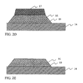
- FIGS. 2A–2E each shows a cross section of a substrate with a film, an oxide layer and a low contrast photoresist as processed following the methods according to the preferred teachings of the present invention to create a sharp structure with decontamination.
- FIGS. 3A–3E each shows a cross section of a substrate with a film, an oxide layer and low contrast photoresist as processed following the methods according to the preferred teachings of the present invention to create a sharp structure and a sharp structure on a film.
- FIGS. 4A–4F each shows a cross section of a substrate with a film, low contrast photoresist with an oxide layer having a sharp structure as processed following the methods according to the preferred teachings of the present invention.
- FIG. 5 shows a reticle having a triangular shape with a tip according to the preferred teachings of the present invention.
- FIG. 6A shows a low contrast photoresist pattern according to the preferred teachings of the present invention.
- FIG. 6B shows an oxide layer and low contrast photoresist after etch.
- FIG. 7 shows a process flow diagram of methods according to the preferred teachings of the present invention to form sharp corners and pointed features on a structure.
- FIG. 8 shows a process flow diagram of methods according to the preferred teachings of the present invention to form sharp corners and pointed features on a structure with decontamination.
- FIG. 9 shows a process flow diagram of methods according to the preferred teachings of the present invention to form sharp corners and pointed features on a structure and a film.
- FIG. 10 shows a process flow diagram of methods according to the preferred teachings of the present invention to form sharp corners and pointed features on a structure and a film that includes a decontamination procedure.
- the substrate 14 can be a semiconductor substrate, such as a silicon semiconductor substrate, and is suitable for the creation of semiconductor devices and electronic circuits.
- a semiconductor substrate such as a silicon semiconductor substrate
- any other material that is compatible with the methods of the present invention may be used to construct the substrate 14 and will be within the spirit and scope of the present invention.
- underlying circuitry is fabricated using conventional methods and processes, employing one or more layers of conventional interconnects to produce a partially connected and partially functional front-end.
- the upper layer of the front-end is a material of a thickness sufficient for the designed purpose of an electronic circuit. This front-end is then used as the substrate 14 on which the specialized circuitry is fabricated.
- FIGS. 1A–1D show a cross section of a structure with a sharp pointed structure 19 in an oxide layer 16 .
- the sharp pointed structure 19 can be an element of a bit structure 29 shown in FIG. 6B .
- Methods to construct pointed ends on a structure where the size of the pointed ends is near the limit of resolution of an optical exposure system start by providing the substrate 14 as diagrammatically illustrated by a box 20 in FIG. 7 .
- the oxide layer 16 is deposited on the substrate 14 using techniques well known in the art as diagrammatically illustrated by box 30 .
- the oxide layer 16 can be a silicon dioxide layer.
- the oxide layer 16 can be a silicon nitride layer.
- any other material that is compatible with the methods of the present invention may be used to construct the oxide layer 16 and will be within the spirit and scope of the present invention.
- a nitric oxide layer may be deposited on the substrate layer instead of the example silicon dioxide layer.
- the low contrast photoresist 17 can be a standard low contrast photoresist.
- any other material, compatible with the methods of the present invention, may be used to construct the low contrast photoresist 17 and will be within the spirit and scope of the present invention.
- the combination of the low contrast photoresist 17 with an etch process that is highly selective to the material being etched enables the creation of the sharp pointed structure 19 that, according to the preferred teachings of the present invention, is a sharp corner.
- the low contrast photoresist 17 is exposed to optical energy through a reticle 21 , creating the shape of the desired top cross section of the structure to be created, as diagrammatically illustrated by box 50 .
- the reticle 21 has a partially triangular shape 22 with a tip.
- the partially triangular shape 22 forms a partial equilateral triangle with a tip.
- the low contrast photoresist 17 is exposed to 90 millijoules of optical energy.
- the optical frequency corresponds to a G or I line stepper, in the blue light range, of approximately 90 millijoules, +/ ⁇ 5 millijoules for a 0.9 micron film.
- the layer of low contrast photoresist 17 is exposed to light of this frequency and for the appropriate duration to provide the correct amount of energy to the layer of low contrast photoresist 17 that, according to the preferred teachings of the present invention, is a low contrast photoresist film.
- the exposure time is a direct function of the optical frequency to deliver a prescribed amount of energy.
- the low contrast photoresist 17 is then developed to leave a foot 18 of the low contrast photoresist 17 in the area of the sharp pointed structure 19 as diagrammatically illustrated by box 60 .
- the low contrast photoresist 17 is developed using a developer that dissolves the weakly acidic exposed low contrast photoresist 17 .
- the oxide layer 16 is etched using an anisotropic etch process which etches the oxide layer 16 selectively to the low contrast photoresist 17 as diagrammatically illustrated by box 80 .
- an anisotropic etch process which etches the oxide layer 16 selectively to the low contrast photoresist 17 as diagrammatically illustrated by box 80 .
- slight erosion of the foot 18 causes the sharp pointed structure 19 at the end to become more pointed.
- the methods of the present invention significantly improves the transfer of a pointed shape or sharp corners from the low contrast photoresist 17 to a structure, the oxide layer 16 , whose dimensions are near the limit of an optical exposure system.
- FIGS. 2A–2E show a cross section of a structure with the sharp pointed structure 19 in the oxide layer 16 where a decontamination procedure has removed photoresist residue 27 .
- Methods to construct pointed ends on a structure where the size of the pointed ends is near the limit of resolution of an optical exposure system with a decontamination procedure start by providing the substrate 14 as diagrammatically illustrated by box 20 in FIG. 8 .
- Methods of FIG. 8 generally proceed as the methods of FIG. 7 with the addition of a decontamination procedure.
- An oxide layer 16 is deposited as diagrammatically shown in box 30 .
- the low contrast photoresist 17 is deposited on the oxide layer 16 as diagrammatically shown in box 40 .
- the low contrast photoresist 17 is exposed to optical energy as diagrammatically shown in box 50 .
- the low contrast photoresist 17 is developed as diagrammatically shown in box 60 .
- the developed low contrast photoresist 17 is decontaminated to remove any photoresist residue 27 that may remain as diagrammatically illustrated by box 70 .
- oxygen is introduced into the plasma to perform the decontamination procedure, also known as the descum procedure as is well known in the art.
- the low contrast photoresist 17 may be cured by heating it to an appropriate temperature to strengthen polymeric bonding in the low contrast photoresist 17 .
- wafers showed a small amount of photoresist residue 27 .
- the wafers with 10% overetch and no descum procedure show some amount of photoresist residue 27 .
- the other wafers do not have photoresist residue 27 except possibly at the 80 mJ/cm 2 dose. Wafers exposed at 80 mJ/cm 2 all have bridging. Wafers exposed at 90 mJ/cm 2 have pointed structures and have some rough edges in some cases. Wafers exposed at 100 and 110 mJ/cm 2 do not have very pointed structures. The best-looking result from experiment was the one with a descum procedure and a 10% overetch exposed at 90 mJ/cm 2 .
- Table A summaries results of decontamination on Critical Dimensions, CD, that are either a bit structure width or a bit structure length for the bit structure 29 .
- ⁇ Length is the change in length of the CD
- ⁇ Width is the change in width of the CD.
- FIGS. 3A–3E show a cross section of a structure with the sharp pointed structure 19 in the oxide layer 16 and a sharp pointed film structure 23 in a film 15 forming the bit structure 29 as shown in FIG. 6B .
- Methods to construct pointed ends on a structure and a film where the size of the pointed ends is near the limit of resolution of an optical exposure system with a decontamination procedure start by providing the substrate 14 as diagrammatically illustrated by box 20 in FIG. 9 .
- Methods of FIG. 9 generally proceed as the methods of FIG. 7 with the addition of the film 15 between the substrate 14 and the oxide layer 16 .
- the film 15 On top of the substrate 14 is deposited the film 15 of material that is constructed using techniques well known in the art as diagrammatically illustrated by box 25 .
- the film 15 is a metal film such as a 100 angstrom metal film made from a magnetoresistive material, also known as a magnetoresistive metal film.
- the film 15 can be aluminum, gold, or any other compatible metal.
- any other material that is compatible with the methods of the present invention may be used to construct the film 15 and will be within the spirit and scope of the present invention.
- Magnetoresistive random access memory elements rely on layers of magnetic film to store information.
- the shape of this structure is critical in the performance of this type of device.
- a structure with pointed ends results in better switching characteristics compared to a structure with flat ends. This is because the pointed end can prevent trapping magnetic domains in the device, which may alter the switch thresholds and signal strength of the device.
- the processes are useful for the fabrication of a variety of active and passive circuit elements. These generic circuit elements are referred to as metal structures, which include, but are not limited to, a variety of magnetic devices.
- the oxide layer 16 is deposited as diagrammatically shown in box 30 .
- the low contrast photoresist 17 is deposited on the oxide layer 16 as diagrammatically shown in box 40 .
- the low contrast photoresist 17 is exposed to optical energy as diagrammatically shown in box 50 .
- the low contrast photoresist 17 is developed as diagrammatically shown in box 60 .
- the oxide layer 16 is etched using an anisotropic etch process which etches the oxide layer 16 selectively to the low contrast photoresist 17 as diagrammatically illustrated by box 80 .
- an anisotropic etch process which etches the oxide layer 16 selectively to the low contrast photoresist 17 as diagrammatically illustrated by box 80 .
- the methods of the present invention significantly improves the transfer of a pointed shape or sharp corners from the low contrast photoresist 17 to a structure whose dimensions are near the limit of an optical exposure system.
- CD's were measured at five sites on a wafer processed with the methods of the present invention. The negative CD change indicates that the CD's were larger after etch.
- the foot 18 When low contrast photoresist 17 is exposed near the limit of its exposure dose, the foot 18 can be formed at the pointed tip of the structure following the preferred teachings of the present invention.
- the foot 18 plays a critical role in the creation of the bit structure 29 .
- the photoresist residue 27 was mostly affected by the UV cure vs. hardbake parameter. There is some photoresist residue 27 in the field at the bit ends.
- Wafer experiment# 5 has the best overall process from this set except for the photoresist residue 27 on the bits.
- Wafer experiment# 7 has the least photoresist residue 27 on the bit hardmask oxide.
- the low contrast photoresist 17 is removed in a well-known manner as is diagrammatically shown in box 90 . This exposes the oxide layer 16 to further processing.
- the film 15 is then etched to form the sharp pointed film structure 23 as is diagrammatically shown in box 100 .
- FIGS. 4A–4F show a cross section of a structure with the sharp pointed structure 19 in the oxide layer 16 and the sharp pointed film structure 23 in the film 15 where a decontamination procedure has removed photoresist residue 27 .
- Methods to construct pointed ends on a structure and the film 15 where the size of the sharp pointed film structure 23 is near the limit of resolution of an optical exposure system start by providing the substrate 14 as diagrammatically illustrated by box 20 in FIG. 10 .
- the film 15 of material that is constructed using techniques well known in the art as diagrammatically illustrated by box 25 .
- the oxide layer 16 is deposited on the film 15 using techniques well know in the art as diagrammatically illustrated by box 30 .
- the low contrast photoresist 17 is deposited using techniques well know in the art as diagrammatically illustrated by box 40 .
- the combination of the low contrast photoresist 17 with an etch process which is highly selective to the material being etched, the oxide layer 16 , over low contrast photoresist 17 enables the creation of the sharp pointed structure 19 as a sharp corner.
- the low contrast photoresist 17 is exposed to optical energy through a reticle 21 , with the photomask creating the shape of the desired top cross section of the structure to be created, as diagrammatically illustrated by box 50 .
- the low contrast photoresist 17 is then developed to leave the foot 18 of low contrast photoresist 17 in the area of the sharp pointed structure 19 at the end as diagrammatically illustrated by box 60 .
- the developed low contrast photoresist 17 is then decontaminated to remove any photoresist residue 27 that may remain as diagrammatically illustrated by box 70 .
- the oxide layer 16 is etched using an anisotropic etch process which etches the oxide layer 16 selectively to the low contrast photoresist 17 as diagrammatically illustrated by box 80 .
- the low contrast photoresist 17 is removed in a well-known manner as is diagrammatically shown in box 90 . This exposes the oxide layer 16 to further processing.
- the film 15 is then etched to form the sharp pointed film structure 23 as is diagrammatically shown in box 100 .
Abstract
Description
| TABLE A | ||||||
| Dose | ||||||
| (milli | Bit Length | Bit Width | ||||
| Wafer | Site | Joules) | Descum | Overetch | (microns) | (microns) |
| 2 | 5 | 110 | 0 | 10% | 2.44 | .66 |
| 6 | 100 | 0 | 10% | 2.68 | .68 | |
| 7 | 90 | 0 | 10% | 3.11 | .72 | |
| 3 | 5 | 110 | 500 | 10% | 2.28 | .53 |
| 6 | 100 | 500 | 10% | 2.35 | .59 | |
| 7 | 90 | 500 | 10% | 2.72 | .60 | |
| 4 | 5 | 110 | 0 | 40% | 2.35 | .59 |
| 6 | 100 | 0 | 40% | 2.59 | .62 | |
| 7 | 90 | 0 | 40% | 3.17 | .70 | |
| 6 | 5 | 110 | 500 | 40% | 2.23 | .52 |
| 6 | 100 | 500 | 40% | 2.37 | .54 | |
| 7 | 90 | 500 | 40% | 2.56 | .46 | |
| Effect | Dose | ΔLength | ΔWidth | |||
| Overetch | 110 | .07 | .04 | |||
| 100 | .04 | .05 | ||||
| 90 | .05 | .09 | ||||
| Descum | 110 | .14 | .10 | |||
| 100 | .28 | .09 | ||||
| 90 | .50 | .18 | ||||
| TABLE B | ||||||||
| Avg | Avg | Std | CD | |||||
| Se- | Norm* | Norm* | Dev | Change | ||||
| UV | lec- | CD | CD | Bits | Bits | |||
| Exp # | Resist | Cure | tivity | OE | Bit 2 | Bit 6 | 2 & 6 | 2 & 6 |
| 1 | 7908 | UV | 7:1 | 20 | 2.598 | 3.702 | .0883 | −.118 |
| .0601 | −.102 | |||||||
| 2 | 7908 | UV | 15:1 | 40 | 2.642 | 3.720 | .0767 | −.122 |
| .0828 | −.100 | |||||||
| 3 | 7908 | HB | 7:1 | 40 | 2.626 | 3.645 | .0471 | −.106 |
| .0880 | .015 | |||||||
| 4 | 7908 | HB | 15:1 | 20 | 2.760 | 3.893 | .0659 | −.240 |
| .1038 | −.243 | |||||||
| 5 | 3312 | UV | 7:1 | 40 | 2.473 | 3.552 | .0666 | −.073 |
| .0561 | −.052 | |||||||
| 6 | 3312 | UV | 15:1 | 20 | 2.481 | 3.696 | .0794 | −.051 |
| .1562 | −.256 | |||||||
| 7 | 3312 | HB | 7:1 | 20 | 2.667 | 3.659 | .0630 | −.227 |
| .0899 | −.149 | |||||||
| *Normalized to the pitch of the device. | ||||||||
Claims (20)
Priority Applications (1)
| Application Number | Priority Date | Filing Date | Title |
|---|---|---|---|
| US10/397,614 US7022247B2 (en) | 2003-03-26 | 2003-03-26 | Process to form fine features using photolithography and plasma etching |
Applications Claiming Priority (1)
| Application Number | Priority Date | Filing Date | Title |
|---|---|---|---|
| US10/397,614 US7022247B2 (en) | 2003-03-26 | 2003-03-26 | Process to form fine features using photolithography and plasma etching |
Publications (2)
| Publication Number | Publication Date |
|---|---|
| US20040188382A1 US20040188382A1 (en) | 2004-09-30 |
| US7022247B2 true US7022247B2 (en) | 2006-04-04 |
Family
ID=32989038
Family Applications (1)
| Application Number | Title | Priority Date | Filing Date |
|---|---|---|---|
| US10/397,614 Expired - Fee Related US7022247B2 (en) | 2003-03-26 | 2003-03-26 | Process to form fine features using photolithography and plasma etching |
Country Status (1)
| Country | Link |
|---|---|
| US (1) | US7022247B2 (en) |
Families Citing this family (3)
| Publication number | Priority date | Publication date | Assignee | Title |
|---|---|---|---|---|
| US7183042B2 (en) * | 2003-11-12 | 2007-02-27 | Honeywell International Inc. | Bit end design for pseudo spin valve (PSV) devices |
| JP5543873B2 (en) * | 2010-07-30 | 2014-07-09 | Hoya株式会社 | REFLECTIVE MASK BLANK, MANUFACTURING METHOD THEREOF, AND REFLECTIVE MASK |
| CN114137792A (en) * | 2021-10-29 | 2022-03-04 | 中国科学院微电子研究所 | Mask parameter optimization method and device |
Citations (10)
| Publication number | Priority date | Publication date | Assignee | Title |
|---|---|---|---|---|
| US5320981A (en) * | 1993-08-10 | 1994-06-14 | Micron Semiconductor, Inc. | High accuracy via formation for semiconductor devices |
| US5790512A (en) | 1993-12-24 | 1998-08-04 | U.S. Philips Corporation | Optical information carrier |
| US6190989B1 (en) * | 1998-07-15 | 2001-02-20 | Micron Technology, Inc. | Method for patterning cavities and enhanced cavity shapes for semiconductor devices |
| US20010016385A1 (en) * | 1999-05-03 | 2001-08-23 | Taiwan Semiconductor Manufacturing Company | Novel process for preventing the reverse tunneling during programming in split gate flash |
| US6333456B1 (en) * | 1998-01-22 | 2001-12-25 | Citizen Watch Co., Ltd. | Solar cell device and method of producing the same |
| US6417108B1 (en) * | 1998-02-04 | 2002-07-09 | Canon Kabushiki Kaisha | Semiconductor substrate and method of manufacturing the same |
| US20020089787A1 (en) * | 2001-01-10 | 2002-07-11 | Jennifer Lu | Method for producing a transducer slider with tapered edges |
| US6475884B2 (en) * | 2000-07-17 | 2002-11-05 | General Semiconductor, Inc. | Devices and methods for addressing optical edge effects in connection with etched trenches |
| US6566269B1 (en) * | 2000-07-14 | 2003-05-20 | Lucent Technologies Inc. | Removal of post etch residuals on wafer surface |
| US6783994B2 (en) * | 2002-04-26 | 2004-08-31 | Freescale Semiconductor, Inc. | Method of fabricating a self-aligned magnetic tunneling junction and via contact |
-
2003
- 2003-03-26 US US10/397,614 patent/US7022247B2/en not_active Expired - Fee Related
Patent Citations (10)
| Publication number | Priority date | Publication date | Assignee | Title |
|---|---|---|---|---|
| US5320981A (en) * | 1993-08-10 | 1994-06-14 | Micron Semiconductor, Inc. | High accuracy via formation for semiconductor devices |
| US5790512A (en) | 1993-12-24 | 1998-08-04 | U.S. Philips Corporation | Optical information carrier |
| US6333456B1 (en) * | 1998-01-22 | 2001-12-25 | Citizen Watch Co., Ltd. | Solar cell device and method of producing the same |
| US6417108B1 (en) * | 1998-02-04 | 2002-07-09 | Canon Kabushiki Kaisha | Semiconductor substrate and method of manufacturing the same |
| US6190989B1 (en) * | 1998-07-15 | 2001-02-20 | Micron Technology, Inc. | Method for patterning cavities and enhanced cavity shapes for semiconductor devices |
| US20010016385A1 (en) * | 1999-05-03 | 2001-08-23 | Taiwan Semiconductor Manufacturing Company | Novel process for preventing the reverse tunneling during programming in split gate flash |
| US6566269B1 (en) * | 2000-07-14 | 2003-05-20 | Lucent Technologies Inc. | Removal of post etch residuals on wafer surface |
| US6475884B2 (en) * | 2000-07-17 | 2002-11-05 | General Semiconductor, Inc. | Devices and methods for addressing optical edge effects in connection with etched trenches |
| US20020089787A1 (en) * | 2001-01-10 | 2002-07-11 | Jennifer Lu | Method for producing a transducer slider with tapered edges |
| US6783994B2 (en) * | 2002-04-26 | 2004-08-31 | Freescale Semiconductor, Inc. | Method of fabricating a self-aligned magnetic tunneling junction and via contact |
Also Published As
| Publication number | Publication date |
|---|---|
| US20040188382A1 (en) | 2004-09-30 |
Similar Documents
| Publication | Publication Date | Title |
|---|---|---|
| US6383952B1 (en) | RELACS process to double the frequency or pitch of small feature formation | |
| TW535209B (en) | Method of forming fine patterns in semiconductor device | |
| US4098917A (en) | Method of providing a patterned metal layer on a substrate employing metal mask and ion milling | |
| JP3218814B2 (en) | Method for manufacturing semiconductor device | |
| US3957552A (en) | Method for making multilayer devices using only a single critical masking step | |
| JP2004179254A (en) | Method for manufacturing semiconductor device | |
| US6664026B2 (en) | Method of manufacturing high aspect ratio photolithographic features | |
| KR20170122161A (en) | Magnetic core, inductor, and method for fabricating the magnetic core | |
| US6774044B2 (en) | Reducing photoresist shrinkage via plasma treatment | |
| US4487795A (en) | Method of forming patterned conductor lines | |
| US7022247B2 (en) | Process to form fine features using photolithography and plasma etching | |
| EP0940719A2 (en) | Photoresist film and method for forming a pattern thereof | |
| US6090523A (en) | Multi-resin material for an antireflection film to be formed on a workpiece disposed on a semiconductor substrate | |
| JP3210705B2 (en) | Phase shift photomask | |
| US6316166B1 (en) | Method of forming micro pattern of semiconductor device | |
| JP3222531B2 (en) | Method for manufacturing photomask having phase shift layer | |
| EP0104235A4 (en) | Electron beam-optical hybrid lithographic resist process. | |
| KR100376882B1 (en) | Method for forming fine pattern of semiconductor device | |
| JPH07106327A (en) | Semiconductor device and its manufacture | |
| KR19980050146A (en) | Method of forming fine pattern of semiconductor device | |
| JPH02192714A (en) | Formation of resist pattern | |
| KR940009996B1 (en) | Manufacturing method of semiconductor device | |
| JPH0738386B2 (en) | Etching method | |
| KR20060023338A (en) | Lithography mask of semiconductor device and method using the same | |
| TW461041B (en) | Forming method of borderless contact |
Legal Events
| Date | Code | Title | Description |
|---|---|---|---|
| AS | Assignment |
Owner name: RIDER BENNETT, LLP, MINNESOTA Free format text: ATTORNEY'S LIEN RELEASE;ASSIGNOR:UNION SEMICONDUCTOR TECHNOLOGY CORPORATION;REEL/FRAME:014149/0364 Effective date: 20031031 |
|
| AS | Assignment |
Owner name: UNION SEMICONDUCTOR TECHNOLOGY CORPORATION, MINNES Free format text: ASSIGNMENT OF ASSIGNORS INTEREST;ASSIGNOR:MIKELSON, HANS PETER;REEL/FRAME:015790/0038 Effective date: 20040823 |
|
| AS | Assignment |
Owner name: UNION SEMICONDUCTOR TECHNOLOGY CORPORATION, MINNES Free format text: ASSIGNMENT OF ASSIGNORS INTEREST;ASSIGNOR:LOBOS, GEORGE JAMES;REEL/FRAME:016031/0712 Effective date: 20041015 |
|
| AS | Assignment |
Owner name: RIDER BENNETT, LLP, MINNESOTA Free format text: ATTORNEY'S LIEN;ASSIGNOR:UNION SEMICONDUCTOR TECHNOLOGY CORPORATION;REEL/FRAME:017186/0335 Effective date: 20050329 |
|
| AS | Assignment |
Owner name: RIDER BENNETT, LLP, MINNESOTA Free format text: ATTORNEY'S LIEN;ASSIGNOR:UNION SEMICONDUCTOR TECHNOLOGY CORPORATION;REEL/FRAME:017136/0929 Effective date: 20050329 |
|
| CC | Certificate of correction | ||
| FPAY | Fee payment |
Year of fee payment: 4 |
|
| FPAY | Fee payment |
Year of fee payment: 8 |
|
| FEPP | Fee payment procedure |
Free format text: MAINTENANCE FEE REMINDER MAILED (ORIGINAL EVENT CODE: REM.) |
|
| LAPS | Lapse for failure to pay maintenance fees |
Free format text: PATENT EXPIRED FOR FAILURE TO PAY MAINTENANCE FEES (ORIGINAL EVENT CODE: EXP.) |
|
| STCH | Information on status: patent discontinuation |
Free format text: PATENT EXPIRED DUE TO NONPAYMENT OF MAINTENANCE FEES UNDER 37 CFR 1.362 |
|
| FP | Lapsed due to failure to pay maintenance fee |
Effective date: 20180404 |