US7023046B2 - Undoped oxide liner/BPSG for improved data retention - Google Patents
Undoped oxide liner/BPSG for improved data retention Download PDFInfo
- Publication number
- US7023046B2 US7023046B2 US10/617,450 US61745003A US7023046B2 US 7023046 B2 US7023046 B2 US 7023046B2 US 61745003 A US61745003 A US 61745003A US 7023046 B2 US7023046 B2 US 7023046B2
- Authority
- US
- United States
- Prior art keywords
- oxide
- undoped
- oxide liner
- present
- data retention
- Prior art date
- Legal status (The legal status is an assumption and is not a legal conclusion. Google has not performed a legal analysis and makes no representation as to the accuracy of the status listed.)
- Expired - Lifetime, expires
Links
- 239000005380 borophosphosilicate glass Substances 0.000 title claims abstract description 12
- 230000014759 maintenance of location Effects 0.000 title abstract description 17
- 239000004065 semiconductor Substances 0.000 claims abstract description 23
- 229910052814 silicon oxide Inorganic materials 0.000 claims abstract description 19
- VYPSYNLAJGMNEJ-UHFFFAOYSA-N Silicium dioxide Chemical compound O=[Si]=O VYPSYNLAJGMNEJ-UHFFFAOYSA-N 0.000 claims abstract description 17
- BOTDANWDWHJENH-UHFFFAOYSA-N Tetraethyl orthosilicate Chemical compound CCO[Si](OCC)(OCC)OCC BOTDANWDWHJENH-UHFFFAOYSA-N 0.000 claims abstract description 8
- 239000000758 substrate Substances 0.000 claims description 7
- 229910052796 boron Inorganic materials 0.000 claims description 4
- ZOXJGFHDIHLPTG-UHFFFAOYSA-N Boron Chemical compound [B] ZOXJGFHDIHLPTG-UHFFFAOYSA-N 0.000 claims description 3
- BHEPBYXIRTUNPN-UHFFFAOYSA-N hydridophosphorus(.) (triplet) Chemical compound [PH] BHEPBYXIRTUNPN-UHFFFAOYSA-N 0.000 claims description 3
- 150000004767 nitrides Chemical class 0.000 claims description 2
- 239000000126 substance Substances 0.000 claims 1
- 238000000151 deposition Methods 0.000 abstract description 24
- 230000008021 deposition Effects 0.000 abstract description 14
- 238000011065 in-situ storage Methods 0.000 abstract description 5
- 238000005229 chemical vapour deposition Methods 0.000 abstract description 2
- 238000004519 manufacturing process Methods 0.000 description 17
- 239000010410 layer Substances 0.000 description 14
- 229910052581 Si3N4 Inorganic materials 0.000 description 5
- 238000000034 method Methods 0.000 description 5
- HQVNEWCFYHHQES-UHFFFAOYSA-N silicon nitride Chemical compound N12[Si]34N5[Si]62N3[Si]51N64 HQVNEWCFYHHQES-UHFFFAOYSA-N 0.000 description 5
- FVBUAEGBCNSCDD-UHFFFAOYSA-N silicide(4-) Chemical compound [Si-4] FVBUAEGBCNSCDD-UHFFFAOYSA-N 0.000 description 4
- 238000012986 modification Methods 0.000 description 3
- 230000004048 modification Effects 0.000 description 3
- 238000004151 rapid thermal annealing Methods 0.000 description 3
- 125000006850 spacer group Chemical group 0.000 description 3
- AJSTXXYNEIHPMD-UHFFFAOYSA-N triethyl borate Chemical compound CCOB(OCC)OCC AJSTXXYNEIHPMD-UHFFFAOYSA-N 0.000 description 3
- 230000007547 defect Effects 0.000 description 2
- 230000001747 exhibiting effect Effects 0.000 description 2
- 239000001257 hydrogen Substances 0.000 description 2
- 229910052739 hydrogen Inorganic materials 0.000 description 2
- 239000011229 interlayer Substances 0.000 description 2
- 239000002184 metal Substances 0.000 description 2
- 229910021332 silicide Inorganic materials 0.000 description 2
- CBENFWSGALASAD-UHFFFAOYSA-N Ozone Chemical compound [O-][O+]=O CBENFWSGALASAD-UHFFFAOYSA-N 0.000 description 1
- XUIMIQQOPSSXEZ-UHFFFAOYSA-N Silicon Chemical compound [Si] XUIMIQQOPSSXEZ-UHFFFAOYSA-N 0.000 description 1
- 230000015572 biosynthetic process Effects 0.000 description 1
- 230000001934 delay Effects 0.000 description 1
- 238000013461 design Methods 0.000 description 1
- 239000002019 doping agent Substances 0.000 description 1
- 230000009977 dual effect Effects 0.000 description 1
- 238000005530 etching Methods 0.000 description 1
- 239000007789 gas Substances 0.000 description 1
- 239000001307 helium Substances 0.000 description 1
- 229910052734 helium Inorganic materials 0.000 description 1
- SWQJXJOGLNCZEY-UHFFFAOYSA-N helium atom Chemical compound [He] SWQJXJOGLNCZEY-UHFFFAOYSA-N 0.000 description 1
- 150000002431 hydrogen Chemical class 0.000 description 1
- -1 hydrogen ions Chemical class 0.000 description 1
- 238000011835 investigation Methods 0.000 description 1
- 229910021421 monocrystalline silicon Inorganic materials 0.000 description 1
- 238000012545 processing Methods 0.000 description 1
- 229910052710 silicon Inorganic materials 0.000 description 1
- 239000010703 silicon Substances 0.000 description 1
- 239000011800 void material Substances 0.000 description 1
Images

Classifications
-
- H—ELECTRICITY
- H01—ELECTRIC ELEMENTS
- H01L—SEMICONDUCTOR DEVICES NOT COVERED BY CLASS H10
- H01L21/00—Processes or apparatus adapted for the manufacture or treatment of semiconductor or solid state devices or of parts thereof
- H01L21/02—Manufacture or treatment of semiconductor devices or of parts thereof
- H01L21/02104—Forming layers
- H01L21/02107—Forming insulating materials on a substrate
- H01L21/02109—Forming insulating materials on a substrate characterised by the type of layer, e.g. type of material, porous/non-porous, pre-cursors, mixtures or laminates
- H01L21/02112—Forming insulating materials on a substrate characterised by the type of layer, e.g. type of material, porous/non-porous, pre-cursors, mixtures or laminates characterised by the material of the layer
- H01L21/02123—Forming insulating materials on a substrate characterised by the type of layer, e.g. type of material, porous/non-porous, pre-cursors, mixtures or laminates characterised by the material of the layer the material containing silicon
- H01L21/02126—Forming insulating materials on a substrate characterised by the type of layer, e.g. type of material, porous/non-porous, pre-cursors, mixtures or laminates characterised by the material of the layer the material containing silicon the material containing Si, O, and at least one of H, N, C, F, or other non-metal elements, e.g. SiOC, SiOC:H or SiONC
- H01L21/02129—Forming insulating materials on a substrate characterised by the type of layer, e.g. type of material, porous/non-porous, pre-cursors, mixtures or laminates characterised by the material of the layer the material containing silicon the material containing Si, O, and at least one of H, N, C, F, or other non-metal elements, e.g. SiOC, SiOC:H or SiONC the material being boron or phosphorus doped silicon oxides, e.g. BPSG, BSG or PSG
-
- H—ELECTRICITY
- H01—ELECTRIC ELEMENTS
- H01L—SEMICONDUCTOR DEVICES NOT COVERED BY CLASS H10
- H01L21/00—Processes or apparatus adapted for the manufacture or treatment of semiconductor or solid state devices or of parts thereof
- H01L21/02—Manufacture or treatment of semiconductor devices or of parts thereof
- H01L21/02104—Forming layers
- H01L21/02107—Forming insulating materials on a substrate
- H01L21/02109—Forming insulating materials on a substrate characterised by the type of layer, e.g. type of material, porous/non-porous, pre-cursors, mixtures or laminates
- H01L21/02112—Forming insulating materials on a substrate characterised by the type of layer, e.g. type of material, porous/non-porous, pre-cursors, mixtures or laminates characterised by the material of the layer
- H01L21/02123—Forming insulating materials on a substrate characterised by the type of layer, e.g. type of material, porous/non-porous, pre-cursors, mixtures or laminates characterised by the material of the layer the material containing silicon
- H01L21/02164—Forming insulating materials on a substrate characterised by the type of layer, e.g. type of material, porous/non-porous, pre-cursors, mixtures or laminates characterised by the material of the layer the material containing silicon the material being a silicon oxide, e.g. SiO2
-
- H—ELECTRICITY
- H01—ELECTRIC ELEMENTS
- H01L—SEMICONDUCTOR DEVICES NOT COVERED BY CLASS H10
- H01L21/00—Processes or apparatus adapted for the manufacture or treatment of semiconductor or solid state devices or of parts thereof
- H01L21/02—Manufacture or treatment of semiconductor devices or of parts thereof
- H01L21/02104—Forming layers
- H01L21/02107—Forming insulating materials on a substrate
- H01L21/02109—Forming insulating materials on a substrate characterised by the type of layer, e.g. type of material, porous/non-porous, pre-cursors, mixtures or laminates
- H01L21/022—Forming insulating materials on a substrate characterised by the type of layer, e.g. type of material, porous/non-porous, pre-cursors, mixtures or laminates the layer being a laminate, i.e. composed of sublayers, e.g. stacks of alternating high-k metal oxides
-
- H—ELECTRICITY
- H01—ELECTRIC ELEMENTS
- H01L—SEMICONDUCTOR DEVICES NOT COVERED BY CLASS H10
- H01L21/00—Processes or apparatus adapted for the manufacture or treatment of semiconductor or solid state devices or of parts thereof
- H01L21/02—Manufacture or treatment of semiconductor devices or of parts thereof
- H01L21/02104—Forming layers
- H01L21/02107—Forming insulating materials on a substrate
- H01L21/02225—Forming insulating materials on a substrate characterised by the process for the formation of the insulating layer
- H01L21/0226—Forming insulating materials on a substrate characterised by the process for the formation of the insulating layer formation by a deposition process
- H01L21/02263—Forming insulating materials on a substrate characterised by the process for the formation of the insulating layer formation by a deposition process deposition from the gas or vapour phase
- H01L21/02271—Forming insulating materials on a substrate characterised by the process for the formation of the insulating layer formation by a deposition process deposition from the gas or vapour phase deposition by decomposition or reaction of gaseous or vapour phase compounds, i.e. chemical vapour deposition
-
- H—ELECTRICITY
- H01—ELECTRIC ELEMENTS
- H01L—SEMICONDUCTOR DEVICES NOT COVERED BY CLASS H10
- H01L21/00—Processes or apparatus adapted for the manufacture or treatment of semiconductor or solid state devices or of parts thereof
- H01L21/02—Manufacture or treatment of semiconductor devices or of parts thereof
- H01L21/04—Manufacture or treatment of semiconductor devices or of parts thereof the devices having at least one potential-jump barrier or surface barrier, e.g. PN junction, depletion layer or carrier concentration layer
- H01L21/18—Manufacture or treatment of semiconductor devices or of parts thereof the devices having at least one potential-jump barrier or surface barrier, e.g. PN junction, depletion layer or carrier concentration layer the devices having semiconductor bodies comprising elements of Group IV of the Periodic System or AIIIBV compounds with or without impurities, e.g. doping materials
- H01L21/30—Treatment of semiconductor bodies using processes or apparatus not provided for in groups H01L21/20 - H01L21/26
- H01L21/31—Treatment of semiconductor bodies using processes or apparatus not provided for in groups H01L21/20 - H01L21/26 to form insulating layers thereon, e.g. for masking or by using photolithographic techniques; After treatment of these layers; Selection of materials for these layers
- H01L21/314—Inorganic layers
- H01L21/316—Inorganic layers composed of oxides or glassy oxides or oxide based glass
- H01L21/31604—Deposition from a gas or vapour
- H01L21/31625—Deposition of boron or phosphorus doped silicon oxide, e.g. BSG, PSG, BPSG
-
- H—ELECTRICITY
- H01—ELECTRIC ELEMENTS
- H01L—SEMICONDUCTOR DEVICES NOT COVERED BY CLASS H10
- H01L29/00—Semiconductor devices adapted for rectifying, amplifying, oscillating or switching, or capacitors or resistors with at least one potential-jump barrier or surface barrier, e.g. PN junction depletion layer or carrier concentration layer; Details of semiconductor bodies or of electrodes thereof ; Multistep manufacturing processes therefor
- H01L29/40—Electrodes ; Multistep manufacturing processes therefor
- H01L29/43—Electrodes ; Multistep manufacturing processes therefor characterised by the materials of which they are formed
- H01L29/49—Metal-insulator-semiconductor electrodes, e.g. gates of MOSFET
- H01L29/51—Insulating materials associated therewith
- H01L29/511—Insulating materials associated therewith with a compositional variation, e.g. multilayer structures
-
- H—ELECTRICITY
- H10—SEMICONDUCTOR DEVICES; ELECTRIC SOLID-STATE DEVICES NOT OTHERWISE PROVIDED FOR
- H10B—ELECTRONIC MEMORY DEVICES
- H10B41/00—Electrically erasable-and-programmable ROM [EEPROM] devices comprising floating gates
- H10B41/30—Electrically erasable-and-programmable ROM [EEPROM] devices comprising floating gates characterised by the memory core region
-
- H—ELECTRICITY
- H10—SEMICONDUCTOR DEVICES; ELECTRIC SOLID-STATE DEVICES NOT OTHERWISE PROVIDED FOR
- H10B—ELECTRONIC MEMORY DEVICES
- H10B69/00—Erasable-and-programmable ROM [EPROM] devices not provided for in groups H10B41/00 - H10B63/00, e.g. ultraviolet erasable-and-programmable ROM [UVEPROM] devices
-
- H—ELECTRICITY
- H01—ELECTRIC ELEMENTS
- H01L—SEMICONDUCTOR DEVICES NOT COVERED BY CLASS H10
- H01L21/00—Processes or apparatus adapted for the manufacture or treatment of semiconductor or solid state devices or of parts thereof
- H01L21/02—Manufacture or treatment of semiconductor devices or of parts thereof
- H01L21/04—Manufacture or treatment of semiconductor devices or of parts thereof the devices having at least one potential-jump barrier or surface barrier, e.g. PN junction, depletion layer or carrier concentration layer
- H01L21/18—Manufacture or treatment of semiconductor devices or of parts thereof the devices having at least one potential-jump barrier or surface barrier, e.g. PN junction, depletion layer or carrier concentration layer the devices having semiconductor bodies comprising elements of Group IV of the Periodic System or AIIIBV compounds with or without impurities, e.g. doping materials
- H01L21/30—Treatment of semiconductor bodies using processes or apparatus not provided for in groups H01L21/20 - H01L21/26
- H01L21/31—Treatment of semiconductor bodies using processes or apparatus not provided for in groups H01L21/20 - H01L21/26 to form insulating layers thereon, e.g. for masking or by using photolithographic techniques; After treatment of these layers; Selection of materials for these layers
- H01L21/314—Inorganic layers
- H01L21/316—Inorganic layers composed of oxides or glassy oxides or oxide based glass
- H01L21/31604—Deposition from a gas or vapour
- H01L21/31608—Deposition of SiO2
- H01L21/31612—Deposition of SiO2 on a silicon body
Definitions
- the present invention relates to a method of manufacturing semiconductor devices having high reliability and improved data retention.
- the present invention has particular applicability in manufacturing high density, multi-level flash memory devices with improved data retention and improved gap filling.
- non-volatile semiconductor devices such as flash memory devices, e.g., electrically erasable programmable read only memory (EEPROM) devices.
- flash memory devices comprising transistors having a gate width of about 0.13 micron and under and gate structures spaced apart by a small gap of about 0.30 micron or less.
- an oxide sidewall spacer is formed on side surfaces of the gate stack, thereby reducing the gap to about 0.125 micron, and a conformal silicon nitride layer deposited thereon.
- the first interlayer dielectric (ILDO) is then deposited over the gate structures filling the gaps therebetween. Rapid thermal annealing is then conducted, as at a temperature of about 820° C. for about 120 seconds.
- ILDO first interlayer dielectric
- An advantage of the present invention is a method of manufacturing flash memory semiconductor devices with improved data retention and improved reliability.
- Another advantage of the present invention is a flash memory semiconductor device having improved data retention and improved reliability.
- a method of manufacturing a semiconductor device comprising: forming two gate electrode structures, spaced apart by a gap, on a semiconductor substrate; depositing an undoped oxide liner on the gate electrode structures and into the gap; and depositing a layer of boron (B) and phosphorous (P)-doped silicon oxide (BPSG) on the undoped oxide liner filling the gap.
- B boron
- P phosphorous
- BPSG boron-doped silicon oxide
- Embodiments of the present invention include depositing an undoped silicon oxide liner derived from tetraethyl orthosilicate (TEOS) by sub-atmospheric-chemical vapor deposition (SA-CVD), as at a thickness of 400 ⁇ to 600 ⁇ , and thereafter depositing in-situ the BPSG layer by SA-CVD in the same deposition chamber under otherwise essentially the same deposition conditions by introducing triethylborate (TEB) and triethylphosophate (TEPO).
- TEB triethylborate
- TEPO triethylphosophate
- Another aspect of the present invention is a semiconductor device comprising: two gate electrode structures, spaced apart by a gap, on a semiconductor substrate; an undoped oxide liner on the gate electrode structures in the gap; and a layer of boron (B) and phosphorous (P)-doped silicon oxide (BPSG) on the undoped oxide liner filling the gap.
- Embodiments of the present invention include semiconductor devices with gate electrode structures comprising a tunnel oxide on the semiconductor substrate, a floating gate electrode on the tunnel oxide, an interpoly dielectric comprising an oxide/nitride/oxide (ONO) stack on the floating gate; and a control gate electrode on the interpoly dielectrode.
- Embodiments of the present invention further include gate electrode structures with silicon oxide sidewall spacers on side surfaces thereof.
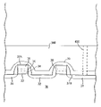
- FIG. 1 schematically illustrates an embodiment of the present invention.
- the present invention addresses and solves various reliability problems which arise in fabricating microminiaturized semiconductor devices, such as flash memory devices, e.g., data retention and gap filling.
- the present invention provides efficient methodology enabling the fabrication of semiconductor devices exhibiting greater reliability and improved data retention.
- the present invention addressees and solves such data retention problems by strategically removing the conventional silicon nitride liner and replacing it with an undoped oxide liner prior to depositing the first interlayer dielectric (ILD 0 ).
- the undoped silicon oxide liner and subsequent ILD 0 are deposited in the same chamber, in-situ, under basically the same deposition conditions except that dopant sources are introduced during deposition of the ILDO, such as B and P sources when depositing BPSG.
- dopant sources are introduced during deposition of the ILDO, such as B and P sources when depositing BPSG.
- This technique advantageously results in superior gap filled properties and reduces defects because of the reduction in wafer handling.
- cycle time is improved, thereby increasing manufacturing throughput.
- the undoped silicon oxide liner may be deposited by SA-CVD at a TEOS flow rate of 400 to 600 mgm, e.g., 500 mgm, and ozone (O 3 ) flow rate of 3,600 to 4,400 sccm, e.g., 4,000 sccm, a helium (He) flow rate of 5,400 to 6,600 sccm, e.g., 6,000 sccm, a pressure of 180 to 220 Torr, e.g., 200 Torr, a temperature of 460° C.
- TEOS flow rate 400 to 600 mgm, e.g., 500 mgm
- O 3 ozone
- He helium
- Deposition of the undoped silicon oxide liner may be implemented for about 30 seconds to 38 seconds, e.g., 34 seconds, to deposit the undoped silicon liner at a thickness of 400 ⁇ to 600 ⁇ , e.g., 500 ⁇ .
- SA-CVD deposition is continued under basically the same conditions except that TEB is introduced at a flow rate of 123 to 183 mgm, e.g., 153 mgm, and TEPO is introduced at a flow rate of 31 to 71 mgm, e.g., 51 mgm, while continuing introduction of TEOS at a flow rate of 400 to 600 mgm, e.g., 500 mgm, O 3 at a flow rate of 3,600 to 4,400 sccm, e.g., 4,000 sccm, He at a flow rate of 5,400 to 6,600 sccm, e.g., 6,000 sccm, and maintaining the pressure at 180 to 220 Torr, e.g., 200 Torr, temperature at 460° C.
- TEB is introduced at a flow rate of 123 to 183 mgm, e.g., 153 mgm
- TEPO is introduced at a flow rate of 31 to 71 mgm, e.g., 51 mg
- Deposition of the BPSG layer may be conducted for a period of time sufficient to obtain a desired thickness, such as 123 seconds to 151 seconds, e.g., 134 seconds, to provide a BPSG layer thickness of 11,000 ⁇ to 13,000 ⁇ , e.g., 12,000 ⁇ .
- rapid thermal annealing may be conducted as at a temperature 820° C. and for 120 seconds.
- FIG. 1 An embodiment of the present invention is schematically illustrated in FIG. 1 wherein transistors are formed on substrate 30 .
- Substrate 30 may comprise doped monocrystalline silicon or a plurality of wells or epitxial layers.
- the transistors may comprise dual gate structures with an interpoly (ONO) dielectric therebetween.
- transistors can comprise tunnel oxide 33 , a floating gate electrode 34 , an ONO stack interpoly dielectric 35 , and a control gate 36 .
- a layer of metal silicide 37 A is formed on an upper surface of the gate electrode stack while a layer of metal silicide 37 B is formed on the source/drain regions 31 , 32 .
- a dielectric sidewall spacer 38 such as silicon oxide, is formed on the side surfaces of the gate electrode.
- a conformal undoped silicon oxide layer 39 such as silicon oxide derived from TEOS by SA-CVD, is deposited over the gate structures into the gaps.
- BPSG layer 300 is then deposited in-situ, in the same deposition chamber using essentially the same deposition conditions employed for depositing undoped silicon oxide layer 39 , followed by rapid thermal annealing.
- Subsequent processing includes forming contact holes 400 , as by anisotropic etching.
- a conventional silicon nitride liner is strategically replaced with an undoped silicon oxide liner deposited by SA-CVD followed in-situ deposition of a BPSG layer in the same deposition chamber, thereby improving data retention, improving gap filling, increasing manufacturing throughput and reducing defects caused by wafer handling.
- the present invention provides microminiaturized semiconductor devices, such as EEPROM devices, with improved reliability, increased operating speed, improved data retention and increased manufacturing throughput with an attendant reduction in manufacturing costs.
- the present invention enjoys industrial applicability in manufacturing various types of semiconductor devices, particularly highly integrated semiconductor devices exhibiting increased circuit speed and sub-micron dimensions, e.g., with a design rule of about 0.12 micron and under, with high reliability.
- the present invention enjoys particular industrial applicability in manufacturing flash memory devices, such EEPROMs, with improved data retention, improved reliability, increased operating speed, reduced manufacturing costs and increased production throughput.
Abstract
Description
Claims (3)
Priority Applications (1)
| Application Number | Priority Date | Filing Date | Title |
|---|---|---|---|
| US10/617,450 US7023046B2 (en) | 2003-07-11 | 2003-07-11 | Undoped oxide liner/BPSG for improved data retention |
Applications Claiming Priority (1)
| Application Number | Priority Date | Filing Date | Title |
|---|---|---|---|
| US10/617,450 US7023046B2 (en) | 2003-07-11 | 2003-07-11 | Undoped oxide liner/BPSG for improved data retention |
Publications (2)
| Publication Number | Publication Date |
|---|---|
| US20050006693A1 US20050006693A1 (en) | 2005-01-13 |
| US7023046B2 true US7023046B2 (en) | 2006-04-04 |
Family
ID=33564965
Family Applications (1)
| Application Number | Title | Priority Date | Filing Date |
|---|---|---|---|
| US10/617,450 Expired - Lifetime US7023046B2 (en) | 2003-07-11 | 2003-07-11 | Undoped oxide liner/BPSG for improved data retention |
Country Status (1)
| Country | Link |
|---|---|
| US (1) | US7023046B2 (en) |
Cited By (1)
| Publication number | Priority date | Publication date | Assignee | Title |
|---|---|---|---|---|
| US20060094195A1 (en) * | 2004-10-28 | 2006-05-04 | Yi-Cheng Liu | Method of manufacturing semiconductor mos transistor device |
Families Citing this family (5)
| Publication number | Priority date | Publication date | Assignee | Title |
|---|---|---|---|---|
| KR101283574B1 (en) * | 2007-08-09 | 2013-07-08 | 삼성전자주식회사 | Method of Forming an Insulating Film and Flash Memory Devices Including the Same |
| US20150206803A1 (en) * | 2014-01-19 | 2015-07-23 | United Microelectronics Corp. | Method of forming inter-level dielectric layer |
| US9431455B2 (en) | 2014-11-09 | 2016-08-30 | Tower Semiconductor, Ltd. | Back-end processing using low-moisture content oxide cap layer |
| US9379194B2 (en) | 2014-11-09 | 2016-06-28 | Tower Semiconductor Ltd. | Floating gate NVM with low-moisture-content oxide cap layer |
| JP7155634B2 (en) * | 2018-06-12 | 2022-10-19 | 富士電機株式会社 | Silicon carbide semiconductor device and method for manufacturing silicon carbide semiconductor device |
Citations (4)
| Publication number | Priority date | Publication date | Assignee | Title |
|---|---|---|---|---|
| US5840607A (en) * | 1996-10-11 | 1998-11-24 | Taiwan Semiconductor Manufacturing Company, Ltd. | Method of forming undoped/in-situ doped/undoped polysilicon sandwich for floating gate application |
| US5897354A (en) * | 1996-12-17 | 1999-04-27 | Cypress Semiconductor Corporation | Method of forming a non-volatile memory device with ramped tunnel dielectric layer |
| US6080639A (en) * | 1998-11-25 | 2000-06-27 | Advanced Micro Devices, Inc. | Semiconductor device containing P-HDP interdielectric layer |
| US20030003658A1 (en) * | 2001-06-28 | 2003-01-02 | Uway Tseng | Method of fabricating a non-volatile memory device to eliminate charge loss |
-
2003
- 2003-07-11 US US10/617,450 patent/US7023046B2/en not_active Expired - Lifetime
Patent Citations (4)
| Publication number | Priority date | Publication date | Assignee | Title |
|---|---|---|---|---|
| US5840607A (en) * | 1996-10-11 | 1998-11-24 | Taiwan Semiconductor Manufacturing Company, Ltd. | Method of forming undoped/in-situ doped/undoped polysilicon sandwich for floating gate application |
| US5897354A (en) * | 1996-12-17 | 1999-04-27 | Cypress Semiconductor Corporation | Method of forming a non-volatile memory device with ramped tunnel dielectric layer |
| US6080639A (en) * | 1998-11-25 | 2000-06-27 | Advanced Micro Devices, Inc. | Semiconductor device containing P-HDP interdielectric layer |
| US20030003658A1 (en) * | 2001-06-28 | 2003-01-02 | Uway Tseng | Method of fabricating a non-volatile memory device to eliminate charge loss |
Cited By (3)
| Publication number | Priority date | Publication date | Assignee | Title |
|---|---|---|---|---|
| US20060094195A1 (en) * | 2004-10-28 | 2006-05-04 | Yi-Cheng Liu | Method of manufacturing semiconductor mos transistor device |
| US20060099763A1 (en) * | 2004-10-28 | 2006-05-11 | Yi-Cheng Liu | Method of manufacturing semiconductor mos transistor device |
| US7326622B2 (en) | 2004-10-28 | 2008-02-05 | United Microelectronics Corp. | Method of manufacturing semiconductor MOS transistor device |
Also Published As
| Publication number | Publication date |
|---|---|
| US20050006693A1 (en) | 2005-01-13 |
Similar Documents
| Publication | Publication Date | Title |
|---|---|---|
| US6669825B2 (en) | Method of forming a dielectric film | |
| US6809402B1 (en) | Reflowable-doped HDP film | |
| US7544996B2 (en) | Methods of fabricating a semiconductor device having a metal gate pattern | |
| KR100757333B1 (en) | Method of manufacturing a non-volatile memory device | |
| US20080096364A1 (en) | Conformal liner for gap-filling | |
| US7589012B1 (en) | Method for fabricating semiconductor memory device | |
| US7060554B2 (en) | PECVD silicon-rich oxide layer for reduced UV charging | |
| US8043914B2 (en) | Methods of fabricating flash memory devices comprising forming a silicide on exposed upper and side surfaces of a control gate | |
| US7579237B2 (en) | Nonvolatile memory device and method of manufacturing the same | |
| US20220278214A1 (en) | Semiconductor devices with liners and related methods | |
| US6613657B1 (en) | BPSG, SA-CVD liner/P-HDP gap fill | |
| US20070063266A1 (en) | Semiconductor device and method for manufacturing the same | |
| US7829437B2 (en) | Method of manufacturing a semiconductor device | |
| KR100695820B1 (en) | Non-volatile semiconductor device and method of manufcaturing the same | |
| US7023046B2 (en) | Undoped oxide liner/BPSG for improved data retention | |
| CN103794502A (en) | Semiconductor device and manufacturing method thereof | |
| US8241982B2 (en) | Semiconductor device manufacturing method | |
| US20050287740A1 (en) | System and method of forming a split-gate flash memory cell | |
| US8658496B2 (en) | Etch stop layer for memory cell reliability improvement | |
| US7605067B2 (en) | Method of manufacturing non-volatile memory device | |
| US6410461B1 (en) | Method of depositing sion with reduced defects | |
| TWI243414B (en) | Method of forming gate electrode in flash memory device | |
| US8187973B2 (en) | Method for manufacturing semiconductor device and the semiconductor device | |
| KR100863413B1 (en) | Method of manufacturing a flash memory device | |
| KR20090077277A (en) | Method of manufacturing a semiconductor device |
Legal Events
| Date | Code | Title | Description |
|---|---|---|---|
| AS | Assignment |
Owner name: ADVANCED MICRO DEVICES, INC., CALIFORNIA Free format text: ASSIGNMENT OF ASSIGNORS INTEREST;ASSIGNORS:NGO, MINH VAN;HUI, ANGELA;CHENG, NING;AND OTHERS;REEL/FRAME:014291/0603;SIGNING DATES FROM 20030314 TO 20030410 |
|
| STCF | Information on status: patent grant |
Free format text: PATENTED CASE |
|
| AS | Assignment |
Owner name: SPANSION INC., CALIFORNIA Free format text: ASSIGNMENT OF ASSIGNORS INTEREST;ASSIGNOR:ADVANCED MICRO DEVICES, INC.;REEL/FRAME:019047/0718 Effective date: 20070131 |
|
| AS | Assignment |
Owner name: SPANSION LLC, CALIFORNIA Free format text: ASSIGNMENT OF ASSIGNORS INTEREST;ASSIGNOR:SPANSION INC.;REEL/FRAME:019069/0366 Effective date: 20070131 |
|
| FPAY | Fee payment |
Year of fee payment: 4 |
|
| AS | Assignment |
Owner name: BARCLAYS BANK PLC,NEW YORK Free format text: SECURITY AGREEMENT;ASSIGNORS:SPANSION LLC;SPANSION INC.;SPANSION TECHNOLOGY INC.;AND OTHERS;REEL/FRAME:024522/0338 Effective date: 20100510 Owner name: BARCLAYS BANK PLC, NEW YORK Free format text: SECURITY AGREEMENT;ASSIGNORS:SPANSION LLC;SPANSION INC.;SPANSION TECHNOLOGY INC.;AND OTHERS;REEL/FRAME:024522/0338 Effective date: 20100510 |
|
| FPAY | Fee payment |
Year of fee payment: 8 |
|
| FPAY | Fee payment |
Year of fee payment: 8 |
|
| AS | Assignment |
Owner name: SPANSION LLC, CALIFORNIA Free format text: RELEASE BY SECURED PARTY;ASSIGNOR:BARCLAYS BANK PLC;REEL/FRAME:035201/0159 Effective date: 20150312 Owner name: SPANSION TECHNOLOGY LLC, CALIFORNIA Free format text: RELEASE BY SECURED PARTY;ASSIGNOR:BARCLAYS BANK PLC;REEL/FRAME:035201/0159 Effective date: 20150312 Owner name: SPANSION INC., CALIFORNIA Free format text: RELEASE BY SECURED PARTY;ASSIGNOR:BARCLAYS BANK PLC;REEL/FRAME:035201/0159 Effective date: 20150312 |
|
| AS | Assignment |
Owner name: MORGAN STANLEY SENIOR FUNDING, INC., NEW YORK Free format text: SECURITY INTEREST;ASSIGNORS:CYPRESS SEMICONDUCTOR CORPORATION;SPANSION LLC;REEL/FRAME:035240/0429 Effective date: 20150312 |
|
| AS | Assignment |
Owner name: CYPRESS SEMICONDUCTOR CORPORATION, CALIFORNIA Free format text: ASSIGNMENT OF ASSIGNORS INTEREST;ASSIGNOR:SPANSION, LLC;REEL/FRAME:036038/0001 Effective date: 20150601 |
|
| MAFP | Maintenance fee payment |
Free format text: PAYMENT OF MAINTENANCE FEE, 12TH YEAR, LARGE ENTITY (ORIGINAL EVENT CODE: M1553) Year of fee payment: 12 |
|
| AS | Assignment |
Owner name: MUFG UNION BANK, N.A., CALIFORNIA Free format text: ASSIGNMENT AND ASSUMPTION OF SECURITY INTEREST IN INTELLECTUAL PROPERTY;ASSIGNOR:MORGAN STANLEY SENIOR FUNDING, INC.;REEL/FRAME:050896/0366 Effective date: 20190731 |
|
| AS | Assignment |
Owner name: MORGAN STANLEY SENIOR FUNDING, INC., NEW YORK Free format text: CORRECTIVE ASSIGNMENT TO CORRECT THE 8647899 PREVIOUSLY RECORDED ON REEL 035240 FRAME 0429. ASSIGNOR(S) HEREBY CONFIRMS THE SECURITY INTERST;ASSIGNORS:CYPRESS SEMICONDUCTOR CORPORATION;SPANSION LLC;REEL/FRAME:058002/0470 Effective date: 20150312 |
|
| AS | Assignment |
Owner name: SPANSION LLC, CALIFORNIA Free format text: RELEASE BY SECURED PARTY;ASSIGNOR:MUFG UNION BANK, N.A.;REEL/FRAME:059410/0438 Effective date: 20200416 Owner name: CYPRESS SEMICONDUCTOR CORPORATION, CALIFORNIA Free format text: RELEASE BY SECURED PARTY;ASSIGNOR:MUFG UNION BANK, N.A.;REEL/FRAME:059410/0438 Effective date: 20200416 |
|
| AS | Assignment |
Owner name: INFINEON TECHNOLOGIES LLC, CALIFORNIA Free format text: ASSIGNMENT OF ASSIGNORS INTEREST;ASSIGNOR:CYPRESS SEMICONDUCTOR CORPORATION;REEL/FRAME:059721/0467 Effective date: 20200315 |