US7024604B2 - Process for manufacturing semiconductor device - Google Patents
Process for manufacturing semiconductor device Download PDFInfo
- Publication number
- US7024604B2 US7024604B2 US10/274,144 US27414402A US7024604B2 US 7024604 B2 US7024604 B2 US 7024604B2 US 27414402 A US27414402 A US 27414402A US 7024604 B2 US7024604 B2 US 7024604B2
- Authority
- US
- United States
- Prior art keywords
- test
- chips
- wafer
- chip
- circuit
- Prior art date
- Legal status (The legal status is an assumption and is not a legal conclusion. Google has not performed a legal analysis and makes no representation as to the accuracy of the status listed.)
- Expired - Fee Related, expires
Links
- 239000004065 semiconductor Substances 0.000 title claims abstract description 62
- 238000000034 method Methods 0.000 title claims abstract description 44
- 238000004519 manufacturing process Methods 0.000 title claims abstract description 36
- 230000008569 process Effects 0.000 title claims abstract description 21
- 238000012360 testing method Methods 0.000 claims abstract description 412
- 230000015654 memory Effects 0.000 claims abstract description 57
- 238000009966 trimming Methods 0.000 claims description 37
- 230000001133 acceleration Effects 0.000 claims description 15
- 238000000227 grinding Methods 0.000 claims description 11
- 230000008859 change Effects 0.000 claims description 5
- 235000012431 wafers Nutrition 0.000 description 138
- 238000010276 construction Methods 0.000 description 14
- 239000000758 substrate Substances 0.000 description 13
- 238000010586 diagram Methods 0.000 description 12
- 238000010998 test method Methods 0.000 description 11
- 230000007547 defect Effects 0.000 description 8
- 239000000523 sample Substances 0.000 description 6
- 238000007664 blowing Methods 0.000 description 5
- 230000000694 effects Effects 0.000 description 5
- 230000006870 function Effects 0.000 description 5
- 238000012545 processing Methods 0.000 description 5
- 230000015572 biosynthetic process Effects 0.000 description 4
- 230000002950 deficient Effects 0.000 description 4
- 238000000465 moulding Methods 0.000 description 4
- 238000004904 shortening Methods 0.000 description 4
- 238000001514 detection method Methods 0.000 description 3
- 230000009467 reduction Effects 0.000 description 3
- XUIMIQQOPSSXEZ-UHFFFAOYSA-N Silicon Chemical compound [Si] XUIMIQQOPSSXEZ-UHFFFAOYSA-N 0.000 description 2
- 238000005520 cutting process Methods 0.000 description 2
- 230000006872 improvement Effects 0.000 description 2
- 239000011347 resin Substances 0.000 description 2
- 229920005989 resin Polymers 0.000 description 2
- 229910052710 silicon Inorganic materials 0.000 description 2
- 239000010703 silicon Substances 0.000 description 2
- 238000003860 storage Methods 0.000 description 2
- 230000003247 decreasing effect Effects 0.000 description 1
- 238000009826 distribution Methods 0.000 description 1
- 239000007772 electrode material Substances 0.000 description 1
- 238000005530 etching Methods 0.000 description 1
- 239000012535 impurity Substances 0.000 description 1
- 230000010365 information processing Effects 0.000 description 1
- 239000000463 material Substances 0.000 description 1
- 230000006386 memory function Effects 0.000 description 1
- 239000007769 metal material Substances 0.000 description 1
- 238000012544 monitoring process Methods 0.000 description 1
- 229910021421 monocrystalline silicon Inorganic materials 0.000 description 1
- 230000003647 oxidation Effects 0.000 description 1
- 238000007254 oxidation reaction Methods 0.000 description 1
- 230000002035 prolonged effect Effects 0.000 description 1
- 230000004044 response Effects 0.000 description 1
- 238000000682 scanning probe acoustic microscopy Methods 0.000 description 1
- 238000012216 screening Methods 0.000 description 1
- 230000003068 static effect Effects 0.000 description 1
- 238000004381 surface treatment Methods 0.000 description 1
- 230000001360 synchronised effect Effects 0.000 description 1
- 230000008646 thermal stress Effects 0.000 description 1
Images


Classifications
-
- G—PHYSICS
- G11—INFORMATION STORAGE
- G11C—STATIC STORES
- G11C29/00—Checking stores for correct operation ; Subsequent repair; Testing stores during standby or offline operation
- G11C29/006—Checking stores for correct operation ; Subsequent repair; Testing stores during standby or offline operation at wafer scale level, i.e. wafer scale integration [WSI]
-
- G—PHYSICS
- G11—INFORMATION STORAGE
- G11C—STATIC STORES
- G11C29/00—Checking stores for correct operation ; Subsequent repair; Testing stores during standby or offline operation
- G11C29/04—Detection or location of defective memory elements, e.g. cell constructio details, timing of test signals
- G11C29/08—Functional testing, e.g. testing during refresh, power-on self testing [POST] or distributed testing
- G11C29/48—Arrangements in static stores specially adapted for testing by means external to the store, e.g. using direct memory access [DMA] or using auxiliary access paths
-
- G—PHYSICS
- G11—INFORMATION STORAGE
- G11C—STATIC STORES
- G11C16/00—Erasable programmable read-only memories
- G11C16/02—Erasable programmable read-only memories electrically programmable
- G11C16/04—Erasable programmable read-only memories electrically programmable using variable threshold transistors, e.g. FAMOS
-
- G—PHYSICS
- G11—INFORMATION STORAGE
- G11C—STATIC STORES
- G11C29/00—Checking stores for correct operation ; Subsequent repair; Testing stores during standby or offline operation
- G11C29/04—Detection or location of defective memory elements, e.g. cell constructio details, timing of test signals
- G11C29/08—Functional testing, e.g. testing during refresh, power-on self testing [POST] or distributed testing
- G11C29/12—Built-in arrangements for testing, e.g. built-in self testing [BIST] or interconnection details
- G11C29/18—Address generation devices; Devices for accessing memories, e.g. details of addressing circuits
- G11C29/26—Accessing multiple arrays
- G11C2029/2602—Concurrent test
-
- Y—GENERAL TAGGING OF NEW TECHNOLOGICAL DEVELOPMENTS; GENERAL TAGGING OF CROSS-SECTIONAL TECHNOLOGIES SPANNING OVER SEVERAL SECTIONS OF THE IPC; TECHNICAL SUBJECTS COVERED BY FORMER USPC CROSS-REFERENCE ART COLLECTIONS [XRACs] AND DIGESTS
- Y10—TECHNICAL SUBJECTS COVERED BY FORMER USPC
- Y10T—TECHNICAL SUBJECTS COVERED BY FORMER US CLASSIFICATION
- Y10T156/00—Adhesive bonding and miscellaneous chemical manufacture
- Y10T156/10—Methods of surface bonding and/or assembly therefor
Definitions
- the present invention relates to a semiconductor device manufacturing technique and more particularly to a technique which is effectively applicable to a simultaneous test method for the state of a semiconductor wafer, so-called wafer level, by whole-surface contact in a semiconductor device testing step such as a flash memory testing step.
- a flash memory as an example of a semiconductor device there is adopted a simple method wherein write or erase of “0” level and write of “1” level are performed for a memory cell and then the data are read to check whether the erase and write have been conducted normally or not.
- a relatively simple Good-Bad detection such as cell stack imperfection can be effected.
- complicated tests such test methods as marching, checker, and galloping are considered as necessary.
- These test methods are effective in detecting such defects as interference between memory cells and multiple decoder selection which defects are brought about unwillingly, for example, by a combination of access data between a memory cell concerned and a memory cell adjacent thereof or by a combination of an address concerned and an address adjacent thereto.
- SRAM and DRAM can each be tested in a relatively short and nearly constant time with a predetermined operation cycle, whereas in the case of a flash memory, under the aforesaid circumstances, the test time is relatively long and there occurs a great variation in the test time, thus making it difficult to expect a high test throughput.
- wafer test the application of the simultaneous multi-chip testing technique (hereinafter referred to as the “simultaneous wafer level testing technique”) to a construction wherein plural semiconductor chips are formed on a semiconductor wafer (the chips are obtained by dicing the wafer, but for convenience' sake this construction will hereinafter be referred to as “semiconductor chip” to avoid complication of expression), makes it possible to expect shortening of the total test time.
- semiconductor chip semiconductor chip
- FIG. 10 shows a testing flow in a simultaneous test method by simultaneous contact with plural semiconductor chips in a wafer level, i.e., in a state of wafer before being divided into individual semiconductor chips (not shown), and
- FIG. 11 shows an example of a test time sequence in the testing flow of FIG. 10 .
- the test for a flash memory which is conducted for each of plural semiconductor chips, for example in FIG. 10 , comprises erasing a desired memory range under a first test condition (step S 301 ), post-erasing, i.e., rewriting a weak level for converging the threshold voltage of the erased memory cell to a predetermined range (S 302 ), write with a first write pattern for plural memory cells (S 303 ), read (S 304 ), and decision (S 305 ).
- a first test in which steps S 303 to S 305 are again executed repeatedly if the write level is judged to be insufficient
- a second test (S 306 to S 310 ) which goes through the same steps as in the first test under a second test condition different from the first test condition
- a third test (S 311 to 314 ) which comprises power trimming, blowing of fuse, voltage monitor, and decision
- a fourth test (S 315 and S 316 ) which comprises relief and decision.
- the first test is conducted and a check is made to see if the first test has been completed for all of chips.
- a complete end of the first test stands by until the first test comes to an end for all the chips to be subjected to the parallel simultaneous test.
- the first test of all the chips is over, a shift is made to the execution of the second test.
- the second test is conducted, and when the second test for all the chips is over, a shift is made to the execution of the third test, then after the end of the third test, the execution of the fourth test is started.
- the fourth test of all the chips is over, the test of all test items is completed, that is, the test comes to an end (S 317 ).
- FIG. 11 there is shown an example of test time sequence for tests 1 , 2 , 3 , and 4 which correspond to the first to fourth tests, respectively, in FIG. 10 with respect to chips (# 1 ), (# 2 ), (# 3 ), . . . , (#N ⁇ 1), (#N) on wafer (not shown).
- the sequence of FIG. 11 shows that the test is started in the order of tests 1 , 2 , 3 , and 4 for all the chips (# 1 ) to (#N) on the wafer (not shown).
- test end time of each chip may differ to a relatively great extent depending on the foregoing characteristics of the flash memory.
- the test end time of chip (# 3 ) is the latest in test 1 , indicating that the chip is the worst chip.
- the sequence of FIG. 11 indicates that the chips (#N), (# 1 ), and (# 2 ) are the worst chips in tests 2 , 3 , and 4 , respectively.
- the test end time differs. Accordingly, the end of the test started simultaneously for plural chips depends on the worst chip included in the chips on wafer to be tested simultaneously.
- the tester used itself is difficult to adopt such a complicated construction as causes each of plural semiconductor chips to perform a testing operation each individually. Under such circumstances, a chip which has gone through the test earlier than the other chips is left in a stand-by state without being shifted to the next testing operation until the test of the other chips started simultaneously comes to an end. In plural test steps it is not always the same chip that becomes the worst chip.
- the total test time corresponds to the sum total of worst chip test times, with consequent likelihood of prolongation of the test time.
- a flash memory or the like which undergoes a significant different in test time among chips due to variations in process of memory cells, it is desired to shorten the test time.
- the present inventor has thought out controlling the execution of each test independently for each chip while adopting a simultaneous testing method involving whole-surface contact for plural semiconductor chips at the wafer level. More specifically, I have hit upon a method in which a testing operation is started at a time for plural chips, but a substrate for controlling each chip is inserted between the chip and the tester used, permitting a chip which has gone through test earlier than the other chips to advance to the next test without waiting for the end of test of the other chips. I have noted the point that by adopting this method it becomes possible to complete each test without being restricted by worst chips which differ test by test.
- a process for manufacturing a semiconductor device according to the present invention has a step of contacting plural chips on wafer and testing electric characteristics of the chips in a parallel manner. This step of testing electric characteristics possesses the following features.
- the tester receives test results of plural chips from the BOST circuit and performs a necessary control operation such as the formation of data on the basis of the received test results. Therefore, as to the relation between the tester and the BOST circuit, it can be regarded that the tester is a high order tester and the BOST circuit is a low order tester or that the tester is a test controller and the BOST circuit is a tester controlled by the BOST circuit.
- the total test time for one wafer can be minimized because each test item is controlled chip by chip by means of the BOST circuit. As a result, it is possible to reduce the cost of test and improve the throughput.
- Another semiconductor device manufacturing process involves testing electric characteristics of plural chips by contact with plural chips on wafer in a relatively thick state of the wafer, a subsequent wafer back grinding such as that using the so-called back grinding technique, and division of the wafer into individual chips with use of a dicing technique for example, to afford chips as products superior in test results of their electric characteristics.
- a relatively thick semiconductor wafer is difficult to be deflected or cracked because of its such thickness and relatively high rigidity, permitting an appropriate conveyance thereof or setting thereof to a suitable stage in a semiconductor integrated circuit device. Further, such a wafer makes it possible to diminish its deformation against such a relatively high pressure or load from a contactor as is required in attaining a satisfactory contact with plural chips at the aforesaid wafer level.
- a thin semiconductor chip is considered appropriate in reducing the thickness and size of an electronic device in which it is used, in increasing the resistance to a thermal stress or a flexural deformation which is artificially applied undesirably, and further in decreasing the thermal resistance of the device.
- the use of such a relatively thick wafer as referred to above and the subsequent reduction of thickness by grinding brings about an appropriate manufacturing process.
- FIG. 1 is a manufacturing flow chart showing a semiconductor device manufacturing process according to a first embodiment of the present invention
- FIG. 2 is a conceptual diagram showing a basic construction of a test system used in the semiconductor device manufacturing process of the first embodiment
- FIG. 3 is a test flow diagram showing a simultaneous test method by whole-surface contact at a wafer level in the semiconductor device manufacturing process of the first embodiment
- FIG. 4 is an explanatory diagram showing a test time sequence of the test flow of FIG. 3 used in the semiconductor device manufacturing process of the first embodiment
- FIG. 5 is a construction diagram of the test system used in the semiconductor device manufacturing process of the first embodiment
- FIG. 6 is a functional block diagram showing a BOST board used in the semiconductor device manufacturing process of the first embodiment
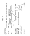
- FIG. 7 is a timing chart showing an operation sequence of the BOST board of FIG. 6 in the semiconductor device manufacturing process of the first embodiment
- FIG. 8 is a schematic diagram showing a hardware configuration of the test system used in the semiconductor device manufacturing process of the first embodiment
- FIG. 9 is a conceptual diagram showing a basic construction of a test system used in a semiconductor device manufacturing process according to a second embodiment of the present invention.
- FIG. 10 is a test flow diagram showing a simultaneous test method by whole-surface contact at a wafer level used in a semiconductor device manufacturing process having been studied as a process which the present invention premises;
- FIG. 11 is an explanatory diagram showing a test time sequence of the test flow of FIG. 10 in the semiconductor device manufacturing process having been studied as a process which the present invention premises.
- FIGS. 1 to 8 are for illustration of the process.
- FIG. 1 is a manufacturing flow chart showing the semiconductor device manufacturing process of this embodiment.
- This wafer processing step itself has no direct bearing on the present invention, so the details thereof will not be described here.
- wafer processings such as oxidation, application of a gate electrode material for example, selective etching, selective introduction of a conduction impurity, formation of an insulating layer, and formation of a wiring layer, are repeated for a semiconductor wafer provided such as a single crystal silicon, to form a desired integrated circuit.
- an electric contactor is brought into contact with plural chips, preferably all chips, on a wafer to test electric characteristics of the chips in parallel.
- burn-in in which semiconductor chips having a likelihood of becoming defective in future are subjected to screening
- a function test in which a memory function is tested by write and read operations using a predetermined test pattern to check whether operations are performed like predetermined functions
- DC tests such as open/short test between input and output terminals, leakage current test, and supply current test
- AC tests for testing AC timing in memory control are included burn-in in which semiconductor chips having a likelihood of becoming defective in future are subjected to screening, a function test in which a memory function is tested by write and read operations using a predetermined test pattern to check whether operations are performed like predetermined functions, DC tests such as open/short test between input and output terminals, leakage current test, and supply current test, and AC tests for testing AC timing in memory control.
- the thickness of the semiconductor wafer used is set at a relatively large value of about 300 to 400 ⁇ m. The reason why the semiconductor wafer is thus made relatively thick is as mentioned above.
- the back side i.e., the side opposite to a main surface on which circuit components are formed, of the wafer is subjected to grinding so as to give a desired thinness of the wafer.
- the wafer has been made relatively thick, so in this back grinding step is performed for grinding the wafer up to a thickness desired as product.
- the wafer is made as thin as 100 to 150 ⁇ m by back grinding.
- the wafer is diced chip by chip. As a result, the chips on the wafer are separated into individual chips.
- chips found to be good in test results of electric characteristics are shipped as products.
- chips of good quality may be conveyed to an assembling step for assembly into a package structure and thereafter the thus-assembled packages may be shipped as products.
- a die bonding step in which each chip is mounted on a package substrate, a wire bonding step in which pad electrodes on the chip and pad electrodes on the package substrate are electrically connected with each other through wires, a resin molding step in which the chip and the wires are subjected to molding with resin so as to be protected, and a lead molding step in which external leads are subjected to molding and surface treatment.
- the chips are also applicable to such a package structure as adopts flip chip bonding in which pads on each chip and pads on a substrate are connected together using bumps.
- FIG. 2 is a conceptual diagram showing the basic construction.
- the test system is made up of a wafer 2 , the wafer 2 having plural chip constituting portions 1 which are to become plural chips each constituting a flash memory for example (the chip constituting portions will hereinafter be referred to merely as “chips” to avoid complication of expression as noted earlier), a wafer level whole-surface contact device 3 for electric contact with the whole surface of the wafer 2 , i.e., for contact with all of electrodes required for testing the plural chips, a tester 4 for testing electric characteristics of the chips on the wafer 2 , and a BOST board 5 interposed between the tester 4 and the wafer level whole-surface contact device 3 and with a BOST (Built Out Self Test) circuit mounted thereon, the BOST circuit being constituted by a substrate with a chip-by-chip control circuit mounted thereon.
- a wafer level whole-surface contact device 3 for electric contact with the whole surface of the wafer 2 , i.e., for contact with all of electrodes required for testing the plural chips
- the BOST board 5 has functions which permit a decrease of tester load based on a decrease in the number of signals, E/W speed-up of a flash memory by execution of a forced acceleration test, self-test, self-repair, self-trimming, and MGM processing, although the details thereof will be described later.
- the plural chips 1 on the wafer 2 are each provided with plural pads (external terminals of each semiconductor chip), e.g., six pads.
- the flash memories to be tested are each provided with plural flash memory cells which are selected by address selection, a fuse for optimizing a read decision level in data read and a power supply circuit whose trimming condition is set by the fuse, and a fuse for a relief address corresponding to a defective memory cell and a corresponding relief circuit.
- first test involving plural operation steps which comprise erase, post erase, write, read, and decision under a first test condition
- second test involving the same plural steps as in the first test under a second test condition different from the first test condition
- third test comprising power trimming, blowing of fuse, voltage monitor, and decision
- fourth test comprising relief and decision.
- the first test may be understood to be a test conducted under a supply voltage which corresponds to a lower limit of an operating voltage to be guaranteed
- the second test may be understood to be a test conducted under a supply voltage corresponding to an upper limit of the operating voltage.
- the difference in test conditions between the first and second tests is not limited to one concerned with supply voltage, but can be set by changing the write data values or patterns in the respective write operations for example or by another change.
- “erase” is an erase operation for bringing the memory cell threshold voltage in each chip into an erase level for initialization. Though not specially limited, in the case where a chip serving as a flash memory has plural memory blocks, the erase is performed so that it can be done block by block in accordance with a command for block selection. “Post erase” is a weak rewrite operation for narrowing the threshold voltage distribution at the erase level. “Write” is a write operation for writing a voltage corresponding to “0” or “1” into a selected memory cell and making the threshold voltage level into a write level corresponding to “0” or “1”.
- addresses lying in a desired address range are indicated plural times from the exterior of the chip and the supply of write data for memory cells having the indicated addresses is performed.
- the write for test is not a combination of a single write and a single read, but is a sequential write for sequential addresses lying in the desired address range.
- Read is a read operation for reading the voltage level written in the write operation and judging whether the voltage level has reached one corresponding to “0” or “1.” Read is performed by sequential read address designation in a desired address range.
- “power trimming” is an operation for trimming, while shifting, the voltage generated from the power supply circuit in each chip 1 in accordance with the test result.
- “Blowing of fuse” is an operation for cutting a fuse corresponding to the trimming voltage.
- “Voltage monitor” is an operation for monitoring whether a desired trimming voltage is generated after cutting of the fuse. In this third operation, if the decision answer is negative, the operations beginning with power trimming are repeated and the test is completed upon occurrence of the desired trimming voltage (the decision answer is affirmative; Yes).
- “relief” is an operation for relieving a fail bit in each chip 1 in accordance with the test result.
- this relief operation for replacing the memory cell judged to be a fail bit in each chip 1 with a memory cell for redundancy, the fuse corresponding to the fail bit is cut and the fail bit is replaced with a redundancy bit.
- the relief operation if the decision answer is negative, the relief operation is repeated and the test is completed upon replacement of the fail bit with the redundancy bit (the decision answer is Yes).
- the test flow of FIG. 3 shows that the test is proceeded substantially independently for each of plural chips. This point will be described below in a successive manner.
- test flow according to this embodiment it is possible to effect a simultaneous test by whole-surface contact at the wafer level.
- This is the same as in the technique ( FIG. 10 ) which the present inventor has studied as a premise of the present invention.
- the test of each chip 1 is controlled individually by the BOST board 5 with chip-by-chip control circuits mounted thereon, so unlike the technique studied previously, when one chip 1 has gone through the test of one test item, a shift to the next test for that chip is not required to stand by until the end of test of the other chips 1 .
- test time sequence shown in FIG. 4 .
- test time sequence shown in FIG. 4 represents the execution of the test items of tests 1 , 2 , 3 , and 4 for conducting the first to fourth tests shown in FIG. 3 with respect to the chips 1 (# 1 ), (# 2 ), (# 3 ), . . . , (#N ⁇ 1), (#N) on the wafer 2 .
- test items are executed in the order of tests 1 , 2 , 3 , and 4 in such a manner that the end of a preceding test item is followed by the execution of the next test item.
- test end time differs depending on each chip 1 .
- the chip 1 (# 3 ) is the lowest in test end time in test 1 , namely, it is the worst chip.
- chip 1 (#N), chip 1 (# 1 ), and chip 1 (# 2 ) become worst chips in tests 2 , 3 , and 4 , respectively.
- FIG. 5 illustrates a test system
- the illustrated test system is made up of a wafer 2 , the wafer 2 having on a main surface thereof a plurality of chips 1 serving as flash memories respectively, a wafer level whole-surface contact device 3 for contact with the whole surface of the wafer 2 , a tester 4 for testing electric characteristics of each chip 1 , and a plurality of BOST boards 5 interposed between the tester 4 and the wafer level whole-surface contact device 3 .
- a general-purpose memory tester is used as the tester 4 and plural BOST boards 5 are placed between the tester and the wafer level whole-surface contact device 3 to permit a simultaneous test of all of the chips 1 present on the wafer 2 .
- Plural (Nb) BOST boards 5 are used, which make it possible to control ni pieces of chips 1 on the wafer 2 . That is, N number of chips 1 on the wafer 2 are controlled by Nb number of BOST boards 5 (Nb ⁇ N).
- BOST board 5 (# 1 ) is allocated to chips 1 (# 1 ) to (#ni).
- BOST board 5 (# 2 ) is allocated to chips 1 (#ni+1) to (#nj), . . .
- the last BOST board 5 (#Nb) is allocated to chips 1 (#nm+1) to (#N).
- the tester 4 is constructed so as to provide Test Start signal, Test Item designating information, Address Range information, Data Pattern, and Clock signal as common instructions to each BOST board 5 . Further, the tester 4 is constructed so as to receive such test result information as Test End signal and Chip Category information from each BOST board 5 . In other words, the tester 4 does not operate as such a commonly-used tester as forms various test signals for testing chips directly by itself and tests output signals from the chips on the basis of expected value information, but it controls each BOST board for test and obtains test results on the basis of information provided from each BOST board. Therefore, the tester 4 can be regarded as constituting a host tester or a test controller.
- each BOST board 5 The operation of each BOST board 5 is controlled in accordance with the foregoing control signals provided from the tester 4 , and each BOST board 5 provides signals corresponding to the above common instructions, voltage trimming information, and Forced Acceleration Voltage signal, as individual chip control information to each chip 1 through the wafer level whole-surface contact device 3 . Further, each BOST board 5 receives device output and Device Recognition signal from each chip 1 through the wafer level whole-surface contact device 3 .
- Each BOST board forms test result information by reference to signals provided from each chip and, upon completion of the testing operation, sends Test End signal and chip category information to the tester 4 , whereby it becomes possible for the tester 4 to recognize the test result of each chip 1 .
- each BOST board 5 is made up of a first input/output circuit (I/O circuit) 11 a disposed between the BOST board and the tester 4 , a second I/O circuit 11 b disposed between the BOST board 5 and the wafer level whole-surface contact device 3 , a CPU 12 which controls, for example, the execution of test in each chip 1 on the wafer 2 , a SRAM 13 which stores test information, trimming information, and relief information of each chip 1 , a trimming voltage generator 14 for trimming the power supply circuit in each chip 1 , a comparator 15 for comparing the test results of chips 1 and making a decision, a SRAM 16 and a relief information generator 17 for generating relief data to relieve a fail bit in each chip 1 , and a forced acceleration generator 18 for accelerating a specific test forcibly.
- I/O circuit input/output circuit
- the first and second I/O circuits 11 a , 11 b are interface circuits for interface between the tester 4 , as well as the wafer level whole-surface contact device 3 , and an internal circuit formed within the BOST board 5 .
- the first and second I/O circuits 11 a , 11 b are connected to the tester 4 and the wafer level whole-surface contact device 3 , while in the interior of the BOST board 5 they are connected to the CPU 12 , trimming voltage generator 14 , comparator 15 , relief information generator 17 , and forced acceleration voltage generator 18 .
- the first I/O circuit 11 a receives Test Start signal, Test Item Control signal (e.g., Erase, Write, Read), test address range information, and data pattern (e.g., all “0,” all “1”) as common instructions from the tester 4 , and provides signals (Address, Data, Control) corresponding to the common instructions, voltage trimming information (flash fuse write information), Forced Acceleration Voltage signal, and relief information (address) to each chip 1 . Further, the first I/O circuit 11 a provides Test End signal and chip category information (e.g., good/bad, mat/block defect) to the tester 4 .
- Test Item Control signal e.g., Erase, Write, Read
- test address range information e.g., all “0,” all “1”
- data pattern e.g., all “0,” all “1”
- signals Address, Data, Control
- voltage trimming information flash fuse write information
- Forced Acceleration Voltage signal e.g., Forced Acceleration Voltage signal
- the second I/O circuit 11 b receives device output and Device Recognition signal from each chip 1 and sends them to the CPU 12 and the comparator 15 .
- the CPU 12 is connected to the first and second I/O circuits 11 a , 11 b , SRAM 13 , trimming voltage generator 14 , comparator 15 , SRAM 16 , relief information generator 17 , and forced acceleration voltage generator 18 , and it is an information processing circuit which determines the state the test of each chip 1 on the wafer 2 and which instructs the execution of a test.
- the CPU 12 receives a Test Start signal, a Test Item Control signal, test address range information and a data pattern from the first I/O circuit 11 a , then provides signals corresponding to the foregoing common instructions, voltage trimming information, a Forced Acceleration Voltage signal, and relief information to each chip 1 through the second I/O circuit 11 b , and executes a test for each chip 1 . Moreover, the CPU 12 sends out trimming information to the trimming voltage generator 14 , provides a trimming voltage to each chip 1 through the second I/O circuit 11 b , and provides control so that there is performed a power trimming operation of each chip 1 .
- the CPU 12 compares it with an expected value in the comparator 15 and makes a pass/fail bit decision. As to a fail bit, the CPU 12 causes this information to be stored in SRAM 16 , then sends associated relief information to the relief information generator 17 , provides relief information to each chip 1 through the second I/O circuit 11 b , and provides makes control so that a fail bit relief operation is performed. As to a specific test, the CPU 12 provides control so that an acceleration voltage is fed to each chip 1 through the forced acceleration voltage generator 18 . Then, the CPU 12 sends a Test End signal and chip category information to the tester 4 through the first I/O circuit 11 a.
- the SRAM 13 is a memory circuit for the storage of test results of each chip 1 on the wafer 2 and for the storage of a trimming voltage and a fail bit address. It is connected to the CPU 12 . In the SRAM 13 , information on each chip 1 is stored as necessary on the basis of the execution of a test which is controlled by the CPU 12 .
- the trimming voltage generator 14 is a voltage generator which trims the power supply circuit in each chip 1 on the wafer 2 , and it is connected to I/O circuit 11 b and CPU 12 .
- the trimming voltage generator 14 generates a trimming voltage on the basis of the execution of a test controlled by the CPU 12 and in accordance with trimming information.
- the comparator 15 compares test results of chips 1 on the wafer 2 and makes a decision. It is connected to both I/O circuit 11 b and CPU 12 . In the comparator 15 , a device output of a test result provided from each chip 1 through the I/O circuit 11 b is compared with an expected value on the basis of the execution of the test controlled by the CPU 12 and a pass/fail bit decision is made.
- the SRAM 16 and the relief information generator 17 are relief circuits for the relief of a fail bit in each chip 1 on the wafer 2 .
- the SRAM 16 is connected to both CPU 12 and relief information generator 17 , while the relief information generator 17 is connected to the CPU 12 , SRAM 16 , and I/O circuit 11 b .
- the SRAM 16 stores relief information based on a fail bit.
- the relief information generator 17 provides relief information to each chip 1 through the I/O circuit 11 b on the basis of the relief information stored in SRAM 16 to perform a relief processing for the fail bit.
- the forced acceleration voltage generator 18 is a circuit for accelerating a specific test forcibly and it is connected to both CPU 12 and I/O circuit 11 b . On the basis of the execution of a test controlled by CPU 12 the forced acceleration voltage generator 18 generates an acceleration voltage for a specific test and provides it to each chip 1 through the I/O circuit 11 b.
- each BOST board 5 its second I/O circuit is required to have I/O terminals of such a number as corresponds to terminals of each of the chips to be tested simultaneously.
- the number of terminals required to be electrically contacted at the time of test by plural semiconductor chips which are formed on a single semiconductor wafer is often about ten thousand or more.
- the construction using plural BOST boards 5 is an appropriate construction in avoiding an increase in the number of terminals of the I/O circuit 11 b in each board and restricting the number of chips to be controlled by one CPU to facilitate the simultaneous independent test for plural chips. In other words, such a construction facilitates the formation of BOST boards.
- the BOST board 5 receives, as input signals from the tester 4 , a clock signal, CLK, and a test start signal, Test Start, which is synchronized with the clock signal CLK. Upon receipt of the Test Start signal the BOST board 5 generates Address, Data, and Control signals under the control of CPU 12 and outputs these signals to each chip 1 .
- the BOST board 5 receives, as input from each chip 1 , a device output of test result provided in response to Address, Data, and Control signals, then compares the device output with an expected value under the control of CPU 12 and makes a decision, then stores the result of the comparison and decision in SRAM 13 .
- the information stored in the SRAM 13 is used as trimming information by the trimming voltage generator 14 and as relief information by the relief information generator 17 .
- the BOST board 5 again outputs Address, Data, and Control signals to each chip 1 and receives a device output of test result from each chip, then if it is judged by the CPU 12 that the test is over, the BOST board 5 outputs the test result and a test end signal, Test End, to the tester 4 .
- FIG. 8 schematically illustrates the example.
- the test system is hardwarewise composed of a wafer level whole-surface contact device 3 for contact with the whole surface of the wafer 2 which comprises plural chips 1 with flash memory circuits formed thereon, a tester 4 constituted by a general-purpose memory tester for testing electric characteristics of each chip 1 on the wafer 2 , and a BOST board rack 21 incorporating plural BOST boards 5 which are connected between the tester 4 and the wafer level whole-surface contact device 3 .
- the BOST board 5 is constituted as follows.
- the functions of I/O circuits 11 a , 11 b , CPU 12 , SRAM 13 , trimming voltage generator 14 , comparator 15 , SPAM 16 , relief information generator 17 , and forced acceleration voltage generator 18 which have been explained above in connection with FIG. 6 , are implemented by ASIC such as FPGA and SRAM and these components are mounted on a substrate having board rack mounting terminals.
- the BOST board rack 21 is constituted so that it can receive therein plural BOST boards capable of being inserted and set.
- the tester 4 and the BOST board rack 21 are electrically connected with each other through such a cable as shown in the figure.
- the BOST board rack 21 and the wafer level whole-surface contact device 3 are connected together through a cable.
- FIG. 8 there is illustrated a method wherein the wafer level whole-surface contact device 3 uses a single wafer level contactor 22 to effect contact of all the chips 1 on one wafer 2 , a method of testing plural wafers 2 at a time is also applicable to the case where wafers 2 are packed one by one.
- the wafer 2 to be tested is formed with plural chips 1 .
- Each chip 1 is constructed so as to have six pads (external terminals) 23 for I/O, control, and power supply.
- An electric connection to each chip 1 is effected by the wafer level contactor 22 which is incorporated in the wafer level whole-surface contact device 3 .
- the wafer level contactor 22 is required to have a very large number of contactors so as to correspond to the pads of all the chips on the wafer 2 to be tested and is hence required to have such a fine size as can correspond to the pads of each chip.
- the contactor 22 is provided on one main surface thereof with probe projections 25 , i.e., contactors, which are formed of a metallic material.
- a metallic wiring layer extended to one main surface of the contactor is connected to the probe projections 25 , while to the metallic wiring layer are connected oblique holes formed through main surfaces of the substrate 24 and is also connected a metallic wiring layer extended to an opposite main surface of the substrate.
- An electric connection of the BOST board to the probe projections 25 is made by wiring connection to the metallic wiring layer formed on the opposite main surface of the substrate 24 .
- the portions opposed to the probe projections 25 are removed, whereby a certain flexibility is imparted to the substrate portions which support the probe projections, thereby ensuring a satisfactory contact irrespective of slight variations (change of distance) in the distance between the wafer surface to be tested and the contactor 22 which variations result from various factors.
- the wafer level whole-surface contact device 3 is provided on its body side with a test stage having a high flatness and the illustrated wafer 2 to be tested is placed on the test stage.
- the contactor 22 is supported by a support member which is mounted on the device body side to that it can be opened and closed.
- the wafer 2 is put on the body-side test stage and the contactor 22 is brought into contact with pads on the wafer by rotation of the support member.
- a load for attaining a satisfactory contact between the contactor 22 and the pads on the wafer 2 is provided by the support member or by a loading means (not shown).
- test is conducted in an environment in which the temperature and humidity of the entire surroundings of the wafer level whole-surface contact device are controlled.
- each test item is controlled chip by chip by the BOST board 5 inserted between the wafer 2 and the tester 4 and with a control circuit mounted thereon, so that the total test time for a single wafer 2 can be minimized.
- the resulting shortening of the test time permits reduction of the test cost and improvement of the throughput.
- FIG. 9 illustrates the process.
- the semiconductor device manufacturing process of this second embodiment also uses a wafer level whole-surface contact device for contact with the whole surface of a wafer, but, unlike the first embodiment, adopts a construction suitable for avoiding the simultaneous test of all the chips on wafer whenever necessary.
- a case where it is better to avoid the simultaneous test of all the chips on wafer occurs, for example, when the number of signal lines in each of plural chips is large and so, with a limited number of BOST boards, it is difficult to carry out the concurrent test of all the chips on wafer.
- the test system illustrated in FIG. 9 comprises a wafer 2 a with plural chips 1 a formed thereon which chips constitute flash memories, a wafer level whole-surface contact device 3 for contact with the whole surface of the wafer 2 a , a tester 4 for testing electric characteristics of each chip 1 a on the wafer 2 a , and a BOST board 5 as BOST means interposed between the tester 4 and the wafer level whole-surface contact device 3 and constituted by a substrate with chip-by-chip control circuits mounted thereon.
- the chips 1 a on the wafer 2 a to be tested are each provided with a relatively large number of pads, for example, 20 to 30 pads.
- the test system of this embodiment is constructed so as to be applicable also to the case where even if all signals are sent to the tester 4 , it is impossible to handle all of them, for example due to a large number of signal lines per chip 1 a on the wafer 2 a . More specifically, there is adopted a method wherein the concurrent test as in the first embodiment is performed for a set of plural chips 1 a out of all the chips 1 a on the wafer 2 , and after this set of chips 1 a have been tested for test items, test signals are fed to the other untested chips 1 a than the above set of chips, allowing the test to be carried out chip by chip.
- the BOST board 5 detects information of a chip 1 a the test of which has been completed earlier, and sends it to the tester 4 , which in turn starts testing another chip 1 a immediately in accordance with the signal. In this way there is obtained an effect close to the test time sequence effect shown in FIG. 4 in the first embodiment.
- a flash memory was referred to as an example in the above embodiments, the process of the present invention is also applicable effectively to a non-volatile memory such as EEPROM, a flash memory card, and a flash memory module, and further to a microcomputer which incorporates a flash memory.
Abstract
Description
- (1) A common test control signal is provided from a tester to a BOST (Built Out Self Test) circuit interposed between the tester and a wafer, and a test signal is fed from the BOST circuit to each chip on the wafer, whereby test is conducted chip by chip, further, another test is conducted simultaneously for plural chips on the wafer.
- (2) A common test control signal is fed to the BOST circuit interposed between the tester and the wafer and a test signal is fed from the BOST circuit to a first set of chips on the wafer to conduct test chip by chip, while another test is conducted simultaneously for plural chips out of the first set of chips on the wafer. Further, after the execution of test items for the first set of chips has been completed, a test signal is fed from the BOST circuit to chips other than the first set of chips. Thus, successively, after the end of execution of test items for chips to be tested, a test signal is fed to chips not tested yet and test items are executed chip by chip.
- (1) A first test comprising erase, post-erase, write, and read is conducted for chip 1 (#1) on wafer 2 (steps S201 to S204), followed by judgment as to whether the first test has been completed or not (S205), and upon completion of the first test, a shift is made to the execution of a second test. That is, a second test comprising erase, post-erase, write, and read is conducted (S206 to S210), and upon completion of the second test, a shift is made to a third test which comprises power trimming, blowing of fuse, voltage monitor, and decision (S211 to S214). Further, after the end of the third test, a shift is made to the execution of a fourth test which comprises relief and decision (S215 and S216). When the relief operation in the fourth test ends, the test of all test items for the chip 1 (#1) is over.
- (2) Also for the other chips 1 (#2) to (#N) on the
wafer 2, as is the case with the chip 1 (#1), in parallel with the chips 1(#2) to (#N), the first test comprising erase, posterase, write, read, and decision, the second test comprising erase, post-erase, write, read, and decision, the third test comprising power trimming, blowing of fuse, voltage monitor, and decision, and the fourth test comprising relief and decision, are conducted in such a manner that the end of a preceding test is followed by the execution of the next test (S221 to S236). In each of the chips 1 (#2) to (#N), the end of relief operation leads to the end of test of all the test items. - (3) When the test of all the items in chips 1 (#1) to (#N) on the
wafer 2 is over, all the tests for all the chips 1 (#1) to (#N) terminate (S241). Upon completion of the test for all the chips on the wafer, the test for onewafer 2 is completed.
- (1) In a semiconductor device with different test times of chips on wafer, each test item is controlled chip by chip by BOST means interposed between the wafer and the tester, whereby it becomes possible to minimize the total test time for a single wafer.
- (2) As a result of shortening of the test time per wafer mentioned in the above (1) it becomes possible to reduce the test cost of the semiconductor device and improve the throughput.
Claims (7)
Applications Claiming Priority (2)
| Application Number | Priority Date | Filing Date | Title |
|---|---|---|---|
| JP2001398832A JP2003197697A (en) | 2001-12-28 | 2001-12-28 | Method for manufacturing semiconductor device |
| JP2001-398832 | 2001-12-28 |
Publications (2)
| Publication Number | Publication Date |
|---|---|
| US20030121584A1 US20030121584A1 (en) | 2003-07-03 |
| US7024604B2 true US7024604B2 (en) | 2006-04-04 |
Family
ID=19189393
Family Applications (1)
| Application Number | Title | Priority Date | Filing Date |
|---|---|---|---|
| US10/274,144 Expired - Fee Related US7024604B2 (en) | 2001-12-28 | 2002-10-21 | Process for manufacturing semiconductor device |
Country Status (2)
| Country | Link |
|---|---|
| US (1) | US7024604B2 (en) |
| JP (1) | JP2003197697A (en) |
Cited By (2)
| Publication number | Priority date | Publication date | Assignee | Title |
|---|---|---|---|---|
| US20130176045A1 (en) * | 2009-07-03 | 2013-07-11 | Samsung Electronics Co., Ltd. | Package test devices having a printed circuit board |
| US20150206602A1 (en) * | 2014-01-17 | 2015-07-23 | Nuvoton Technology Corporation | Chip, operation method, and manufacturing method of electronic apparatus |
Families Citing this family (13)
| Publication number | Priority date | Publication date | Assignee | Title |
|---|---|---|---|---|
| JP2006179649A (en) * | 2004-12-22 | 2006-07-06 | Nec Electronics Corp | Device for inspecting memory device |
| US7528622B2 (en) | 2005-07-06 | 2009-05-05 | Optimal Test Ltd. | Methods for slow test time detection of an integrated circuit during parallel testing |
| JP2010078472A (en) * | 2008-09-26 | 2010-04-08 | Yokogawa Electric Corp | Semiconductor testing apparatus |
| KR101202020B1 (en) * | 2008-11-14 | 2012-11-16 | 한국전자통신연구원 | System and method for wafer level tuning of integrated circuit chips |
| US8112249B2 (en) | 2008-12-22 | 2012-02-07 | Optimaltest Ltd. | System and methods for parametric test time reduction |
| JP2011134410A (en) * | 2009-12-25 | 2011-07-07 | Toshiba Corp | Nonvolatile semiconductor memory device and test method of the same |
| TWI440114B (en) * | 2010-11-30 | 2014-06-01 | King Yuan Electronics Co Ltd | Wafer inspection system |
| CN103869630B (en) * | 2012-12-14 | 2015-09-23 | 北大方正集团有限公司 | A kind of pre-contraposition adjustment method |
| CN104237766B (en) * | 2013-06-24 | 2017-06-20 | 上海东软载波微电子有限公司 | Chip detecting method and device |
| US9607707B1 (en) * | 2016-06-30 | 2017-03-28 | Sandisk Technologies Llc | Weak erase prior to read |
| EP4318246A1 (en) * | 2021-03-23 | 2024-02-07 | Kioxia Corporation | Storage system |
| CN117396855A (en) * | 2021-09-02 | 2024-01-12 | 铠侠股份有限公司 | Storage system |
| CN115995260B (en) * | 2023-03-23 | 2023-08-11 | 长鑫存储技术有限公司 | Test method |
Citations (5)
| Publication number | Priority date | Publication date | Assignee | Title |
|---|---|---|---|---|
| US5241266A (en) * | 1992-04-10 | 1993-08-31 | Micron Technology, Inc. | Built-in test circuit connection for wafer level burnin and testing of individual dies |
| JPH06342600A (en) * | 1992-09-01 | 1994-12-13 | Matsushita Electric Ind Co Ltd | Semiconductor test device, semiconductor test circuit chip and probe card |
| US20020046374A1 (en) * | 1999-12-17 | 2002-04-18 | Hideyuki Aoki | Method of testing memory device, method of manufacturing memory device, apparatus for testing memory device, method of testing memory module, method of manufacturing memory module, apparatus for testing memory module and method of manufacturing computer |
| US20030038365A1 (en) * | 2001-08-22 | 2003-02-27 | Farnworth Warren M. | Substrate mapping |
| US6591385B1 (en) * | 2000-09-11 | 2003-07-08 | Agilent Technologies, Inc. | Method and apparatus for inserting programmable latency between address and data information in a memory tester |
-
2001
- 2001-12-28 JP JP2001398832A patent/JP2003197697A/en active Pending
-
2002
- 2002-10-21 US US10/274,144 patent/US7024604B2/en not_active Expired - Fee Related
Patent Citations (5)
| Publication number | Priority date | Publication date | Assignee | Title |
|---|---|---|---|---|
| US5241266A (en) * | 1992-04-10 | 1993-08-31 | Micron Technology, Inc. | Built-in test circuit connection for wafer level burnin and testing of individual dies |
| JPH06342600A (en) * | 1992-09-01 | 1994-12-13 | Matsushita Electric Ind Co Ltd | Semiconductor test device, semiconductor test circuit chip and probe card |
| US20020046374A1 (en) * | 1999-12-17 | 2002-04-18 | Hideyuki Aoki | Method of testing memory device, method of manufacturing memory device, apparatus for testing memory device, method of testing memory module, method of manufacturing memory module, apparatus for testing memory module and method of manufacturing computer |
| US6591385B1 (en) * | 2000-09-11 | 2003-07-08 | Agilent Technologies, Inc. | Method and apparatus for inserting programmable latency between address and data information in a memory tester |
| US20030038365A1 (en) * | 2001-08-22 | 2003-02-27 | Farnworth Warren M. | Substrate mapping |
Cited By (3)
| Publication number | Priority date | Publication date | Assignee | Title |
|---|---|---|---|---|
| US20130176045A1 (en) * | 2009-07-03 | 2013-07-11 | Samsung Electronics Co., Ltd. | Package test devices having a printed circuit board |
| US8832638B2 (en) * | 2009-07-03 | 2014-09-09 | Samsung Electronics Co., Ltd. | Package test devices having a printed circuit board |
| US20150206602A1 (en) * | 2014-01-17 | 2015-07-23 | Nuvoton Technology Corporation | Chip, operation method, and manufacturing method of electronic apparatus |
Also Published As
| Publication number | Publication date |
|---|---|
| US20030121584A1 (en) | 2003-07-03 |
| JP2003197697A (en) | 2003-07-11 |
Similar Documents
| Publication | Publication Date | Title |
|---|---|---|
| US7024604B2 (en) | Process for manufacturing semiconductor device | |
| JP3925839B2 (en) | Semiconductor memory device and test method thereof | |
| US6711075B2 (en) | Semiconductor wafer, semiconductor chip, and manufacturing method of semiconductor device | |
| US6625073B1 (en) | Apparatus and method for testing for defects between memory cells in packaged semiconductor memory devices | |
| US7941712B2 (en) | Method for error test, recordation and repair | |
| JP4308637B2 (en) | Semiconductor test equipment | |
| US7422914B2 (en) | Fabrication method of semiconductor integrated circuit device | |
| US6118711A (en) | Apparatus for testing redundant elements in a packaged semiconductor memory device | |
| US6181154B1 (en) | Method and apparatus for testing of dielectric defects in a packaged semiconductor memory device | |
| US7546506B2 (en) | DRAM stacked package, DIMM, and semiconductor manufacturing method | |
| US7940582B2 (en) | Integrated circuit that stores defective memory cell addresses | |
| JPH0574898A (en) | Manufacture of semiconductor devices | |
| JP2002163900A (en) | Semiconductor wafer, semiconductor chip, semiconductor device and producing method of semiconductor device | |
| US6661718B2 (en) | Testing device for testing a memory | |
| JPH09289234A (en) | Semiconductor device and its testing method, and testing jig for semiconductor device | |
| JP3031883B2 (en) | Inspection board capable of jointly inspecting integrated circuit devices operating in a merged data output mode and a standard operation mode | |
| US6352868B1 (en) | Method and apparatus for wafer level burn-in | |
| US6452845B1 (en) | Apparatus for testing redundant elements in a packaged semiconductor memory device | |
| US6721911B1 (en) | Method and apparatus for testing a memory array using compressed responses | |
| JP3603045B2 (en) | Semiconductor storage device, inspection jig thereof, and inspection method | |
| JP2003016798A (en) | Memory test method and multi-layer memory | |
| JPH10178073A (en) | Inspection method and production of semiconductor device | |
| JP2002280427A (en) | Semiconductor inspecting method and apparatus thereof | |
| JPH10284554A (en) | Semiconductor integrated circuit wafer and testing method therefor | |
| US20080219060A1 (en) | Device and method for internal voltage monitoring |
Legal Events
| Date | Code | Title | Description |
|---|---|---|---|
| AS | Assignment |
Owner name: HITACHI, LTD, JAPAN Free format text: ASSIGNMENT OF ASSIGNORS INTEREST;ASSIGNOR:AOKI, HIDEYUKI;REEL/FRAME:013408/0419 Effective date: 20020927 |
|
| AS | Assignment |
Owner name: RENESAS TECHNOLOGY CORPORATION, JAPAN Free format text: ASSIGNMENT OF ASSIGNORS INTEREST;ASSIGNOR:HITACHI, LTD.;REEL/FRAME:014573/0096 Effective date: 20030912 |
|
| AS | Assignment |
Owner name: RENESAS TECHNOLOGY CORPORATION, JAPAN Free format text: ASSIGNMENT OF ASSIGNORS INTEREST;ASSIGNOR:HITACHI, LTD.;REEL/FRAME:018559/0281 Effective date: 20030912 |
|
| FEPP | Fee payment procedure |
Free format text: PAYOR NUMBER ASSIGNED (ORIGINAL EVENT CODE: ASPN); ENTITY STATUS OF PATENT OWNER: LARGE ENTITY |
|
| FPAY | Fee payment |
Year of fee payment: 4 |
|
| AS | Assignment |
Owner name: RENESAS ELECTRONICS CORPORATION, JAPAN Free format text: MERGER;ASSIGNOR:RENESAS TECHNOLOGY CORP.;REEL/FRAME:024662/0280 Effective date: 20100416 |
|
| REMI | Maintenance fee reminder mailed | ||
| LAPS | Lapse for failure to pay maintenance fees | ||
| STCH | Information on status: patent discontinuation |
Free format text: PATENT EXPIRED DUE TO NONPAYMENT OF MAINTENANCE FEES UNDER 37 CFR 1.362 |
|
| FP | Lapsed due to failure to pay maintenance fee |
Effective date: 20140404 |