US7029945B2 - Organic field effect transistor with an organic dielectric - Google Patents
Organic field effect transistor with an organic dielectric Download PDFInfo
- Publication number
- US7029945B2 US7029945B2 US10/499,040 US49904004A US7029945B2 US 7029945 B2 US7029945 B2 US 7029945B2 US 49904004 A US49904004 A US 49904004A US 7029945 B2 US7029945 B2 US 7029945B2
- Authority
- US
- United States
- Prior art keywords
- insulating material
- field effect
- organic
- effect device
- permittivity insulating
- Prior art date
- Legal status (The legal status is an assumption and is not a legal conclusion. Google has not performed a legal analysis and makes no representation as to the accuracy of the status listed.)
- Expired - Lifetime
Links
- 0 *CC([CH+][CH2-])C* Chemical compound *CC([CH+][CH2-])C* 0.000 description 10
- CMXHEUQAFVDMIQ-UHFFFAOYSA-N C.CC1=CC=C(N(C2=CC=C(C3=CC=C(N(C4=CC=CC(C)=C4)C4=CC(C)=CC=C4)C=C3)C=C2)C2=CC=C(C3=CC=C(N(C4=CC=CC(C)=C4)C4=CC(C)=CC=C4)C=C3)C=C2)C=C1.CC1=CC=CC(N(C2=CC=C(C3=CC=C(N(C4=CC=CC=C4)C4=CC=C(C5=CC=C(N(C6=CC=CC=C6)C6=CC=C(C7=CC=C(N(C8=CC=CC(C)=C8)C8=CC(C)=CC=C8)C=C7)C=C6)C=C5)C=C4)C=C3)C=C2)C2=CC=CC(C)=C2)=C1 Chemical compound C.CC1=CC=C(N(C2=CC=C(C3=CC=C(N(C4=CC=CC(C)=C4)C4=CC(C)=CC=C4)C=C3)C=C2)C2=CC=C(C3=CC=C(N(C4=CC=CC(C)=C4)C4=CC(C)=CC=C4)C=C3)C=C2)C=C1.CC1=CC=CC(N(C2=CC=C(C3=CC=C(N(C4=CC=CC=C4)C4=CC=C(C5=CC=C(N(C6=CC=CC=C6)C6=CC=C(C7=CC=C(N(C8=CC=CC(C)=C8)C8=CC(C)=CC=C8)C=C7)C=C6)C=C5)C=C4)C=C3)C=C2)C2=CC=CC(C)=C2)=C1 CMXHEUQAFVDMIQ-UHFFFAOYSA-N 0.000 description 1
- IRNCYKLMPXTOAR-UHFFFAOYSA-N CC1=CC=C(N(C2=CC=C(C3=CC=C(N(C4=CC=CC=C4)C4=CC=C(C5=CC=C(N(C6=CC=CC=C6)C6=CC(C)=CC=C6)C=C5)C=C4)C=C3)C=C2)C2=CC=C(C3=CC=C(N(C4=CC=CC=C4)C4=CC=C(C5=CC=C(N(C6=CC=CC=C6)C6=CC(C)=CC=C6)C=C5)C=C4)C=C3)C=C2)C=C1.CC1=CC=CC(C(C2=CC=C(C3=CC=C(N(C4=CC=C(C5=CC=C(N(C6=CC=CC(C)=C6)C6=CC(C)=CC=C6)C=C5)C=C4)C4=CC=C(C5=CC=C(N(C6=CC=CC(C)=C6)C6=CC(C)=CC=C6)C=C5)C=C4)C=C3)C=C2)C2=CC=CC(C)=C2)=C1 Chemical compound CC1=CC=C(N(C2=CC=C(C3=CC=C(N(C4=CC=CC=C4)C4=CC=C(C5=CC=C(N(C6=CC=CC=C6)C6=CC(C)=CC=C6)C=C5)C=C4)C=C3)C=C2)C2=CC=C(C3=CC=C(N(C4=CC=CC=C4)C4=CC=C(C5=CC=C(N(C6=CC=CC=C6)C6=CC(C)=CC=C6)C=C5)C=C4)C=C3)C=C2)C=C1.CC1=CC=CC(C(C2=CC=C(C3=CC=C(N(C4=CC=C(C5=CC=C(N(C6=CC=CC(C)=C6)C6=CC(C)=CC=C6)C=C5)C=C4)C4=CC=C(C5=CC=C(N(C6=CC=CC(C)=C6)C6=CC(C)=CC=C6)C=C5)C=C4)C=C3)C=C2)C2=CC=CC(C)=C2)=C1 IRNCYKLMPXTOAR-UHFFFAOYSA-N 0.000 description 1
- CEKOIFADAHJOHQ-UHFFFAOYSA-N CC1=CC=CC(C2=CC=C(N(C3=CC=C(C4=CC=CC(C)=C4)C=C3)C3=C(C)C=C(C)C=C3)C=C2)=C1 Chemical compound CC1=CC=CC(C2=CC=C(N(C3=CC=C(C4=CC=CC(C)=C4)C=C3)C3=C(C)C=C(C)C=C3)C=C2)=C1 CEKOIFADAHJOHQ-UHFFFAOYSA-N 0.000 description 1
- CIUPZFNGBOQACP-UHFFFAOYSA-N CC1=CC=CC(C2=CC=C(N(C3=CC=C(C4=CC=CC(C)=C4)C=C3)C3=CC4=C(C=C3)C3=CC=CC=C3C4(C)C)C=C2)=C1 Chemical compound CC1=CC=CC(C2=CC=C(N(C3=CC=C(C4=CC=CC(C)=C4)C=C3)C3=CC4=C(C=C3)C3=CC=CC=C3C4(C)C)C=C2)=C1 CIUPZFNGBOQACP-UHFFFAOYSA-N 0.000 description 1
- PTSOWDWTNXIWLW-UHFFFAOYSA-N CCCCCCCCC1(CCCCCCCC)C2=CC(C)=CC=C2C2=C1C=C(C1=CC=C(C3=CC=C(C)S3)S1)C=C2 Chemical compound CCCCCCCCC1(CCCCCCCC)C2=CC(C)=CC=C2C2=C1C=C(C1=CC=C(C3=CC=C(C)S3)S1)C=C2 PTSOWDWTNXIWLW-UHFFFAOYSA-N 0.000 description 1
- FZXQGDAHMJFMSX-UHFFFAOYSA-N [H]C1=CC=C(N(C2=CC=C([H])C=C2)C2=C(C)C=C(C)C=C2)C=C1 Chemical compound [H]C1=CC=C(N(C2=CC=C([H])C=C2)C2=C(C)C=C(C)C=C2)C=C1 FZXQGDAHMJFMSX-UHFFFAOYSA-N 0.000 description 1
Images


Classifications
-
- H—ELECTRICITY
- H10—SEMICONDUCTOR DEVICES; ELECTRIC SOLID-STATE DEVICES NOT OTHERWISE PROVIDED FOR
- H10K—ORGANIC ELECTRIC SOLID-STATE DEVICES
- H10K10/00—Organic devices specially adapted for rectifying, amplifying, oscillating or switching; Organic capacitors or resistors having a potential-jump barrier or a surface barrier
- H10K10/40—Organic transistors
- H10K10/46—Field-effect transistors, e.g. organic thin-film transistors [OTFT]
- H10K10/462—Insulated gate field-effect transistors [IGFETs]
- H10K10/468—Insulated gate field-effect transistors [IGFETs] characterised by the gate dielectrics
- H10K10/471—Insulated gate field-effect transistors [IGFETs] characterised by the gate dielectrics the gate dielectric comprising only organic materials
-
- C—CHEMISTRY; METALLURGY
- C09—DYES; PAINTS; POLISHES; NATURAL RESINS; ADHESIVES; COMPOSITIONS NOT OTHERWISE PROVIDED FOR; APPLICATIONS OF MATERIALS NOT OTHERWISE PROVIDED FOR
- C09B—ORGANIC DYES OR CLOSELY-RELATED COMPOUNDS FOR PRODUCING DYES, e.g. PIGMENTS; MORDANTS; LAKES
- C09B57/00—Other synthetic dyes of known constitution
- C09B57/008—Triarylamine dyes containing no other chromophores
-
- C—CHEMISTRY; METALLURGY
- C09—DYES; PAINTS; POLISHES; NATURAL RESINS; ADHESIVES; COMPOSITIONS NOT OTHERWISE PROVIDED FOR; APPLICATIONS OF MATERIALS NOT OTHERWISE PROVIDED FOR
- C09B—ORGANIC DYES OR CLOSELY-RELATED COMPOUNDS FOR PRODUCING DYES, e.g. PIGMENTS; MORDANTS; LAKES
- C09B69/00—Dyes not provided for by a single group of this subclass
- C09B69/10—Polymeric dyes; Reaction products of dyes with monomers or with macromolecular compounds
- C09B69/109—Polymeric dyes; Reaction products of dyes with monomers or with macromolecular compounds containing other specific dyes
-
- H—ELECTRICITY
- H01—ELECTRIC ELEMENTS
- H01L—SEMICONDUCTOR DEVICES NOT COVERED BY CLASS H10
- H01L21/00—Processes or apparatus adapted for the manufacture or treatment of semiconductor or solid state devices or of parts thereof
- H01L21/02—Manufacture or treatment of semiconductor devices or of parts thereof
- H01L21/02104—Forming layers
- H01L21/02107—Forming insulating materials on a substrate
- H01L21/02109—Forming insulating materials on a substrate characterised by the type of layer, e.g. type of material, porous/non-porous, pre-cursors, mixtures or laminates
- H01L21/02112—Forming insulating materials on a substrate characterised by the type of layer, e.g. type of material, porous/non-porous, pre-cursors, mixtures or laminates characterised by the material of the layer
- H01L21/02118—Forming insulating materials on a substrate characterised by the type of layer, e.g. type of material, porous/non-porous, pre-cursors, mixtures or laminates characterised by the material of the layer carbon based polymeric organic or inorganic material, e.g. polyimides, poly cyclobutene or PVC
- H01L21/0212—Forming insulating materials on a substrate characterised by the type of layer, e.g. type of material, porous/non-porous, pre-cursors, mixtures or laminates characterised by the material of the layer carbon based polymeric organic or inorganic material, e.g. polyimides, poly cyclobutene or PVC the material being fluoro carbon compounds, e.g.(CFx) n, (CHxFy) n or polytetrafluoroethylene
-
- H—ELECTRICITY
- H01—ELECTRIC ELEMENTS
- H01L—SEMICONDUCTOR DEVICES NOT COVERED BY CLASS H10
- H01L21/00—Processes or apparatus adapted for the manufacture or treatment of semiconductor or solid state devices or of parts thereof
- H01L21/02—Manufacture or treatment of semiconductor devices or of parts thereof
- H01L21/02104—Forming layers
- H01L21/02107—Forming insulating materials on a substrate
- H01L21/02225—Forming insulating materials on a substrate characterised by the process for the formation of the insulating layer
- H01L21/0226—Forming insulating materials on a substrate characterised by the process for the formation of the insulating layer formation by a deposition process
- H01L21/02282—Forming insulating materials on a substrate characterised by the process for the formation of the insulating layer formation by a deposition process liquid deposition, e.g. spin-coating, sol-gel techniques, spray coating
-
- H—ELECTRICITY
- H10—SEMICONDUCTOR DEVICES; ELECTRIC SOLID-STATE DEVICES NOT OTHERWISE PROVIDED FOR
- H10K—ORGANIC ELECTRIC SOLID-STATE DEVICES
- H10K10/00—Organic devices specially adapted for rectifying, amplifying, oscillating or switching; Organic capacitors or resistors having a potential-jump barrier or a surface barrier
- H10K10/40—Organic transistors
- H10K10/46—Field-effect transistors, e.g. organic thin-film transistors [OTFT]
- H10K10/462—Insulated gate field-effect transistors [IGFETs]
- H10K10/464—Lateral top-gate IGFETs comprising only a single gate
-
- H—ELECTRICITY
- H10—SEMICONDUCTOR DEVICES; ELECTRIC SOLID-STATE DEVICES NOT OTHERWISE PROVIDED FOR
- H10K—ORGANIC ELECTRIC SOLID-STATE DEVICES
- H10K10/00—Organic devices specially adapted for rectifying, amplifying, oscillating or switching; Organic capacitors or resistors having a potential-jump barrier or a surface barrier
- H10K10/40—Organic transistors
- H10K10/46—Field-effect transistors, e.g. organic thin-film transistors [OTFT]
- H10K10/462—Insulated gate field-effect transistors [IGFETs]
- H10K10/466—Lateral bottom-gate IGFETs comprising only a single gate
-
- H—ELECTRICITY
- H10—SEMICONDUCTOR DEVICES; ELECTRIC SOLID-STATE DEVICES NOT OTHERWISE PROVIDED FOR
- H10K—ORGANIC ELECTRIC SOLID-STATE DEVICES
- H10K10/00—Organic devices specially adapted for rectifying, amplifying, oscillating or switching; Organic capacitors or resistors having a potential-jump barrier or a surface barrier
- H10K10/40—Organic transistors
- H10K10/46—Field-effect transistors, e.g. organic thin-film transistors [OTFT]
- H10K10/462—Insulated gate field-effect transistors [IGFETs]
- H10K10/468—Insulated gate field-effect transistors [IGFETs] characterised by the gate dielectrics
- H10K10/474—Insulated gate field-effect transistors [IGFETs] characterised by the gate dielectrics the gate dielectric comprising a multilayered structure
- H10K10/476—Insulated gate field-effect transistors [IGFETs] characterised by the gate dielectrics the gate dielectric comprising a multilayered structure comprising at least one organic layer and at least one inorganic layer
-
- C—CHEMISTRY; METALLURGY
- C08—ORGANIC MACROMOLECULAR COMPOUNDS; THEIR PREPARATION OR CHEMICAL WORKING-UP; COMPOSITIONS BASED THEREON
- C08G—MACROMOLECULAR COMPOUNDS OBTAINED OTHERWISE THAN BY REACTIONS ONLY INVOLVING UNSATURATED CARBON-TO-CARBON BONDS
- C08G2261/00—Macromolecular compounds obtained by reactions forming a carbon-to-carbon link in the main chain of the macromolecule
- C08G2261/10—Definition of the polymer structure
- C08G2261/11—Homopolymers
-
- C—CHEMISTRY; METALLURGY
- C08—ORGANIC MACROMOLECULAR COMPOUNDS; THEIR PREPARATION OR CHEMICAL WORKING-UP; COMPOSITIONS BASED THEREON
- C08G—MACROMOLECULAR COMPOUNDS OBTAINED OTHERWISE THAN BY REACTIONS ONLY INVOLVING UNSATURATED CARBON-TO-CARBON BONDS
- C08G2261/00—Macromolecular compounds obtained by reactions forming a carbon-to-carbon link in the main chain of the macromolecule
- C08G2261/10—Definition of the polymer structure
- C08G2261/12—Copolymers
-
- C—CHEMISTRY; METALLURGY
- C08—ORGANIC MACROMOLECULAR COMPOUNDS; THEIR PREPARATION OR CHEMICAL WORKING-UP; COMPOSITIONS BASED THEREON
- C08G—MACROMOLECULAR COMPOUNDS OBTAINED OTHERWISE THAN BY REACTIONS ONLY INVOLVING UNSATURATED CARBON-TO-CARBON BONDS
- C08G2261/00—Macromolecular compounds obtained by reactions forming a carbon-to-carbon link in the main chain of the macromolecule
- C08G2261/30—Monomer units or repeat units incorporating structural elements in the main chain
- C08G2261/31—Monomer units or repeat units incorporating structural elements in the main chain incorporating aromatic structural elements in the main chain
- C08G2261/314—Condensed aromatic systems, e.g. perylene, anthracene or pyrene
- C08G2261/3142—Condensed aromatic systems, e.g. perylene, anthracene or pyrene fluorene-based, e.g. fluorene, indenofluorene, or spirobifluorene
-
- C—CHEMISTRY; METALLURGY
- C08—ORGANIC MACROMOLECULAR COMPOUNDS; THEIR PREPARATION OR CHEMICAL WORKING-UP; COMPOSITIONS BASED THEREON
- C08G—MACROMOLECULAR COMPOUNDS OBTAINED OTHERWISE THAN BY REACTIONS ONLY INVOLVING UNSATURATED CARBON-TO-CARBON BONDS
- C08G2261/00—Macromolecular compounds obtained by reactions forming a carbon-to-carbon link in the main chain of the macromolecule
- C08G2261/30—Monomer units or repeat units incorporating structural elements in the main chain
- C08G2261/31—Monomer units or repeat units incorporating structural elements in the main chain incorporating aromatic structural elements in the main chain
- C08G2261/316—Monomer units or repeat units incorporating structural elements in the main chain incorporating aromatic structural elements in the main chain bridged by heteroatoms, e.g. N, P, Si or B
- C08G2261/3162—Arylamines
-
- C—CHEMISTRY; METALLURGY
- C08—ORGANIC MACROMOLECULAR COMPOUNDS; THEIR PREPARATION OR CHEMICAL WORKING-UP; COMPOSITIONS BASED THEREON
- C08G—MACROMOLECULAR COMPOUNDS OBTAINED OTHERWISE THAN BY REACTIONS ONLY INVOLVING UNSATURATED CARBON-TO-CARBON BONDS
- C08G2261/00—Macromolecular compounds obtained by reactions forming a carbon-to-carbon link in the main chain of the macromolecule
- C08G2261/30—Monomer units or repeat units incorporating structural elements in the main chain
- C08G2261/32—Monomer units or repeat units incorporating structural elements in the main chain incorporating heteroaromatic structural elements in the main chain
- C08G2261/322—Monomer units or repeat units incorporating structural elements in the main chain incorporating heteroaromatic structural elements in the main chain non-condensed
- C08G2261/3223—Monomer units or repeat units incorporating structural elements in the main chain incorporating heteroaromatic structural elements in the main chain non-condensed containing one or more sulfur atoms as the only heteroatom, e.g. thiophene
-
- C—CHEMISTRY; METALLURGY
- C08—ORGANIC MACROMOLECULAR COMPOUNDS; THEIR PREPARATION OR CHEMICAL WORKING-UP; COMPOSITIONS BASED THEREON
- C08G—MACROMOLECULAR COMPOUNDS OBTAINED OTHERWISE THAN BY REACTIONS ONLY INVOLVING UNSATURATED CARBON-TO-CARBON BONDS
- C08G2261/00—Macromolecular compounds obtained by reactions forming a carbon-to-carbon link in the main chain of the macromolecule
- C08G2261/90—Applications
- C08G2261/92—TFT applications
-
- H—ELECTRICITY
- H01—ELECTRIC ELEMENTS
- H01L—SEMICONDUCTOR DEVICES NOT COVERED BY CLASS H10
- H01L21/00—Processes or apparatus adapted for the manufacture or treatment of semiconductor or solid state devices or of parts thereof
- H01L21/02—Manufacture or treatment of semiconductor devices or of parts thereof
- H01L21/02104—Forming layers
- H01L21/02107—Forming insulating materials on a substrate
- H01L21/02109—Forming insulating materials on a substrate characterised by the type of layer, e.g. type of material, porous/non-porous, pre-cursors, mixtures or laminates
- H01L21/02112—Forming insulating materials on a substrate characterised by the type of layer, e.g. type of material, porous/non-porous, pre-cursors, mixtures or laminates characterised by the material of the layer
- H01L21/02172—Forming insulating materials on a substrate characterised by the type of layer, e.g. type of material, porous/non-porous, pre-cursors, mixtures or laminates characterised by the material of the layer the material containing at least one metal element, e.g. metal oxides, metal nitrides, metal oxynitrides or metal carbides
- H01L21/02175—Forming insulating materials on a substrate characterised by the type of layer, e.g. type of material, porous/non-porous, pre-cursors, mixtures or laminates characterised by the material of the layer the material containing at least one metal element, e.g. metal oxides, metal nitrides, metal oxynitrides or metal carbides characterised by the metal
- H01L21/02183—Forming insulating materials on a substrate characterised by the type of layer, e.g. type of material, porous/non-porous, pre-cursors, mixtures or laminates characterised by the material of the layer the material containing at least one metal element, e.g. metal oxides, metal nitrides, metal oxynitrides or metal carbides characterised by the metal the material containing tantalum, e.g. Ta2O5
-
- H—ELECTRICITY
- H01—ELECTRIC ELEMENTS
- H01L—SEMICONDUCTOR DEVICES NOT COVERED BY CLASS H10
- H01L21/00—Processes or apparatus adapted for the manufacture or treatment of semiconductor or solid state devices or of parts thereof
- H01L21/02—Manufacture or treatment of semiconductor devices or of parts thereof
- H01L21/02104—Forming layers
- H01L21/02107—Forming insulating materials on a substrate
- H01L21/02109—Forming insulating materials on a substrate characterised by the type of layer, e.g. type of material, porous/non-porous, pre-cursors, mixtures or laminates
- H01L21/02112—Forming insulating materials on a substrate characterised by the type of layer, e.g. type of material, porous/non-porous, pre-cursors, mixtures or laminates characterised by the material of the layer
- H01L21/02172—Forming insulating materials on a substrate characterised by the type of layer, e.g. type of material, porous/non-porous, pre-cursors, mixtures or laminates characterised by the material of the layer the material containing at least one metal element, e.g. metal oxides, metal nitrides, metal oxynitrides or metal carbides
- H01L21/02175—Forming insulating materials on a substrate characterised by the type of layer, e.g. type of material, porous/non-porous, pre-cursors, mixtures or laminates characterised by the material of the layer the material containing at least one metal element, e.g. metal oxides, metal nitrides, metal oxynitrides or metal carbides characterised by the metal
- H01L21/02186—Forming insulating materials on a substrate characterised by the type of layer, e.g. type of material, porous/non-porous, pre-cursors, mixtures or laminates characterised by the material of the layer the material containing at least one metal element, e.g. metal oxides, metal nitrides, metal oxynitrides or metal carbides characterised by the metal the material containing titanium, e.g. TiO2
-
- H—ELECTRICITY
- H01—ELECTRIC ELEMENTS
- H01L—SEMICONDUCTOR DEVICES NOT COVERED BY CLASS H10
- H01L21/00—Processes or apparatus adapted for the manufacture or treatment of semiconductor or solid state devices or of parts thereof
- H01L21/02—Manufacture or treatment of semiconductor devices or of parts thereof
- H01L21/04—Manufacture or treatment of semiconductor devices or of parts thereof the devices having at least one potential-jump barrier or surface barrier, e.g. PN junction, depletion layer or carrier concentration layer
- H01L21/18—Manufacture or treatment of semiconductor devices or of parts thereof the devices having at least one potential-jump barrier or surface barrier, e.g. PN junction, depletion layer or carrier concentration layer the devices having semiconductor bodies comprising elements of Group IV of the Periodic System or AIIIBV compounds with or without impurities, e.g. doping materials
- H01L21/30—Treatment of semiconductor bodies using processes or apparatus not provided for in groups H01L21/20 - H01L21/26
- H01L21/31—Treatment of semiconductor bodies using processes or apparatus not provided for in groups H01L21/20 - H01L21/26 to form insulating layers thereon, e.g. for masking or by using photolithographic techniques; After treatment of these layers; Selection of materials for these layers
- H01L21/312—Organic layers, e.g. photoresist
- H01L21/3127—Layers comprising fluoro (hydro)carbon compounds, e.g. polytetrafluoroethylene
-
- H—ELECTRICITY
- H01—ELECTRIC ELEMENTS
- H01L—SEMICONDUCTOR DEVICES NOT COVERED BY CLASS H10
- H01L28/00—Passive two-terminal components without a potential-jump or surface barrier for integrated circuits; Details thereof; Multistep manufacturing processes therefor
- H01L28/40—Capacitors
- H01L28/55—Capacitors with a dielectric comprising a perovskite structure material
- H01L28/56—Capacitors with a dielectric comprising a perovskite structure material the dielectric comprising two or more layers, e.g. comprising buffer layers, seed layers, gradient layers
-
- H—ELECTRICITY
- H10—SEMICONDUCTOR DEVICES; ELECTRIC SOLID-STATE DEVICES NOT OTHERWISE PROVIDED FOR
- H10K—ORGANIC ELECTRIC SOLID-STATE DEVICES
- H10K85/00—Organic materials used in the body or electrodes of devices covered by this subclass
- H10K85/10—Organic polymers or oligomers
- H10K85/111—Organic polymers or oligomers comprising aromatic, heteroaromatic, or aryl chains, e.g. polyaniline, polyphenylene or polyphenylene vinylene
- H10K85/113—Heteroaromatic compounds comprising sulfur or selene, e.g. polythiophene
- H10K85/1135—Polyethylene dioxythiophene [PEDOT]; Derivatives thereof
-
- H—ELECTRICITY
- H10—SEMICONDUCTOR DEVICES; ELECTRIC SOLID-STATE DEVICES NOT OTHERWISE PROVIDED FOR
- H10K—ORGANIC ELECTRIC SOLID-STATE DEVICES
- H10K85/00—Organic materials used in the body or electrodes of devices covered by this subclass
- H10K85/10—Organic polymers or oligomers
- H10K85/111—Organic polymers or oligomers comprising aromatic, heteroaromatic, or aryl chains, e.g. polyaniline, polyphenylene or polyphenylene vinylene
- H10K85/115—Polyfluorene; Derivatives thereof
-
- H—ELECTRICITY
- H10—SEMICONDUCTOR DEVICES; ELECTRIC SOLID-STATE DEVICES NOT OTHERWISE PROVIDED FOR
- H10K—ORGANIC ELECTRIC SOLID-STATE DEVICES
- H10K85/00—Organic materials used in the body or electrodes of devices covered by this subclass
- H10K85/10—Organic polymers or oligomers
- H10K85/151—Copolymers
-
- H—ELECTRICITY
- H10—SEMICONDUCTOR DEVICES; ELECTRIC SOLID-STATE DEVICES NOT OTHERWISE PROVIDED FOR
- H10K—ORGANIC ELECTRIC SOLID-STATE DEVICES
- H10K85/00—Organic materials used in the body or electrodes of devices covered by this subclass
- H10K85/60—Organic compounds having low molecular weight
- H10K85/615—Polycyclic condensed aromatic hydrocarbons, e.g. anthracene
-
- H—ELECTRICITY
- H10—SEMICONDUCTOR DEVICES; ELECTRIC SOLID-STATE DEVICES NOT OTHERWISE PROVIDED FOR
- H10K—ORGANIC ELECTRIC SOLID-STATE DEVICES
- H10K85/00—Organic materials used in the body or electrodes of devices covered by this subclass
- H10K85/60—Organic compounds having low molecular weight
- H10K85/631—Amine compounds having at least two aryl rest on at least one amine-nitrogen atom, e.g. triphenylamine
Definitions
- This invention relates to organic field effect transistors (OFETS) and processes for their manufacture.
- FET Field effect transistors
- a typical FET consists of a number of layers and they can be configured in various ways.
- an FET may comprise a substrate, an insulator, a semiconductor, source and drain electrodes connected to the semiconductor and a gate electrode adjacent the insulator.
- source and drain electrodes connected to the semiconductor and a gate electrode adjacent the insulator.
- charge carriers are accumulated in the semiconductor at its interface with the insulator.
- a conductive channel is formed between the source and the drain and a current will flow if a potential is applied to the drain.
- the present invention provides new and improved organic FETs and techniques to fabricate high quality organic transistors. It is also the purpose of the present invention to provide techniques to improve the semiconductor-insulator interface by the choice of materials and preparation conditions. In particular the present invention concerns the insulating material used in organic FETs.
- Wittmann and Smith (Nature 1991, 352, 414,) describe a technique of orienting organic materials on an oriented PTFE substrate.
- the PTFE is oriented by sliding a bar of solid PTFE on a hot substrate.
- This technique is applied in U.S. Pat. No. 5,912,473 (Matsushita, 1999, also U.S. Pat. No. 5,556,706 and U.S. Pat. No. 5,546,889) to use the PTFE oriented film as a substrate for depositing organic semiconductors in the manufacture of field effect transistors.
- the organic semiconductor also becomes oriented resulting in a higher carrier mobility.
- the PTFE layer is deposited according to the technique of Wittmann and Smith, i.e. sliding solid PTFE on the hot substrate.
- JP7221367 (Matsushita, 1995) describes a technique for the orientation of thiophene oligomers by the use of an oriented polymer substrate.
- the polymer substrate can be a solution coated amorphous perfluoropolymer, which is rubbed to induce orientation.
- the document teaches the use of the perfluoropolymer as an alignment layer.
- the gate insulator material the document suggests cyano ethyl pullulane, a cyano ethyl cellulose, polyvinyl alcohol, SiO 2 , Ta 2 O 5 .
- U.S. Pat. No. 5,612,228 claims complementary FET circuits with p-type organic and n-type inorganic materials.
- the n and p materials are deposited onto the same gate insulator using a bottom gate configuration.
- the organic semiconductor may be polyimide, polyphenylenevinylene, phthalocyanine, liquid crystal polymer or sexithiophene.
- the insulator may be “any convenient dielectric media such as SiO x , SiN x , AlO x as well as organic dielectric media such as polyimides, polyacrylates, poly(vinyl chloride), perfluoropolymers and liquid crystal polymers”. The disclosure does not teach what polymer properties would be most important.
- EP0786820 (Motorola, 1997) describes organic FETs with enhanced mobility by the use of orientation layers.
- orientation films rubbed polyimides, perfluoropolymers, and liquid crystal polymers are suggested.
- the invention suggests that the gate insulator may be “materials selected from inorganic dielectric media such as SiO x , SiN x and AlO x , as well as organic dielectric media such as polyimides, polyacrylates, poly(vinyl chloride), perfluoropolymers and liquid crystal polymers”. The disclosure does not teach what polymer properties would be most important.
- WO0147043 (Plastic Logic, 2001) describe organic FETs in which the gate insulator is polyvinylphenol (PVP), polyvinylalcohol (PVA), or polymethylmethacrylate (PMMA).
- the insulator is ink-jet printed from a solution of the material in a polar solvent to avoid dissolution or swelling of the underlying semiconductor.
- the document also describes organic FETs in which the gate insulator comprises more than one layer. In these cases non polar polymers are deposited between the polar insulator and PEDOT/PSS conductive gate electrode to prevent the diffusion of ions through the polar gate insulator. Also, surface modification layers are used on top of the non-polar polymers to enhance the wetting of the PEDOT/PSS dispersion however, in all cases the insulator layer adjacent to the semiconductor is either PVP, PVA, or PMMA.
- BCB benzocyclobutene
- SiO 2 SiO 2
- Parylene C polyimide gate insulators.
- BCB has a dielectric constant of 2.65, and it can be solution deposited, but it requires curing at high temperatures (200° C.). This makes the process incompatible with plastic substrates such as polyethylenenaphthalate or polyethyleneterephthalate and therefore is not preferred. Vapour deposition of the OSC is also not preferred as it is difficult to apply on large areas.
- polar groups of high permittivity insulators introduce random traps on localised states of the semiconductor through attraction of the charge carriers.
- Disordered or semi-disordered organic semiconductors e.g. many organic semiconductors deposited by solution coating techniques, have a high density of localised states and electron or hole hopping is a limiting factor in charge transport.
- charge transport in, e.g. highly ordered, materials with mobilities close to 0.1 cm 2 /V s begins to be reminiscent of band transport because such materials have a higher degree of ordering.
- the random dipole fields of high permittivity insulators have much lower influence on an electronic band where carriers are delocalised over large distances.
- the prior art techniques solve interface trapping by using a high permittivity insulator to fill up interface traps easily by inducing high charge densities.
- insulators of low permittivity in the gate insulator layer solves the problem of interface trapping by eliminating the traps themselves and yields much better performance with organic semiconductors, particularly, but not exclusively, disordered or semi-disordered organic semiconductors. Since many solution coatable materials have some degree of disorder and localised states are present, there is a benefit in using certain low permittivity insulators to avoid the modulation of site energies by random dipole moments. It should be noted, however, that even with the best possible alignment processes available, organic semiconductors are still essentially disordered such that the use of low permittivity insulators may be beneficial.
- FETs could be fabricated of very high quality, reproducibility, field effect mobility and extremely low hysteresis normally caused by interface trapping.
- high quality transistors can be obtained with very low dependence of the mobility on gate field.
- Low permittivity materials lead to lower gate capacitance, reducing the number of induced carriers.
- it has only a linear effect on the drain current and is easily compensated for by the reduction in interface trapping with the potential to increase carrier mobility significantly.
- an organic field effect device manufactured by the process of the first aspect of the invention.
- FIGS. 1 a )– d ) are cross sectional views of 4 possible configurations for a FET of the present invention.
- FIGS. 1 a ) and b ) have a bottom gate configuration and
- FIGS. 1 c ) and d ) have a top gate configuration.
- FIGS. 2 a )– d ) are a cross-sectional views of 4 possible configurations of an FET of the present invention where two gate insulator layers are present.
- FIGS. 2 a ) and b ) have a bottom gate configuration and
- FIGS. 2 c ) and d ) have a top gate configuration.
- layer 1 is a substrate
- layer 2 is an insulator
- layer 3 is an organic semiconductor
- S and D are source and drain electrodes
- G is the gate electrode.
- item 2 a is a second insulator layer.
- the invention may comprise depositing at least one high permittivity insulator layer on the other side of the low permittivity insulator layer from the organic semiconductor, to form a further part of the gate insulator.
- the at least one high permittivity insulator layer preferably has a higher permittivity than the low permittivity insulator layer.
- the at least one high permittivity insulator layer has a relative permittivity of 3.5 or higher, more preferably 10 or higher, and most preferably 20 or higher. The highest possible permittivity is preferred.
- the permittivity may range up to about 200.
- the at least one high permittivity insulator layer is also deposited from a solution.
- the organic semiconductor layer and/or the layer(s) of the gate insulator may be deposited from solution by spin coating.
- the whole process of manufacturing the device may be performed at or below about 100° C., thus making the process much less difficult to carry out than prior art manufacturing processes.
- both the organic semiconductor layer and the gate insulator layer(s) are deposited from solution large areas can be coated readily.
- the low permittivity gate insulator layer it has been found that even if the organic semiconductor layer is disordered or semi-ordered good mobilities are achieved.
- the gate insulator layer comprises an organic material, e.g. a polymer.
- an FET structure of FIG. 1 c is prepared by spin coating the semiconductor onto the substrate with pre-patterned drain and source electrodes. Next, an insulator in the form of a low permittivity polymer of relative permittivity below 3 is spin coated onto the semiconductor followed by the deposition of the gate electrode by vacuum evaporation or liquid deposition of a conductive solution or dispersion. It will be appreciated that the order of process steps may be altered to achieve structures a, b or d shown in FIG. 1 . It will be appreciated that the OFET could also have a vertical structure.
- the low permittivity organic insulator should have a conductivity less than 10 ⁇ 6 Scm ⁇ 1 to avoid leakage to the gate.
- Preferred insulators are materials of low polarity. It is desirable that the low frequency (measured between 50 to 10,000 Hz) permittivity (dielectric constant) g of the material should be below 3.0, and preferably 1.1 or greater. The permittivity is more preferably in the range 1.3–2.5, and especially in the range 1.5 to 2.1. A further preferred lower limit on the permittivity is 1.7. Such materials have few permanent dipoles, which could otherwise enhance localisation of charges on molecular sites at the interface with the semiconductor.
- the permittivity (dielectric constant) can be determined by the ASTM D150 test method, Permittivity values of polymers may be found, for example, in the Handbook of Electrical and Electronic Insulating Materials (The Institute of Electrical and Electronic Engineers Inc., New York, 1995). It is desirable that the permittivity of the material has little dependence of frequency. This is typical of low or non-polar materials. Polymers and copolymers can be chosen by the permittivity of their substituent groups. The low permittivity material may be porous in order to achieve a very low permittivity. A list of low polarity polymers is given (without limiting to these examples) in Table 1:
- Preferred low permittivity materials may, for example, be polypropylene, preferably amorphous polypropylene, or low permittivity fluoropolymers, for example copolymers of tetrafluoroethylene and dioxoles such as 2,2 bistrifluoromethyl-4,5-difluoro-1,3-dioxole available, for example from Aldrich or DuPont under the tradename Teflon AF or from Asahi Glass under the tradename CYTOP.
- the latter amorphous copolymers have been successfully used in microelectronics as interlayer insulators, where a low permittivity is required for reducing crosstalk between conductive tracks.
- Suitable materials are low permittivity fluoropolymers, fluoroepoxy polymers, fluorosilane, fluoroacryclic polymers which are available, for example from Cytonix Corporation in the PFC GH, PFC GU, PFC MH product range, and poly(dimethyl)siloxane and its copolymers.
- the polymer may optionally be cross-linked after coating by heat or radiation.
- a top gate configuration e.g. FIG. 1 c,d
- the low permittivity insulator is coated from a solvent which does not dissolve semiconductors typically used in organic FETs.
- Preferred solvents for the deposition of the gate insulator layer are fluorosolvents, preferably perfluorosolvents such as Fluorinert (trade name) FC40, FC75 (mainly consisting of perfluoro cyclic ethers), FC77 (mainly perfluorooctane) which are particularly suitable, resulting in sharp interface layers between the semiconductor and the insulator.
- Typical organic semiconductors such as oligo- and polythiophenes are virtually insoluble in perfluorosolvents.
- a bottom gate configuration e.g. FIG. 1 a,b
- the amorphous perfluoropolymers provide excellent chemical resistance against aromatic or chloro-solvents used to coat organic semiconductors.
- a further advantage of the low permittivity materials is that they are hydrophopic and will provide a good barrier to water. Highly polar water molecules may introduce undesirable dipolar disorder at the semiconductor interface.
- PVP polyvinylphenol
- the organic semiconductor layer may be deposited before or after the gate insulator layer is deposited.
- the organic field effect transistor device of the invention comprises a further insulator layer, of permittivity higher than the low permittivity layer.
- the organic field effect transistor device of the invention may comprise two or more such further insulator layers.
- the low permittivity gate insulator layer 2 may be used in a thin layer next to the semiconductor and a second insulator layer 2 a of higher permittivity next to the first insulator layer.
- the advantage of such configuration is that the first insulator layer of low polarity will screen the random dipole field of the second insulator material from the semiconductor.
- the insulator layer 2 does not have to be much thicker than a few times the size of dipoles found in the second insulator material 2 a .
- a practical layer thickness for the first insulator layer 2 may be 5 nm or greater, up to 1 ⁇ m.
- the second insulator layer 2 a of high permittivity may be of any thickness, for example 50 nm to 10 ⁇ m. It may be appreciated that further insulator layers can also be employed based on the idea of using a first layer of a thin, low permittivity material in contact with the semiconductor.
- the second layer preferably has a permittivity greater than 3.5 to maximise the gate capacitance.
- the second insulator layer more preferably has a permittivity greater than 10, even more preferably greater than 20, for example between 20 to 200 to maximise the gate capacitance.
- the further insulator layers may optionally be crosslinked.
- Polymers used in this layer may for example be polyinylalcohol, polyvinylphenol, polymethylmethacrylate, cyanoethylated polysaccharides such as cyanoethylpullulane, high permittivity flurorpolymers such as polyvinylidenefluoride, polyurethane polymers and poly(vinyl chloride/vinylacetate) polymers.
- the second insulator layer may be vapour deposited or deposited from solution, and is preferably deposited from solution.
- High permittivity composite materials are particularly useful as the second gate insulator layer, for example composites of TiO2, Ta 2 O 5 , SrTiO 3 , Bi 4 Ti 3 O 12 , BaMgF 4 , barium zirconium titanate, barium strontium titanate. These may be deposited preferably by liquid coating in the form of dispersions or by sol-gel processes.
- the combination of a low permittivity layer adjacent the organic semiconductor and further high permittivity layers in a multilayer gate insulator can reduce the operating voltage and at the same time eliminate interface trapping, hysteresis and increase mobility.
- intermediate layers can be deposited between the low and high permittivity layers of a multilayer insulator stack. Such intermediate layers can improve adhesion or wetting between coating steps.
- the intermediate layer for example can be another low permittivity material with different surface properties. Surface treatments, for example plasma treatment, may also be used to improve layer compatibility.
- the organic semiconductor may be an n or p type, and is deposited from solution.
- Preferred organic semiconductors have a FET mobility of greater than 10 ⁇ 5 cm 2 V ⁇ 1 s ⁇ 1 .
- the organic semiconductor may be any conjugated aromatic molecule containing at least three aromatic rings.
- Preferred organic semiconductors contain 5, 6 or 7 membered aromatic rings, especially preferred organic semiconductors contain 5 or 6 membered aromatic rings.
- Each of the aromatic rings may optionally contain one or more hetero atoms selected from Se, Te, P, Si, B, As, N, O or S, preferably from N, O or S.
- the rings may be optionally substituted with alkyl, alkoxy, polyalkoxy, thioalkyl, acyl, aryl or substituted aryl groups, a fluorine atom, a cyano group, a nitro group or an optionally substituted secondary or tertiary alkylamine or arylamine —N(R 3 )(R 4 ), where R 3 and R 4 each independently is H, optionally substituted alkyl, optionally substituted aryl, alkoxy or polyalkoxy groups.
- the alkyl and aryl groups may be optionally fluorinated.
- the rings may be optionally fused or may be linked with a conjugated linking group such as —C(T 1 ) ⁇ C(T 2 )—, —C ⁇ C—, —N(R′)—, —N ⁇ N—, (R′) ⁇ N—, —N ⁇ C(R′)—.
- T 1 and T 2 each independently represent H, Cl, F, —C ⁇ N or lower alkyl groups particularly C 1-4 alkyl groups; R′ represents H, optionally substituted alkyl or optionally substituted aryl.
- the alkyl and aryl groups may be optionally fluorinated.
- organic semi-conducting materials that can be used in this invention include compounds, oligomers and derivatives of compounds of the following list:
- a preferred class of semiconductors has repeat units of formula 1:
- each Y 1 is independently selected from P, S, As, N and Se and preferably polyarylamines, where Y 1 is N; Ar 1 and Ar 2 are aromatic groups and Ar 3 is present only if Y 1 is N, P, or As in which case it too is an aromatic group.
- Ar 1 , Ar 2 and Ar 3 may be the same or different and represent, independently if in different repeat units, a multivalent (preferably bivalent) aromatic group (preferably mononuclear but optionally polynuclear) optionally substituted by at least one optionally substituted C 1-40 carbyl-derived groups and/or at least one other optional substituent
- Ar 3 represents, independently if in different repeat units, a mono or multivalent (preferably bivalent) aromatic group (preferably mononuclear but optionally polynuclear) optionally substituted by at least one: optionally substituted C 1-40 carbyl-derived group and/or at least one other optional substituent; where at least one terminal group is attached in the polymer to the Ar 1 , Ar 2 and optionally Ar 3 groups located at the end of the polymer chains, so as to cap the polymer chains and prevent further polymer growth, and at least one terminal group is derived from at least one end capping reagent used in the polymerisation to form said polymeric material to control the molecular weight thereof.
- WO 99/32537 and WO 00/78843 are patent applications of the applicants, which describes certain novel oligomers and polymers, which have repeat units of formula 1. The disclosures of these applications are incorporated herein by reference, as these materials are particularly useful as semiconductors in the present invention.
- the number average degree of polymerisation is denoted by n and the number of the repeat units of Formula 1 which may be present per molecule in the invention may be from 2 to 1,000, preferably 3 to 100 and more preferably 3 to 20 inclusive.
- the polymer may comprise a mixture of different polymeric species of varying chain lengths and with a distribution of molecular weights (polydisperse) or consist of molecules of a single molecular weight (monodisperse).
- the preferred polymeric materials are obtainable by polymerisation controlled by the addition of at least one end capping reagent in an amount sufficient to reduce substantially further growth of the polymer chain.
- the invention also relates to polymers further substituted with, on average, more than one aryl moiety which is further substituted with a moiety capable of chain extension or cross linking, for example by photopolymerisation or by thermal polymerisation.
- moieties capable of chain extension are preferably hydroxy, glycidyl ether, acrylate ester, epoxide, methacrylate ester, ethenyl, ethynyl, vinylbenzyloxy, maleimide, nadimide, trifluorovinyl ether, a cyclobutene bound to adjacent carbons on an aryl moiety or a trialkylsiloxy.
- amine materials that may be useful in this invention are tetrakis(N,N′-aryl)biaryidiamines, bis(N,N′-[substituted]phenyl) bis(N,N′-phenyl)-1,1′-biphenyl-4,4′-diamines including 4-methyl, 2,4-dimethyl and/or 3-methyl derivatives thereof, tetrakis(N,N′-aryl)biphenyl-4,4′-diamine-1,1-cyclohexanes and their derivatives, triphenylamine and its alkyl and aryl derivatives and poly(N-phenyl-1,4-phenyleneamine), N-dibenzo[a,d]cycloheptene-5-ylidene-N′,N′-di-p-tolyl-benzene-1,4-diamine, (9,9-dimethyl-9H-fluorene-2-yl)-di-p-tolyl-
- These molecules may be prepared directly via a multi-stage chemical synthesis which produces each molecule in a chemically pure monodisperse form.
- Conjugated oligomeric and polymeric heterocyclic semiconductors may comprise a repeat unit of an optionally substituted 5 membered ring and terminal groups A 1 and A 2 as shown in Formula 2:
- X may be Se, Te or preferably O, S, or —N(R)— where R represents H, optionally substituted alkyl or optionally substituted aryl;
- R 1 , R 2 , A 1 and A 2 may be independently H, alkyl, alkoxy, thioalkyl, acyl, aryl or substituted aryl, a fluorine atom, a cyano group, a nitro group or an optionally substituted secondary or tertiary alkylamine or arylamine —N(R 3 )(R 4 ), where R 3 and R 4 are as defined above.
- the alkyl and aryl groups represented by R 1 , R 2 , R 3 , R 4 , A 1 and A 2 may be optionally fluorinated.
- the number of recurring units in the conjugated oligomer of Formula 2 is represented by an integer n, n is defined as for Formula 1. In compounds of Formula 2 n is preferably 2 to 14.
- Linking group L represents —C(T 1 ) ⁇ C(T 2 )—, —C ⁇ C—, —N(R′)—, —N ⁇ N—, (R′) ⁇ N—, —N ⁇ C(R′)—with T 1 and T 2 defined as above.
- Polymers may have repeat units of the general Formula 4:
- the sub units may be polymerised in such a way as to give a regio regular or a regio random polymer comprising repeat units as shown in Formulae 4 to 6:
- Polymers may have repeat units of the general Formula 7:
- X is as defined above and the bridging group A is optionally fluorinated C 1-6 alkyl, for example poly(3,4-ethylenedioxy)thiophene-2,5-diyl and poly(3,4-trimethyldioxy) thiophene-2,5-diyl.
- Polymers may have repeat units of general Formula 8:
- R 1 and R 2 are defined as above. Specific examples are where one of R 1 or R 2 is an alkoxide of general formula C n H 2n+1 O—, and the other of R 1 or R 2 is H, poly(dodecyloxy- ⁇ , ⁇ ′,- ⁇ , ⁇ ′′ terthienyl) i.e. polyDOT 3 .
- Polymers may have repeat units of general Formula 9:
- R 5 and R 6 may be independently H, alkyl, aryl or substituted aryl.
- the alkyl and aryl groups may be optionally fluorinated.
- Polymers may have repeat units of general Formula 10:
- R 7 and R 8 are each independently optionally substituted C 1-20 hydrocarbyl, C 4-16 hydrocarbyl carbonyloxy, C 4-16 aryl(trialkylsiloxy) or both R 7 and R 8 may form with the 9-carbon on the fluorene ring a C 5-20 ring structure or a C 4-20 ring structure containing one or more heteroatoms of S, N or O.
- Polymers may have repeat units of general Formula 11:
- R 9 is C 1-20 hydrocarbyl optionally substituted with di(C 1-10 alkyl)amino, C 1-20 hydrocarbyloxy or C 1-20 hydrocarbyl or tri(C 1-10 alkyl)siloxy.
- Copolymers comprising repeat units as described above and also other repeat units comprising two or more of the repeat units could be used.
- Copolymers preferably comprise one or more repeat units of Formula 10 or Formula 11 and Formula 1.
- copolymers comprise one or more repeat units of Formula 1 and one or more repeat units of at least one of Formulae 2 to 9.
- Preferred copolymers for use in the semiconductor layer include oligomers or polymers containing fluorene copolymerised with an arylamine or copolymerised with a thiophene.
- the semiconductor is a p type semiconductor this is preferably a monodisperse polyarylamine, mixtures of monodisperse polyarylamines, fluorine arylamine co-polymers, or cross-linkable arylamines.
- the semiconductor is an n type semiconductor this is preferably a fluorophthalocyanines, or a substituted diaryl-1,4,5,8-naphthalenetetracarboxylic diimide and its oligomers.
- the semiconducting channel may also be a composite of two or more of the same types of semiconductors.
- a p type channel material may, for example be mixed with n-type materials for the effect of doping the layer.
- Multilayer semiconductor layers may also be used.
- the semiconductor may be intrinsic near the insulator interface and a highly doped region can additionally be coated next to the intrinsic layer.
- a test field effect transistor was manufactured by using a Melinex substrate upon which were patterned Pt/Pd source and drain electrodes by standard techniques, e.g. shadow masking.
- the semiconductor was dissolved one part into 99 parts of solvent, typically toluene, and spin coated onto the substrate at 1000 rpm for 20 s to yield a ⁇ 100 nm film.
- solvent typically toluene
- a solution of the insulator material was then spin-coated onto the semiconductor giving a thickness typically in the range 0.5 ⁇ m to 1 ⁇ m.
- the sample was placed once more in an oven at 100° C. to evaporate solvent from the insulator.
- a gold gate contact was defined over the device channel area by evaporation through a shadow mask.
- a number of devices were prepared which consisted of a non-patterned Pt/Pd base layer, an insulator layer prepared in the same way as that on the FET device, and a top electrode of known geometry. The capacitance was measured using a hand-held multimeter, connected to the metal either side of the insulator.
- the voltages applied to the transistor are relative to the potential of the source electrode.
- a negative potential is applied to the gate
- positive charge carriers are accumulated in the semiconductor on the other side of the gate insulator.
- This is called the accumulation mode.
- the capacitance/area of the gate insulator C i determines the amount of the charge thus induced.
- V DS negative potential
- the accumulated carriers yield a source-drain current I DS which depends primarily on the density of accumulated carriers and, importantly, their mobility in the source-drain channel. Geometric factors such as the drain and source electrode configuration, size and distance also affect the current. Typically a range of gate and drain voltages are scanned during the study of the device.
- the source-drain current is described by equation 1.
- I DS ⁇ ⁇ ⁇ WC i L ⁇ ( ( V G - V 0 ) ⁇ V DS - V DS 2 2 ) + I ⁇ , eq . ⁇ 1
- V 0 is an offset voltage
- I ⁇ is an ohmic current independent of the gate voltage and is due to the finite conductivity of the material.
- the transistor sample was mounted in a sample holder. Microprobe connections were made to the gate, drain and source electrodes using Karl Suss PH100 miniature probe-heads. These were linked to a Hewlett-Packard 4155B parameter analyser. The drain voltage was set to ⁇ 20 V and the gate voltage was scanned from +20 to ⁇ 40 V in 1 V steps. When
- V G
- the field effect mobility can be calculated from the gradient of I DS vs. V G given by equation 2.
- OFETs were prepared using organic semiconductor of Formula 12 (Example 5) and Formula 13 (Example 6).
- a low permittivity perfluoropolymer, Cytop107M (Asahi Glass, Z-1700E01) was used to form the gate insulator.
- the insulator was spin coated from a 1:1 mixture with FC75 solvent (Acros 12380-0100).
- the devices yielded very low hysteresis and threshold voltage.
- the mobility did not vary with applied gate bias when V G was more negative than V D .
- the mobilities obtained are shown in Table 1, together with all the mobilities obtained in the following examples.
- An OFET was prepared using OSC of Formula 13.
- a low permittivity perfluoropolymer, Teflon AF1600 (Aldrich, 46,961-0) was used to form the gate insulator.
- the insulator was spin coated from a 25:1 mixture with FC40 solvent (Acros 12376-0100). The device yielded very low hysteresis and threshold voltage. In addition the mobility did not vary with applied gate bias when V G was more negative than V D .
- An OFET was prepared using OSC of Formula 14.
- a prior art polar polymer, polymethylmethacrylate (Aldrich 18,226-5) was used to form the gate insulator.
- the insulator was spin coated from a 12.5:1 mixture with acetone. The device exhibited hysteresis and a dependence of the mobility upon applied gate bias.
- An OFET was prepared using an OSC of Formula 14.
- a prior art polar polymer, poly4-vinyl-phenol (Aldrich 43,622-4) was used to form the gate insulator.
- the insulator was spin coated from a 10:1 (w/w) solution in methanol. The device exhibited hysteresis and a dependence of the mobility upon applied gate bias.
- An OFET was prepared using OSC of Formula 14 on predefined source and drain electrodes on a thermally oxidised silicon substrate as described in PCT/GB01/05145.
- the 200 nm SiO 2 layer served as the gate insulator.
- Such SiO 2 gate insulators are widely used in the prior art.
- the device exhibited hysteresis and a strong dependence of the mobility upon applied gate bias.
- An OFET was prepared using an OSC of Formula 14.
- the insulator was spin coated from a 10% (w/w) solution in acetone.
- the device exhibited very strong hysteresis and a significant dependence of the mobility upon applied gate bias.
- the difference in threshold voltage between scanning the voltage on the gate in the direction +20V to ⁇ 40V compared with ⁇ 40V to +20V was approximately 5V.
- Example 13 An OFET was prepared and tested as described in Example 13 except the OSC layer was washed with acetone prior depositing the insulator. By washing off any semiconductor polymer fraction that may be soluble in acetone we aimed at reducing intermixing between the OSC layer and the CYMM insulator layer. However, this has not improved the mobility compared to Example 13.
- An OFET was prepared using an OSC of Formula 14.
- a low permittivity polymer polyisobutylene (PIB) (Aldrich, 18,145-5) was used to form the gate insulator.
- the insulator was spin coated from a 3% (w/w) solution in hexane. The device yielded very low hysteresis and threshold voltage.
- An OFET was prepared using an OSC of Formula 13.
- a low permittivity polymer polyisobutylene (PIB) (Aldrich, 18,145-5) was used to form the gate insulator.
- the insulator was spin coated from a 3% (w/w) solution in hexane. The device yielded very low hysteresis and threshold voltage.
- An OFET was using an OSC of Formula 14.
- a low permittivity polymer polyisobutyl-methacrylate (PIBMMA) (Aldrich, 44,576-2) was used to form the gate insulator.
- the insulator was spin coated from a 10% (w/w) solution in isopropanol. The device yielded very low hysteresis and threshold voltage.
- An OFET was prepared using an OSC of Formula 14.
- a polar polymer, poly(4-vinylphenol-co-methyl methacrylate) (PVPMMA) (Aldrich, 47,457-6) was used to form the gate insulator.
- the insulator was spin coated from a 15% (w/w) solution in ethanol.
- An OFET was prepared using an OSC of Formula 14.
- a low permittivity perfluoropolymer, Teflon AF2400 (Aldrich, 46,962-9) was used to form the gate insulator.
- the insulator was spin coated from a 1.5% (w/w) mixture with FC75 solvent. The device yielded very low hysteresis and threshold voltage.
- An OFET was prepared using OSC of Formula 14.
- the polymer polyvinylchloride (PVC) Aldrich, 18,958-8-8 was used to form the gate insulator.
- the insulator was spin coated from a 2.5% (w/w) solution in tetrachloroethane onto an aluminised piece of mylar to form a bottom gate structure.
- the OSC (of formula 14) was spin coated on top of the insulator and source-drain electrodes were deposited by the thermal evaporation of gold through a shadow mask on top of the OSC.
- An OFET was prepared using an OSC of Formula 14 mixed with a binder polymer poly(alpha-methylstyrene) (Aldrich, 19,184-1) at 3:1 ratio (w/w).
- a low permittivity perfluoropolymer, Cytop809A (Asahi Glass) was used to form the gate insulator.
- the insulator was spin coated from a 1:1 mixture (w/w) with FC75 solvent. The device yielded very low hysteresis and threshold voltage.
- An OFET was prepared with the same semiconductor/binder layer as in Example 20, but using prior art SiO2 as the insulator, as described in Example 10.
- the semiconductor yielded lower mobility and stronger hysteresis than in Example 20.
- the device exhibited hysteresis and a dependence of the mobility upon applied gate bias.
- An OFET was prepared and tested as described in Example 3 using OSC of Formula 14.
- a low permittivity fluoropolymer, CYTONIX PFC2050 (Cytonix corp.) was used to form the gate insulator.
- the insulator was spin coated from a 14% (w/w) solution using FC75 as a solvent. The device yielded very low hysteresis and threshold voltage.
- An OFET was prepared using an OSC of Formula 14.
- a high permittivity polymer poly vinyl alcohol (Aldrich, 36,316-2) was used to form the gate insulator.
- the insulator was spin coated from a 4% (w/w) solution in water. The device exhibited hysteresis and a dependence of the mobility upon applied gate bias.
- An OFET was prepared and tested as described in Example 3 using OSC of Formula 14.
- a low permittivity polymer poly (propylene-co-1-butene) (Aldrich 43,108-7) was used to form the gate insulator.
- the insulator was spin coated from a 2% (w/w) solution in cyclohexane (warmed to dissolve polymer). The device yielded very low hysteresis and threshold voltage.
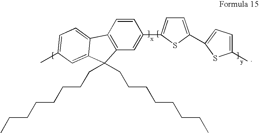
- OFETs were prepared using organic semiconductor of Formula 15.
- a low permittivity perfluoropolymer, Cytop107M (Asahi Glass, Z-1700E01) was used to form the gate insulator.
- the insulator was spin coated from a 1:1 mixture with FC75 solvent (Acros 12380-0100). The devices yielded very low hysteresis and threshold voltage.
- An OFET was prepared using OSC of Formula 15.
- a prior art polar polymer, polymethylmethacrylate (Aldrich 18,226-5) was used to form the gate insulator.
- the insulator was spin coated from a 12.5:1 mixture with acetone. The device exhibited hysteresis and a dependence of the mobility upon applied gate bias.
- An OFET was prepared using an OSC of Formula 14. Three dielectric layers were used to form the gate insulator.
- the first layer (adjacent to the OSC) was a low permittivity perfluoropolymer, Cytop107M (Asahi Glass, Z-1700E01). This was spin coated from a 1:1 mixture with FC75 solvent.
- the second layer polyisobutylene (PIB) (Aldrich, 18,145-5), was spin coated from a 3% (w/w) solution in hexane.
- An OFET was prepared using an OSC of Formula 13 in anisole. Two dielectric layers were used to form the gate insulator. The first layer (adjacent to the OSC) was a low permittivity polymer polyisobutylene (PIB) (Aldrich, 18,145-5), spun from a 3% (w/w) solution in hexane. The second layer, polycyanopulluane (CYMM) (ShinEtsu), was spin coated from a 10% (w/w) solution in acetone. The device yielded very low hysteresis and threshold voltage but achieved a much higher on current than using the PIB alone due to the higher overall capacitance of the PIB/CYMM stack.
- PIB low permittivity polymer polyisobutylene
- CYMM polycyanopulluane
- An OFET was prepared using an OSC of Formula 13. Two dielectric layers were used to form the gate insulator. The first layer (adjacent to the OSC) was a low permittivity polymer polypropylene (Aldrich, 42,818-3) spun from a 1% (w/w) solution in hexane. The second layer, polycyanopulluane (CYMM) (ShinEtsu), was spin coated from a 10% (w/w) solution in acetone.
- CYMM polycyanopulluane
- An OFET was prepared using an OSC of Formula 14. Two dielectric layers were used to form the gate insulator. The first layer (adjacent to the OSC) was a low permittivity perfluoropolymer, Cytop107M (Asahi Glass, Z-1700E01). This was spin coated from a 1% (w/w) solution in FC75 solvent. The sample was subjected to an air plasma for 5 minutes to make the surface more hydrophilic. The second layer, polycyanopulluane (CYMM) (ShinEtsu), was spin coated from a 10% (w/w) solution in acetone. The device yielded very low hysteresis and threshold voltage.
- CYMM polycyanopulluane
- An OFET was prepared using an OSC of Formula 14. Three dielectric layers were used to form the gate insulator.
- the first layer (adjacent to the OSC) was a low permittivity perfluoropolymer, Cytop107M (Asahi Glass, Z-1700E01). This was spin coated from a 1:1 mixture with FC75 solvent.
- the second layer polypropylene (PP) (Aldrich, 42,818-3), was spin coated from a saturated solution in toluene.
- the third layer, poly vinylidine fluoride (PVDF) (Aldrich 42,715-2), was spin coated from a 5% (w/w) solution in NMP (N-Methylpyrrolidone). The device yielded very low hysteresis and threshold voltage.
- An OFET was prepared using an OSC of Formula 14. Three dielectric layers were used to form the gate insulator.
- the first layer (adjacent to the OSC) was a low permittivity perfluoropolymer, Teflon AF1600 (Aldrich, 46,961-0). This was spin coated from a 3% (w/w) solution in FC75 solvent.
- the second layer polypropylene (PP) (Aldrich, 42,818-3), was spin coated from a saturated solution in toluene.
- the third layer, poly vinylidine fluoride (PVDF) (Aldrich 42,715-2), was spin coated from a 5% (w/w) solution in NMP. The device yielded very low hysteresis and threshold voltage.
- the graph shown in FIG. 3 shows the mobility dependence upon the dielectric permittivity. This highlights our preference for choosing dielectrics with a permittivity of between 1.1 and 3.0 for the insulator next to the semiconductor.
- FIG. 5 illustrates the mobility calculated from the transfer curve of FIG. 4 according to Equation 2. This mobility calculation is accurate when Vg is much greater than Vd. It can be seen that for this condition the mobility is fairly independent of the gate voltages.
Abstract
Description
| TABLE 1 | |
| Typical low frequency | |
| Insulator | permittivity (ε) |
| Fluorinated para-xylene | 2.4 |
| Fluoropolyarylether | 2.6 |
| Fluorinated polyimide | 2.7 |
| Polystyrene | 2.5 |
| Poly (α-methyl styrene) | 2.6 |
| Poly (α-vinylnaphtalene) | 2.6 |
| Poly (vinyltoluene) | 2.6 |
| Polyethylene | 2.2–2.3 |
| cis-polybutadiene | 2.0 |
| Polypropylene | 2.2 |
| Polyisoprene | 2.3 |
| Poly (4-methyl-1-pentene) | 2.1 |
| Poly (tetrafluoroethylene) | 2.1 |
| Poly (chorotrifluoroethylene) | 2.3–2.8 |
| Poly (2-methyl-1, 3-butadiene) | 2.4 |
| Poly (p-xylylene) | 2.6 |
| Poly (α-α-α′-α′ tetrafluoro-p-xylylene) | 2.4 |
| Poly [1,1-(2-methyl propane) bis (4-phenyl) | 2.3 |
| carbonate] | |
| Poly (cyclohexyl methacrylate) | 2.5 |
| Poly (chlorostyrene) | 2.6 |
| Poly (2,6-dimethyl-1,4-phenylene ether) | 2.6 |
| Polyisobutylene | 2.2 |
| Poly (vinyl cyclohexane) | 2.2 |
| Poly(arylene ether) | 2.6–2.8 |
| Polyphenylene | 2.6–2.7 |
The above list is non-exhaustive and other polymers could be used, including, for example, poly(4-methylstyrene), poly(1,3-butadiene) or polyphenylene. Copolymers containing the repeat units of the above polymers are also suitable. Copolymers offer the possibility of improving solubility, and continuity of the insulator layer.
| TABLE 2 | |
| Typical low frequency | |
| Insulator | permittivity (ε) |
| Poly (ethylene/tetrafluoroethylene) | 2.6 |
| Poly (ethylene/chlorotrifluoroethylene) | 2.3 |
| Fluorinated ethylene/ |
2–2.5 |
| Polystyrene-co-α-methyl styrene | 2.5–2.6 |
| Ethylene/ethyl acrylate copolymer | 2.8 |
| Poly (styrene/10% butadiene) | 2.6 |
| Poly (styrene/15% butadiene) | 2.6 |
| Poly (styrene/2,4 dimethylstyrene) | 2.5 |
| Cytop | 2.0 |
| Teflon AF | 1.9–2.1 |
| Polypropylene-co-1-butene | 2.2 |
- conjugated hydrocarbon polymers such as polyacene, polyphenylene, poly(phenylene vinylene), polyfluorene including oligomers of those conjugated hydrocarbon polymers; condensed aromatic hydrocarbons such as anthracene, tetracene, chrysene, pentacene, pyrene, perylene, coronene; oligomeric para substituted phenylenes such as p-quaterphenyl (p-4P), p-quinquephenyl (p-5P), p-sexiphenyl (p-6P); conjugated heterocyclic polymers such as poly(3-substituted thiophene), poly(3,4-bisubstituted thiophene), polybenzothiophene, polyisothianapthene, poly(N-substituted pyrrole), poly(3-substituted pyrrole), poly(3,4-bisubstituted pyrrole), polyfuran, polypyridine, poly-1,3,4-oxadiazoles, polyisothianaphthene, poly(N-substituted aniline), poly(2-substituted aniline), poly(3-substituted aniline), poly(2,3-bisubstituted aniline), polyazulene, polypyrene; pyrazoline compounds; polyselenophene; polybenzofuran; polyindole; polypyridazine; benzidine compounds; stilbene compounds; triazines; substituted metallo- or metal-free porphines, phthalocyanines, fluorophthalocyanines, naphthalocyanines or fluoronaphthalocyanines; C60 and C70 fullerenes; N,N′-dialkyl, substituted dialkyl, diaryl or substituted diaryl-1,4,5,8-naphthalenetetracarboxylic diimide and fluoro derivatives; N,N′-dialkyl, substituted dialkyl, diaryl or substituted diaryl 3,4,9,10-perylenetetracarboxylicdiimide; bathophenanthroline; diphenoquinones; 1,3,4-oxadiazoles; 11,11,12,12-tetracyanonaptho-2,6-quinodimethane; α,α′-bis(dithieno[3,2-b2′,3′-d]thiophene); 2,8-dialkyl, substituted dialkyl, diaryl or substituted diaryl anthradithiophene; 2,2′-bibenzo[1,2-b:4,5-b′]dithiophene. Preferred compounds are those from the above list and derivatives thereof which are soluble.

where each Y1 is independently selected from P, S, As, N and Se and preferably polyarylamines, where Y1 is N; Ar1 and Ar2 are aromatic groups and Ar3 is present only if Y1 is N, P, or As in which case it too is an aromatic group. Ar1, Ar2 and Ar3 may be the same or different and represent, independently if in different repeat units, a multivalent (preferably bivalent) aromatic group (preferably mononuclear but optionally polynuclear) optionally substituted by at least one optionally substituted C1-40 carbyl-derived groups and/or at least one other optional substituent, and Ar3 represents, independently if in different repeat units, a mono or multivalent (preferably bivalent) aromatic group (preferably mononuclear but optionally polynuclear) optionally substituted by at least one: optionally substituted C1-40 carbyl-derived group and/or at least one other optional substituent; where at least one terminal group is attached in the polymer to the Ar1, Ar2 and optionally Ar3 groups located at the end of the polymer chains, so as to cap the polymer chains and prevent further polymer growth, and at least one terminal group is derived from at least one end capping reagent used in the polymerisation to form said polymeric material to control the molecular weight thereof.


in which X may be Se, Te or preferably O, S, or —N(R)— where R represents H, optionally substituted alkyl or optionally substituted aryl; R1, R2, A1 and A2 may be independently H, alkyl, alkoxy, thioalkyl, acyl, aryl or substituted aryl, a fluorine atom, a cyano group, a nitro group or an optionally substituted secondary or tertiary alkylamine or arylamine —N(R3)(R4), where R3 and R4 are as defined above. The alkyl and aryl groups represented by R1, R2, R3, R4, A1 and A2 may be optionally fluorinated. The number of recurring units in the conjugated oligomer of Formula 2 is represented by an integer n, n is defined as for Formula 1. In compounds of Formula 2 n is preferably 2 to 14. Preferred oligomers have X=S, R1 and R2=H and A1 and A2=optionally substituted C1-12 alkyl groups, examples of especially preferred compounds being A1 and A2=n-hexyl and where n=4, alpha-omega-n-hexylquaterthienylene (alpha-omega 4T), n=5, alpha-omega-n-hexylpentathienylene (alpha-omega-5T), n=6, alpha-omega-n-hexylhexathienylene (alpha-omega-6T), n=7, alpha-omega-n-hexylheptathienylene (alpha-omega-7T), n=8, alpha-omega-n-hexyloctathienylene (alpha-omega-8T), and n=9, alpha-omega-n-hexylnonathienylene (alpha-omega-9T). Oligomers containing a conjugated linking group may be represented by Formula 3:

in which X may be Se, Te, or preferably O, S, or —N(R)—, R is as defined above; R1, R2, A1 and A2 as defined above for

in which X, R1 and R2 are defined as above. The sub units may be polymerised in such a way as to give a regio regular or a regio random polymer comprising repeat units as shown in Formulae 4 to 6:

Polymers may have repeat units of the general Formula 7:

in which X is as defined above and the bridging group A is optionally fluorinated C1-6 alkyl, for example poly(3,4-ethylenedioxy)thiophene-2,5-diyl and poly(3,4-trimethyldioxy) thiophene-2,5-diyl.

in which X, R1 and R2 are defined as above. Specific examples are where one of R1 or R2 is an alkoxide of general formula CnH2n+1O—, and the other of R1 or R2 is H, poly(dodecyloxy-α,α′,-α,α″ terthienyl) i.e. polyDOT3.

in which X is as defined above; R5 and R6 may be independently H, alkyl, aryl or substituted aryl. The alkyl and aryl groups may be optionally fluorinated.

in which R7 and R8 are each independently optionally substituted C1-20 hydrocarbyl, C4-16 hydrocarbyl carbonyloxy, C4-16 aryl(trialkylsiloxy) or both R7 and R8 may form with the 9-carbon on the fluorene ring a C5-20 ring structure or a C4-20 ring structure containing one or more heteroatoms of S, N or O.

wherein R9 is C1-20 hydrocarbyl optionally substituted with di(C1-10alkyl)amino, C1-20 hydrocarbyloxy or C1-20 hydrocarbyl or tri(C1-10alkyl)siloxy.

This material was prepared using the procedure described in PCT/GB01/05145 to yield a yellow powder (7.8 g). Mw=3700.


This material was prepared using the procedure described in PCT/GB01/05145 to yield an orange solid Mw=17300.
Determination of the Field Effect Mobility
where V0 is an offset voltage and IΩ is an ohmic current independent of the gate voltage and is due to the finite conductivity of the material. The other parameters have been described above.
| TABLE 1 |
| Summary of FET devices prepared using single-layer insulators: |
| Permittivity, ε, | Mobility | |||
| Example | OSC | Insulator layer | of Insulator | [cm2V−1s−1] |
| 5 | 12 | Cytop107M | 2.0 | 2.0 × 10⁻³ |
| 6 | 13 | Cytop107M | 2.0 | 4.0 × 10⁻³ |
| 7 | 13 | Teflon AF1600 | 1.9–2.1 | 2.2 × 10⁻³ |
| 8 | 14 | Cytop107M | 2.0 | 2.0 × 10⁻³ |
| 9 (Comparative) | 14 | PMMA | 4.0 | 4.0 × 10⁻⁴ |
| 10 (Comparative) | 14 | PVP | 3.5 | 5.2 × 10⁻⁴ |
| 11 (Comparative) | 14 | SiO2 | 3.9 | 3.5 × 10⁻⁴ |
| 12 | 13 | Cytop107M | 2.0 | 6.3 × 10⁻³ |
| 13 (Comparative) | 14 | CYMM (2000 nm) | 18.5 | 6.4 × 10⁻⁴ |
| 14 (Comparative) | 14 | CYMM | 18.5 | 4.1 × 10⁻⁴ |
| (2000 nm) | ||||
| 15 | 14 | PIB | 2.2 | 2.6 × 10⁻³ |
| 16 | 13 | PIB | 2.2 | 6.1 × 10⁻³ |
| 17 | 14 | PIBMMA | 2.68 | 1.6 × 10⁻³ |
| 18 (Comparative) | 14 | PVPMMA | ~3.5–4 | 4.6 × 10⁻⁴ |
| 19 | 14 | Teflon AF 2400 | 1.9–2.1 | 1.4 × 10⁻³ |
| 20 (Comparative) | 14 | PVC | 3.1 | 1.2 × 10⁻³ |
| 21 | 14 in binder | Cytop 809A | 2.0 | 8 × 10⁻⁴ |
| 22 (Comparative) | 14 in binder | SiO2 (200 nm) | 3.9 | 1.1 × 10⁻⁴ |
| 23 | 14 | Cytonix PFC2050 | 2.25 | 9.7 × 10⁻⁴ |
| 24 (Comparative) | 14 | PVA | 10.4 | 8.0 × 10⁻⁵ |
| 25 | 14 | PP-co-butene | 2.2 | 1.5 × 10⁻³ |
| 26 | 15 | Cytop107M | 2.0 | 1.7 × 10⁻³ |
| 27 (Comparative) | 15 | PMMA | 4.0 | 3.3 × 10⁻⁴ |
| TABLE 2 |
| Summary of FET devices prepared using multi-layer insulators |
| First insulator | Further insulator | Mobility | ||||
| Example | OSC | layer | ε | layers | ε2, ε3 . . . | [cm2V−1s−1] |
| 28 | 14 | Cytop107M | 2.0 | PIB (350 nm) | 2.1 | 1.4 × 10⁻³ |
| (500 nm) | CYMM (1000 nm) | 18.5 | ||||
| 29 | 13 | PIB (350 nm) | 2.1 | CYMM (2000 nm) | 18.5 | 1.0 × 10⁻² |
| 30 | 13 | PP (27 nm) | CYMM (2000 nm) | 18.5 | 8.6 × 10⁻³ | |
| 31 | 14 | CYTOP 107M | 2.0 | CYMM (2000 nm) | 18.5 | 2.6 × 10⁻³ |
| (200 nm) | ||||||
| 32 | 14 | CYTOP 107M | 2.0 | PP (~30 nm) | 2.2 | 3 × 10⁻³ |
| (500 nm) | PVDF (300 nm) | 7.5 | ||||
| 33 | 14 | TEFLON AF | 19–2.1 | PP (~30 nm) | 2.2 | 1.9 × 10⁻³ |
| 2400 (460 nm) | PVDF (300 nm) | 7.5 | ||||
Claims (35)
Applications Claiming Priority (7)
| Application Number | Priority Date | Filing Date | Title |
|---|---|---|---|
| GB0130321A GB0130321D0 (en) | 2001-12-19 | 2001-12-19 | Electronic devices |
| GB0130321.3 | 2001-12-19 | ||
| GB0130451.8 | 2001-12-20 | ||
| GB0130451A GB0130451D0 (en) | 2001-12-20 | 2001-12-20 | Electronic devices |
| GB0220504A GB0220504D0 (en) | 2002-09-03 | 2002-09-03 | Electronic devices |
| GB0220504.5 | 2002-09-03 | ||
| PCT/GB2002/005248 WO2003052841A1 (en) | 2001-12-19 | 2002-11-21 | Organic field effect transistor with an organic dielectric |
Publications (2)
| Publication Number | Publication Date |
|---|---|
| US20050104058A1 US20050104058A1 (en) | 2005-05-19 |
| US7029945B2 true US7029945B2 (en) | 2006-04-18 |
Family
ID=27256358
Family Applications (1)
| Application Number | Title | Priority Date | Filing Date |
|---|---|---|---|
| US10/499,040 Expired - Lifetime US7029945B2 (en) | 2001-12-19 | 2002-11-21 | Organic field effect transistor with an organic dielectric |
Country Status (9)
| Country | Link |
|---|---|
| US (1) | US7029945B2 (en) |
| EP (3) | EP2207217A1 (en) |
| JP (3) | JP2005513788A (en) |
| KR (1) | KR100949304B1 (en) |
| AT (1) | ATE525757T1 (en) |
| AU (1) | AU2002343058A1 (en) |
| CA (1) | CA2469912A1 (en) |
| NO (1) | NO20043049L (en) |
| WO (1) | WO2003052841A1 (en) |
Cited By (43)
| Publication number | Priority date | Publication date | Assignee | Title |
|---|---|---|---|---|
| US20050230680A1 (en) * | 2004-04-15 | 2005-10-20 | Nec Corporation | Transistor using organic material having a bridged cyclic hydrocarbon lactone structure and process for producing the same |
| US20050263756A1 (en) * | 2004-05-12 | 2005-12-01 | Matsushita Electric Industrial Co., Ltd. | Organic field effect transistor and method of manufacturing the same |
| US20050285112A1 (en) * | 2004-06-29 | 2005-12-29 | Eui-Hoon Hwang | Thin film transistor and method for fabricating the same |
| US20050287697A1 (en) * | 2003-10-09 | 2005-12-29 | Canon Kabushiki Kaisha | Organic semicounductor device, process for producing the same, and organic semiconductor apparatus |
| US20060043432A1 (en) * | 2004-08-31 | 2006-03-02 | Osaka University | Thin-layer chemical transistor and making method |
| US20060049398A1 (en) * | 2004-09-03 | 2006-03-09 | Seiko Epson Corporation | Field-effect transistor comprising a layer of an organic semiconductor |
| US20060186401A1 (en) * | 2004-09-14 | 2006-08-24 | Marks Tobin J | Carbonyl-functionalized thiophene compounds and related device structures |
| US20060202195A1 (en) * | 2004-12-23 | 2006-09-14 | Marks Tobin J | Siloxane-polymer dielectric compositions and related organic field-effect transistors |
| US20060231908A1 (en) * | 2005-04-13 | 2006-10-19 | Xerox Corporation | Multilayer gate dielectric |
| US20070071881A1 (en) * | 2003-08-11 | 2007-03-29 | Lay-Lay Chua | Method of making a polymer device |
| US20070087489A1 (en) * | 2005-10-19 | 2007-04-19 | Samsung Sdi Co., Ltd. | Organic thin film transistor, method of manufacturing the same, and flat panel display comprising the same |
| US20070099333A1 (en) * | 2003-07-17 | 2007-05-03 | Seiko Epson Corporation | Thin-film transistor, method of producing thin-film transistor, electronic circuit, display, and electronic device |
| US20070160847A1 (en) * | 2005-12-21 | 2007-07-12 | Xerox Corporation | Organic thin-film transistors |
| US20070296047A1 (en) * | 2006-06-02 | 2007-12-27 | Air Products And Chemicals, Inc. | Thin film transistors with poly(arylene ether) polymers as gate dielectrics and passivation layers |
| KR100794720B1 (en) | 2006-08-28 | 2008-01-21 | 경희대학교 산학협력단 | Organic thin film transistor array panel and method for manufacturing the same |
| US20080149922A1 (en) * | 2006-12-25 | 2008-06-26 | Industrial Technology Research Institute | Electronic devices with hybrid high-k dielectric and fabrication methods thereof |
| US20080161464A1 (en) * | 2006-06-28 | 2008-07-03 | Marks Tobin J | Crosslinked polymeric dielectric materials and methods of manufacturing and use thereof |
| US20080161524A1 (en) * | 2006-11-28 | 2008-07-03 | He Yan | Photopolymer-based dielectric materials and methods of preparation and use thereof |
| US20090001359A1 (en) * | 2005-12-12 | 2009-01-01 | Polyic Gmbh & Co. Kg | Redox Systems for Stabilization and Life Extension of Polymer Semiconductors |
| US20090020750A1 (en) * | 2005-09-30 | 2009-01-22 | Basf Se | Active semiconductor devices |
| US20090152537A1 (en) * | 2007-12-17 | 2009-06-18 | Electronics And Telecommunications Research Institute | Composition for organic polymer gate insulating layer and organic thin film transistor using the same |
| US20090179194A1 (en) * | 2008-01-16 | 2009-07-16 | Xerox Corporation | Organic thin film transistors |
| US20100044687A1 (en) * | 2006-12-23 | 2010-02-25 | ETH Zürich, ETH Transfer | Organic field-effect transistors with polymeric gate dielectric and method for making same |
| US20100108999A1 (en) * | 2007-04-25 | 2010-05-06 | Merck Patent Gesellschaft Mit Beschrankter Hafting | Process for preparing an electronic device |
| WO2010086651A1 (en) | 2009-01-28 | 2010-08-05 | Nano Eprint Limited | Electronic devices, circuits and their manufacture |
| US20100203663A1 (en) * | 2007-06-22 | 2010-08-12 | Cambridge Display Technology Limited | Organic Thin Film Transistors, Organic Light-emissive Devices and Organic Light-emissive Displays |
| US20100289015A1 (en) * | 2009-05-14 | 2010-11-18 | Commissariat à I'énergie atomique et aux énergies alternatives | Organic field-effect transistor |
| US20110018061A1 (en) * | 2009-07-24 | 2011-01-27 | Electronics And Telecommunications Research Institute | Composition for organic dielectric and organic thin film transistor formed using the same |
| WO2011027159A1 (en) | 2009-09-02 | 2011-03-10 | Nano Eprint Limited | Structures comprising planar electronic devices |
| WO2011072787A1 (en) | 2009-12-17 | 2011-06-23 | Merck Patent Gmbh | Deposition of nanoparticles |
| US20110180784A1 (en) * | 2010-01-22 | 2011-07-28 | Deepak Shukla | Organic semiconducting compositions and n-type semiconductor devices |
| WO2013017170A1 (en) | 2011-08-03 | 2013-02-07 | Universita Degli Studi Di Cagliari | Low voltage organic transistor |
| US20130149812A1 (en) * | 2010-08-18 | 2013-06-13 | Cambridge Display Technology Limited | Low contact resistance organic thin film transistors |
| WO2014008971A1 (en) | 2012-07-13 | 2014-01-16 | Merck Patent Gmbh | Organic electronic device comprising an organic semiconductor formulation |
| WO2014023392A1 (en) | 2012-08-09 | 2014-02-13 | dedeMERCK PATENT GMBH | Organic semiconducting formulation |
| WO2015013396A1 (en) | 2013-07-24 | 2015-01-29 | Orthogonal, Inc. | Cross-linkable fluorinated photopolymer |
| US9175123B2 (en) | 2010-09-02 | 2015-11-03 | Merck Patent Gmbh | Gate insulator layer for organic electronic devices |
| US9330809B2 (en) | 2013-12-17 | 2016-05-03 | Dow Global Technologies Llc | Electrically conducting composites, methods of manufacture thereof and articles comprising the same |
| US9336921B2 (en) | 2013-12-17 | 2016-05-10 | Dow Global Technologies Llc | Electrically conducting composites, methods of manufacture thereof and articles comprising the same |
| US9425417B2 (en) | 2012-09-21 | 2016-08-23 | Merck Patent Gmbh | Polycycloolefinic polymer formulation for an organic semiconductor |
| US9583713B2 (en) | 2010-09-02 | 2017-02-28 | Merck Patent Gmbh | Interlayer for electronic devices |
| US9871215B2 (en) | 2013-11-21 | 2018-01-16 | Nikon Corporation | Transistor manufacturing method and transistor |
| US9958778B2 (en) | 2014-02-07 | 2018-05-01 | Orthogonal, Inc. | Cross-linkable fluorinated photopolymer |
Families Citing this family (132)
| Publication number | Priority date | Publication date | Assignee | Title |
|---|---|---|---|---|
| JP2004241528A (en) * | 2003-02-05 | 2004-08-26 | Ricoh Co Ltd | Organic semiconductor device and display element having it |
| US6950299B2 (en) | 2003-02-13 | 2005-09-27 | Plastic Logic Limited | Non-linear capacitors |
| GB0303267D0 (en) * | 2003-02-13 | 2003-03-19 | Plastic Logic Ltd | Non lineur capacitors |
| KR100726114B1 (en) * | 2003-06-27 | 2007-06-12 | 티디케이가부시기가이샤 | Field effect transistor |
| KR100995451B1 (en) * | 2003-07-03 | 2010-11-18 | 삼성전자주식회사 | Organic Thin Film Transistor comprising Gate Insulator having Multi-layered Structure |
| JP2005072569A (en) * | 2003-08-06 | 2005-03-17 | Mitsubishi Chemicals Corp | Organic fet |
| DE10340608A1 (en) * | 2003-08-29 | 2005-03-24 | Infineon Technologies Ag | Polymer formulation and method of making a dielectric layer |
| JP2005079549A (en) * | 2003-09-03 | 2005-03-24 | Victor Co Of Japan Ltd | Organic thin film transistor |
| US8450723B2 (en) * | 2003-11-04 | 2013-05-28 | Alcatel Lucent | Apparatus having an aromatic dielectric and an aromatic organic semiconductor including an alkyl chain |
| EP1808866A1 (en) | 2003-11-28 | 2007-07-18 | Merck Patent GmbH | Organic semiconducting layer formulations comprising polyacenes and organic binder polymers |
| JP2005175386A (en) * | 2003-12-15 | 2005-06-30 | Asahi Kasei Corp | Organic semiconductor device |
| JP2005191437A (en) * | 2003-12-26 | 2005-07-14 | Ricoh Co Ltd | Semiconductor device, manufacturing method therefor, and display device |
| GB0400997D0 (en) | 2004-01-16 | 2004-02-18 | Univ Cambridge Tech | N-channel transistor |
| US7256436B2 (en) | 2004-03-30 | 2007-08-14 | Shin-Etsu Chemical Co., Ltd. | Thin-film field-effect transistors and making method |
| KR100560796B1 (en) | 2004-06-24 | 2006-03-13 | 삼성에스디아이 주식회사 | organic TFT and fabrication method of the same |
| JP4502382B2 (en) * | 2004-11-02 | 2010-07-14 | キヤノン株式会社 | Organic transistor |
| KR100669752B1 (en) | 2004-11-10 | 2007-01-16 | 삼성에스디아이 주식회사 | Organic thin film transistor, method for manufacturing the same and Flat panel display with the same |
| KR101122231B1 (en) * | 2004-12-17 | 2012-03-19 | 삼성전자주식회사 | Thin film transistor array panel using organic semiconductor and manufacturing method thereof |
| KR101142998B1 (en) | 2004-12-20 | 2012-05-08 | 재단법인서울대학교산학협력재단 | Organic insulator, thin film transistor array panel comprising the organic insulator and manufacturing method thereof |
| KR101086159B1 (en) * | 2005-01-07 | 2011-11-25 | 삼성전자주식회사 | Organic Thin Film Transistor comprising Fluorine-based polymer thin film |
| JP2006229053A (en) * | 2005-02-18 | 2006-08-31 | Ricoh Co Ltd | Field effect organic thin film transistor having organic semiconductor layer |
| CN101120457B (en) | 2005-02-18 | 2011-04-27 | 皇家飞利浦电子股份有限公司 | Electronic device |
| US7619242B2 (en) * | 2005-02-25 | 2009-11-17 | Xerox Corporation | Celluloses and devices thereof |
| JP4450214B2 (en) * | 2005-03-11 | 2010-04-14 | セイコーエプソン株式会社 | Organic thin film transistor, electronic device and electronic equipment |
| JP4951868B2 (en) * | 2005-03-18 | 2012-06-13 | 凸版印刷株式会社 | Thin film transistor manufacturing method |
| JP2006269599A (en) * | 2005-03-23 | 2006-10-05 | Sony Corp | Pattern forming method, method of manufacturing organic field effect transistor, and method of manufacturing flexible printed circuit board |
| ES2450169T3 (en) * | 2005-03-23 | 2014-03-24 | Turkiye Sise Ve Cam Fabrikalari A.S. | Organic field effect transistors based on imide / diimide and a method of production of these |
| US20060214154A1 (en) * | 2005-03-24 | 2006-09-28 | Eastman Kodak Company | Polymeric gate dielectrics for organic thin film transistors and methods of making the same |
| US20060231829A1 (en) * | 2005-04-13 | 2006-10-19 | Xerox Corporation | TFT gate dielectric with crosslinked polymer |
| EP1986247A1 (en) | 2005-05-12 | 2008-10-29 | MERCK PATENT GmbH | Polyacene and semiconductor Formulation |
| TW200703664A (en) * | 2005-05-31 | 2007-01-16 | Nat University Iwate Univ Inc | Organic thin film transistor |
| WO2007010425A1 (en) | 2005-07-19 | 2007-01-25 | Koninklijke Philips Electronics N.V. | Fluid analyser |
| KR101209046B1 (en) * | 2005-07-27 | 2012-12-06 | 삼성디스플레이 주식회사 | Thin film transistor substrate and method of making thin film transistor substrate |
| US7781757B2 (en) | 2005-08-24 | 2010-08-24 | Sanyo Electric Co., Ltd. | Organic semiconductor material, organic semiconductor element and field effect transistor using the same |
| TWI261361B (en) * | 2005-08-31 | 2006-09-01 | Ind Tech Res Inst | Organic thin-film transistor structure and method for fabricating the same is provided |
| US20080113520A1 (en) * | 2005-09-07 | 2008-05-15 | University Of Seoul Foundation Of Industry- Academic Cooperation | Method of Forming Organic Layer on Semiconductor Substrate |
| US7488834B2 (en) | 2005-09-30 | 2009-02-10 | Alcatel-Lucent Usa Inc. | Organic semiconductors |
| US7569415B2 (en) | 2005-09-30 | 2009-08-04 | Alcatel-Lucent Usa Inc. | Liquid phase fabrication of active devices including organic semiconductors |
| CN100511751C (en) * | 2005-10-17 | 2009-07-08 | 中国科学院化学研究所 | An organic field effect transistor and manufacture method thereof |
| KR101213871B1 (en) * | 2005-12-15 | 2012-12-18 | 엘지디스플레이 주식회사 | Thin film transistor array substrate and manufacturing method of the same |
| US7514710B2 (en) * | 2005-12-28 | 2009-04-07 | 3M Innovative Properties Company | Bottom gate thin film transistors |
| KR101225372B1 (en) * | 2005-12-29 | 2013-01-22 | 엘지디스플레이 주식회사 | thin film transistor, fabricating method of the same, and flat panel display having the thin film transistor |
| DE102006055067B4 (en) | 2005-12-29 | 2017-04-20 | Lg Display Co., Ltd. | Organic thin film transistors and process for their manufacture |
| GB2449023B (en) | 2006-01-21 | 2011-06-15 | Merck Patent Gmbh | Electronic short channel device comprising an organic semiconductor formulation |
| JP5062435B2 (en) * | 2006-02-27 | 2012-10-31 | 株式会社村田製作所 | Field effect transistor |
| TW200737520A (en) * | 2006-03-17 | 2007-10-01 | Univ Nat Chiao Tung | Gate dielectric structure and an organic thin film transistor based thereon |
| CN101443928A (en) | 2006-05-12 | 2009-05-27 | 默克专利有限公司 | Indenofluorene polymer based organic semiconductor materials |
| JP2007311377A (en) * | 2006-05-16 | 2007-11-29 | Sony Corp | Manufacturing method of thin-film transistor, thin-film transistor, and display |
| JP5256583B2 (en) * | 2006-05-29 | 2013-08-07 | 大日本印刷株式会社 | Organic semiconductor device and method for manufacturing organic semiconductor device |
| JP2007318025A (en) * | 2006-05-29 | 2007-12-06 | Dainippon Printing Co Ltd | Organic semiconductor element and manufacturing method thereof element |
| US7528448B2 (en) | 2006-07-17 | 2009-05-05 | E.I. Du Pont De Nemours And Company | Thin film transistor comprising novel conductor and dielectric compositions |
| US8308886B2 (en) | 2006-07-17 | 2012-11-13 | E I Du Pont De Nemours And Company | Donor elements and processes for thermal transfer of nanoparticle layers |
| US8062824B2 (en) | 2006-07-17 | 2011-11-22 | E. I. Du Pont De Nemours And Company | Thermally imageable dielectric layers, thermal transfer donors and receivers |
| US8471064B2 (en) | 2006-07-21 | 2013-06-25 | Merck Patent Gmbh | Copolymers of indenofluorene and thiophene |
| WO2008105816A2 (en) * | 2006-08-22 | 2008-09-04 | Northwestern University | Gate dielectric structures, organic semiconductors, thin film transistors and related methods |
| TW200830595A (en) * | 2006-11-27 | 2008-07-16 | Nat University Iwate Univ Inc | Organic thin film transistor, organic composite electronic element, method for manufacturing such transistor and element, and display device and memory |
| JP5234533B2 (en) * | 2007-03-26 | 2013-07-10 | 国立大学法人九州大学 | Organic semiconductor device and manufacturing method thereof |
| GB0709093D0 (en) * | 2007-05-11 | 2007-06-20 | Plastic Logic Ltd | Electronic device incorporating parylene within a dielectric bilayer |
| WO2009013291A2 (en) * | 2007-07-25 | 2009-01-29 | Basf Se | Field effect elements |
| FR2919521B1 (en) | 2007-08-01 | 2012-03-09 | Commissariat Energie Atomique | CONNECTING LAYER ON FLUORINATED POLYMERS |
| TWI345671B (en) * | 2007-08-10 | 2011-07-21 | Au Optronics Corp | Thin film transistor, pixel structure and liquid crystal display panel |
| JP2009224689A (en) * | 2008-03-18 | 2009-10-01 | Sanyo Electric Co Ltd | Organic transistor, and manufacturing method thereof |
| PT103999B (en) * | 2008-03-20 | 2012-11-16 | Univ Nova De Lisboa | METHOD FOR USING AND CREATING PAPER BASED ON NATURAL CELLULOSE FIBERS, SYNTHETIC OR MIST FIBERS AS A PHYSICAL SUPPORT AND HANDLING OF ELECTRICAL LOADS IN SELF-SUSTAINABLE MEMORY FIELD EFFECT TRANSI- TERS USING SEM |
| GB2458940B (en) * | 2008-04-03 | 2010-10-06 | Cambridge Display Tech Ltd | Organic thin film transistors |
| WO2009129912A1 (en) * | 2008-04-24 | 2009-10-29 | Merck Patent Gmbh | Electronic device |
| FR2934714B1 (en) * | 2008-07-31 | 2010-12-17 | Commissariat Energie Atomique | ORGANIC TRANSISTOR AND METHOD FOR MANUFACTURING DIELECTRIC LAYER OF SUCH TRANSISTOR. |
| EP2315793B1 (en) | 2008-08-18 | 2013-08-21 | Merck Patent GmbH | Indacenodithiophene and indacenodiselenophene polymers and their use as organic semiconductors |
| JP2010062276A (en) * | 2008-09-03 | 2010-03-18 | Brother Ind Ltd | Oxide thin-film transistor and method of manufacturing the same |
| DE112009001784T5 (en) | 2008-09-19 | 2011-07-28 | Merck Patent GmbH, 64293 | Benzo-bis (silo-thiophene) derived polymers and their use as organic semiconductors |
| GB2475667B (en) | 2008-09-19 | 2012-08-08 | Merck Patent Gmbh | Polymers derived from bis (thienocyclopenta) benzothiadiazole and their use as organic semiconductors |
| JP2010093093A (en) * | 2008-10-09 | 2010-04-22 | Hitachi Ltd | Semiconductor device and method of manufacturing the same |
| JP5449736B2 (en) * | 2008-10-09 | 2014-03-19 | 株式会社日立製作所 | Bottom gate type organic thin film transistor and manufacturing method thereof |
| KR100975913B1 (en) * | 2008-10-31 | 2010-08-13 | 한국전자통신연구원 | Composition for organic thin film transistor, organic thin film transistor formed by using the same, and method of forming the organic thin film transistor |
| EP3456756A3 (en) | 2008-10-31 | 2019-05-01 | Basf Se | Diketopyrrolopyrrole polymers for use in organic field effect transistors |
| JP2010163521A (en) * | 2009-01-14 | 2010-07-29 | Sumitomo Chemical Co Ltd | Resin composition for insulating layer |
| CN102804439B (en) | 2009-05-25 | 2015-05-27 | 巴斯夫欧洲公司 | Crosslinkable dielectrics and methods of preparation and use thereof |
| EP2435497B1 (en) * | 2009-05-27 | 2023-07-05 | CLAP Co., Ltd. | Polycyclic dithiophenes |
| US8629238B2 (en) | 2009-05-27 | 2014-01-14 | Basf Se | Diketopyrrolopyrrole polymers for use in organic semiconductor devices |
| JP5458669B2 (en) * | 2009-05-28 | 2014-04-02 | ソニー株式会社 | THIN FILM TRANSISTOR, METHOD FOR PRODUCING THIN FILM TRANSISTOR, DISPLAY DEVICE, AND ELECTRONIC DEVICE |
| GB2474827A (en) | 2009-08-04 | 2011-05-04 | Cambridge Display Tech Ltd | Surface modification |
| TWI384616B (en) * | 2009-09-11 | 2013-02-01 | Univ Nat Cheng Kung | Memory device with organic thin-film transistor (otft) structure |
| US8164089B2 (en) | 2009-10-08 | 2012-04-24 | Xerox Corporation | Electronic device |
| JP2011187626A (en) * | 2010-03-08 | 2011-09-22 | Sony Corp | Thin film transistor and electronic apparatus |
| JP5605610B2 (en) * | 2010-04-23 | 2014-10-15 | セイコーエプソン株式会社 | Manufacturing method of organic transistor |
| JP2013533895A (en) | 2010-05-19 | 2013-08-29 | ビーエーエスエフ ソシエタス・ヨーロピア | Diketopyrrolopyrrole-based polymers for use in organic semiconductor devices |
| JP5659568B2 (en) * | 2010-06-11 | 2015-01-28 | 富士ゼロックス株式会社 | Field effect organic transistor |
| WO2011158929A1 (en) * | 2010-06-17 | 2011-12-22 | 住友化学株式会社 | Optical energy-crosslinkable insulating layer material for organic thin film transistor, overcoat insulating layer, and organic thin film transistor |
| CN102959753B (en) | 2010-06-24 | 2017-10-31 | 巴斯夫欧洲公司 | With improving ON/OFF electric current than the organic field effect tube that is moved with controllable threshold |
| CN103003972A (en) | 2010-07-30 | 2013-03-27 | 巴斯夫欧洲公司 | Amphiphilic protein in printed electronics |
| WO2012017005A2 (en) | 2010-08-05 | 2012-02-09 | Basf Se | Polymers based on benzodiones |
| WO2012029700A1 (en) * | 2010-08-30 | 2012-03-08 | 住友化学株式会社 | Composition for insulating layer of organic thin-film transistor, and organic thin-film transistor |
| JP5913107B2 (en) * | 2010-09-07 | 2016-04-27 | 日本化薬株式会社 | Organic semiconductor material, organic semiconductor composition, organic thin film, field effect transistor, and manufacturing method thereof |
| KR20130129926A (en) * | 2010-10-07 | 2013-11-29 | 조지아 테크 리서치 코포레이션 | Field-effect transistor and manufacturing process thereof |
| GB201105482D0 (en) | 2011-03-31 | 2011-05-18 | Imp Innovations Ltd | Polymers |
| GB201108865D0 (en) | 2011-05-26 | 2011-07-06 | Ct For Process Innovation The Ltd | Semiconductor compounds |
| GB201108864D0 (en) | 2011-05-26 | 2011-07-06 | Ct For Process Innovation The Ltd | Transistors and methods of making them |
| FR2980040B1 (en) * | 2011-09-14 | 2016-02-05 | Commissariat Energie Atomique | ORGANIC FIELD EFFECT TRANSISTOR |
| FR2980041B1 (en) * | 2011-09-14 | 2016-02-05 | Commissariat Energie Atomique | FIELD EFFECT TRANSISTOR COMPRISING A LEAKAGE CURRENT LIMITER |
| KR102030860B1 (en) | 2011-10-04 | 2019-11-08 | 바스프 에스이 | Polymers based on benzodiones |
| WO2013072853A1 (en) | 2011-11-15 | 2013-05-23 | Basf Se | Organic semiconductor device and manufacturing method thereof |
| EP2789024B1 (en) | 2011-12-07 | 2015-11-18 | Basf Se | Diketopyrrolopyrrole polymers for use in organic semiconductor devices |
| US9978943B2 (en) | 2011-12-07 | 2018-05-22 | Basf Se | Organic field effect transistor |
| PL397479A1 (en) | 2011-12-21 | 2013-06-24 | Instytut Chemii Organicznej Polskiej Akademii Nauk | New, fluorescent heterocyclic dyes and a process for their manufacturing |
| EP2834284B1 (en) | 2012-04-02 | 2017-05-10 | Basf Se | Phenanthro[9,10-b]furan polymers and small molecules for electronic applications |
| CN103367458B (en) * | 2012-04-03 | 2017-03-01 | 元太科技工业股份有限公司 | Thin film transistor and method of manufacturing the same |
| TWI500162B (en) * | 2012-04-03 | 2015-09-11 | E Ink Holdings Inc | Thin film transistor and manufacturing method thereof |
| CN104334610A (en) | 2012-04-04 | 2015-02-04 | 巴斯夫欧洲公司 | Diketopyrrolopyrrole polymers and small molecules |
| CN104245783B (en) | 2012-04-25 | 2017-12-12 | 默克专利股份有限公司 | Bank structure for organic electronic device |
| KR20150036641A (en) | 2012-07-23 | 2015-04-07 | 바스프 에스이 | Dithienobenzofuran polymers and small molecules for electronic application |
| SG11201501508UA (en) * | 2012-08-31 | 2015-04-29 | Asahi Glass Co Ltd | Curable composition and method for producing cured film |
| JP6036064B2 (en) * | 2012-09-13 | 2016-11-30 | 富士ゼロックス株式会社 | Organic semiconductor transistor |
| WO2014053202A1 (en) | 2012-10-04 | 2014-04-10 | Merck Patent Gmbh | Passivation layers for organic electronic devices |
| EP2917304B1 (en) | 2012-11-07 | 2016-10-26 | Basf Se | Polymers based on naphthodiones |
| EP2928940B1 (en) | 2012-12-04 | 2021-03-03 | CLAP Co., Ltd. | Functionalized benzodithiophene polymers for electronic application |
| WO2014180704A1 (en) | 2013-05-06 | 2014-11-13 | Basf Se | Soluble cyclic imides containing polymers as dielectrics in organic electronic applications |
| JP6191235B2 (en) * | 2013-05-20 | 2017-09-06 | 富士電機株式会社 | Organic transistor and manufacturing method thereof |
| EP3013906B1 (en) | 2013-06-24 | 2020-03-25 | Basf Se | Polymers based on fused diketopyrrolopyrroles |
| EP2818493A1 (en) | 2013-06-25 | 2014-12-31 | Basf Se | Near infrared absorbing polymers for electronic applications |
| GB2534600A (en) * | 2015-01-29 | 2016-08-03 | Cambridge Display Tech Ltd | Organic thin film transistors |
| CN108137591B (en) | 2015-10-21 | 2021-06-22 | Clap有限公司 | Polymers and compounds based on dipyrrolo [1,2-b:1',2' -g ] [2,6] naphthyridine-5, 11-dione |
| CN105404046B (en) * | 2015-12-04 | 2018-06-01 | 深圳市华星光电技术有限公司 | The production method of quantum dot color membrane substrates |
| DE102016104254A1 (en) * | 2016-03-09 | 2017-10-26 | Friedrich-Schiller-Universität Jena | Method for producing a semiconductive film and electronic component |
| CN109153772B (en) | 2016-05-25 | 2022-05-03 | Clap有限公司 | Semiconductor device and method for manufacturing the same |
| TW201832012A (en) * | 2017-01-20 | 2018-09-01 | 日商富士軟片股份有限公司 | Protective layer formation composition, laminate, and kit |
| GB201810710D0 (en) * | 2018-06-29 | 2018-08-15 | Smartkem Ltd | Sputter Protective Layer For Organic Electronic Devices |
| CN109088000B (en) * | 2018-08-22 | 2022-04-12 | 宁波石墨烯创新中心有限公司 | Organic thin film transistor and preparation method thereof |
| DE102019200810B4 (en) * | 2019-01-23 | 2023-12-07 | Technische Universität Dresden | ORGANIC THIN FILM TRANSISTOR AND METHOD FOR PRODUCING THE SAME |
| CN114450812A (en) * | 2019-06-24 | 2022-05-06 | 弗莱克英纳宝有限公司 | Modification of stress response and adhesion behavior of dielectrics by tuning mechanical properties |
| GB201919031D0 (en) | 2019-12-20 | 2020-02-05 | Smartkem Ltd | Sputter protective layer for organic electronic devices |
| US20220223808A1 (en) * | 2020-06-03 | 2022-07-14 | Purdue Research Foundation | Polyimide-based transistor devices and methods of fabricating the same |
| CN113299831B (en) * | 2021-05-21 | 2023-03-24 | 西安电子科技大学 | Low-power consumption flexible thin film transistor based on three layers of insulating media and manufacturing method thereof |
| CN113410385A (en) * | 2021-06-15 | 2021-09-17 | 南方科技大学 | Low-voltage floating gate photoelectric memory and preparation method thereof |
Citations (21)
| Publication number | Priority date | Publication date | Assignee | Title |
|---|---|---|---|---|
| US4565860A (en) | 1984-04-09 | 1986-01-21 | Nissan Motor Co., Ltd. | Polymer of triphenylamine |
| DE3610649A1 (en) | 1986-03-29 | 1987-10-01 | Basf Ag | Polymers containing triphenylamine units |
| US5347144A (en) | 1990-07-04 | 1994-09-13 | Centre National De La Recherche Scientifique (Cnrs) | Thin-layer field-effect transistors with MIS structure whose insulator and semiconductor are made of organic materials |
| JPH07221367A (en) | 1994-01-31 | 1995-08-18 | Matsushita Electric Ind Co Ltd | Oriented laminated film, its manufacture, organic electronic element, and its manufacture |
| US5546889A (en) | 1993-10-06 | 1996-08-20 | Matsushita Electric Industrial Co., Ltd. | Method of manufacturing organic oriented film and method of manufacturing electronic device |
| US5612228A (en) | 1996-04-24 | 1997-03-18 | Motorola | Method of making CMOS with organic and inorganic semiconducting region |
| EP0786820A2 (en) | 1996-01-29 | 1997-07-30 | Motorola, Inc. | Organic thin film transistor with enhanced carrier mobility |
| WO1997033193A2 (en) | 1996-02-23 | 1997-09-12 | The Dow Chemical Company | Cross-linkable or chain extendable polyarylpolyamines and films thereof |
| US5879821A (en) | 1997-11-13 | 1999-03-09 | Xerox Corporation | Electroluminescent polymer compositions and processes thereof |
| US5981970A (en) | 1997-03-25 | 1999-11-09 | International Business Machines Corporation | Thin-film field-effect transistor with organic semiconductor requiring low operating voltages |
| WO2000042668A1 (en) | 1999-01-15 | 2000-07-20 | The Dow Chemical Company | Semiconducting polymer field effect transistor |
| US6100954A (en) | 1996-03-26 | 2000-08-08 | Lg Electronics Inc. | Liquid crystal display with planarizing organic gate insulator and organic planarization layer and method for manufacturing |
| WO2000079617A1 (en) | 1999-06-21 | 2000-12-28 | Cambridge University Technical Services Limited | Aligned polymers for an organic tft |
| US6188452B1 (en) | 1996-07-09 | 2001-02-13 | Lg Electronics, Inc | Active matrix liquid crystal display and method of manufacturing same |
| WO2001020691A1 (en) | 1999-09-10 | 2001-03-22 | Koninklijke Philips Electronics N.V. | Conductive structure based on poly-3,4-alkenedioxythiophene (pedot) and polystyrenesulfonic acid (pss) |
| WO2001047043A1 (en) | 1999-12-21 | 2001-06-28 | Plastic Logic Limited | Solution processed devices |
| CN1348222A (en) | 2001-11-09 | 2002-05-08 | 清华大学 | Organic film FET and its manufacture |
| WO2003030278A2 (en) | 2001-10-01 | 2003-04-10 | Koninklijke Philips Electronics N.V. | Composition, method and electronic device |
| WO2003038921A1 (en) | 2001-10-16 | 2003-05-08 | Siemens Aktiengesellschaft | Insulator for an organic electronic component |
| WO2003041185A2 (en) | 2001-11-05 | 2003-05-15 | 3M Innovative Properties Company | Organic thin film transistor with polymeric interface |
| US20040038459A1 (en) * | 2000-11-28 | 2004-02-26 | Brown Beverley Anne | Field effect transistors and materials and methods for their manufacture |
Family Cites Families (16)
| Publication number | Priority date | Publication date | Assignee | Title |
|---|---|---|---|---|
| DE3751502T2 (en) * | 1986-03-11 | 1996-02-15 | Kanegafuchi Chemical Ind | Electrical or electronic device with a thin layer of polyimide. |
| JP2651691B2 (en) * | 1988-03-03 | 1997-09-10 | バンドー化学株式会社 | New aromatic amine compounds |
| JP2533943B2 (en) | 1989-08-01 | 1996-09-11 | キヤノン株式会社 | Manufacturing method of electrophotographic photoreceptor |
| GB9403503D0 (en) | 1994-02-24 | 1994-04-13 | Inmos Ltd | Memory cell |
| JP2725591B2 (en) * | 1994-03-10 | 1998-03-11 | 日本電気株式会社 | Field-effect transistor |
| US5681664A (en) | 1994-08-04 | 1997-10-28 | Toyo Ink Manufacturing Co., Ltd. | Hole-transporting material and use thereof |
| DE19638447B4 (en) | 1995-09-19 | 2005-12-08 | Ricoh Co., Ltd. | Electrophotographic recording material |
| DE69625018T2 (en) | 1995-09-25 | 2003-04-10 | Toyo Ink Mfg Co | Light-emitting substance for organic electroluminescent device, and organic electroluminescent device with this light-emitting substance suitable therefor |
| US5728801A (en) | 1996-08-13 | 1998-03-17 | The Dow Chemical Company | Poly (arylamines) and films thereof |
| JPH10335671A (en) * | 1997-06-02 | 1998-12-18 | Sharp Corp | Driver monolithic driving element |
| WO2000078843A1 (en) | 1997-12-19 | 2000-12-28 | Avecia Limited | Process for the isolation of polymer fractions |
| GB9726810D0 (en) | 1997-12-19 | 1998-02-18 | Zeneca Ltd | Compounds composition & use |
| US6207472B1 (en) | 1999-03-09 | 2001-03-27 | International Business Machines Corporation | Low temperature thin film transistor fabrication |
| JP2000275678A (en) * | 1999-03-26 | 2000-10-06 | Matsushita Electric Ind Co Ltd | Thin-film semiconductor device and its production |
| JP2001094107A (en) * | 1999-09-20 | 2001-04-06 | Hitachi Ltd | Organic semiconductor device and liquid crystal display device |
| US6912473B2 (en) * | 2002-06-28 | 2005-06-28 | International Business Machines Corporation | Method for verifying cross-sections |
-
2002
- 2002-11-21 JP JP2003553638A patent/JP2005513788A/en active Pending
- 2002-11-21 CA CA002469912A patent/CA2469912A1/en not_active Abandoned
- 2002-11-21 AT AT02779719T patent/ATE525757T1/en not_active IP Right Cessation
- 2002-11-21 EP EP10004332A patent/EP2207217A1/en not_active Withdrawn
- 2002-11-21 US US10/499,040 patent/US7029945B2/en not_active Expired - Lifetime
- 2002-11-21 KR KR1020047009392A patent/KR100949304B1/en active IP Right Grant
- 2002-11-21 AU AU2002343058A patent/AU2002343058A1/en not_active Abandoned
- 2002-11-21 EP EP02779719A patent/EP1459392B1/en not_active Expired - Lifetime
- 2002-11-21 EP EP10004331A patent/EP2204861A1/en not_active Withdrawn
- 2002-11-21 WO PCT/GB2002/005248 patent/WO2003052841A1/en active Application Filing
-
2004
- 2004-07-15 NO NO20043049A patent/NO20043049L/en unknown
-
2011
- 2011-05-16 JP JP2011109286A patent/JP5727293B2/en not_active Expired - Lifetime
- 2011-05-16 JP JP2011109287A patent/JP5727294B2/en not_active Expired - Lifetime
Patent Citations (24)
| Publication number | Priority date | Publication date | Assignee | Title |
|---|---|---|---|---|
| US4565860A (en) | 1984-04-09 | 1986-01-21 | Nissan Motor Co., Ltd. | Polymer of triphenylamine |
| DE3610649A1 (en) | 1986-03-29 | 1987-10-01 | Basf Ag | Polymers containing triphenylamine units |
| US5347144A (en) | 1990-07-04 | 1994-09-13 | Centre National De La Recherche Scientifique (Cnrs) | Thin-layer field-effect transistors with MIS structure whose insulator and semiconductor are made of organic materials |
| US5912473A (en) | 1993-10-06 | 1999-06-15 | Matsushita Electric Industrial Co., Ltd. | Method of manufacturing organic oriented film and method of manufacturing electronic device |
| US5546889A (en) | 1993-10-06 | 1996-08-20 | Matsushita Electric Industrial Co., Ltd. | Method of manufacturing organic oriented film and method of manufacturing electronic device |
| US5556706A (en) | 1993-10-06 | 1996-09-17 | Matsushita Electric Industrial Co., Ltd. | Conductive layered product and method of manufacturing the same |
| JPH07221367A (en) | 1994-01-31 | 1995-08-18 | Matsushita Electric Ind Co Ltd | Oriented laminated film, its manufacture, organic electronic element, and its manufacture |
| EP0786820A2 (en) | 1996-01-29 | 1997-07-30 | Motorola, Inc. | Organic thin film transistor with enhanced carrier mobility |
| WO1997033193A2 (en) | 1996-02-23 | 1997-09-12 | The Dow Chemical Company | Cross-linkable or chain extendable polyarylpolyamines and films thereof |
| US6100954A (en) | 1996-03-26 | 2000-08-08 | Lg Electronics Inc. | Liquid crystal display with planarizing organic gate insulator and organic planarization layer and method for manufacturing |
| US5612228A (en) | 1996-04-24 | 1997-03-18 | Motorola | Method of making CMOS with organic and inorganic semiconducting region |
| US6188452B1 (en) | 1996-07-09 | 2001-02-13 | Lg Electronics, Inc | Active matrix liquid crystal display and method of manufacturing same |
| US5981970A (en) | 1997-03-25 | 1999-11-09 | International Business Machines Corporation | Thin-film field-effect transistor with organic semiconductor requiring low operating voltages |
| US5879821A (en) | 1997-11-13 | 1999-03-09 | Xerox Corporation | Electroluminescent polymer compositions and processes thereof |
| WO2000042668A1 (en) | 1999-01-15 | 2000-07-20 | The Dow Chemical Company | Semiconducting polymer field effect transistor |
| US6204515B1 (en) | 1999-01-15 | 2001-03-20 | The Dow Chemical Company | Semiconducting polymer field effect transistor |
| WO2000079617A1 (en) | 1999-06-21 | 2000-12-28 | Cambridge University Technical Services Limited | Aligned polymers for an organic tft |
| WO2001020691A1 (en) | 1999-09-10 | 2001-03-22 | Koninklijke Philips Electronics N.V. | Conductive structure based on poly-3,4-alkenedioxythiophene (pedot) and polystyrenesulfonic acid (pss) |
| WO2001047043A1 (en) | 1999-12-21 | 2001-06-28 | Plastic Logic Limited | Solution processed devices |
| US20040038459A1 (en) * | 2000-11-28 | 2004-02-26 | Brown Beverley Anne | Field effect transistors and materials and methods for their manufacture |
| WO2003030278A2 (en) | 2001-10-01 | 2003-04-10 | Koninklijke Philips Electronics N.V. | Composition, method and electronic device |
| WO2003038921A1 (en) | 2001-10-16 | 2003-05-08 | Siemens Aktiengesellschaft | Insulator for an organic electronic component |
| WO2003041185A2 (en) | 2001-11-05 | 2003-05-15 | 3M Innovative Properties Company | Organic thin film transistor with polymeric interface |
| CN1348222A (en) | 2001-11-09 | 2002-05-08 | 清华大学 | Organic film FET and its manufacture |
Non-Patent Citations (12)
| Title |
|---|
| Collet et al., "Low-voltage, 30 nm channel length, organic transistors with a self-assembled monolayer as gate insulating films", Applied Physics Letters, 76(14):1941-1943 (Apr. 3, 2000). |
| Dimitrakopoulos C D et al: "Field-effect transistors comprising molecular beam deposited alpha, omega-di-hexyl-hexathienylene and polymeric insulator" Synthetic Metals, 115 Jan. 1998, Elsevier, Switerland, vol. 92, No. 1, pp. 47-52, XP00149864 ISSN: 0379-6779. |
| Gundlach D J et al: "Improved Organic Thin Film Transistor Performance Using Chemically Modified Gate Dielectrics" XP-001149892. |
| Mitzi D B et al: Organic-inorganic electronic devices based on hybrid perovskites XP-001149874. |
| Redecker et al., "High Mobility Hole Transport Fluorene-Triarylamine Copolymers", Adv. Mater., 11(3):241-246 (1999). |
| Sheraw C D et al: "Spin-on polymer gate dielectric for high performance organic thin film transistors" Flat-Panel Displays and Sensors-Principles, Materials and Processes. Symposium (Material S Research Society Symposium Proceedings vol. 558), Flat-Panel Displays and Sensor-Principles, Materials and Processes, Symposium, San Francisco, CA, USA, 4-9, pp. 403-408, XP001149886 2000, Warrendale, PA, USA, Mater. Res. Soc, USA ISBN: 1-55899-465-3 the whole document. |
| Sheraw et al., "Spin-On Polymer Gate Dieletric for High-Performance Organic Thin Film Transistors", Mat. Res. Soc. Symp. Proc., 558:403-408 (2000). |
| Tanaka et al., "Novel hole-transporting materials based on triphenylamine for organic electroluminescent devices", Chem. Commun., pp. 2175-2176 (1996). |
| Tokito et al., "Thermal stability in oligomeric triphenylamine/tris(8-quinolinolato) aluminum electroluminescent devices", Appl. Phys. Lett., 70(15):1929-1931 (Apr. 14, 1997). |
| Tokito et al., "Thermal stability of electroluminescent devices fabricated using novel charge-transporting materials", Polymers Prep. (Am. Chem. Soc. Div. Polymer Chem.). 38(1):388-389 (1997). |
| Veres J et al: Air stable, amorphous Organic Films and their Applications to Solutions Processable Flexible Electronics, XP-001150353. |
| Wittman et al., "Highly oriented thin films of poly(tetrfluoroethylene) as a substrate for oriented growth of materials", Nature, 352:414-417 (Aug. 1, 1991). |
Cited By (81)
| Publication number | Priority date | Publication date | Assignee | Title |
|---|---|---|---|---|
| US7585697B2 (en) * | 2003-07-17 | 2009-09-08 | Seiko Epson Corporation | Thin-film transistor, method of producing thin-film transistor, electronic circuit, display, and electronic device |
| US20070099333A1 (en) * | 2003-07-17 | 2007-05-03 | Seiko Epson Corporation | Thin-film transistor, method of producing thin-film transistor, electronic circuit, display, and electronic device |
| US7718549B2 (en) * | 2003-08-11 | 2010-05-18 | Cambridge University Technical Services Limited | Method of making a polymer device |
| US20070071881A1 (en) * | 2003-08-11 | 2007-03-29 | Lay-Lay Chua | Method of making a polymer device |
| US20050287697A1 (en) * | 2003-10-09 | 2005-12-29 | Canon Kabushiki Kaisha | Organic semicounductor device, process for producing the same, and organic semiconductor apparatus |
| US7795612B2 (en) | 2003-10-09 | 2010-09-14 | Canon Kabushiki Kaisha | Organic semiconductor device, process for producing the same, and organic semiconductor apparatus |
| US20080105868A1 (en) * | 2003-10-09 | 2008-05-08 | Canon Kabushiki Kaisha | Organic semiconductor device, process for producing the same, and organic semiconductor apparatus |
| US20050230680A1 (en) * | 2004-04-15 | 2005-10-20 | Nec Corporation | Transistor using organic material having a bridged cyclic hydrocarbon lactone structure and process for producing the same |
| US7378683B2 (en) * | 2004-04-15 | 2008-05-27 | Nec Corporation | Transistor using organic material having a bridged cyclic hydrocarbon lactone structure and process for producing the same |
| US7372070B2 (en) * | 2004-05-12 | 2008-05-13 | Matsushita Electric Industrial Co., Ltd. | Organic field effect transistor and method of manufacturing the same |
| US20050263756A1 (en) * | 2004-05-12 | 2005-12-01 | Matsushita Electric Industrial Co., Ltd. | Organic field effect transistor and method of manufacturing the same |
| US20050285112A1 (en) * | 2004-06-29 | 2005-12-29 | Eui-Hoon Hwang | Thin film transistor and method for fabricating the same |
| US7557392B2 (en) * | 2004-08-31 | 2009-07-07 | Osaka University | Field effect transistor and making method |
| US20060043432A1 (en) * | 2004-08-31 | 2006-03-02 | Osaka University | Thin-layer chemical transistor and making method |
| US20060049398A1 (en) * | 2004-09-03 | 2006-03-09 | Seiko Epson Corporation | Field-effect transistor comprising a layer of an organic semiconductor |
| US7579620B2 (en) | 2004-09-03 | 2009-08-25 | Seiko Epson Corporation | Field-effect transistor comprising a layer of an organic semiconductor |
| US20090267061A1 (en) * | 2004-09-14 | 2009-10-29 | Marks Tobin J | Carbonyl-Functionalized Thiophene Compounds and Related Device Structures |
| US7964650B2 (en) | 2004-09-14 | 2011-06-21 | Northwestern University | Carbonyl-functionalized thiophene compounds and related device structures |
| US20060186401A1 (en) * | 2004-09-14 | 2006-08-24 | Marks Tobin J | Carbonyl-functionalized thiophene compounds and related device structures |
| US7528176B2 (en) | 2004-09-14 | 2009-05-05 | Northwestern University | Carbonyl-functionalized thiophene compounds and related device structures |
| US8093588B2 (en) | 2004-12-23 | 2012-01-10 | Northwestern University | Siloxane-polymer dielectric compositions and related organic field-effect transistors |
| US7605394B2 (en) | 2004-12-23 | 2009-10-20 | Northwestern University | Siloxane-polymer dielectric compositions and related organic field-effect transistors |
| US20060202195A1 (en) * | 2004-12-23 | 2006-09-14 | Marks Tobin J | Siloxane-polymer dielectric compositions and related organic field-effect transistors |
| US20060231908A1 (en) * | 2005-04-13 | 2006-10-19 | Xerox Corporation | Multilayer gate dielectric |
| US20090020750A1 (en) * | 2005-09-30 | 2009-01-22 | Basf Se | Active semiconductor devices |
| US7732812B2 (en) | 2005-09-30 | 2010-06-08 | Basf Se | Active semiconductor devices |
| US7800102B2 (en) * | 2005-10-19 | 2010-09-21 | Samsung Mobile Display Co., Ltd. | Organic thin film transistor including a self-assembly monolayer between an insulating layer and an organic semiconductor layer and flat panel display comprising the same |
| US20070087489A1 (en) * | 2005-10-19 | 2007-04-19 | Samsung Sdi Co., Ltd. | Organic thin film transistor, method of manufacturing the same, and flat panel display comprising the same |
| US20090001359A1 (en) * | 2005-12-12 | 2009-01-01 | Polyic Gmbh & Co. Kg | Redox Systems for Stabilization and Life Extension of Polymer Semiconductors |
| US7425723B2 (en) * | 2005-12-21 | 2008-09-16 | Xerox Corporation | Organic thin-film transistors |
| US20070160847A1 (en) * | 2005-12-21 | 2007-07-12 | Xerox Corporation | Organic thin-film transistors |
| US7919825B2 (en) * | 2006-06-02 | 2011-04-05 | Air Products And Chemicals, Inc. | Thin film transistors with poly(arylene ether) polymers as gate dielectrics and passivation layers |
| US20070296047A1 (en) * | 2006-06-02 | 2007-12-27 | Air Products And Chemicals, Inc. | Thin film transistors with poly(arylene ether) polymers as gate dielectrics and passivation layers |
| US20080161464A1 (en) * | 2006-06-28 | 2008-07-03 | Marks Tobin J | Crosslinked polymeric dielectric materials and methods of manufacturing and use thereof |
| US20110024729A1 (en) * | 2006-06-28 | 2011-02-03 | Marks Tobin J | Crosslinked Polymeric Dielectric Materials And Electronic Devices Incorporating Same |
| US8274075B2 (en) | 2006-06-28 | 2012-09-25 | Northwestern University | Crosslinked polymeric dielectric materials and electronic devices incorporating same |
| KR100794720B1 (en) | 2006-08-28 | 2008-01-21 | 경희대학교 산학협력단 | Organic thin film transistor array panel and method for manufacturing the same |
| US8338555B2 (en) | 2006-11-28 | 2012-12-25 | Polyera Corporation | Photopolymers and their use in organic thin film transistors |
| US7981989B2 (en) | 2006-11-28 | 2011-07-19 | Polyera Corporation | Photopolymer-based dielectric materials and methods of preparation and use thereof |
| US20080161524A1 (en) * | 2006-11-28 | 2008-07-03 | He Yan | Photopolymer-based dielectric materials and methods of preparation and use thereof |
| US20100044687A1 (en) * | 2006-12-23 | 2010-02-25 | ETH Zürich, ETH Transfer | Organic field-effect transistors with polymeric gate dielectric and method for making same |
| US20080149922A1 (en) * | 2006-12-25 | 2008-06-26 | Industrial Technology Research Institute | Electronic devices with hybrid high-k dielectric and fabrication methods thereof |
| US7842946B2 (en) * | 2006-12-25 | 2010-11-30 | Industrial Technology Research Institute | Electronic devices with hybrid high-k dielectric and fabrication methods thereof |
| US20090087944A1 (en) * | 2006-12-25 | 2009-04-02 | Industrial Technology Research Institute | Electronic devices with hybrid high-k dielectric and fabrication methods thereof |
| US20100108999A1 (en) * | 2007-04-25 | 2010-05-06 | Merck Patent Gesellschaft Mit Beschrankter Hafting | Process for preparing an electronic device |
| US8637343B2 (en) * | 2007-04-25 | 2014-01-28 | Merck Patent Gmbh | Process for preparing an electronic device |
| US20100203663A1 (en) * | 2007-06-22 | 2010-08-12 | Cambridge Display Technology Limited | Organic Thin Film Transistors, Organic Light-emissive Devices and Organic Light-emissive Displays |
| US8394665B2 (en) * | 2007-06-22 | 2013-03-12 | Cambridge Display Technology Limited | Organic thin film transistors, organic light-emissive devices and organic light-emissive displays |
| US20090152537A1 (en) * | 2007-12-17 | 2009-06-18 | Electronics And Telecommunications Research Institute | Composition for organic polymer gate insulating layer and organic thin film transistor using the same |
| US7741635B2 (en) * | 2007-12-17 | 2010-06-22 | Electronics And Telecommunications Research Institute | Composition for organic polymer gate insulating layer and organic thin film transistor using the same |
| US7994495B2 (en) * | 2008-01-16 | 2011-08-09 | Xerox Corporation | Organic thin film transistors |
| US20090179194A1 (en) * | 2008-01-16 | 2009-07-16 | Xerox Corporation | Organic thin film transistors |
| WO2010086651A1 (en) | 2009-01-28 | 2010-08-05 | Nano Eprint Limited | Electronic devices, circuits and their manufacture |
| US20100289015A1 (en) * | 2009-05-14 | 2010-11-18 | Commissariat à I'énergie atomique et aux énergies alternatives | Organic field-effect transistor |
| FR2945669A1 (en) * | 2009-05-14 | 2010-11-19 | Commissariat Energie Atomique | ORGANIC FIELD EFFECT TRANSISTOR |
| US8314451B2 (en) * | 2009-05-14 | 2012-11-20 | Commissariat à l'énergie atomique et aux énergies alternatives | Organic field-effect transistor |
| US20110018061A1 (en) * | 2009-07-24 | 2011-01-27 | Electronics And Telecommunications Research Institute | Composition for organic dielectric and organic thin film transistor formed using the same |
| US8362467B2 (en) | 2009-07-24 | 2013-01-29 | Electronics And Telecommunications Research Institute | Composition for an organic dielectric |
| WO2011027159A1 (en) | 2009-09-02 | 2011-03-10 | Nano Eprint Limited | Structures comprising planar electronic devices |
| WO2011072787A1 (en) | 2009-12-17 | 2011-06-23 | Merck Patent Gmbh | Deposition of nanoparticles |
| US20110180784A1 (en) * | 2010-01-22 | 2011-07-28 | Deepak Shukla | Organic semiconducting compositions and n-type semiconductor devices |
| US8212243B2 (en) | 2010-01-22 | 2012-07-03 | Eastman Kodak Company | Organic semiconducting compositions and N-type semiconductor devices |
| US20130149812A1 (en) * | 2010-08-18 | 2013-06-13 | Cambridge Display Technology Limited | Low contact resistance organic thin film transistors |
| US9159926B2 (en) * | 2010-08-18 | 2015-10-13 | Cambridge Display Technology Limited | Low contact resistance organic thin film transistors |
| US9583713B2 (en) | 2010-09-02 | 2017-02-28 | Merck Patent Gmbh | Interlayer for electronic devices |
| US9647213B2 (en) | 2010-09-02 | 2017-05-09 | Merck Patent Gmbh | Interlayer for electronic devices |
| US9647222B2 (en) | 2010-09-02 | 2017-05-09 | Merck Patent Gmbh | Gate insulator layer for organic electronic devices |
| US9175123B2 (en) | 2010-09-02 | 2015-11-03 | Merck Patent Gmbh | Gate insulator layer for organic electronic devices |
| WO2013017170A1 (en) | 2011-08-03 | 2013-02-07 | Universita Degli Studi Di Cagliari | Low voltage organic transistor |
| WO2014008971A1 (en) | 2012-07-13 | 2014-01-16 | Merck Patent Gmbh | Organic electronic device comprising an organic semiconductor formulation |
| WO2014023392A1 (en) | 2012-08-09 | 2014-02-13 | dedeMERCK PATENT GMBH | Organic semiconducting formulation |
| US9425417B2 (en) | 2012-09-21 | 2016-08-23 | Merck Patent Gmbh | Polycycloolefinic polymer formulation for an organic semiconductor |
| US9541829B2 (en) | 2013-07-24 | 2017-01-10 | Orthogonal, Inc. | Cross-linkable fluorinated photopolymer |
| WO2015013396A1 (en) | 2013-07-24 | 2015-01-29 | Orthogonal, Inc. | Cross-linkable fluorinated photopolymer |
| US9871215B2 (en) | 2013-11-21 | 2018-01-16 | Nikon Corporation | Transistor manufacturing method and transistor |
| US9336921B2 (en) | 2013-12-17 | 2016-05-10 | Dow Global Technologies Llc | Electrically conducting composites, methods of manufacture thereof and articles comprising the same |
| US9330809B2 (en) | 2013-12-17 | 2016-05-03 | Dow Global Technologies Llc | Electrically conducting composites, methods of manufacture thereof and articles comprising the same |
| US9958778B2 (en) | 2014-02-07 | 2018-05-01 | Orthogonal, Inc. | Cross-linkable fluorinated photopolymer |
| US10289000B2 (en) | 2014-02-07 | 2019-05-14 | Orthogonal, Inc. | Cross-linkable fluorinated photopolymer |
| US10739680B2 (en) | 2014-02-07 | 2020-08-11 | Orthogonal, Inc. | Cross-linkable fluorinated photopolymer |
| US10838302B2 (en) | 2014-02-07 | 2020-11-17 | Orthogonal, Inc. | Cross-linkable fluorinated photopolymer |
Also Published As
| Publication number | Publication date |
|---|---|
| KR20040063176A (en) | 2004-07-12 |
| EP2207217A1 (en) | 2010-07-14 |
| US20050104058A1 (en) | 2005-05-19 |
| EP1459392B1 (en) | 2011-09-21 |
| JP5727293B2 (en) | 2015-06-03 |
| EP2204861A1 (en) | 2010-07-07 |
| AU2002343058A1 (en) | 2003-06-30 |
| KR100949304B1 (en) | 2010-03-23 |
| JP2011254075A (en) | 2011-12-15 |
| ATE525757T1 (en) | 2011-10-15 |
| WO2003052841A1 (en) | 2003-06-26 |
| NO20043049L (en) | 2004-07-15 |
| EP1459392A1 (en) | 2004-09-22 |
| CA2469912A1 (en) | 2003-06-26 |
| JP2011243986A (en) | 2011-12-01 |
| JP5727294B2 (en) | 2015-06-03 |
| JP2005513788A (en) | 2005-05-12 |
Similar Documents
| Publication | Publication Date | Title |
|---|---|---|
| US7029945B2 (en) | Organic field effect transistor with an organic dielectric | |
| US7095044B2 (en) | Field effect transistors and materials and methods for their manufacture | |
| CN1698217B (en) | Organic field effect transistor with an organic dielectric | |
| AU2002220818A1 (en) | Field effect transistors and materials and methods for their manufacture | |
| EP1579518A1 (en) | Improvements in and relating to organic semiconducting materials | |
| TWI644964B (en) | Organic semiconducting formulation | |
| US10164191B2 (en) | Methoxyaryl surface modifier and organic electronic devices comprising such methoxyaryl surface modifier | |
| WO2009016107A1 (en) | Method for depositing a semiconducting layer from a liquid | |
| Pospiech et al. | Self-organizing semifluorinated polymers for organic electronics | |
| KR101702595B1 (en) | Forming Agent for Gate Dielectric of Thin Film Transistor | |
| Ngo | Veres et a1. | |
| US9525135B2 (en) | Thixotropic composition |
Legal Events
| Date | Code | Title | Description |
|---|---|---|---|
| AS | Assignment |
Owner name: AVECIA LIMITED, UNITED KINGDOM Free format text: ASSIGNMENT OF ASSIGNORS INTEREST;ASSIGNORS:VERES, JANOS;OGIER, SIMON DOMINIC;MOHIALDIN-KHAFFAF, SOAD;AND OTHERS;REEL/FRAME:016141/0881;SIGNING DATES FROM 20040513 TO 20040520 |
|
| AS | Assignment |
Owner name: MERCK PATENT GMBH, GERMANY Free format text: ASSIGNMENT OF ASSIGNORS INTEREST;ASSIGNOR:AVECIA LIMITED;REEL/FRAME:017124/0673 Effective date: 20050905 |
|
| STCF | Information on status: patent grant |
Free format text: PATENTED CASE |
|
| FPAY | Fee payment |
Year of fee payment: 4 |
|
| FPAY | Fee payment |
Year of fee payment: 8 |
|
| MAFP | Maintenance fee payment |
Free format text: PAYMENT OF MAINTENANCE FEE, 12TH YEAR, LARGE ENTITY (ORIGINAL EVENT CODE: M1553) Year of fee payment: 12 |