US7033948B2 - Method for reducing dimensions between patterns on a photoresist - Google Patents
Method for reducing dimensions between patterns on a photoresist Download PDFInfo
- Publication number
- US7033948B2 US7033948B2 US10/739,049 US73904903A US7033948B2 US 7033948 B2 US7033948 B2 US 7033948B2 US 73904903 A US73904903 A US 73904903A US 7033948 B2 US7033948 B2 US 7033948B2
- Authority
- US
- United States
- Prior art keywords
- layer
- photoresist
- photoresist structures
- polymer
- over
- Prior art date
- Legal status (The legal status is an assumption and is not a legal conclusion. Google has not performed a legal analysis and makes no representation as to the accuracy of the status listed.)
- Expired - Lifetime
Links
Images


Classifications
-
- H—ELECTRICITY
- H01—ELECTRIC ELEMENTS
- H01L—SEMICONDUCTOR DEVICES NOT COVERED BY CLASS H10
- H01L21/00—Processes or apparatus adapted for the manufacture or treatment of semiconductor or solid state devices or of parts thereof
- H01L21/02—Manufacture or treatment of semiconductor devices or of parts thereof
- H01L21/027—Making masks on semiconductor bodies for further photolithographic processing not provided for in group H01L21/18 or H01L21/34
- H01L21/0271—Making masks on semiconductor bodies for further photolithographic processing not provided for in group H01L21/18 or H01L21/34 comprising organic layers
- H01L21/0273—Making masks on semiconductor bodies for further photolithographic processing not provided for in group H01L21/18 or H01L21/34 comprising organic layers characterised by the treatment of photoresist layers
- H01L21/0274—Photolithographic processes
-
- G—PHYSICS
- G03—PHOTOGRAPHY; CINEMATOGRAPHY; ANALOGOUS TECHNIQUES USING WAVES OTHER THAN OPTICAL WAVES; ELECTROGRAPHY; HOLOGRAPHY
- G03F—PHOTOMECHANICAL PRODUCTION OF TEXTURED OR PATTERNED SURFACES, e.g. FOR PRINTING, FOR PROCESSING OF SEMICONDUCTOR DEVICES; MATERIALS THEREFOR; ORIGINALS THEREFOR; APPARATUS SPECIALLY ADAPTED THEREFOR
- G03F7/00—Photomechanical, e.g. photolithographic, production of textured or patterned surfaces, e.g. printing surfaces; Materials therefor, e.g. comprising photoresists; Apparatus specially adapted therefor
- G03F7/26—Processing photosensitive materials; Apparatus therefor
- G03F7/40—Treatment after imagewise removal, e.g. baking
- G03F7/405—Treatment with inorganic or organometallic reagents after imagewise removal
-
- H—ELECTRICITY
- H01—ELECTRIC ELEMENTS
- H01L—SEMICONDUCTOR DEVICES NOT COVERED BY CLASS H10
- H01L21/00—Processes or apparatus adapted for the manufacture or treatment of semiconductor or solid state devices or of parts thereof
- H01L21/02—Manufacture or treatment of semiconductor devices or of parts thereof
- H01L21/027—Making masks on semiconductor bodies for further photolithographic processing not provided for in group H01L21/18 or H01L21/34
- H01L21/033—Making masks on semiconductor bodies for further photolithographic processing not provided for in group H01L21/18 or H01L21/34 comprising inorganic layers
- H01L21/0332—Making masks on semiconductor bodies for further photolithographic processing not provided for in group H01L21/18 or H01L21/34 comprising inorganic layers characterised by their composition, e.g. multilayer masks, materials
-
- H—ELECTRICITY
- H01—ELECTRIC ELEMENTS
- H01L—SEMICONDUCTOR DEVICES NOT COVERED BY CLASS H10
- H01L21/00—Processes or apparatus adapted for the manufacture or treatment of semiconductor or solid state devices or of parts thereof
- H01L21/02—Manufacture or treatment of semiconductor devices or of parts thereof
- H01L21/027—Making masks on semiconductor bodies for further photolithographic processing not provided for in group H01L21/18 or H01L21/34
- H01L21/033—Making masks on semiconductor bodies for further photolithographic processing not provided for in group H01L21/18 or H01L21/34 comprising inorganic layers
- H01L21/0334—Making masks on semiconductor bodies for further photolithographic processing not provided for in group H01L21/18 or H01L21/34 comprising inorganic layers characterised by their size, orientation, disposition, behaviour, shape, in horizontal or vertical plane
- H01L21/0335—Making masks on semiconductor bodies for further photolithographic processing not provided for in group H01L21/18 or H01L21/34 comprising inorganic layers characterised by their size, orientation, disposition, behaviour, shape, in horizontal or vertical plane characterised by their behaviour during the process, e.g. soluble masks, redeposited masks
-
- H—ELECTRICITY
- H01—ELECTRIC ELEMENTS
- H01L—SEMICONDUCTOR DEVICES NOT COVERED BY CLASS H10
- H01L21/00—Processes or apparatus adapted for the manufacture or treatment of semiconductor or solid state devices or of parts thereof
- H01L21/02—Manufacture or treatment of semiconductor devices or of parts thereof
- H01L21/027—Making masks on semiconductor bodies for further photolithographic processing not provided for in group H01L21/18 or H01L21/34
- H01L21/033—Making masks on semiconductor bodies for further photolithographic processing not provided for in group H01L21/18 or H01L21/34 comprising inorganic layers
- H01L21/0334—Making masks on semiconductor bodies for further photolithographic processing not provided for in group H01L21/18 or H01L21/34 comprising inorganic layers characterised by their size, orientation, disposition, behaviour, shape, in horizontal or vertical plane
- H01L21/0338—Process specially adapted to improve the resolution of the mask
-
- Y—GENERAL TAGGING OF NEW TECHNOLOGICAL DEVELOPMENTS; GENERAL TAGGING OF CROSS-SECTIONAL TECHNOLOGIES SPANNING OVER SEVERAL SECTIONS OF THE IPC; TECHNICAL SUBJECTS COVERED BY FORMER USPC CROSS-REFERENCE ART COLLECTIONS [XRACs] AND DIGESTS
- Y10—TECHNICAL SUBJECTS COVERED BY FORMER USPC
- Y10S—TECHNICAL SUBJECTS COVERED BY FORMER USPC CROSS-REFERENCE ART COLLECTIONS [XRACs] AND DIGESTS
- Y10S438/00—Semiconductor device manufacturing: process
- Y10S438/942—Masking
- Y10S438/947—Subphotolithographic processing
-
- Y—GENERAL TAGGING OF NEW TECHNOLOGICAL DEVELOPMENTS; GENERAL TAGGING OF CROSS-SECTIONAL TECHNOLOGIES SPANNING OVER SEVERAL SECTIONS OF THE IPC; TECHNICAL SUBJECTS COVERED BY FORMER USPC CROSS-REFERENCE ART COLLECTIONS [XRACs] AND DIGESTS
- Y10—TECHNICAL SUBJECTS COVERED BY FORMER USPC
- Y10S—TECHNICAL SUBJECTS COVERED BY FORMER USPC CROSS-REFERENCE ART COLLECTIONS [XRACs] AND DIGESTS
- Y10S438/00—Semiconductor device manufacturing: process
- Y10S438/942—Masking
- Y10S438/948—Radiation resist
- Y10S438/951—Lift-off
Definitions
- This invention relates in general to a semiconductor manufacturing process and, more particularly, to a photolithographic method having reduced dimensions between patterns on a photoresist.
- the resolution of a conventional photolithographic method is primarily dependent upon the wavelength of a light source, which dictates that there be a certain fixed distance between patterns on a photoresist. Distance separating patterns smaller than the wavelength of the light source could not be accurately patterned and defined.
- Prior art light sources with lower wavelengths are normally used in a high-resolution photolithographic process.
- the depth of focus of a high-resolution photolithographic process is shallower compared to a relative low-resolution photolithographic process.
- a photoresist layer having a lower thickness is required for conventional photolithographic methods.
- a photoresist layer having a lower thickness is susceptible to the subsequent etching steps in a semiconductor manufacturing process. This relative ineffective resistance to etching reduces the precision of patterning and defining of a photoresist.
- a semiconductor manufacturing method that includes depositing a layer of semiconductor material over a substrate, providing a layer of photoresist over the layer of semiconductor material, patterning and defining the photoresist layer, depositing a layer of inorganic material over the patterned and defined photoresist layer, wherein the layer of inorganic material is photo-insensitive, anisotropic etching the layer of inorganic material and the layer of semiconductor material, and removing the patterned and defined photoresist layer.
- the layer of inorganic material is substantially conformal.
- the step of depositing a layer of inorganic material is performed at a temperature lower than a stability temperature of the patterned and defined photoresist layer.
- a semiconductor manufacturing method that includes defining a substrate, depositing a layer of semiconductor material over the substrate, providing a layer of photoresist over the layer of semiconductor material, patterning and defining the photoresist layer to form at least one photoresist structure having at least one substantially vertical sidewall and one substantially horizontal top, depositing a photo-insensitive material over the at least one photoresist structure and the layer of semiconductor material, wherein an amount of the photo-insensitive material deposited on the top of the photoresist structure is substantially greater than an amount of the photo-insensitive material deposited on the at least one sidewall of the photoresist structure, etching the photo-insensitive material and the layer of semiconductor material, and removing the at least one photoresist structure.
- the amount of the photo-insensitive material deposited on the top of the photoresist structure is substantially greater than an amount of the photo-insensitive material deposited on the layer of semiconductor material.
- a semiconductor manufacturing method that includes defining a substrate, providing a first layer over the substrate, providing a layer of photoresist over the first layer, patterning and defining the photoresist layer to form at least two photoresist structures, wherein each of the photoresist structures includes substantially vertical sidewalls and a substantially horizontal top, and wherein the photoresist structures are separated by a space, depositing a layer of polymer on the tops of the photoresist structures and the space separating the photoresist structures, wherein an amount of the polymer deposited on the tops of the photoresist structures is substantially greater than an amount of the polymer deposited on the sidewalls of the photoresist structures, and etching the polymer layer on the tops of the photoresist structures and the space between the photoresist structures, and the first layer.
- the first layer is a dielectric layer.
- FIGS. 1–3 are cross-sectional views of the semiconductor manufacturing process steps of the present invention.
- FIGS. 1–3 are cross-sectional views of the semiconductor manufacturing process steps of the present invention.
- the method of the present invention begins by defining a wafer substrate 100 .
- the wafer substrate 100 may be of any known semiconductor substrate material, such as silicon.
- a first layer 110 is then provided over the wafer substrate 100 .
- the first layer 110 is a semiconductor material, such as polysilicon.
- the first layer 110 may also be a dielectric layer or a metal layer.
- the first layer 110 may be deposited over the wafer substrate 100 by any known deposition process.
- the first layer 110 is a dielectric material, in which case the first layer 110 may be deposited or grown over the wafer substrate 100 .
- An anti-reflection coating (ARC) layer 120 may optionally be provided over the first layer 110 to decrease the reflection from the first layer 110 in the subsequent manufacturing steps.
- a photoresist layer 130 is then provided over the ARC layer 120 .
- the photoresist layer 130 is deposited over the first layer 110 .
- the photoresist layer 130 is then patterned and defined using a known photolithographic process to form a patterned and defined photoresist layer having a plurality of photoresist structures 130 .
- the photoresist structures 130 include substantially vertical sidewalls 132 and substantially horizontal tops 134 .
- the photoresist structures 130 functions to form conductors from the first layer 110 .
- a second layer 150 is deposited over the patterned and defined photoresist layer 130 by a known chemical vapor deposition apparatus 140 .
- Known chemical vapor deposition processes include plasma enhanced chemical vapor deposition (PECVD) and low pressure chemical vapor deposition (LPCVD).
- PECVD plasma enhanced chemical vapor deposition
- LPCVD low pressure chemical vapor deposition
- the second layer 150 may be organic or inorganic, and is photo-insensitive.
- the second layer 150 is a polymer layer.
- the second layer 150 is substantially conformal, covering both the tops 134 and sidewalls 132 of the photoresist structures 130 .
- the amount of the second layer 150 deposited on the tops 134 of the photoresist structures 130 is substantially greater than the amount adhered to the sidewalls 132 .
- the photoresist structures 130 become more resistive to the subsequent etching steps, thereby preserving the precision of the photolithographic process.
- the step of depositing the second layer 150 is performed at a temperature lower than the stability temperature of the photoresist structures 130 . In other words, the second layer 150 is deposited at a temperature not affecting the structural stability of the photoresist structures 130 .
- the space between the photoresist structures 130 is decreased, for example, from 0.22 microns to 0.02 microns.
- the pressure used is in the range of approximately 10 mTorr to 20 mTorr.
- the power ranges from approximately 500 watts to 800 watts.
- the deposition rate is between approximately 3,000 ⁇ per minute and 6,000 ⁇ per minute.
- the polymer layer 150 comprises at least one hydrocarbon partially substituted by fluorine, the source for forming polymers.
- the partially-substituted hydrocarbons may be chosen from difluoromethane (CH 2 F 2 ), a mixture of difluoromethane and octafluorobutene (C 4 F 8 ), and a mixture of difluoromethane and trifluoromethane (CHF 3 ).
- the thickness “a” of a portion of the polymer layer 150 is the same as the thickness “b” of another portion of the polymer layer 150 .
- the thickness “a” is larger than the thickness “b.” Therefore, the thicknesses “a” and “b” may be varied by adjusting the ratios of CH 2 F 2 to C 4 F 8 or those of CH 2 F 2 to CHF 3 .
- argon (Ar) and carbon monoxide (CO) may be mixed with the gases introduced during the PECVD process.
- Argon acts as a carrier to enhance etch uniformity of the photoresist layer 130 and the ARC layer 120 .
- the function of carbon monoxide is to capture fluorine radicals and fluoride ions generated by the fluoro-substituted hydrocarbons. As such, etching of the polymers during the deposition process is prevented, thereby enhancing the deposition rate of the polymer layer 150 .
- Oxygen (O 2 ) and nitrogen (N 2 ) gases also can be added to the PECVD process. Contrary to the function of the carbon monoxide, the presence of oxygen serves to etch the polymer layer 150 .
- the deposition rate of polymer layer 150 can be controlled.
- perfluorohydrocarbons such as hexafluoroethane (C 2 F 6 ) and tetrafluoromethane (CF 4 ) can be mixed with the gases combined with the plasma during the deposition because these gases, similar to the oxygen gas, etch the polymer layer 150 .
- the second layer 150 , the photoresist structures 130 , the ARC layer 120 , and the first layer 110 are etched anisotropically with a plasma-based dry etching process.
- the dry etching process uses plasma 160 as etchant.
- the thickness of the second layer 150 changes from an “a” to “a-b” after the second layer 150 deposited over the ARC layer 120 is completely etched away. This shows that the second layer 150 provides excellent resistance to the plasma etch process and therefore enhances the etching resistance of the photoresist structures 130 .
- the second layer 150 acts as an etch stop and remains on the sidewalls of the photoresist structures 130 .
- the photoresist structures 130 may be removed using any conventional process.
Abstract
A semiconductor manufacturing method that includes defining a substrate, depositing a polysilicon layer over the substrate, depositing a layer of photoresist over the polysilicon layer, patterning and defining the photoresist layer, depositing a layer of inorganic material over the patterned and defined photoresist layer, wherein the layer of inorganic material is conformal and photo-insensitive, and anisotropic etching the layer of inorganic material and the layer of semiconductor material.
Description
This application is a Div of Ser. No. 09/978,546 Oct. 18, 2001 U.S. Pat. No. 6,750,150.
This invention relates in general to a semiconductor manufacturing process and, more particularly, to a photolithographic method having reduced dimensions between patterns on a photoresist.
With sub-micron semiconductor manufacturing process being the prevalent technology, the demand for a high-resolution photolithographic process has increased. The resolution of a conventional photolithographic method is primarily dependent upon the wavelength of a light source, which dictates that there be a certain fixed distance between patterns on a photoresist. Distance separating patterns smaller than the wavelength of the light source could not be accurately patterned and defined.
Prior art light sources with lower wavelengths are normally used in a high-resolution photolithographic process. In addition, the depth of focus of a high-resolution photolithographic process is shallower compared to a relative low-resolution photolithographic process. As a result, a photoresist layer having a lower thickness is required for conventional photolithographic methods. However, a photoresist layer having a lower thickness is susceptible to the subsequent etching steps in a semiconductor manufacturing process. This relative ineffective resistance to etching reduces the precision of patterning and defining of a photoresist. These limitations prevent the dimensions of patterns on a photoresist from being reduced.
It is accordingly a primary object of the invention to provide a method for reducing the distance separating patterns on a photoresist layer. In addition, it is another object of the invention to provide a method to enhance the etching resistance of a patterned photoresist layer.
In accordance with the invention, there is provided a semiconductor manufacturing method that includes depositing a layer of semiconductor material over a substrate, providing a layer of photoresist over the layer of semiconductor material, patterning and defining the photoresist layer, depositing a layer of inorganic material over the patterned and defined photoresist layer, wherein the layer of inorganic material is photo-insensitive, anisotropic etching the layer of inorganic material and the layer of semiconductor material, and removing the patterned and defined photoresist layer.
In another aspect, the layer of inorganic material is substantially conformal.
In yet another aspect, the step of depositing a layer of inorganic material is performed at a temperature lower than a stability temperature of the patterned and defined photoresist layer.
Also in accordance with the present invention, there is provided a semiconductor manufacturing method that includes defining a substrate, depositing a layer of semiconductor material over the substrate, providing a layer of photoresist over the layer of semiconductor material, patterning and defining the photoresist layer to form at least one photoresist structure having at least one substantially vertical sidewall and one substantially horizontal top, depositing a photo-insensitive material over the at least one photoresist structure and the layer of semiconductor material, wherein an amount of the photo-insensitive material deposited on the top of the photoresist structure is substantially greater than an amount of the photo-insensitive material deposited on the at least one sidewall of the photoresist structure, etching the photo-insensitive material and the layer of semiconductor material, and removing the at least one photoresist structure.
In one aspect, the amount of the photo-insensitive material deposited on the top of the photoresist structure is substantially greater than an amount of the photo-insensitive material deposited on the layer of semiconductor material.
Further in accordance with the present invention, there is provided a semiconductor manufacturing method that includes defining a substrate, providing a first layer over the substrate, providing a layer of photoresist over the first layer, patterning and defining the photoresist layer to form at least two photoresist structures, wherein each of the photoresist structures includes substantially vertical sidewalls and a substantially horizontal top, and wherein the photoresist structures are separated by a space, depositing a layer of polymer on the tops of the photoresist structures and the space separating the photoresist structures, wherein an amount of the polymer deposited on the tops of the photoresist structures is substantially greater than an amount of the polymer deposited on the sidewalls of the photoresist structures, and etching the polymer layer on the tops of the photoresist structures and the space between the photoresist structures, and the first layer.
In one aspect, the first layer is a dielectric layer.
Additional objects and advantages of the invention will be set forth in part in the description which follows, and in part will be obvious from the description, or may be learned by practice of the invention. The objects and advantages of the invention will be realized and attained by means of the elements and combinations particularly pointed out in the appended claims.
It is to be understood that both the foregoing general description and the following detailed description are exemplary and explanatory only and are not restrictive of the invention, as claimed.
The accompanying drawings, which are incorporated in and constitute a part of this specification, illustrate several embodiments of the invention and together with the description, serve to explain the principles of the invention.
Reference will now be made in detail to the exemplary embodiments of the invention, examples of which are illustrated in the accompanying drawings. Wherever possible, the same reference numbers will be used throughout the drawings to refer to the same or like parts.
An anti-reflection coating (ARC) layer 120 may optionally be provided over the first layer 110 to decrease the reflection from the first layer 110 in the subsequent manufacturing steps. A photoresist layer 130 is then provided over the ARC layer 120. In an embodiment in which an ARC layer is not provided, the photoresist layer 130 is deposited over the first layer 110. The photoresist layer 130 is then patterned and defined using a known photolithographic process to form a patterned and defined photoresist layer having a plurality of photoresist structures 130. The photoresist structures 130 include substantially vertical sidewalls 132 and substantially horizontal tops 134. When the first layer 110 is a semiconductor material, the photoresist structures 130 functions to form conductors from the first layer 110.
Referring to FIG. 2 , a second layer 150 is deposited over the patterned and defined photoresist layer 130 by a known chemical vapor deposition apparatus 140. Known chemical vapor deposition processes include plasma enhanced chemical vapor deposition (PECVD) and low pressure chemical vapor deposition (LPCVD). The second layer 150 may be organic or inorganic, and is photo-insensitive. In one embodiment, the second layer 150 is a polymer layer. In another embodiment, the second layer 150 is substantially conformal, covering both the tops 134 and sidewalls 132 of the photoresist structures 130. In one embodiment, the amount of the second layer 150 deposited on the tops 134 of the photoresist structures 130 is substantially greater than the amount adhered to the sidewalls 132. Having a substantially more of the second layer 150 deposited on the tops 134, the photoresist structures 130 become more resistive to the subsequent etching steps, thereby preserving the precision of the photolithographic process. In addition, the step of depositing the second layer 150 is performed at a temperature lower than the stability temperature of the photoresist structures 130. In other words, the second layer 150 is deposited at a temperature not affecting the structural stability of the photoresist structures 130.
After the deposition of the second layer 150, the space between the photoresist structures 130 is decreased, for example, from 0.22 microns to 0.02 microns.
In the PECVD process, the pressure used is in the range of approximately 10 mTorr to 20 mTorr. The power ranges from approximately 500 watts to 800 watts. The deposition rate is between approximately 3,000 Å per minute and 6,000 Å per minute. In addition, the polymer layer 150 comprises at least one hydrocarbon partially substituted by fluorine, the source for forming polymers. The partially-substituted hydrocarbons may be chosen from difluoromethane (CH2F2), a mixture of difluoromethane and octafluorobutene (C4F8), and a mixture of difluoromethane and trifluoromethane (CHF3). In one embodiment, when the partially-substituted hydrocarbons include CH2F2 only, the thickness “a” of a portion of the polymer layer 150 is the same as the thickness “b” of another portion of the polymer layer 150. In another embodiment, when a mixture of CH2F2 and C4F8 or a mixture of CH2F2 and CHF3 is used, the thickness “a” is larger than the thickness “b.” Therefore, the thicknesses “a” and “b” may be varied by adjusting the ratios of CH2F2 to C4F8 or those of CH2F2 to CHF3.
Moreover, argon (Ar) and carbon monoxide (CO) may be mixed with the gases introduced during the PECVD process. Argon acts as a carrier to enhance etch uniformity of the photoresist layer 130 and the ARC layer 120. The function of carbon monoxide is to capture fluorine radicals and fluoride ions generated by the fluoro-substituted hydrocarbons. As such, etching of the polymers during the deposition process is prevented, thereby enhancing the deposition rate of the polymer layer 150. Oxygen (O2) and nitrogen (N2) gases also can be added to the PECVD process. Contrary to the function of the carbon monoxide, the presence of oxygen serves to etch the polymer layer 150. Therefore, the deposition rate of polymer layer 150 can be controlled. Also, perfluorohydrocarbons, such as hexafluoroethane (C2F6) and tetrafluoromethane (CF4), can be mixed with the gases combined with the plasma during the deposition because these gases, similar to the oxygen gas, etch the polymer layer 150.
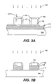
Referring to FIGS. 3A and 3B , the second layer 150, the photoresist structures 130, the ARC layer 120, and the first layer 110 are etched anisotropically with a plasma-based dry etching process. The dry etching process uses plasma 160 as etchant. In an embodiment in which “a” is thicker than “b,” the thickness of the second layer 150 changes from an “a” to “a-b” after the second layer 150 deposited over the ARC layer 120 is completely etched away. This shows that the second layer 150 provides excellent resistance to the plasma etch process and therefore enhances the etching resistance of the photoresist structures 130.
As shown in FIG. 3B , when the anisotropic dry etching process continues, the second layer 150 acts as an etch stop and remains on the sidewalls of the photoresist structures 130. Thus, the dimensions between the patterned photoresist and the underlying patterned first layer 110 are reduced. The photoresist structures 130 may be removed using any conventional process.
Other embodiments of the invention will be apparent to those skilled in the art from consideration of the specification and practice of the invention disclosed herein. It is intended that the specification and examples be considered as exemplary only, with a true scope and spirit of the invention being indicated by the following claims.
Claims (6)
1. A semiconductor manufacturing method, comprising:
defining a substrate;
providing a first layer over the substrate;
providing a layer of photoresist over the first layer;
patterning and defining the photoresist layer to form at least two photoresist structures, wherein each of the photoresist structures includes substantially vertical sidewalls and a substantially horizontal top, and wherein the photoresist structures are separated by a space;
depositing a layer of polymer on the tops of the photoresist structures and the space separating the photoresist structures, wherein an amount of the polymer deposited on the tops of the photoresist structures is substantially greater than an amount of the polymer deposited on the sidewalls of the photoresist structures; and
etching the polymer layer on the tops of the photoresist structures and the space between the photoresist structures, and the first layer.
2. The method as claimed in claim 1 , wherein the layer of polymer is photo-insensitive.
3. The method as claimed in claim 1 , wherein the step of depositing a layer of polymer is provided at a temperature not affecting a stability of the photoresist structures.
4. The method as claimed in claim 1 further comprising a step of depositing an anti-reflection coating over the first layer.
5. The method as claimed in claim 1 , wherein the first layer is a polysilicon layer.
6. The method as claimed in claim 1 , wherein the first layer is a dielectric layer.
Priority Applications (1)
| Application Number | Priority Date | Filing Date | Title |
|---|---|---|---|
| US10/739,049 US7033948B2 (en) | 2001-10-18 | 2003-12-19 | Method for reducing dimensions between patterns on a photoresist |
Applications Claiming Priority (2)
| Application Number | Priority Date | Filing Date | Title |
|---|---|---|---|
| US09/978,546 US6750150B2 (en) | 2001-10-18 | 2001-10-18 | Method for reducing dimensions between patterns on a photoresist |
| US10/739,049 US7033948B2 (en) | 2001-10-18 | 2003-12-19 | Method for reducing dimensions between patterns on a photoresist |
Related Parent Applications (1)
| Application Number | Title | Priority Date | Filing Date |
|---|---|---|---|
| US09/978,546 Division US6750150B2 (en) | 2001-10-18 | 2001-10-18 | Method for reducing dimensions between patterns on a photoresist |
Publications (2)
| Publication Number | Publication Date |
|---|---|
| US20040132225A1 US20040132225A1 (en) | 2004-07-08 |
| US7033948B2 true US7033948B2 (en) | 2006-04-25 |
Family
ID=25526197
Family Applications (2)
| Application Number | Title | Priority Date | Filing Date |
|---|---|---|---|
| US09/978,546 Expired - Lifetime US6750150B2 (en) | 2001-10-18 | 2001-10-18 | Method for reducing dimensions between patterns on a photoresist |
| US10/739,049 Expired - Lifetime US7033948B2 (en) | 2001-10-18 | 2003-12-19 | Method for reducing dimensions between patterns on a photoresist |
Family Applications Before (1)
| Application Number | Title | Priority Date | Filing Date |
|---|---|---|---|
| US09/978,546 Expired - Lifetime US6750150B2 (en) | 2001-10-18 | 2001-10-18 | Method for reducing dimensions between patterns on a photoresist |
Country Status (1)
| Country | Link |
|---|---|
| US (2) | US6750150B2 (en) |
Cited By (5)
| Publication number | Priority date | Publication date | Assignee | Title |
|---|---|---|---|---|
| US20060172540A1 (en) * | 2005-02-03 | 2006-08-03 | Jeffrey Marks | Reduction of feature critical dimensions using multiple masks |
| US20060259886A1 (en) * | 2005-05-10 | 2006-11-16 | Lam Research Corporation | Computer readable mask shrink control processor |
| US20060257750A1 (en) * | 2005-05-10 | 2006-11-16 | Lam Research Corporation | Reticle alignment and overlay for multiple reticle process |
| US20060290012A1 (en) * | 2005-06-28 | 2006-12-28 | Sadjadi S M R | Multiple mask process with etch mask stack |
| US8883648B1 (en) * | 2013-09-09 | 2014-11-11 | United Microelectronics Corp. | Manufacturing method of semiconductor structure |
Families Citing this family (34)
| Publication number | Priority date | Publication date | Assignee | Title |
|---|---|---|---|---|
| US7303995B2 (en) * | 2001-10-18 | 2007-12-04 | Macronix International Co., Ltd. | Method for reducing dimensions between patterns on a photoresist |
| US6750150B2 (en) * | 2001-10-18 | 2004-06-15 | Macronix International Co., Ltd. | Method for reducing dimensions between patterns on a photoresist |
| US6774051B2 (en) * | 2002-06-12 | 2004-08-10 | Macronix International Co., Ltd. | Method for reducing pitch |
| US6756619B2 (en) * | 2002-08-26 | 2004-06-29 | Micron Technology, Inc. | Semiconductor constructions |
| US7351247B2 (en) | 2002-09-04 | 2008-04-01 | Bioconnect Systems, Inc. | Devices and methods for interconnecting body conduits |
| KR100928098B1 (en) * | 2002-12-24 | 2009-11-24 | 동부일렉트로닉스 주식회사 | Metal line formation method using oxide film |
| US7250371B2 (en) * | 2003-08-26 | 2007-07-31 | Lam Research Corporation | Reduction of feature critical dimensions |
| US6924156B2 (en) * | 2003-09-30 | 2005-08-02 | Infineon Technologies Ag | Method for forming a ferroelectric capacitor device |
| US7256126B1 (en) * | 2004-02-03 | 2007-08-14 | Macronix International Co., Ltd. | Pitch reduction integrating formation of memory array and peripheral circuitry |
| US6864184B1 (en) * | 2004-02-05 | 2005-03-08 | Advanced Micro Devices, Inc. | Method for reducing critical dimension attainable via the use of an organic conforming layer |
| US7183205B2 (en) * | 2004-06-08 | 2007-02-27 | Macronix International Co., Ltd. | Method of pitch dimension shrinkage |
| KR100621562B1 (en) * | 2004-07-30 | 2006-09-14 | 삼성전자주식회사 | Method of dry etching using selective polymer mask formed by CO gas |
| US20060134917A1 (en) * | 2004-12-16 | 2006-06-22 | Lam Research Corporation | Reduction of etch mask feature critical dimensions |
| US7491647B2 (en) * | 2005-03-08 | 2009-02-17 | Lam Research Corporation | Etch with striation control |
| US7241683B2 (en) * | 2005-03-08 | 2007-07-10 | Lam Research Corporation | Stabilized photoresist structure for etching process |
| US7695632B2 (en) * | 2005-05-31 | 2010-04-13 | Lam Research Corporation | Critical dimension reduction and roughness control |
| US7273815B2 (en) * | 2005-08-18 | 2007-09-25 | Lam Research Corporation | Etch features with reduced line edge roughness |
| JP2007123766A (en) * | 2005-10-31 | 2007-05-17 | Tokyo Electron Ltd | Etching method, plasma processing apparatus, and storage medium |
| US7220680B1 (en) * | 2005-10-31 | 2007-05-22 | Taiwan Semiconductor Manufacturing Company, Ltd. | Method for photolithography in semiconductor manufacturing |
| US7485581B2 (en) * | 2005-11-30 | 2009-02-03 | Lam Research Corporation | Device with gaps for capacitance reduction |
| US7973366B2 (en) | 2006-02-13 | 2011-07-05 | Macronix International Co., Ltd. | Dual-gate, sonos, non-volatile memory cells and arrays thereof |
| US7407597B2 (en) * | 2006-09-14 | 2008-08-05 | Lam Research Corporation | Line end shortening reduction during etch |
| US7309646B1 (en) | 2006-10-10 | 2007-12-18 | Lam Research Corporation | De-fluoridation process |
| US20080203386A1 (en) * | 2007-02-28 | 2008-08-28 | Ulrich Klostermann | Method of forming a patterned resist layer for patterning a semiconductor product |
| DE102007016321B3 (en) * | 2007-04-04 | 2008-08-21 | Qimonda Ag | Structured resist layer manufacturing method for structuring e.g. reticle mask substrate, involves lithographically exposing resist layer covered with inorganic layer, and structuring resist layer by etching to form structured layer |
| US20080286698A1 (en) * | 2007-05-18 | 2008-11-20 | Haoren Zhuang | Semiconductor device manufacturing methods |
| US8106519B2 (en) * | 2008-04-22 | 2012-01-31 | Macronix International Co., Ltd. | Methods for pitch reduction |
| US9314600B2 (en) | 2012-04-15 | 2016-04-19 | Bioconnect Systems, Inc. | Delivery system for implantable flow connector |
| KR20140020150A (en) * | 2012-08-08 | 2014-02-18 | 에스케이하이닉스 주식회사 | Method of manufacturing a semiconductor device |
| KR20150055473A (en) * | 2013-11-13 | 2015-05-21 | 삼성전자주식회사 | Method for forming carbon-containing layer and method for manufacturing semiconductor device using the same |
| US20180323078A1 (en) * | 2015-12-24 | 2018-11-08 | Intel Corporation | Pitch division using directed self-assembly |
| US10727045B2 (en) * | 2017-09-29 | 2020-07-28 | Taiwan Semiconductor Manufacturing Company, Ltd. | Method for manufacturing a semiconductor device |
| US10566194B2 (en) * | 2018-05-07 | 2020-02-18 | Lam Research Corporation | Selective deposition of etch-stop layer for enhanced patterning |
| CN110931354B (en) * | 2018-09-19 | 2023-05-05 | 中芯国际集成电路制造(上海)有限公司 | Semiconductor structure and method for manufacturing semiconductor structure |
Citations (9)
| Publication number | Priority date | Publication date | Assignee | Title |
|---|---|---|---|---|
| US4586980A (en) | 1984-02-20 | 1986-05-06 | Canon Kabushiki Kaisha | Pattern forming method |
| US4707218A (en) | 1986-10-28 | 1987-11-17 | International Business Machines Corporation | Lithographic image size reduction |
| US4838991A (en) | 1987-10-30 | 1989-06-13 | International Business Machines Corporation | Process for defining organic sidewall structures |
| US4871630A (en) | 1986-10-28 | 1989-10-03 | International Business Machines Corporation | Mask using lithographic image size reduction |
| US4962054A (en) | 1988-04-11 | 1990-10-09 | Sumitomo Electric Industries, Ltd. | Method for manufacturing a field effect transistor using spacers of different thicknesses |
| US5618383A (en) | 1994-03-30 | 1997-04-08 | Texas Instruments Incorporated | Narrow lateral dimensioned microelectronic structures and method of forming the same |
| US5770510A (en) | 1996-12-09 | 1998-06-23 | Vanguard International Semiconductor Corporation | Method for manufacturing a capacitor using non-conformal dielectric |
| US6100014A (en) | 1998-11-24 | 2000-08-08 | United Microelectronics Corp. | Method of forming an opening in a dielectric layer through a photoresist layer with silylated sidewall spacers |
| US6750150B2 (en) * | 2001-10-18 | 2004-06-15 | Macronix International Co., Ltd. | Method for reducing dimensions between patterns on a photoresist |
-
2001
- 2001-10-18 US US09/978,546 patent/US6750150B2/en not_active Expired - Lifetime
-
2003
- 2003-12-19 US US10/739,049 patent/US7033948B2/en not_active Expired - Lifetime
Patent Citations (9)
| Publication number | Priority date | Publication date | Assignee | Title |
|---|---|---|---|---|
| US4586980A (en) | 1984-02-20 | 1986-05-06 | Canon Kabushiki Kaisha | Pattern forming method |
| US4707218A (en) | 1986-10-28 | 1987-11-17 | International Business Machines Corporation | Lithographic image size reduction |
| US4871630A (en) | 1986-10-28 | 1989-10-03 | International Business Machines Corporation | Mask using lithographic image size reduction |
| US4838991A (en) | 1987-10-30 | 1989-06-13 | International Business Machines Corporation | Process for defining organic sidewall structures |
| US4962054A (en) | 1988-04-11 | 1990-10-09 | Sumitomo Electric Industries, Ltd. | Method for manufacturing a field effect transistor using spacers of different thicknesses |
| US5618383A (en) | 1994-03-30 | 1997-04-08 | Texas Instruments Incorporated | Narrow lateral dimensioned microelectronic structures and method of forming the same |
| US5770510A (en) | 1996-12-09 | 1998-06-23 | Vanguard International Semiconductor Corporation | Method for manufacturing a capacitor using non-conformal dielectric |
| US6100014A (en) | 1998-11-24 | 2000-08-08 | United Microelectronics Corp. | Method of forming an opening in a dielectric layer through a photoresist layer with silylated sidewall spacers |
| US6750150B2 (en) * | 2001-10-18 | 2004-06-15 | Macronix International Co., Ltd. | Method for reducing dimensions between patterns on a photoresist |
Cited By (9)
| Publication number | Priority date | Publication date | Assignee | Title |
|---|---|---|---|---|
| US20060172540A1 (en) * | 2005-02-03 | 2006-08-03 | Jeffrey Marks | Reduction of feature critical dimensions using multiple masks |
| US20060259886A1 (en) * | 2005-05-10 | 2006-11-16 | Lam Research Corporation | Computer readable mask shrink control processor |
| US20060257750A1 (en) * | 2005-05-10 | 2006-11-16 | Lam Research Corporation | Reticle alignment and overlay for multiple reticle process |
| US7465525B2 (en) | 2005-05-10 | 2008-12-16 | Lam Research Corporation | Reticle alignment and overlay for multiple reticle process |
| US7539969B2 (en) | 2005-05-10 | 2009-05-26 | Lam Research Corporation | Computer readable mask shrink control processor |
| US20060290012A1 (en) * | 2005-06-28 | 2006-12-28 | Sadjadi S M R | Multiple mask process with etch mask stack |
| WO2007001647A1 (en) * | 2005-06-28 | 2007-01-04 | Lam Research Corporation | Multiple mask process with etch mask stack |
| US7271108B2 (en) * | 2005-06-28 | 2007-09-18 | Lam Research Corporation | Multiple mask process with etch mask stack |
| US8883648B1 (en) * | 2013-09-09 | 2014-11-11 | United Microelectronics Corp. | Manufacturing method of semiconductor structure |
Also Published As
| Publication number | Publication date |
|---|---|
| US20030082916A1 (en) | 2003-05-01 |
| US6750150B2 (en) | 2004-06-15 |
| US20040132225A1 (en) | 2004-07-08 |
Similar Documents
| Publication | Publication Date | Title |
|---|---|---|
| US7033948B2 (en) | Method for reducing dimensions between patterns on a photoresist | |
| JP5894622B2 (en) | Method for etching a silicon-containing hard mask | |
| US7361607B2 (en) | Method for multi-layer resist plasma etch | |
| KR20010032912A (en) | Method for etching silicon oxynitride and inorganic antireflection coatings | |
| US20090081879A1 (en) | Method for manufacturing semiconductor device | |
| US20130109188A1 (en) | Plasma etch processes for boron-doped carbonaceous mask layers | |
| US7635649B2 (en) | Method for manufacturing semiconductor device | |
| US20050048789A1 (en) | Method for plasma etching a dielectric layer | |
| US7943520B2 (en) | Hole pattern forming method and semiconductor device manufacturing method | |
| KR20030022361A (en) | Method of etching titanium nitride | |
| US20110253670A1 (en) | Methods for etching silicon-based antireflective layers | |
| US7352064B2 (en) | Multiple layer resist scheme implementing etch recipe particular to each layer | |
| US6946400B2 (en) | Patterning method for fabricating integrated circuit | |
| Park et al. | Effects of CH2F2 and H2 flow rates on process window for infinite etch selectivity of silicon nitride to ArF PR in dual-frequency CH2F2/H2/Ar capacitively coupled plasmas | |
| US7361604B2 (en) | Method for reducing dimensions between patterns on a hardmask | |
| US6828251B2 (en) | Method for improved plasma etching control | |
| US6921723B1 (en) | Etching method having high silicon-to-photoresist selectivity | |
| JP2003158072A (en) | Method for reducing size between patterns of photoresist | |
| US7303995B2 (en) | Method for reducing dimensions between patterns on a photoresist | |
| US20030235998A1 (en) | Method for eliminating standing waves in a photoresist profile | |
| US6573177B1 (en) | Protection layer to prevent under-layer damage during deposition | |
| US20060292883A1 (en) | Etching of silicon nitride with improved nitride-to-oxide selectivity utilizing halogen bromide/chlorine plasma | |
| US6699792B1 (en) | Polymer spacers for creating small geometry space and method of manufacture thereof | |
| US20030224254A1 (en) | Method for reducing dimensions between patterns on a photomask | |
| US6828250B1 (en) | Process for etching vias in organosilicate glass materials without causing RIE lag |
Legal Events
| Date | Code | Title | Description |
|---|---|---|---|
| STCF | Information on status: patent grant |
Free format text: PATENTED CASE |
|
| FPAY | Fee payment |
Year of fee payment: 4 |
|
| FPAY | Fee payment |
Year of fee payment: 8 |
|
| MAFP | Maintenance fee payment |
Free format text: PAYMENT OF MAINTENANCE FEE, 12TH YEAR, LARGE ENTITY (ORIGINAL EVENT CODE: M1553) Year of fee payment: 12 |