US7042736B2 - Storage apparatus and shielding method for storage apparatus - Google Patents
Storage apparatus and shielding method for storage apparatus Download PDFInfo
- Publication number
- US7042736B2 US7042736B2 US10/774,534 US77453404A US7042736B2 US 7042736 B2 US7042736 B2 US 7042736B2 US 77453404 A US77453404 A US 77453404A US 7042736 B2 US7042736 B2 US 7042736B2
- Authority
- US
- United States
- Prior art keywords
- rack
- disk
- parts
- electrical conductivity
- housed
- Prior art date
- Legal status (The legal status is an assumption and is not a legal conclusion. Google has not performed a legal analysis and makes no representation as to the accuracy of the status listed.)
- Expired - Fee Related, expires
Links
Images


Classifications
-
- G—PHYSICS
- G11—INFORMATION STORAGE
- G11B—INFORMATION STORAGE BASED ON RELATIVE MOVEMENT BETWEEN RECORD CARRIER AND TRANSDUCER
- G11B33/00—Constructional parts, details or accessories not provided for in the other groups of this subclass
- G11B33/12—Disposition of constructional parts in the apparatus, e.g. of power supply, of modules
- G11B33/125—Disposition of constructional parts in the apparatus, e.g. of power supply, of modules the apparatus comprising a plurality of recording/reproducing devices, e.g. modular arrangements, arrays of disc drives
- G11B33/126—Arrangements for providing electrical connections, e.g. connectors, cables, switches
-
- G—PHYSICS
- G11—INFORMATION STORAGE
- G11B—INFORMATION STORAGE BASED ON RELATIVE MOVEMENT BETWEEN RECORD CARRIER AND TRANSDUCER
- G11B33/00—Constructional parts, details or accessories not provided for in the other groups of this subclass
- G11B33/14—Reducing influence of physical parameters, e.g. temperature change, moisture, dust
- G11B33/1493—Electro-Magnetic Interference [EMI] or Radio Frequency Interference [RFI] shielding; grounding of static charges
Definitions
- the present invention relates to a storage apparatus and to a shielding method for a storage apparatus.
- the storage apparatuses are required to have extremely high reliability, and so positive interception of electromagnetic waves is particularly important. For this reason, storage apparatuses adopt various shielding structures for intercepting electromagnetic waves.
- a multiplicity of electronic component parts are incorporated at high density in a storage apparatus. Therefore, with respect to a storage apparatus, it is strongly desired to realize simplified manufacture, improved maintainability, reduced manufacturing cost and a reduced number of component parts, while strengthening the interception of electromagnetic waves.
- the present invention has been made in view of the above-described problem and mainly provides a storage apparatus and a shielding method for a storage apparatus.
- the invention provides a storage apparatus which includes a storage control section including a first rack having electrical conductivity, and channel control parts and disk control parts housed in the first rack.
- the channel control parts are communicably connected to an information processing apparatus and are constructed to receive a data input/output request from the information processing apparatus.
- the disk control parts are communicably connected to hard disk drives for storing data and are constructed to perform read/write operations on data from and to the hard disk drives in response to a data input/output request from the information processing apparatus.
- the storage apparatus further includes a storage drive section including a second rack having electrical conductivity, the aforementioned hard disk drives, and relay parts for relaying communications between the hard disk drives and the disk control parts.
- the hard disk drives and the relay parts are housed in the second rack.
- communication cables are provided for communicably connecting the disk control parts to the relay parts.
- Each of the communication cables includes a transmission medium through which to transmit data to be read or written by the disk control parts, a first conductor having electrical conductivity and surrounding the transmission medium with an insulator interposed therebetween, a second conductor having electrical conductivity and surrounding the first conductor with an insulator interposed therebetween, and an electrically nonconductive covering surrounding the second conductor.
- the first conductor is electrically conductibly connected to ground potential supply circuits provided in at least either the disk control parts or the relay parts
- the second conductor is electrically conductibly connected to at least one of the first rack and the second rack.
- FIG. 1 is a perspective view showing the external appearance and construction of a storage apparatus according to an embodiment of the invention
- FIGS. 2A and 2B are perspective views showing the external appearance and construction of a typical control section according to the invention, FIG. 2A being a front perspective view as seen from the right and FIG. 2B being a rear perspective view as seen from the left;
- FIG. 3 is a front perspective view showing the external appearance of a typical one of the drive sections according to the invention.
- FIG. 4 is a perspective view showing the state in which control boxes are housed in the control section according to the invention.
- FIG. 5 is a perspective view showing the state in which disk drive boxes are housed in one of the drive sections according to the invention.
- FIG. 6 is a block diagram showing an example of the internal construction of the storage apparatus according to the invention.
- FIG. 7 is a block diagram showing the state in which disk adapters and storage volumes are communicably connected to one another according to the invention.
- FIG. 8 is a perspective view showing the construction of another drive section
- FIG. 9 is a perspective view showing one of the drive sections according to the invention.
- FIG. 10 is a front view showing the external appearance of one example of the connection between disk adapters and hard disk drives according to the invention.
- FIG. 11 is a front view showing an external appearance of another example of the connection between disk adapters and hard disk drives according to the invention.
- FIG. 12 is a schematic diagram showing the state of connection between disk adapters and hard disk drives according to the invention.
- FIG. 13 is a front view showing the external appearance of the state of connection between disk adapters and hard disk drives according to the invention.
- FIG. 14 is a diagram showing a communication cable and a cross-section along line A—A thereof according to the invention.
- FIG. 15 is a front view showing the state in which Fibre Channel switches according to the invention are fitted.
- FIG. 16 includes an exploded perspective view and an assembled perspective view showing the state in which frame ground potential is supplied to communication cables in the storage apparatus according to the invention
- FIG. 17 includes a front view and a side view showing the state in which frame ground potential is supplied to communication cables in the storage apparatus according to the invention
- FIG. 18 is a diagram showing a communication cable and a cross-section along line B—B thereof according to the invention.
- FIG. 19 is a front view showing the external appearance of the connection between disk adapters and hard disk drives according to the invention.
- FIG. 20 is a diagram showing the state in which a communication cable is routed in a storage device according to the invention.
- FIG. 21 is a diagram showing the state in which a communication cable is routed in a storage device according to the invention.
- FIG. 22 is a perspective view showing the state in which communication cables are connected to Fibre Channel switches according to the invention.
- FIG. 23 is a perspective view showing the state in which covers are respectively provided on Fibre Channel switches according to the invention.
- FIG. 24A is a sectional view and FIG. 24B is a perspective view showing the state in which a communication cable is routed in a storage device according to the invention
- FIG. 25A is a sectional view and FIG. 25B is a perspective view thereof showing the state in which a communication cable is routed in a storage device according to the invention
- FIG. 26 is a developed perspective view showing the state in which a cover is provided on a control box according to the invention.
- FIG. 27 is a developed perspective view showing the state in which rack covers are provided on one of the drive sections according to the invention.
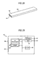
- FIG. 28 is a perspective view showing an elastic body having electrical conductivity according to the invention.
- FIG. 29 is a block diagram showing the construction of a channel adapter according to the invention.
- FIG. 30 is a block diagram showing the construction of a disk adapter according to the invention.
- FIG. 31 is a developed perspective view showing the state in which rack covers are provided on the control section according to the invention.
- FIG. 1 An example of the external appearance and construction of a storage apparatus (hereinafter referred to also as a disk array apparatus) 100 according to one embodiment of the invention will be described with reference to FIG. 1 .
- a storage apparatus hereinafter referred to also as a disk array apparatus
- the disk array apparatus 100 shown in FIG. 1 includes a control section (a storage control section) 110 and drive sections (storage drive sections) 120 .
- the control section 110 is disposed in the middle of the disk array apparatus 100
- the drive sections 120 are disposed on the right and left sides of the control section 110 .
- the control section 110 is responsible for controlling the entire disk array apparatus 100 .
- logical parts 420 that are responsible for controlling the entire disk array apparatus 100 and disk drive units 310 for storing data are disposed on the front and rear sides of the control section 110 .
- Disk drive units 310 are disposed on the front and rear sides of the drive sections 120 .
- the disk array apparatus 100 contains various electronic devices at a high density so that its large data storage capacity and a reduction in size can be compatibly realized.
- the disk array apparatus 100 is also provided with various constructions for intercepting electromagnetic waves from the outside. Detailed constructions of the control section 110 and the drive sections 120 will be described below with reference to FIGS. 2A through 5 .
- FIGS. 2A , 2 B and 4 show the construction of the control section 110 .
- FIG. 2A shows a front perspective view of the external appearance of the control section 110 , as seen from the right direction
- FIG. 2B shows a rear perspective view of the external appearance of the control section 110 , as seen from the left direction.
- the external appearance shown in FIG. 2A corresponds to the front perspective view of the external appearance seen from the right direction
- the external appearance shown in FIG. 2B corresponds to the rear perspective view of the external appearance seen from the left direction.
- the control section 110 has an approximately rectangular parallelepipedic framework (a first rack) 200 having electrical conductivity, in which disk drive modules (disk boxes) 300 , logical modules (control boxes) 400 , batteries 800 , AC-BOXES 700 , AC/DC power sources 600 , fans 500 and an operator panel 111 are housed.
- the framework 200 may be made of, for example, a metal having electrical conductivity.
- Each of the disk drive modules 300 has an approximately rectangular parallelepipedic shape as well as electrical conductivity.
- Each of the disk drive modules 300 may be made of, for example, a metal having electrical conductivity.
- the disk drive modules 300 are housed in the upper portion of the framework 200 so that the disk drive modules 300 are electrically conductibly connected to the framework 200 .
- a plurality of disk drive units 310 are housed in each of the disk drive modules 300 in such a manner that each of the disk drive units 310 is adjacent to the next one and is removably inserted in the disk drive modules 300 , as seen in FIG.
- Fibre Channel switches (FSWs or relay parts) 150 are also housed in each of the disk drive modules 300 so that each of the Fibre Channel switches 150 can be removably inserted in the disk drive modules 300 .
- the disk drive modules 300 and the framework 200 may be arranged to conduct electricity therebetween by being connected to each other by electrical cables, or by being brought into simple physical contact with each other.
- Each of the disk drive units 310 is constructed in such a manner that a disk drive (hard disk drive) for storing data is housed in a canister.
- the FSWs 150 will be described later.
- Each of the logical modules 400 has electrical conductivity and an approximately rectangular parallelepipedic shape.
- the logical modules 400 may be made of, for example, a metal having electrical conductivity.
- the logical modules 400 are housed in the middle portion of the framework 200 so that the logical modules 400 are electrically conductibly connected to the framework 200 .
- the logical modules 400 and the framework 200 may be arranged to conduct electricity therebetween by being connected to each other by electrical cables, or by being brought into simple physical contact with each other.
- Each of the logical modules 400 is provided with a logical part 420 and logical module fans 410 , as seen in FIG. 4 .
- Control boards 430 provided with various functions for controlling read/write of data from and to disk drives 311 are housed in the logical part 420 so that each of the control boards 430 is removably inserted in the logical part 420 . Although the details thereof will be described later, as shown in FIG.
- each of the circuit boards 430 of the logical part 420 includes channel adapters (channel control parts which are communicably connected to an information processing apparatus 1000 and receive a data input/output request from the information processing apparatus 1000 ) 131 , a cache memory 133 , a shared memory 135 , a connection part 132 , and disk adapters (disk control parts which are communicably connected to hard disk drives for storing data and perform read/write of data from and to the hard disk drives in response to a data input/output request) 134 .
- the logical module fans 410 are devices for producing cooling air to cool the logical part 420 . Cooling air enters the inside of the framework 200 from the front side of the logical modules 400 through the gap between each of the circuit boards 430 of the logical parts 420 , and it is discharged from the ceiling portion of the framework 200 to the outside thereof by being drawn by the logical module fans 410 and fans 500 .
- the batteries 800 , the AC-BOXES 700 and the AC/DC power sources 600 are housed in the lower portion of the framework 200 .
- the batteries 800 , the AC-BOXES 700 and the AC/DC power sources 600 are hereinafter referred to also as a power source part.
- the AC-BOXES 700 constitute inlets for introducing alternating current power into the disk array apparatus 100 , and they function as a breaker. Alternating current power introduced into the AC-BOXES 700 is supplied to the AC/DC power sources 600 .
- the AC/DC power sources 600 are power source units for converting the introduced alternating current voltage to direct current voltage and for outputting direct current voltage to be supplied to the logical parts 420 , the disk drive units 310 and the like.
- the batteries 800 are power storage units for supplying direct current power to various devices provided in the control section 110 instead of the AC/DC power sources 600 during a failure in the supply of direct current power from the AC/DC power sources 600 , such as a power failure or an abnormality occurring in the AC/DC power sources 600 .
- the fans 500 are disposed on the ceiling portion of the framework 200 .
- the fans 500 are units for producing cooling air to cool the control section 110 . Cooling air enters the inside of the framework 200 from the front side of each of the disk drive modules 300 and the logical modules 400 , and it is discharged to the outside of the framework 200 by being drawn by the fans 500 .
- the operator panel 111 is disposed on the front side of the framework 200 .
- the operator panel 111 is a unit for accepting operation inputs from an operator who performs maintenance and management on the disk array apparatus 100 .
- FIGS. 3 and 5 show the construction of a typical one of the drive sections 120 .
- FIG. 3 is a front perspective view showing the external appearance of one of the drive sections 120 , as seen from the right direction.
- the drive section 120 shown in FIG. 3 has an approximately rectangular parallelepipedic framework (a second rack) 200 having electrical conductivity, in which disk drive modules (disk boxes) 300 , batteries 800 , AC-BOXES 700 , AC/DC power sources 600 and fans 500 are housed.
- the devices provided in the drive section 120 are the same as the corresponding devices provided in the control section 110 .
- the framework 200 used in the control section 110 and the framework 200 used in each of the drive sections 120 can be constructed with the same structure. In this case, if the logical modules 400 are housed in the middle portion of the framework 200 , it is possible to provide the control section 110 , whereas if the disk drive modules 300 are housed in the middle portion of the framework 200 , it is possible to provide the drive section 120 .
- FIG. 6 is a block diagram showing an example of the internal construction of the disk array apparatus 100 according to this embodiment of the invention.
- the disk array apparatus 100 is communicably connected to an information processing apparatus 1000 via a SAN (Storage Area Network) 900 .
- SAN Storage Area Network
- the information processing apparatus 1000 is an information apparatus, such as a computer having a CPU (Central Processing Unit) and memories. Various functions can be realized by various programs being executed by the CPU provided in the information processing apparatus 1000 .
- the information processing apparatus 1000 can be used as, for example, a main computer in an ATM cash dispenser system for banks or a seat reservation system for airlines.
- the SAN 900 is a network for exchange of data between the information processing apparatus 1000 and the disk array apparatus 100 .
- the communication performed between the information processing apparatus 1000 and the disk array apparatus 100 via the SAN 900 obeys the Fibre Channel Protocol.
- a data input/output request is transmitted from the information processing apparatus 1000 to the disk array apparatus 100 in accordance with the Fibre Channel Protocol.
- the disk array apparatus 100 is provided with a disk array control part 130 and disk array drive parts 140 .
- the disk array control part 130 is arranged in the control section 110
- the disk array drive parts 140 are arranged in the control section 110 or the drive sections 120 .
- the control section 110 is provided with the disk array control part 130 and the disk array drive parts 140
- the respective drive sections 120 are provided with the disk array drive parts 140 .
- the disk array control part 130 receives a data input/output request from the information processing apparatus 1000 , and performs read/write of data from and to the disk drives 311 provided in the disk array drive parts 140 .
- the disk array control part 130 includes the channel adapters 131 , the cache memory 133 , the connection part 132 , the shared memory 135 , the disk adapters (hereinafter referred to also as DKFs) 134 , and a management terminal (hereinafter referred to also as an SVP) 136 .
- the channel adapters 131 , the cache memory 133 , the connection part 132 , the shared memory 135 and the disk adapters 134 are constructed on the circuit boards 430 which constitute each of the logical parts 420 shown in FIG. 4 .
- the channel adapters 131 which are communicably connected to the information processing apparatus 1000 , receive a data input/output request from the information processing apparatus 1000 and perform exchange of data with the information processing apparatus 1000 .
- each of the channel adapters 131 is constructed as part of one unit board provided with a circuit board.
- Each of the channel adapters 131 includes a network interface part 451 , a memory 453 , an input/output control part 454 , an I/O (Input/Output) processor 459 , a NVRAM (Non-Volatile RAM) 455 , a board-connecting connector 456 , and a communication connector 457 .
- Other circuits similar to those of general electronic circuits, such as a voltage supply circuit and a ground potential supply circuit, are provided on the circuit board of each of the channel adapters 131 .
- the network interface part 451 is provided with a communication interface for establishing communication with the information processing apparatus 1000 .
- the network interface part 451 receives a data input/output request transmitted from the information processing apparatus 1000 in accordance with the Fibre Channel Protocol.
- the communication connector 457 is a connector to which a cable, via which the network interface part 451 communicates with the information processing apparatus 1000 , is to be connected.
- the communication connector 457 supports, for example, the Fibre Channel.
- the input/output control part 454 is responsible for controlling the entire channel adapter 131 , and it performs exchange of data and commands with the disk adapters 134 , the cache memory 133 , the connection part 132 and the management terminal 136 .
- the input/output control part 454 executes various programs stored in the memory 453 , thereby realizing various functions of the channel adapter 131 .
- the input/output control part 454 is provided with the I/O processor 459 and the NVRAM 455 .
- the I/O processor 459 controls the exchange of data and commands.
- the NVRAM 455 is a non-volatile memory which stores a program responsible for control of the I/O processor 459 . The content of the program which is stored in the NVRAM 455 can be written and rewritten from the management terminal 136 .
- the cache memory 133 and the shared memory 135 are memories which store data and commands to be exchanged between the channel adapter 131 and the disk adapters 134 . For example, if a data input/output request which a channel adapter 131 has received from the information processing apparatus 1000 is a write request, the channel adapter 131 writes the write request to the shared memory 135 , and it also writes to the cache memory 133 data received from the information processing apparatus 1000 . Then, the corresponding one of the disk adapters 134 reads the data written to the cache memory 133 and writes the read data to the corresponding one of the disk drives 311 in accordance with the write request written to the shared memory 135 .
- connection part 132 provides interconnections among the channel adapters 131 , the shared memory 135 , the cache memory 133 and the disk adapters 134 .
- the connection part 132 includes, for example, a crossbar switch.
- Each of the disk adapters 134 is communicably connected to the corresponding ones of the disk drives 311 and performs read/write of data from and to the corresponding ones of the disk drives 311 by communicating therewith.
- the read/write of data is performed via a communication path which constitutes a loop determined by FC-AL, which is a Fibre Channel Standard (hereinafter referred to also as the FC-AL loop).
- the communication path includes the disk adapters 134 , communication cables 160 , the FSWs 150 , and the disk drives 311 .
- each of the disk adapters 134 and the corresponding ones of the disk drives 311 is relayed by the FSW 150 provided in each of the disk array drive parts 140 .
- FIG. 30 The hardware construction of a typical one of the disk adapters 134 is shown in FIG. 30 .
- the hardware of each of the disk adapters 134 is constructed as part of one unit board provided with a circuit board.
- Each of the disk adapters 134 includes an interface part 461 , a memory 463 , an input/output control part 462 , a NVRAM (Non-Volatile RAM) 464 , a board-connecting connector 465 , and communication connectors 466 .
- Other circuits similar to those of general electronic circuits, such as a source voltage supply circuit and a ground potential supply circuit, are provided on the circuit board of each of the disk adapters 134 .
- the interface part 461 is provided with a communication interface for establishing communication with the corresponding ones of the disk drives 311 . Predetermined ones of the communication cables 160 are connected to the communication connector 466 .
- the CPU 462 is responsible for controlling the entire disk adapter 134 .
- the CPU 462 executes various programs stored in the memory 463 and the NVRAM 464 , thereby realizing various functions of the disk adapter 134 .
- the NVRAM 464 is a non-volatile memory which stores a program responsible for control of the CPU 462 .
- the content of the program which is stored in the NVRAM 464 can be written and rewritten from the management terminal 136 .
- the management terminal 136 is an information processing device for effecting maintenance and management of the disk array apparatus 100 .
- the management terminal 136 may be, for example, a notebook computer provided with a display and a keyboard which are constructed in a foldable form.
- the management terminal 136 is housed in the control section 110 .
- the management terminal 136 need not be housed in the control section 110 , and it may also be, for example, a remote computer connected to the disk array apparatus 100 via a communications network.
- the form of the management terminal 136 is not limited to a notebook computer, and it may also be, for example, a desktop computer.
- the management terminal 136 may be an information processing device for exclusively effecting maintenance and management of the disk array apparatus 100 , or it may also be a general-purpose information processing device to which a function for effecting maintenance and management of the disk array apparatus 100 is added.
- channel adapters 131 , the disk adapters 134 , the cache memory 133 , the shared memory 135 and the connection part 132 need not be separately provided, and they may also be constructed in an integrated form. In addition, a combination of at least any two of these circuits may also be constructed in an integrated form.
- FIG. 7 shows the construction of each of the FSWs 150 and the FC-AL loop which is formed by one of the disk adapters 134 , the FSWs 150 , the disk drives 311 and the communication cables 160 .
- the FC-AL loop can be formed by connecting the disk adapter 134 and the disk drives 311 to multiplexers 151 provided in the FSWs 150 .
- one FC-AL loop is formed across two FSWs 150 .
- One of the FSWs 150 is communicably connected to the disk adapter 134 and to the other FSW 150 via the communication cables 160 connected to connectors 153 .
- the disk drives 311 are also communicably connected to each of the FSWs 150 .
- the connections between the disk drives 311 and the FSWs 150 can also be provided by, for example, data transfer paths on a circuit board provided inside each of the drive sections 120 .
- the disk drives 311 and the FSWs 150 may also be connected via the communication cables 160 .
- a select signal applied to each of the multiplexers 151 is a signal for selecting either the input to a side indicated by “1” or the input to a side indicated by “0” in each of the multiplexers 151 .
- the select signal is inputted so that the input to the side indicated by “1” of each of the multiplexers 151 is selected.
- the select signal is inputted to this multiplexer 151 so that the input to the side indicated by “0” is selected.
- the select signal is inputted to a multiplexer 151 to which the particular disk drive 311 is connected, so that the input to the side indicated by “0” is selected.
- Control of the select signal to be inputted to each of the multiplexers 151 is performed by, for example, the corresponding one of control parts 152 .
- the control parts 152 exert control on the respective FSWs 150 .
- To control the FSWs 150 is to control the select signals to be inputted to, for example, the respective multiplexers 151 .
- the control of the select signals by the control parts 152 is performed, for example, when a particular one of the disk drives 311 is to be set to a state communicable or non-communicable with the disk adapters 134 .
- the AC/DC power sources 600 are housed in the lower portion of the framework 200 , and some of the FSWs 150 are housed between the upper and lower ones of the disk drive units 310 housed in the upper portion of each of the disk drive modules 300 , while the other are housed between the upper and lower ones of the disk drive units 310 housed in the lower portion of the same disk drive module 300 .
- AC/DC power sources 1600 and FSWs 1150 are housed in the state of being juxtaposed to disk drive units 1310 in each disk drive module 1300 .
- the lateral width W 2 of the drive section 120 can be made smaller than the lateral width W 1 of the drive section 1120 . Accordingly, it is possible to reduce the overall size of the drive section 120 .
- FIGS. 10 to 13 show an example of the routing of the communication cables 160 from the disk adapters 134 provided in the control section 110 to the disk drives 311 provided in the control section 110 or the drive sections 120 .
- FIG. 10 is a view showing the external appearance of the routing of the communication cables 160 in the disk array apparatus 100 having a construction provided with two disk adapters 134 .
- FIG. 11 is a view showing the external appearance of a routing of the communication cables 160 in the disk array apparatus 100 having a construction provided with four disk adapters 134 .
- FIG. 12 is a diagram showing the connection relationship between the disk adapters 134 and the FSWs 150 .
- FIG. 13 is a diagram schematically showing a routing of the communication cables 160 from the disk adapters 134 to the disk drives 311 .
- the communication cables 160 which communicably interconnect the disk adapters 134 , the FSWs 150 and the disk drives 311 are disposed to reach every location in the inside of the disk array apparatus 100 .
- the disk array apparatus 100 is required to have a structure which does not allow the communication cables 160 to function as an antenna receiving electromagnetic waves radiated from the outside of the disk array apparatus 100 .
- the communication between the disk adapters 134 and the disk drives 311 is performed in accordance with the Fibre Channel Standard, and the speed of the communication reaches several gigahertz (approximately 1 to 4 gigahertz). In this manner, signals of high frequency flow in the communication cables 160 , so that strong electromagnetic waves are radiated from the communication cables 160 . Accordingly, the disk array apparatus 100 is required to intercept electromagnetic waves radiated from the communication cables 160 .
- Strong electromagnetic waves are radiated from not only the communication cables 160 , but also from the channel adapters 131 , the disk adapters 134 , the FSWs 150 and the AC/DC power sources 600 . Accordingly, there is also a need for a structure which intercepts the electromagnetic waves that are radiated from these circuit devices, such as the channel adapters 131 and the FSWs.
- each of the communication cables 160 has the structure shown in FIG. 14 .
- the communication cables 160 has a structure in which a cable 168 has connectors 161 at its opposite ends.
- One of the connectors 161 is connected to the communication connectors 466 of any one of the disk adapters 134 , while the other is connected to the connector 153 of any one of the FSWs 150 .
- the cable 168 has a transmission medium 162 through which data to be read or written by the connected disk adapter 134 is to be transmitted, a first shield (conductor) 164 which has electrical conductivity and surrounds the transmission medium 162 with an insulator 163 interposed therebetween, a second shield (conductor) 166 which has electrical conductivity and surrounds the first shield 164 with an insulator 165 interposed therebetween, and an electrically nonconductive covering 167 which surrounds the second shield 166 .
- the transmission medium 162 may be made of, for example, annealed copper wire.
- the annealed copper wire may be plated with, for example, tin.
- the insulators 163 and 165 may be made of, for example, vinyl chloride or polyethylene foam.
- the first shield 164 may have a structure made of, for example, woven annealed copper wire.
- the first shield 164 may also be made of, for example, polyester tape on which aluminum foil is stuck.
- the second shield 166 may have a structure made of, for example, woven annealed copper wire.
- the second shield 166 may also be made of, for example, polyester tape on which aluminum foil is stuck.
- the covering 167 may be made of, for example, vinyl chloride.
- the first shield 164 is electrically conductibly connected to pins of the respective connectors 161 in the inside of the cable 168 .
- the first shield 164 can be electrically conductibly connected to the ground potential supply circuit provided in at least one of the connected disk adapter 134 and FSW 150 . Accordingly, the potential of the first shield 164 can be set to ground potential, whereby interception of electromagnetic waves can be effected.
- FIG. 15 shows the state in which the communication cables 160 are respectively connected to the connectors 153 of the FSWs 150 .
- up to four FSWs 150 can be fitted in one disk drive module 300 , as shown in FIG. 15 , and as viewed in FIG. 15 , two right-hand ones of the FSWs 150 and the other two left-hand ones differ from each other in fitting height.
- the FSWs 150 according to the embodiment can be removably fitted into the disk drive modules 300 , and the respective FSWs 150 are fitted with levers for fixing or releasing them to or from the disk drive module 300 . As shown in FIG.
- the two right-hand FSWs 150 and the two left-hand FSWs 150 are made different from each other in the height of their fitting positions, whereby interference between the levers of the two right-hand FSWs 150 and the levers of the two left-hand FSWs 150 is prevented. Accordingly, the distance between the right-hand and left-hand FSWs 150 can be made narrow and the width W 2 of each of the drive sections 120 can be made small.
- the second shield 166 of the communication cable 160 is communicably connected to the framework 200 .
- the framework 200 to which the second shield 166 is connected is the framework 200 of the control section 110 , the framework 200 of each of the drive sections 120 , or the frameworks 200 of both sections 110 and 120 .
- the second shield 166 and the framework 200 can be arranged to conduct electricity therebetween, by being connected to each other by an electrical cable or the like, or by being connected to each other by the use of frame ground supply parts (ground potential supply parts) 170 , which will be described below.
- FIGS. 6 and 7 show that the communication cables 160 are connected to ground.
- this illustration shows that the first shield 164 is communicably connected to at least any one of the ground potential supply circuits provided in the disk adapter 134 and the FSW 150 , and the second shield 166 is electrically conductibly connected to the framework 200 .
- the frame ground supply parts 170 are electrically conductibly fixed to each of the logical modules 400 and the disk drive modules 300 . Accordingly, the frame ground supply parts 170 are provided electrically conductibly to at least either the logical modules 400 or the disk drive modules 300 .
- FIG. 16 shows a typically one of the frame ground supply parts 170 .
- the frame ground supply part 170 includes a first cable clamping member (a first communication cable clamping part) 171 which has electrical conductivity and a first surface 174 , a second cable clamping member (a second communication cable clamping part) 172 which has electrical conductivity and is electrically conductibly connected to at least either the framework 200 of the control section 110 or the framework 200 of any of the drive sections 120 and has a second surface 175 .
- a cable fixing part (a fixing part) 173 fixes the first cable clamping member 171 and the second cable clamping member 172 so that the members 171 and 172 are pressed against each other with the first surface 174 and the second surface 175 facing each other.
- the frame ground supply part 170 shown in FIG. 16 is constructed so that the first cable clamping member 171 and the second cable clamping member 172 are separable from each other, but the first cable clamping member 171 and the second cable clamping member 172 may be joined together by hinges or the like.
- a method of electrically conductibly connecting the second shields 166 of the respective communication cables 160 to the framework 200 by the use of the frame ground supply part 170 is as follows. Namely, as shown in FIG. 16 , each of the communication cables 160 has a portion from which the covering 167 is removed around its periphery, and the portions of the respective communication cables 160 are held by being clamped between the first surface 174 of the first cable clamping member 171 and the second surface 175 of the second cable clamping member 172 .
- the second shields 166 are electrically conductibly connected to the frame ground supply part 170 , the second shields 166 can be electrically conductibly connected to the framework 200 .
- the potential of each of the second shields 166 can be maintained at ground potential, whereby interception of electromagnetic waves can be realized. Accordingly, in the disk array apparatus 100 according to this embodiment of the invention, the effect of interception of electromagnetic waves by the first shield 164 and the effect of interception of electromagnetic waves by the second shield 166 are mutually potentiated, whereby data to be read and written from and to the disk drives 311 can be strongly protected from external electromagnetic waves.
- the electrical connection between the second shields 166 and the framework 200 can be provided merely by clamping the portions of the communication cables 160 from which the respective coverings 167 are removed, by the use of the frame ground supply part 170 , whereby the work of routing the communication cables 160 becomes easy. Accordingly, it is possible to facilitate the manufacture and maintenance of the disk array apparatus 100 and the reduce manufacturing cost. In addition, since the communication cables 160 are clamped by the frame ground supply part 170 , it is possible to positively provide electrical connection between the second shields 166 and the framework 200 . Accordingly, it is possible to improve the reliability of the disk array apparatus 100 .
- hollow portions 176 are formed in at least one of the first surface 174 and the second surface 175 .
- This construction makes it possible to increase the area of contact between each of the second shields 166 and the frame ground supply part 170 , whereby electric conductivity is improved between the second shield 166 and the framework 200 and the effect of interception of electromagnetic waves by the second shield 166 can be made far stronger.
- the frame ground supply part 170 can also have the structure shown in FIG. 17 . Namely, the second surface 175 of the second cable clamping member 172 does not have the hollow portions 176 , but the hollow portions 176 are formed on the first surface 174 of the first cable clamping member 171 . This structure makes it possible to facilitate manufacture of the frame ground supply parts 170 and reduce the manufacturing cost.
- the disk array apparatus 100 it is possible to positively effect interception of electromagnetic waves within each of the communication cables 160 , whereby there is no need to provide a special structure for interception of electromagnetic waves.
- a disk array apparatus using communication cables 1160 of the type shown in FIG. 18 there is a need for a special structure for interception of electromagnetic waves, as shown in FIGS. 19 and 20 .
- the communication cable 1160 shown in FIG. 18 has a structure in which a cable 1168 has connectors 1161 at its opposite ends. One of the connectors 1161 is connected to a communication connector of any one of disk adapters 1134 , while the other is connected to a connector of any one of FSWs 1150 .
- the cable 1168 has a transmission medium 1162 through which data to be read or written by the connected disk adapter 1134 is to be transmitted, a first shield 1164 which has electrical conductivity and surrounds the transmission medium 1162 with an insulator 1163 interposed therebetween, and an electrically nonconductive covering 1167 which surrounds the first shield 1164 .
- the first shield 1164 is electrically conductibly connected to pins of the respective connectors 1161 in the inside of the cable 1168 .
- the first shield 1164 is electrically conductibly connected to the ground potential supply circuit provided in at least one of the connected disk adapter 1134 and FSW 1150 . Accordingly, the potential of the first shield 1164 is maintained at ground potential, whereby interception of electromagnetic waves can be effected.
- the communication cable 1160 shown in FIG. 18 is not able to intercept electromagnetic waves passing through the first shield 1164 . Accordingly, in the control section 1100 and the drive sections 1200 , each of which uses the communication cables 1160 of the type shown FIG. 18 , the respective communication cables 1160 need to be covered with communication cable holding parts 1180 , as shown in FIG. 19 by way of example.
- FIGS. 20 and 24 show the manner in which one communication cable 1160 is covered with one communication cable holding part 1180 .
- the communication cable holding part 1180 has a structure in which a communication cable housing part 1181 is covered with an electromagnetic-wave intercepting cover 1182 . Furthermore, electromagnetic-wave intercepting sheets 1190 are fitted between the communication cable housing part 1181 and the electromagnetic-wave intercepting cover 1182 in order to prevent electromagnetic waves from leaking or entering through a gap between the communication cable housing part 1181 and the electromagnetic-wave intercepting cover 1182 .
- Each of the communication cable housing part 1181 and the electromagnetic-wave intercepting cover 1182 may be manufactured of a material, such as an electrically conductive metal.
- the electromagnetic-wave intercepting sheet 1190 may be formed of an elastic material having an electromagnetic-wave absorbing effect, such as urethane. Accordingly, it is possible to intercept electromagnetic waves by covering the communication cable 1160 with the communication cable holding part 1180 .
- the communication cable 1160 In the inside of the disk array apparatus in particular, if the direction of any of the communication cables 1160 is to be changed, the communication cable 1160 needs to be sharply bent, as shown in FIGS. 24A and 24B , because the number of kinds of electromagnetic-wave intercepting covers 1182 cannot be increased from the point of view of achieving a reduction in the number of component parts.
- a communication cable holding part 180 can have the structure shown in FIG. 21 . Namely, there is no need to use the electromagnetic-wave intercepting cover 1182 and the electromagnetic-wave intercepting sheets 1190 . Accordingly, the communication cable 160 can be easily put into and taken out of the communication cable holding part 180 , whereby the routing workability of the communication cables 160 is improved. Accordingly, with respect to the disk array apparatus 100 , it is possible to realize simplified manufacture, improved maintainability, reduced manufacturing cost and a reduced number of component parts. Furthermore, it is also possible to reduce the overall size of the disk array apparatus 100 .
- the communication cable holding part 180 does not need the electromagnetic-wave intercepting cover 1182 nor the electromagnetic-wave intercepting sheets 1190 . Accordingly, in the case where the communication cable holding part 180 is formed as shown in FIGS. 25A and 25B , by way of example, the communication cable 1160 can be gently bent if the direction of any of the communication cables 1160 needs to be changed in the inside of the disk array apparatus 100 . Accordingly, it is possible to realize not only prevention of damage to the communication cables 160 , but also restraint of an increase in the electrical resistance of the transmission medium 162 , whereby it is also possible to improve the quality of communication signals flowing in the communication cables 160 . Because communication speeds specified in the Fibre Channel Standard are high, the restraint of an increase in the electrical resistance of the transmission medium 162 and an improvement in signal quality are extremely important in terms of improvement, in the performance and reliability of the disk array apparatus 100 .
- the communication cables 160 do not generate electromagnetic waves.
- electromagnetic waves are also generated from the channel adapters 131 , the FSWs 150 , the AC/DC power sources 600 and the like. Accordingly, there is also a need for a structure for intercepting electromagnetic waves radiated from the channel adapters 131 , the FSWs 150 , the AC/DC power sources 600 and the like.
- FIGS. 22 and 23 show a structure for intercepting electromagnetic waves generated from the FSWs 150 .
- Fibre Channel switch covers 320 each of which includes a conductive plate having electrical conductivity and approximately hermetically seals the area of the face of the disk drive module 300 through which the FSWs 150 are to be inserted and removed.
- Each of the Fibre Channel switch covers 320 may be manufactured of a material such as an electrically conductive metal.
- each of the Fibre Channel switch covers 320 may also be provided with an electromagnetic-wave restraining sheet (elastic body) 190 having electrical conductivity, which is disposed to extend along the periphery of the face of the Fibre Channel switch cover 320 that is disposed opposite to the face of the disk drive module 300 through which the FSWs 150 are to be inserted and removed.
- an electromagnetic-wave restraining sheet (elastic body) 190 having electrical conductivity which is disposed to extend along the periphery of the face of the Fibre Channel switch cover 320 that is disposed opposite to the face of the disk drive module 300 through which the FSWs 150 are to be inserted and removed.
- the electromagnetic-wave restraining sheet 190 is formed by covering with a nylon coat 192 an elastic body having an electromagnetic-wave absorbing effect, such as a urethane foam 191 .
- An example of the external appearance of the electromagnetic-wave restraining sheet 190 is shown in FIG. 28 .
- This construction makes it possible to prevent electromagnetic waves generated from the FSWs 150 from leaking to the outside. At the same time, it is possible to prevent malfunction or the like of the FSWs 150 from being caused by electromagnetic waves outside the disk array apparatus 100 . In addition, it is possible to prevent far more positively any leakage and penetration of electromagnetic waves by sealing the gaps between the Fibre Channel switch covers 320 and the FSWs 150 by means of the electromagnetic-wave restraining sheets 190 .
- FIG. 26 shows a structure for intercepting electromagnetic waves generated from the logical modules 400 .
- logical module covers 440 each of which includes a conductive plate having electrical conductivity and approximately hermetically seals the face of a respective one of the logical modules 400 through which the channel adapters 131 and the disk adapters 134 are to be inserted and removed.
- Each of the logical module covers 440 may be manufactured of a material, such as an electrically conductive metal.
- each of the logical module covers 440 may also be provided with electromagnetic-wave restraining sheets (elastic bodies) 190 having electrical conductivity, which are arranged to surround the periphery of the face of each of the logical module covers 440 that is opposite to the face of the corresponding logical module 400 through which the channel adapters 131 and the disk adapters 134 are to be inserted and removed.
- electromagnetic-wave restraining sheets (elastic bodies) 190 having electrical conductivity
- Each of the electromagnetic-wave restraining sheets 190 is formed by covering with the nylon coat 192 an elastic body having an electromagnetic-wave absorbing effect, such as the urethane foam 191 .
- This construction makes it possible to prevent electromagnetic waves generated from the disk adapters 134 , the channel adapters 131 and the like from leaking to the outside of the disk array apparatus 100 .
- it is possible to prevent far more positively any leakage and penetration of electromagnetic waves by sealing the gaps between the logical module covers 440 and the logical modules 400 by means of the electromagnetic-wave restraining sheets 190 .
- FIG. 31 shows a structure for intercepting electromagnetic waves generated from the control section 110 .
- FIG. 27 shows a structure for intercepting electromagnetic waves generated from each of the drive sections 120 .
- the control section 110 and the drive sections 120 emit electromagnetic waves generated by, for example, the AC/DC power sources 600 . There is also a case where small quantities of electromagnetic waves leak from the communication cables 160 .
- Each of the frameworks 200 of the control section 110 and the drive sections 120 has at least four faces respectively provided with framework panels 210 which respectively include conductive plates having electrical conductivity, and each of the frameworks 200 of the control section 110 and the drive sections 120 is approximately hermetically sealed by the framework panels 210 .
- Each of the framework panels 210 may be manufactured of a material such as an electrically conductive metal plate.
- each of the framework panels 210 may also be provided with electromagnetic-wave restraining sheets (elastic bodies) 190 having electrical conductivity, and the electromagnetic-wave restraining sheets 190 are disposed to surround the periphery of each of the framework panels 210 that are respectively opposed to respective faces of the framework 200 of any one of the control section 110 and the drive sections 120 .
- This construction makes it possible to prevent electromagnetic waves generated from the AC/DC power sources 600 , the communication cables 160 and the like from leaking to the outside of the disk array apparatus 100 .
- electromagnetic waves generated from the transmission media 162 of the respective communication cables 160 by communications between the disk adapters 134 and the disk drives 311 can be prevented from leaking to the outside of the communication cables 160 . Accordingly, it is possible to prevent leakage of electromagnetic waves from the disk array apparatus 100 . In addition, it is also possible to prevent electromagnetic waves emitted from electronic devices outside the disk array apparatus 100 from entering the inside of any of the communication cables 160 . Accordingly, it is possible to improve the reliability of communications between the disk adapters 134 and the disk drives 311 .
- the frameworks 200 of the disk array apparatus 100 do not need to have a special structure for intercepting electromagnetic waves. Furthermore, since there is no leakage of electromagnetic waves from the communication cables 160 , a structure for intercepting electromagnetic waves leaking from the communication cables 160 does not need to be provided in the disk array apparatus 100 . Accordingly, it is possible to increase the degree of freedom of routing of the communication cables 160 in the disk array apparatus 100 . Accordingly, in the disk array apparatus 100 according to the present invention, it is possible to realize simplified manufacture, simplified maintenance, reduced manufacturing cost and a reduced number of component parts, while strengthening the interception of electromagnetic waves.
- the Fibre Channel switch covers 320 are respectively provided on the portions of the disk drive modules 300 in which the FSWs 150 are housed.
- the faces of the respective logical modules 400 through which the channel adapters 131 and the disk adapters 134 are to be inserted and removed are provided with the logical module covers 440 , each of which includes a conductive plate having electrical conductivity and approximately hermetically seals the face of a respective one of the logical modules 400 through which the channel adapters 131 and the disk adapters 134 are to be inserted and removed.
- each of the frameworks 200 of the control section 110 and the drive sections 120 has at least four faces respectively provided with the framework panels 210 , which respectively include conductive plates having electrical conductivity, and each of the frameworks 200 of the control section 110 and the drive sections 120 are approximately hermetically sealed by the framework panels 210 .
- the disk array apparatus 100 according to the present invention is capable of intercepting electromagnetic waves far more strongly and positively.
Abstract
Description
Claims (16)
Applications Claiming Priority (2)
| Application Number | Priority Date | Filing Date | Title |
|---|---|---|---|
| JP2003-390210 | 2003-11-20 | ||
| JP2003390210A JP4322638B2 (en) | 2003-11-20 | 2003-11-20 | Storage device and storage device shielding method |
Publications (2)
| Publication Number | Publication Date |
|---|---|
| US20050110047A1 US20050110047A1 (en) | 2005-05-26 |
| US7042736B2 true US7042736B2 (en) | 2006-05-09 |
Family
ID=34587434
Family Applications (1)
| Application Number | Title | Priority Date | Filing Date |
|---|---|---|---|
| US10/774,534 Expired - Fee Related US7042736B2 (en) | 2003-11-20 | 2004-02-10 | Storage apparatus and shielding method for storage apparatus |
Country Status (2)
| Country | Link |
|---|---|
| US (1) | US7042736B2 (en) |
| JP (1) | JP4322638B2 (en) |
Cited By (6)
| Publication number | Priority date | Publication date | Assignee | Title |
|---|---|---|---|---|
| US20070095774A1 (en) * | 2005-10-28 | 2007-05-03 | International Business Machines Corporation | Integrated frame and central electronic complex structure |
| US20080310097A1 (en) * | 2007-06-13 | 2008-12-18 | Hewlett-Packard Development Company, L.P. | Blade Device Enclosure |
| US20150359115A1 (en) * | 2014-06-05 | 2015-12-10 | HGST Netherlands B.V. | Storage canister with multiple storage device mounting elements |
| US9572271B2 (en) * | 2015-06-25 | 2017-02-14 | Facebook, Inc. | Wireless access device isolation cabinet |
| US9612629B2 (en) | 2014-06-05 | 2017-04-04 | Western Digital Technologies, Inc. | Sealed storage canister |
| US10490232B1 (en) * | 2018-05-03 | 2019-11-26 | Seagate Technology Llc | Helium-filled storage container |
Families Citing this family (3)
| Publication number | Priority date | Publication date | Assignee | Title |
|---|---|---|---|---|
| US7515427B2 (en) * | 2006-09-28 | 2009-04-07 | Emc Corporation | Back-to-back data storage system |
| US20090039711A1 (en) * | 2007-08-08 | 2009-02-12 | Advanced Analogic Technologies, Inc. | Dual-Polarity Multi-Output DC/DC Converters and Voltage Regulators |
| US10930411B2 (en) | 2018-10-11 | 2021-02-23 | International Business Machines Corporation | Hybrid cable assembly having shielded and unshielded portions |
Citations (17)
| Publication number | Priority date | Publication date | Assignee | Title |
|---|---|---|---|---|
| US4376920A (en) | 1981-04-01 | 1983-03-15 | Smith Kenneth L | Shielded radio frequency transmission cable |
| US4642417A (en) | 1984-07-30 | 1987-02-10 | Kraftwerk Union Aktiengesellschaft | Concentric three-conductor cable |
| US5033091A (en) | 1989-10-12 | 1991-07-16 | Bond Matthew R | Cable interconnection for audio component system |
| US5223806A (en) | 1991-08-23 | 1993-06-29 | Digital Equipment Corporation | Method and apparatus for reducing electromagnetic interference and emission associated with computer network interfaces |
| US5548082A (en) | 1994-11-22 | 1996-08-20 | Palmer; Donald E. | Passive signal shielding structure for short-wire cable |
| JPH11265233A (en) | 1998-03-16 | 1999-09-28 | Hitachi Ltd | Disk array sub-system |
| US6185065B1 (en) | 1990-12-11 | 2001-02-06 | Fujitsu Limited | Electromagnetic shielding apparatus for a memory storage disk module which permits air flow for cooling |
| US6310286B1 (en) | 1996-09-16 | 2001-10-30 | Sony Corporation | Quad cable construction for IEEE 1394 data transmission |
| US20020012236A1 (en) * | 1998-12-31 | 2002-01-31 | Dimarco Mario | Methods and apparatus for circuit integration |
| US6498890B1 (en) | 2001-07-02 | 2002-12-24 | Lsi Logic Corporation | Connector cable for connecting between an optical cable and multiple devices |
| US6686538B2 (en) | 1997-01-30 | 2004-02-03 | Matsushita Electric Industrial Co., Ltd. | Method for connecting electronic devices and connecting cable |
| US6920042B2 (en) * | 2002-11-22 | 2005-07-19 | Hon Hai Precision Ind. Co., Ltd. | Computer enclosure incorporating peripheral device module |
| US6940730B1 (en) * | 2001-02-28 | 2005-09-06 | Adc Telecommunications, Inc. | Telecommunications chassis and card |
| US6950895B2 (en) * | 2001-06-13 | 2005-09-27 | Intel Corporation | Modular server architecture |
| US6963495B1 (en) * | 2004-06-21 | 2005-11-08 | Computer Network Technology Corporation | EMI shielded chassis for electrical circuitry |
| US6967282B2 (en) * | 2004-03-05 | 2005-11-22 | Raytheon Company | Flip chip MMIC on board performance using periodic electromagnetic bandgap structures |
| US6977817B2 (en) * | 2002-09-23 | 2005-12-20 | Nordson Corporation | Modular controller for a hot melt adhesive dispensing system |
-
2003
- 2003-11-20 JP JP2003390210A patent/JP4322638B2/en not_active Expired - Fee Related
-
2004
- 2004-02-10 US US10/774,534 patent/US7042736B2/en not_active Expired - Fee Related
Patent Citations (17)
| Publication number | Priority date | Publication date | Assignee | Title |
|---|---|---|---|---|
| US4376920A (en) | 1981-04-01 | 1983-03-15 | Smith Kenneth L | Shielded radio frequency transmission cable |
| US4642417A (en) | 1984-07-30 | 1987-02-10 | Kraftwerk Union Aktiengesellschaft | Concentric three-conductor cable |
| US5033091A (en) | 1989-10-12 | 1991-07-16 | Bond Matthew R | Cable interconnection for audio component system |
| US6185065B1 (en) | 1990-12-11 | 2001-02-06 | Fujitsu Limited | Electromagnetic shielding apparatus for a memory storage disk module which permits air flow for cooling |
| US5223806A (en) | 1991-08-23 | 1993-06-29 | Digital Equipment Corporation | Method and apparatus for reducing electromagnetic interference and emission associated with computer network interfaces |
| US5548082A (en) | 1994-11-22 | 1996-08-20 | Palmer; Donald E. | Passive signal shielding structure for short-wire cable |
| US6310286B1 (en) | 1996-09-16 | 2001-10-30 | Sony Corporation | Quad cable construction for IEEE 1394 data transmission |
| US6686538B2 (en) | 1997-01-30 | 2004-02-03 | Matsushita Electric Industrial Co., Ltd. | Method for connecting electronic devices and connecting cable |
| JPH11265233A (en) | 1998-03-16 | 1999-09-28 | Hitachi Ltd | Disk array sub-system |
| US20020012236A1 (en) * | 1998-12-31 | 2002-01-31 | Dimarco Mario | Methods and apparatus for circuit integration |
| US6940730B1 (en) * | 2001-02-28 | 2005-09-06 | Adc Telecommunications, Inc. | Telecommunications chassis and card |
| US6950895B2 (en) * | 2001-06-13 | 2005-09-27 | Intel Corporation | Modular server architecture |
| US6498890B1 (en) | 2001-07-02 | 2002-12-24 | Lsi Logic Corporation | Connector cable for connecting between an optical cable and multiple devices |
| US6977817B2 (en) * | 2002-09-23 | 2005-12-20 | Nordson Corporation | Modular controller for a hot melt adhesive dispensing system |
| US6920042B2 (en) * | 2002-11-22 | 2005-07-19 | Hon Hai Precision Ind. Co., Ltd. | Computer enclosure incorporating peripheral device module |
| US6967282B2 (en) * | 2004-03-05 | 2005-11-22 | Raytheon Company | Flip chip MMIC on board performance using periodic electromagnetic bandgap structures |
| US6963495B1 (en) * | 2004-06-21 | 2005-11-08 | Computer Network Technology Corporation | EMI shielded chassis for electrical circuitry |
Cited By (10)
| Publication number | Priority date | Publication date | Assignee | Title |
|---|---|---|---|---|
| US20070095774A1 (en) * | 2005-10-28 | 2007-05-03 | International Business Machines Corporation | Integrated frame and central electronic complex structure |
| US8079481B2 (en) * | 2005-10-28 | 2011-12-20 | International Business Machines Corporation | Integrated frame and central electronic complex structure |
| US20080310097A1 (en) * | 2007-06-13 | 2008-12-18 | Hewlett-Packard Development Company, L.P. | Blade Device Enclosure |
| US8670241B2 (en) * | 2007-06-13 | 2014-03-11 | Hewlett-Packard Development Company, L.P. | Blade device enclosure |
| US20150359115A1 (en) * | 2014-06-05 | 2015-12-10 | HGST Netherlands B.V. | Storage canister with multiple storage device mounting elements |
| US9612629B2 (en) | 2014-06-05 | 2017-04-04 | Western Digital Technologies, Inc. | Sealed storage canister |
| US9829937B2 (en) * | 2014-06-05 | 2017-11-28 | Western Digital Technologies, Inc. | Storage canister with multiple storage device mounting elements |
| US10067542B2 (en) | 2014-06-05 | 2018-09-04 | Western Digital Technologies, Inc. | Storage canister with multiple storage device mounting elements |
| US9572271B2 (en) * | 2015-06-25 | 2017-02-14 | Facebook, Inc. | Wireless access device isolation cabinet |
| US10490232B1 (en) * | 2018-05-03 | 2019-11-26 | Seagate Technology Llc | Helium-filled storage container |
Also Published As
| Publication number | Publication date |
|---|---|
| US20050110047A1 (en) | 2005-05-26 |
| JP2005149685A (en) | 2005-06-09 |
| JP4322638B2 (en) | 2009-09-02 |
Similar Documents
| Publication | Publication Date | Title |
|---|---|---|
| US5737194A (en) | Input/output module assembly | |
| US7929310B2 (en) | Cell board interconnection architecture | |
| US7486526B1 (en) | Techniques for redundant computing from within a 1U form factor with improved serviceability and high availability characteristics | |
| US7042736B2 (en) | Storage apparatus and shielding method for storage apparatus | |
| US6816590B2 (en) | System and method of configuring a network element | |
| US3188524A (en) | High density circuit card packaging | |
| US20120120596A1 (en) | Air cooling architecture for network switch chassis with orthogonal midplane | |
| US7324335B2 (en) | Disk array system | |
| US20060187634A1 (en) | Disk device | |
| JP2015532759A (en) | Axis for electronic equipment | |
| JPH0287598A (en) | Cooling structure of electronic circuit module | |
| US7839653B2 (en) | Storage controller | |
| WO2000030421A1 (en) | Electronic circuit board | |
| US7362572B1 (en) | Techniques for redundant computing within a 1U form factor with improved resource partitioning and management | |
| MX2014013000A (en) | Cable assembly for a cable backplane system. | |
| GB2493589A (en) | Electronic device security with cross-talk reduction between connector ports | |
| US20230411707A1 (en) | Battery pack | |
| TW202145664A (en) | Electrical connector having a ground bus | |
| US10381865B2 (en) | Uninterruptible power supple display device | |
| JPH11184570A (en) | Device provided with power source | |
| MX2014013292A (en) | Cabled backplane system having an electromagnetic radiation absorber. | |
| US20230085383A1 (en) | Computing device | |
| US20130083255A1 (en) | Television receiver system, stand, and electronic device system | |
| US7761738B2 (en) | Establishing communications across virtual enclosure boundaries | |
| US10581760B2 (en) | Relay apparatus |
Legal Events
| Date | Code | Title | Description |
|---|---|---|---|
| AS | Assignment |
Owner name: HITACHI, LTD., JAPAN Free format text: ASSIGNMENT OF ASSIGNORS INTEREST;ASSIGNORS:KATAKURA, YASUYUKI;MORISHITA, YASUJI;NISHIYAMA, SHINICHI;AND OTHERS;REEL/FRAME:015364/0172 Effective date: 20040217 |
|
| FEPP | Fee payment procedure |
Free format text: PAYER NUMBER DE-ASSIGNED (ORIGINAL EVENT CODE: RMPN); ENTITY STATUS OF PATENT OWNER: LARGE ENTITY Free format text: PAYOR NUMBER ASSIGNED (ORIGINAL EVENT CODE: ASPN); ENTITY STATUS OF PATENT OWNER: LARGE ENTITY |
|
| FEPP | Fee payment procedure |
Free format text: PAYER NUMBER DE-ASSIGNED (ORIGINAL EVENT CODE: RMPN); ENTITY STATUS OF PATENT OWNER: LARGE ENTITY Free format text: PAYOR NUMBER ASSIGNED (ORIGINAL EVENT CODE: ASPN); ENTITY STATUS OF PATENT OWNER: LARGE ENTITY |
|
| FPAY | Fee payment |
Year of fee payment: 4 |
|
| FEPP | Fee payment procedure |
Free format text: PAYOR NUMBER ASSIGNED (ORIGINAL EVENT CODE: ASPN); ENTITY STATUS OF PATENT OWNER: LARGE ENTITY Free format text: PAYER NUMBER DE-ASSIGNED (ORIGINAL EVENT CODE: RMPN); ENTITY STATUS OF PATENT OWNER: LARGE ENTITY |
|
| FPAY | Fee payment |
Year of fee payment: 8 |
|
| FEPP | Fee payment procedure |
Free format text: MAINTENANCE FEE REMINDER MAILED (ORIGINAL EVENT CODE: REM.) |
|
| LAPS | Lapse for failure to pay maintenance fees |
Free format text: PATENT EXPIRED FOR FAILURE TO PAY MAINTENANCE FEES (ORIGINAL EVENT CODE: EXP.) |
|
| STCH | Information on status: patent discontinuation |
Free format text: PATENT EXPIRED DUE TO NONPAYMENT OF MAINTENANCE FEES UNDER 37 CFR 1.362 |
|
| FP | Lapsed due to failure to pay maintenance fee |
Effective date: 20180509 |