US7051260B2 - Data storing method of dynamic RAM and semiconductor memory device - Google Patents
Data storing method of dynamic RAM and semiconductor memory device Download PDFInfo
- Publication number
- US7051260B2 US7051260B2 US10/753,534 US75353404A US7051260B2 US 7051260 B2 US7051260 B2 US 7051260B2 US 75353404 A US75353404 A US 75353404A US 7051260 B2 US7051260 B2 US 7051260B2
- Authority
- US
- United States
- Prior art keywords
- circuit
- data
- bit
- mode
- error
- Prior art date
- Legal status (The legal status is an assumption and is not a legal conclusion. Google has not performed a legal analysis and makes no representation as to the accuracy of the status listed.)
- Expired - Fee Related, expires
Links
Images


Classifications
-
- G—PHYSICS
- G11—INFORMATION STORAGE
- G11C—STATIC STORES
- G11C11/00—Digital stores characterised by the use of particular electric or magnetic storage elements; Storage elements therefor
- G11C11/21—Digital stores characterised by the use of particular electric or magnetic storage elements; Storage elements therefor using electric elements
- G11C11/34—Digital stores characterised by the use of particular electric or magnetic storage elements; Storage elements therefor using electric elements using semiconductor devices
- G11C11/40—Digital stores characterised by the use of particular electric or magnetic storage elements; Storage elements therefor using electric elements using semiconductor devices using transistors
- G11C11/401—Digital stores characterised by the use of particular electric or magnetic storage elements; Storage elements therefor using electric elements using semiconductor devices using transistors forming cells needing refreshing or charge regeneration, i.e. dynamic cells
- G11C11/4063—Auxiliary circuits, e.g. for addressing, decoding, driving, writing, sensing or timing
- G11C11/407—Auxiliary circuits, e.g. for addressing, decoding, driving, writing, sensing or timing for memory cells of the field-effect type
- G11C11/4078—Safety or protection circuits, e.g. for preventing inadvertent or unauthorised reading or writing; Status cells; Test cells
-
- G—PHYSICS
- G06—COMPUTING; CALCULATING OR COUNTING
- G06F—ELECTRIC DIGITAL DATA PROCESSING
- G06F11/00—Error detection; Error correction; Monitoring
- G06F11/07—Responding to the occurrence of a fault, e.g. fault tolerance
- G06F11/08—Error detection or correction by redundancy in data representation, e.g. by using checking codes
- G06F11/10—Adding special bits or symbols to the coded information, e.g. parity check, casting out 9's or 11's
- G06F11/1008—Adding special bits or symbols to the coded information, e.g. parity check, casting out 9's or 11's in individual solid state devices
- G06F11/1048—Adding special bits or symbols to the coded information, e.g. parity check, casting out 9's or 11's in individual solid state devices using arrangements adapted for a specific error detection or correction feature
- G06F11/106—Correcting systematically all correctable errors, i.e. scrubbing
-
- G—PHYSICS
- G11—INFORMATION STORAGE
- G11C—STATIC STORES
- G11C11/00—Digital stores characterised by the use of particular electric or magnetic storage elements; Storage elements therefor
- G11C11/21—Digital stores characterised by the use of particular electric or magnetic storage elements; Storage elements therefor using electric elements
- G11C11/34—Digital stores characterised by the use of particular electric or magnetic storage elements; Storage elements therefor using electric elements using semiconductor devices
- G11C11/40—Digital stores characterised by the use of particular electric or magnetic storage elements; Storage elements therefor using electric elements using semiconductor devices using transistors
- G11C11/401—Digital stores characterised by the use of particular electric or magnetic storage elements; Storage elements therefor using electric elements using semiconductor devices using transistors forming cells needing refreshing or charge regeneration, i.e. dynamic cells
- G11C11/406—Management or control of the refreshing or charge-regeneration cycles
-
- G—PHYSICS
- G11—INFORMATION STORAGE
- G11C—STATIC STORES
- G11C11/00—Digital stores characterised by the use of particular electric or magnetic storage elements; Storage elements therefor
- G11C11/21—Digital stores characterised by the use of particular electric or magnetic storage elements; Storage elements therefor using electric elements
- G11C11/34—Digital stores characterised by the use of particular electric or magnetic storage elements; Storage elements therefor using electric elements using semiconductor devices
- G11C11/40—Digital stores characterised by the use of particular electric or magnetic storage elements; Storage elements therefor using electric elements using semiconductor devices using transistors
- G11C11/401—Digital stores characterised by the use of particular electric or magnetic storage elements; Storage elements therefor using electric elements using semiconductor devices using transistors forming cells needing refreshing or charge regeneration, i.e. dynamic cells
- G11C11/4063—Auxiliary circuits, e.g. for addressing, decoding, driving, writing, sensing or timing
- G11C11/407—Auxiliary circuits, e.g. for addressing, decoding, driving, writing, sensing or timing for memory cells of the field-effect type
- G11C11/409—Read-write [R-W] circuits
- G11C11/4093—Input/output [I/O] data interface arrangements, e.g. data buffers
-
- G—PHYSICS
- G11—INFORMATION STORAGE
- G11C—STATIC STORES
- G11C11/00—Digital stores characterised by the use of particular electric or magnetic storage elements; Storage elements therefor
- G11C11/21—Digital stores characterised by the use of particular electric or magnetic storage elements; Storage elements therefor using electric elements
- G11C11/34—Digital stores characterised by the use of particular electric or magnetic storage elements; Storage elements therefor using electric elements using semiconductor devices
- G11C11/40—Digital stores characterised by the use of particular electric or magnetic storage elements; Storage elements therefor using electric elements using semiconductor devices using transistors
- G11C11/401—Digital stores characterised by the use of particular electric or magnetic storage elements; Storage elements therefor using electric elements using semiconductor devices using transistors forming cells needing refreshing or charge regeneration, i.e. dynamic cells
- G11C11/4063—Auxiliary circuits, e.g. for addressing, decoding, driving, writing, sensing or timing
- G11C11/407—Auxiliary circuits, e.g. for addressing, decoding, driving, writing, sensing or timing for memory cells of the field-effect type
- G11C11/409—Read-write [R-W] circuits
- G11C11/4096—Input/output [I/O] data management or control circuits, e.g. reading or writing circuits, I/O drivers or bit-line switches
-
- G—PHYSICS
- G11—INFORMATION STORAGE
- G11C—STATIC STORES
- G11C7/00—Arrangements for writing information into, or reading information out from, a digital store
- G11C7/10—Input/output [I/O] data interface arrangements, e.g. I/O data control circuits, I/O data buffers
- G11C7/1006—Data managing, e.g. manipulating data before writing or reading out, data bus switches or control circuits therefor
-
- G—PHYSICS
- G11—INFORMATION STORAGE
- G11C—STATIC STORES
- G11C7/00—Arrangements for writing information into, or reading information out from, a digital store
- G11C7/10—Input/output [I/O] data interface arrangements, e.g. I/O data control circuits, I/O data buffers
- G11C7/1015—Read-write modes for single port memories, i.e. having either a random port or a serial port
- G11C7/1045—Read-write mode select circuits
-
- G—PHYSICS
- G06—COMPUTING; CALCULATING OR COUNTING
- G06F—ELECTRIC DIGITAL DATA PROCESSING
- G06F11/00—Error detection; Error correction; Monitoring
- G06F11/07—Responding to the occurrence of a fault, e.g. fault tolerance
- G06F11/08—Error detection or correction by redundancy in data representation, e.g. by using checking codes
- G06F11/10—Adding special bits or symbols to the coded information, e.g. parity check, casting out 9's or 11's
- G06F11/1076—Parity data used in redundant arrays of independent storages, e.g. in RAID systems
- G06F11/108—Parity data distribution in semiconductor storages, e.g. in SSD
-
- G—PHYSICS
- G11—INFORMATION STORAGE
- G11C—STATIC STORES
- G11C2207/00—Indexing scheme relating to arrangements for writing information into, or reading information out from, a digital store
- G11C2207/10—Aspects relating to interfaces of memory device to external buses
- G11C2207/104—Embedded memory devices, e.g. memories with a processing device on the same die or ASIC memory designs
-
- G—PHYSICS
- G11—INFORMATION STORAGE
- G11C—STATIC STORES
- G11C2211/00—Indexing scheme relating to digital stores characterized by the use of particular electric or magnetic storage elements; Storage elements therefor
- G11C2211/401—Indexing scheme relating to cells needing refreshing or charge regeneration, i.e. dynamic cells
- G11C2211/406—Refreshing of dynamic cells
- G11C2211/4062—Parity or ECC in refresh operations
Definitions
- the present invention relates to a data storing method of a dynamic RAM (Random Access Memory) and a semiconductor memory device and, more particularly, to a technique effective for use in a data storing technique in a memory circuit having dynamic memory cells.
- a dynamic RAM Random Access Memory
- Japanese Unexamined Patent Publication No. Hei 11-213659 discloses a technique of optimizing the refresh interval of a memory circuit in a sleep mode by using an error correction coding circuit, an error correction decoding circuit, a refresh interval control circuit, a refresh executing circuit, and the like.
- Japanese Unexamined Patent Publication No. 2000-11688 discloses a technique of realizing lower power consumption in a self refresh mode and increased manufacturing yield by the following method.
- internal control signals EC and EW for a sense amplifier SA and an ECC circuit ECC go high, thereby making the ECC circuit ECC selectively operative.
- JP-A Hei3(1991)-23587 discloses a technique of generating and writing a parity bit and making a parity check at the time of a refresh.
- Japanese Unexamined Patent Publication No. Hei 10(1998)-177800 discloses an error correcting dynamic memory having an error correcting circuit for executing error correction during a refresh of a plurality of dynamic memory cells and omitting error correction on a first sequence of one or more cells out of the plurality of dynamic memory cells.
- Japanese Unexamined Patent Publication No. Hei 9(1997)-91206 discloses a DRAM in which a read cycle for detecting an error is executed in each refresh cycle and, when an error exists, corrected data is rewritten as necessary.
- Japanese Unexamined Patent Publication No. Hei 4(1992)-149899 discloses a technique of adding an ECC for each word line to check data during a refresh cycle even when there is no access in order to built a very reliable memory system.
- Japanese Unexamined Patent Publication No. Hei 7(1995)-262794 discloses a technique of providing an error correcting circuit in a memory chip of a memory required to be data-refreshed, from/to which data can be always read/written, collating data for an error detection and correction code with data read from the memory in a refresh cycle and, when an error is detected, writing error-detected data into the memory.
- the operation of a CPU for executing software, or the operation of the ECC circuit is necessary in the refresh period.
- the CPU or ECC circuit has to operate in order to extend the refresh cycle, and it causes a problem such that a reduced amount of currents in the refreshing operation may be canceled out by an increase in current consumption by the operation of the CPU or the ECC circuit.
- An object of the invention is to provide a data storing method of a dynamic RAM and a semiconductor memory device with reduced current consumption.
- a semiconductor integrated circuit device has: a memory circuit including a dynamic memory cell and having an information retaining mode during which data is not read/written from/to other circuits; and a data retention control circuit including an ECC circuit and a refresh cycle setting circuit.
- a memory circuit including a dynamic memory cell and having an information retaining mode during which data is not read/written from/to other circuits
- a data retention control circuit including an ECC circuit and a refresh cycle setting circuit.
- FIG. 1 is a general block diagram showing an example of a DRAM according to the invention.
- FIG. 2 is a general block diagram showing another example of the DRAM according to the invention.
- FIG. 3 is a circuit diagram showing an example of the DRAM according to the invention.
- FIG. 4 is a characteristic diagram for explaining the relation between a refresh cycle of a DRAM and a standby current.
- FIG. 5 is a truth table of an example of the DRAM to which the invention is applied.
- FIG. 6 is a state transition diagram of a basic OSC of an example of the DRAM according to the invention.
- FIG. 7 is a state transition diagram of internal power sources of an example of the DRAM according to the invention.
- FIG. 8 is a DRAM pause refresh characteristic diagram.
- FIG. 9 is a refresh pause characteristic diagram after applying an ECC according to the invention.
- FIG. 10 is a characteristic diagram for explaining a temperature dependency of the refresh pause characteristic of the DRAM.
- FIG. 11 is a characteristic diagram of temperature dependency of the refresh pause characteristic of the DRAM.
- FIG. 12 is a characteristic diagram for explaining pause failure bit correctability of a t-error-correcting code (BCH code) of the DRAM.
- BCH code t-error-correcting code
- FIG. 13 is a characteristic diagram for explaining the relation between information bit length (k) of the t-error-correcting code (BCH code) of the DRAM and parity bits (n-k).
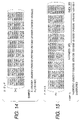
- FIG. 14 is a diagram showing a bit pattern as an example of a generator matrix of a (72, 64) code (correction Hamming code of one-bit correction and two-bit detection).
- FIG. 15 is a diagram showing a bit pattern as an example of a test matrix of a (72, 64) code (correction Hamming code of one-bit correction and two-bit detection).
- FIG. 16 is a schematic circuit diagram showing an example of an ECC circuit used for the invention.
- FIG. 17 is a schematic circuit diagram showing an example of an encoder of a cyclic Hamming code having a length of 255 bits used for the invention.
- FIG. 18 is a schematic circuit diagram showing an example of a coder of a cyclic Hamming code having a length of 255 bits used for the invention.
- FIG. 19 is a schematic circuit diagram showing an example of an ECC circuit (codec) of a cyclic Hamming code having a length of 255 bits used for the invention.
- FIG. 20 is a schematic circuit diagram showing an example of an ECC circuit of a cyclic Hamming code having a length of 32767 bits used for the invention.
- FIG. 21 is a timing chart showing an example of a refresh operation of an SDRAM according to the invention.
- FIG. 22 is a timing chart of a part for explaining a data storing-method of a dynamic RAM using the ECC circuit according to the invention.
- FIG. 23 is a timing chart of another part for explaining the data storing method of the dynamic RAM using the ECC circuit according to the invention.
- FIG. 24 is a timing chart of the rest for explaining the data storing method of the dynamic RAM using the ECC circuit according to the invention.
- FIG. 25 is a timing chart for explaining the data storing method of the dynamic RAM using the ECC circuit according to the invention.
- FIG. 26 is a timing chart for explaining the data storing method of the dynamic RAM using the ECC circuit according to the invention.
- FIG. 27 is a memory area use diagram of an example of the DRAM according to the invention.
- FIG. 28 is a memory area use diagram of another example of the DRAM according to the invention.
- FIG. 29 is a memory area use diagram of another example of the DRAM according to the invention.
- FIG. 30 is a memory area use diagram of another example of the DRAM according to the invention.
- FIG. 31 is a circuit diagram showing an example of a voltage setting circuit used for a cell leak monitor used for the invention.
- FIG. 32 is a circuit diagram showing an example of an oscillator using the cell leak monitor used for the invention.
- FIGS. 33A , 33 B, and 33 C are schematic diagrams of a carrier generating mechanism.
- FIG. 34 is an operation waveform chart of a basic OSC of an example of a cell leak monitoring method according to the invention.
- FIG. 35 is a waveform chart for explaining an internal power source control operation in a sleep mode (super low power mode) in the DRAM according to the invention.
- FIG. 36 is a circuit diagram showing an example of an internal step-down power source provided for the DRAM according to the invention.
- FIG. 1 is a general block diagram showing an example of a dynamic RAM (hereinbelow, simply called DRAM) according to the invention.
- the DRAM of the example is directed to an SDRAM (Synchronous Dynamic Random Access Memory).
- SDRAM Serial Dynamic Random Access Memory
- the SDRAM of the example has, but not limited, four memory arrays 200 A to 200 D in correspondence with four memory banks.
- the diagram illustrates two memory arrays 200 A and 200 D out of the four memory arrays 200 A to 200 D.
- Each of the memory arrays 200 A to 200 D corresponding to the four memory banks 0 to 3 has dynamic memory cells arranged in a matrix.
- a terminal for selecting memory cells arranged in the vertical direction of the memory array in the diagram is coupled to a word line (not shown), and data input/output terminals of memory cells arranged in the lateral direction are coupled to complementary data lines (not shown) every row.
- One of the not-shown word lines of the memory array 200 A is driven to a selection level in accordance with a decoding result of a row address signal by a row decoder 201 A.
- the row decoder 201 A includes a word driver for driving one of word lines to the selection level in accordance with a decoding result.
- the not-illustrated complementary data lines in the memory array 200 A are coupled to input/output lines (IO lines) via a sense amplifier 203 A, an IO gate 204 A as a column selection circuit, and a column decoder 205 A.
- the IO gate includes a main amplifier and a write amplifier.
- a sense amplifier 202 A is an amplifier for detecting and amplifying a very small potential difference appearing on each complementary data line when data is read from a memory cell.
- the I/O gate 204 A includes a switch MOSSFET for selecting one of the complementary data line so as to be coupled to a complementary I/O line.
- the column switch MOSFET performs a selecting operation in accordance with a result of decoding a column address signal by the column decoder 205 A.
- the not-illustrated memory arrays 200 B and 200 C are also similarly provided with row decoders 201 B and 201 C, sense amplifiers 203 B and 203 C, I/O gates 203 B and 203 C, and column decoders 205 B and 205 C, respectively.
- the I/O line is shared by the memory banks and is connected to the output terminal of a data input circuit (DIN buffer) 210 and an input terminal of a data output circuit (DOUT buffer) 211 .
- Terminals D 0 to D 7 are, although not limited, data input/output terminals for inputting or outputting data D 0 to D 7 of eight bits.
- Address signals A 0 to A 14 supplied from an address input terminal are held once in an address register 213 .
- a row address signal for selecting a memory cell is supplied to the row decoders 201 A to 201 D of the memory banks via a row address multiplexer 206 .
- a 13 and A 14 are designated and supplied to a bank control circuit 212 where selection signals for the four memory banks are generated.
- a column address signal is held in a column address counter 207 .
- a refresh counter 208 generates a row address in an automatic refresh mode and a row address and a column address in a self refresh mode.
- the DRAM has a storage capacity of 256 bits
- address signals from A 0 to A 10 are valid in the ⁇ 8 configuration.
- the column address signals which are time-sequentially input are supplied as preset data to the column address counter 208 .
- the column address signal as the preset data or a value obtained by sequentially incrementing the column address signal is output toward the column decoders 205 A to 205 D of the memory banks.
- a control logic 209 has a command decoder 2091 , a refresh controller 2092 , a mode register 2093 .
- the mode register 2093 holds various operation mode information. Only one of the row decoders 201 A to 201 D, which corresponds to the bank designated by the bank control circuit 212 operates and is allowed to perform a word line selecting operation.
- control logic 209 although not limited, external control signals such as a clock signal CLK, a clock enable signal CKE, a chip select signal /CS (the “/” designation indicates that the signal is active low), a column address strobe signal /CAS, a row address strobe signal /RAS, and a write enable signal /WE, DQM, and an address signal sent via the mode register 2093 are supplied.
- the control logic 209 generates an internal timing signal for controlling an operation mode of the SDRAM and the operation of the circuit block on the basis of a change in level, timing, and so on of the signals.
- the control logic 209 has an input buffer corresponding to each of the signals.
- the other external input signals are made significant synchronously with the rising edge of the internal clock signal.
- the chip select signal /CS instructs to start a command input cycle by its low level.
- the chip select signal /CS is at the high level (chip not-selected state)
- the other inputs are not significant.
- the memory bank selecting state which will be described hereinlater and the internal operation of a burst operation are not influenced by a change to the chip non-selection state.
- Each of the signals /RAS, /CAS, and /WE has a function different from that of a corresponding signal in a regular DRAM but becomes significant when a command cycle to be described hereinlater is defined.
- the clock enable signal CKE is a signal instructing validity of the following clock signal.
- the signal CKE is at the high level, the rising edge of the following clock signal CLK is valid.
- the signal CKE is at the low level, the rising edge of the following clock signal CLK is invalid.
- the signal /OE is also supplied to the control logic 209 .
- the signal /OE is, for example, at the high level, the data output circuit 211 enters a high output impedance state.
- the row address signal is defined by the level in the row address strobe and bank active command cycle to be described hereinlater, which is synchronized with the rising edge of the clock signal CLK (internal clock signal).
- the address signals A 13 and A 14 are regarded as bank selection signals in the row address strobe and bank active command cycle. Specifically, by the combination of the signals A 13 and A 14 , one of the four memory banks 0 to 3 is selected.
- the memory bank selecting control is performed by a process of, but not limited, activating only the row decoder on the selected memory bank side, selecting none of column switching circuits on the side of not-selected memory banks, connecting only the selected memory bank to the data input circuit 210 and the data output circuit 211 , and so on.
- an internal power source generating circuit which receives operation voltages such as VCC and VSS supplied from a power source terminal and generates various internal voltages such as an internal boosted voltage VPP corresponding to the selection level of a word line, an internal step-down voltage VDL corresponding to an operation voltage of the sense amplifier, and an internal step-down voltage VPERI corresponding to an operation voltage of a peripheral circuit and, in addition, although not shown, a memory cell plate voltage, a precharge voltage such as VDL/2, and a substrate back-bias voltage VBB.
- a cyclic code is used as a DRAM on-chip ECC. Though only in the self refresh mode, reduced standby current by correcting (masking) a refresh error is realized.
- ECC circuits (codecs) 214 A to 214 D are provided in correspondence with the memory banks 0 to 3 , respectively.
- the circuit scale of a coder/decoder (codec) as the ECC becomes smaller. Thus, a longer code length and the reduced parity bits can be achieved., and a disadvantage related to the area by the DRAM onchip ECC can be minimized.
- a plurality of cycles are necessary for generating a parity bit and correcting an error bit.
- the application range is therefore limited to a case where high access speed is not required such as a case where the SDRAM enters the self refresh mode for a data retention mode and a case where the SDRAM returns from the self refresh mode to a normal mode. Because of such limitation on the operation of the ECC, the power consumption can be largely reduced.
- a refresh pause error bit can be corrected, and the ECC circuits do not operate in the self refresh in a data retention mode. Therefore, even when an error bit occurs, it is left without being corrected in the self refresh period in the data retention mode.
- the ECC circuits 214 A to 214 D process 16 bits per time in accordance with a column access, output 16 parity bits each time (finally) at the time of coding, and sequentially output corrected data of 16 bits and an error position (column address of 10 bits) at the time of decoding.
- the I/O width seems to be eight bits, it is designed so as to be commonly used by the ⁇ 4, ⁇ 8, and ⁇ 16 configurations, so that the I/O width can be therefore enlarged to 16 bits.
- the column address has a nine-bit width. For an access to a parity area, the column address is internally increased to 10 bits.
- the operation procedure of the ECC circuits 214 A to 214 D is as follows.
- FIG. 2 is a general block diagram of another example of the DRAM according to the invention.
- the DRAM of the example only one ECC circuit is provided in the DRAM chip. That is, the ECC circuit is commonly used by the four memory banks.
- the operations of calculating and correcting a parity bit are performed by the control logic in the example of FIG. 1 , they are performed by the user in this case.
- the operating procedure by the ECC circuit 214 of the example is as follows. ⁇ circle around (1) ⁇ Before entering the self refresh mode for the data retention mode, the SDRAM enters a parity bit calculating mode (new mode). Specifically, the ECC circuit 214 is made active to enable the parity bit calculation and the writing operation for all the codes to be executed by the paging operation.
- FIG. 3 is a circuit diagram showing an example of a DRAM according to the invention.
- FIG. 3 illustrates a simplified circuit diagram of processes from address input till data output, mainly showing a sense amplifier portion.
- the example is directed to what is called a two-intersection architecture in which a pair of complementary bit lines are folded and extend in parallel with each other by using the sense amplifier as a center.
- a hierarchical structure such that word lines are constructed by a main word line MWL and a subword line SWL, and input/output lines are constructed by a local input/output line LIO and a main input/output line MIO.
- Circuits provided for a sense amplifier 16 and a cross area 18 sandwiched by two subarrays 15 are illustrated and the others are shown as blocks.
- MOS inherently stands for a metal oxide semiconductor.
- the MOS generally called in recent years includes a configuration in which a metal in the substantial portion of a semiconductor device is replaced by a non-metal electric conductor such as polysilicon or a configuration in which oxide is replaced by another insulating material.
- CMOS has also wider technical meaning according to a change in the definition of the MOS.
- MOSFET is also understood, not in a narrow sense but, in a broader sense, for example, to be substantially regarded as an insulating gate field effect transistor.
- the CMOS, MOSFET, and so on in a broader sense as described above are adopted.
- a dynamic memory cell positioned between the subword line SWL provided for the memory mat 15 and one (BL) of the complementary bit lines BL and BLB is illustrated as a representative.
- the dynamic memory cell has an address selection MOSFET Qm and a storage capacitor Cs.
- the gate of the address selection MOSFET Qm is connected to the subword line SWL, the drain of the MOSFET Qm is connected to the bit line BL, and the storage capacitor Cs is connected to the source.
- the other electrode of the storing capacitor Cs is commonly used and a plate voltage VPLT is applied to the electrode.
- a negative back bias voltage VBB is applied to the substrate (channel) of the MOSFET Qm.
- the back bias voltage VBB is set to a voltage like ⁇ 1V.
- the selection level of the subword line SWL is set to a high voltage VPP higher than the high level of the bit line only by the amount of a threshold voltage of the address selection MOSFET Qm.
- a high level amplified by the sense amplifier and given to a bit line is set to the internal voltage VDL level.
- the high voltage VPP corresponding to the selection level of the word line is equal to a sum of VDL+Vth+ ⁇ .
- the pair of complementary bit lines BL and BLB of the subarray provided on the left side of the sense amplifier are disposed parallel to each other as shown in FIG. 3 .
- the complementary bit lines BL and BLB are connected to input/output nodes of a unit circuit of the sense amplifier by shared switch MOSFETs Q 1 and Q 2 , respectively.
- the unit circuit of the sense amplifier takes the form of a CMOS latch circuit having N-channel type amplification MOSFETs Q 5 and Q 6 and P-channel type amplification MOSFETs Q 7 and Q 8 having gates and drains connected so as to cross with each other in a latch form.
- the sources of the N-channel type MOSFETs Q 5 and Q 6 are connected to a common source line CSN.
- the sources of the P-channel type MOSFETs Q 7 and Q 8 are connected to a common source line CSP.
- a power switch MOSFET is connected to each of the common source lines CSN and CSP.
- the common source line CSN to which the sources of the N-channel type amplification MOSFETs Q 5 and Q 6 are connected, an operation voltage corresponding to the ground potential is applied by an N-channel type power switch MOSFET Q 14 provided in the cross area 18 .
- the common source line CSP to which the sources of the P-channel type amplification MOSFETs Q 7 and Q 8 are connected is provided with an N-channel type power MOSFET Q 15 for supplying the internal voltage VDL.
- the power switch MOSFETs may be provided so as to be distributed to unit circuits.
- Sense amplifier activate signals SAN and SAP to be supplied to the gates of the N-channel type power MOSFETs Q 14 and Q 15 are signals of the same phase which are set to the high level when the sense amplifier is made active.
- the high level of the signal SAP is equal to the boosted voltage VPP level.
- the boosted voltage VPP is about 3.6V when VDL is 1.8V. Consequently, after setting the N-channel type MOSFET Q 15 in an ON state, the common source line CSP can be set to the internal voltage VDL level.
- a precharge (equalize) circuit constructed by an equalize MOSFET Q 11 for short-circuiting the complementary bit lines and switch MOSFETs Q 9 and Q 10 for supplying the half precharge voltage VBLR to a complementary bit line.
- a precharge signal PCB is supplied commonly to the gates of the MOSFETs Q 9 to Q 11 .
- a driver circuit for generating the precharge signal PCB has an inverter circuit (not shown) in the cross area to make the rising and fall edges occur at high speed. More specifically, when a memory access is started, prior to a word line selecting timing, the MOSFETs Q 9 to Q 11 constructing the precharge circuit are switched at high speed through the inverter circuits provided so as to be distributed to the cross areas.
- an IO switch circuit IOSW (constructed by switch MOSFETs Q 19 and Q 20 for connecting the local input/output lines LIO and the main input/output lines MIO) is disposed. Further, a half precharge circuit of the common source lines CSP and CSN of the sense amplifier, a half precharge circuit of the local input/output lines LIO, a VDL precharge circuit of the main input/output lines, a distributed driver circuit of shared selection signal lines SHR and SHL, and the like are also provided.
- the unit circuit of the sense amplifier is connected via shared switch MOSFETs Q 3 and Q 4 to the similar complementary bit lines BL and BLB in the subarray 15 on the lower side of the drawing. For example, when the subword line SWL in the upper subarray is selected, the upper shared switch MOSFETs Q 1 and Q 2 in the sense amplifier are turned on and the lower shared switch MOSFETs Q 3 and Q 4 are turned off. Switch MOSFETs Q 12 and Q 13 construct a column (Y) switch circuit.
- the column switch circuit When the selection signal YS is set to the selection level (high level), the column switch circuit is turned on to thereby connect the input/output nodes of the unit circuit of the sense amplifier with local input/output lines LIO 1 , LIO 1 B, LI 02 , LI 02 B, and so on.
- the input/output nodes of the sense amplifier are connected to the complementary bit lines BL and BLB on the upper side, a weak signal of a memory cell connected to the selected subword line SWL is amplified, and the amplified signal is transmitted to the local input/output lines LIO 1 and LIO 1 B via the column switch circuit (Q 12 and Q 13 ).
- the local input/output lines LIO 1 and LIO 1 B extend along the sense amplifier column, that is, in the lateral direction of the drawing.
- the local input/output lines LIO 1 and LIO 1 B are connected to the main input/output lines MIO and MIOB to which input terminals of a main amplifier 61 are connected, via the IO switch circuit constructed by the N-channel type MOSFETs Q 19 and Q 20 provided in the cross area 18 .
- the IO switch circuit is switched by a selection signal obtained by decoding an X address signal.
- the IO switch circuit may have a CMOS switch configuration in which a P-channel type MOSFET is connected in parallel with each of the N-channel type MOSFETs Q 19 and Q 20 .
- the column selection signal YS is switched by a counter operation, and the connection between the local input/output lines LIO 1 and LI 01 B and LI 02 and LIO 2 B and two pairs of complementary bit lines BL and BLB of the subarray is sequentially switched.
- An address signal Ai is supplied to an address buffer 51 .
- the address buffer 51 operates in a time sharing manner to capture an X address signal and a Y address signal.
- the X address signal is supplied to a predecoder 52 , and a signal for selecting the main word line MWL is generated via a main row decoder 11 and a main word driver 12 .
- the address buffer 51 receives the address signal Ai supplied from an external terminal, and is operated by the source voltage VDD (or VCC) supplied from the external terminal.
- the predecoder 52 is operated by the step-down voltage VPERI obtained by dropping the source voltage VDD, and the main word driver 12 is operated by the boosted voltage VPP.
- a column decoder (driver) 53 includes a driving circuit for generating an operation voltage by a MOSFET Q 23 as a component of the VCLP generating circuit, receives the Y address supplied by the time-sharing operation of the address buffer 51 , and generates the selection signal YS.
- the main amplifier 61 is operated by the step-down voltage VPERI and outputs an amplified signal from an external terminal Dout via an output buffer 62 operated by the source voltage VDD supplied from an external terminal.
- a write signal input from an external terminal Din is captured via an input buffer 63 and is supplied to the main input/output lines MIO and MIOB via a write amplifier (write driver) included in the main amplifier 61 in the diagram.
- a level shifter and a logical unit for outputting an output signal of the level shifter synchronously with a timing signal corresponding to the clock signal are provided.
- the source voltage VDD supplied from the external is set to 3.3V
- the step-down voltage VPERI supplied to an internal circuit is set to 2.5V
- the operation voltage VDL of the sense amplifier is set to 1.8V.
- the word line selection signal (boosted voltage) is set to 3.6V.
- the bit line precharge voltage VBLR is set to 0.9V corresponding to VDL/2
- the plate voltage VPLT is also set to 0.9V.
- the substrate voltage VBB is set to ⁇ 1.0V.
- the source voltage VDD supplied from the external terminal may be set to a low voltage such as 2.5V. When the source voltage VDD is low, each of the step-down voltages VPERI and VDL may be similarly set to about 1.8V.
- the source voltage VDD supplied from the external terminal is set to 3.3V, and each of the step-down voltage VPERI supplied to the internal circuit and the sense amplifier operation voltage VDL may be set to 2.0V or 1.8V.
- the internal voltages can be varied with respect to the external source voltage VDD.
- FIG. 4 is a characteristic diagram for explaining the relation between the refresh cycle of the DRAM and the standby current.
- the refresh cycle of the SDRAM under present conditions is about 80 ms in accordance with a data retaining characteristic of a trail bit.
- the current consumption in the refresh operation in such a cycle is about 511 ⁇ A (1 mA in the standard) which is relatively high.
- an error in the trail bit can be covered by the correctability of the ECC circuit by the application of the invention. Consequently, the refresh cycle can be made long like about 1 second or longer in accordance with the data retaining capability of other memory cells ignoring the error.
- the ECC circuit does not operate in the self refresh period, the current consumption can be largely reduced to about 87 ⁇ A (100 ⁇ A in the standard).
- the refresh cycle of about 1 second includes a margin of the worst case of the data retention time at high temperature.
- the data retention time of a memory cell at room temperature is longer than that at high temperature by about 10 seconds.
- the invention will be more concretely described hereinbelow.
- the concrete configuration and the operation of the ECC circuit will be described.
- the configuration of a long cycle OSC, an example of improving desired temperature dependency by combining the ECC circuit, and a case of combining a sleep mode (in which the internal power source is stopped) to further reduce the standby current will be described.
- a new command to improve the usability of the DRAM is added. Specifically, as shown in the truth table of FIG. 5 , in an SDRAM of 256 Mbits, address signals A 8 to A 12 , BA 0 and BA 1 are used. In an SDRAM of 64 Mbits, address signals A 8 to A 13 are used. In addition to the write mode as in the conventional SDRAM, a super low-power mode is used.
- An added operation code (OPCODE # 10 ) relates to the sleep mode in which the internal power source that determines the standby current is stopped. At this time, the standby current reaches about 2 ⁇ A.
- the stop/start of the sleep mode will be described hereinlater with reference to FIGS. 35 and 36 .
- the basic OSC oscillator
- the “#” designation indicates that the numeral is hexadecimal.
- the added operation code (OPCODE # 20 ) relates to the cell-leak monitor mode in which the basic OSC (OSC used in the self refresh mode) is switched to a cell leak monitor. A similar operation is performed in the sleep mode.
- the added operation code (OPCODE # 11 ) relates to an ECC syndrome mode in which the ECC circuit is activated.
- Data read by a read command and sent to an I/O is mechanically captured and subjected to syndrome calculation.
- a signal S goes high (H level)
- data is captured by a read command, and cyclic shifting of a shift register is performed.
- 64 information bits are sequentially captured, eight parity bits remain in the shift register and a code having a length of 72 bits is resulted.
- syndrome calculation pre-process of decoding
- the added operation code (OPCODE # 21 ) relates to an ECC parity mode in which the ECC circuit is activated.
- the contents of the shift register are sequentially output to the I/O bus and written to a designated address.
- masking with a data mask signal DQM is required.
- the command is recognized as a normal write command, and data is captured from the I/O buffer (DQ pin) and written to the designated address.
- the data mask signal is used to write a parity bit (check bit) into a memory cell after parity calculation by the operation code (OPCODE # 11 ).
- a signal P of the ECC circuit of FIG. 19 goes high (H level) and only cyclic shift of the shift register is performed in response to the write command. Since the signal S is at the L (low) level in this case, “0” is sent to the shift register, and the data in the shift register is sequentially output bit by bit to the I/O bus.
- the added operation code (OPCODE # 31 ) relates to an ECC correct mode in which the ECC circuit is activated. According to a syndrome pattern resulted in the shift register, read data is corrected one by one after the syndrome calculation by the OPCODE # 11 . Concretely, for example, a signal C of the ECC circuit of FIG. 19 goes high (H level).
- a process of correcting data of the I/O bus on the basis of the remained values in the shift register, and the cyclic shift of the shift register are mechanically executed.
- inverted data is output to the I/O buss.
- the data is output as it is.
- the corrected data is written in the designated address. In this case, in a manner similar to the ECC parity mode, masking with the data mask signal DQM is necessary. When the masking with the signal DQM is not made, the command is recognized as a normal write command.
- the refresh cycle dependency is eliminated by masking the tail bits by the ECC circuit and reducing the DC in the sleep mode by using both the long cycle OSC by the cell leak monitor and the long cycle in the cell-leak monitor, so that a super low power such as 10 ⁇ A (3.7 ⁇ A in the drawing) can be achieved.
- a super low power is comparable to a low-power SRAM (static RAM).
- FIG. 6 is a state transition diagram of the basic OSC.
- a relatively short refresh cycle is set by an oscillator by a delay circuit using an RC time constant. (RC-Delay).
- a sleep mode (cell-leak monitor mode)
- a relatively long refresh cycle is set by using the cell leak monitor.
- FIG. 7 is a state transition diagram of an internal power source.
- the supply capability of the internal power source is controlled in three levels of “full active”, “active”, and “standby”.
- “Drowsy” is a state where the power is on (the internal power circuit operates) only when a refresh operation is performed by the basic OSC of FIG. 6 .
- “Stop” indicates a state where the power source is completely stopped except for a power source which cannot be stopped.
- FIG. 8 is a pause refresh characteristic diagram.
- the lateral axis denotes pause time and the vertical axis denotes normalized cumulative fail bits.
- a major distribution called normal bits and a minor distribution called tail bits exist.
- the pause of the refresh of each bit is determined by a junction leak which is parasitic on a storage node and varies in about three digits.
- the percentage of tail bits is about 0.0037%. In the case of 64 Mbits, the number of tail bits is about 25 Kbits.
- the pause of bits of more than 90% is 10 seconds or longer, the refresh cycle cannot be increased due to the small amount of tail bits. This characteristic including the number of tail bits is typical.
- FIG. 9 shows a refresh pause characteristic when the ECC circuit according to the invention is applied.
- the tail bit can be masked with a double-error correcting code having a length of 2K and the refresh cycle can be extended to one second or longer.
- the refresh cycle is at most 80 ms or so.
- a chip having a refresh cycle of 300 ms (L version) can be selected.
- FIG. 10 is a characteristic diagram for explaining the temperature dependency of the refresh pause characteristic.
- the refresh pause characteristic largely depends on the temperature.
- the refresh cycle is extended in digits at the temperature becomes lower. Since the temperature dependency (activation energy) of a tail bit is twice as large as that of a normal bit, the lower the temperature becomes, the difference becomes wider. Specifically, only by changing the refresh cycle in the self refresh mode in accordance with the temperature, large reduction in current consumption can be effectively realized. When the tail bit can be masked with the ECC circuit, the effect is further increased. Paying attention to this fact, in the invention, the cell leak monitor as a temperature monitor which will be described hereinlater is useful.
- FIG. 11 is a characteristic diagram of temperature dependency of the refresh pause characteristic.
- the lateral axis denotes the inverse of ambient temperature, and the vertical axis denotes the worst values of tail bits and normal bits.
- the temperature dependency (activation energy) of a normal bit is twice as large as that of a tail bit.
- the activation energy of the tail bit is about 0.35 eV and that of the normal bit is about 0.7 eV. Those are general values. It is considered that the difference between the tail bit and the normal bit is due to different carrier generating mechanisms.
- FIGS. 33A , 33 B, and 33 C are schematic diagrams for explaining the carrier generating mechanisms.
- an SRH current recombination current
- the activation energy of the diffused component is up to 1 eV.
- the activation energy further decreases and the current increases incomparably.
- the activation energy is about 0.35 eV in reality.
- the multiple trap here denotes a plurality of trap levels generated by a single failure. It is known that Cu (copper), Fe (iron), and the like in silicon (Si) generate a plurality of defect levels. According to the number of failures and levels of each bit, the junction leak current varies incomparably. Consequently, it is considered that the bits are very various as shown in FIG. 8 . However, this point has not been fully clarified.
- the adaptation refresh denotes a method of providing a laser fuse circuit (ROM) for each word line and performing a control of setting a short refresh cycle for a word line including a tail bit and setting a long refresh cycle for a word line including no tail bit in a self refresh mode.
- ROM laser fuse circuit
- the refresh cycle has to be set to the optimum value so that the standby current is set to the lowest value.
- the pause tail bit (the probability of occurrence of 0.0037%) exists in most word lines (16 Kbits in the case of 64 Mbits and 128 Kbits in the case of the main word line in the hierarchical word line system). Consequently, the refresh cycle can be seemingly improved from 80 ms to only about 350 ms. This is similar to the case where an enormous amount of row (X) repair bits are provided to repair pause fails.
- the VRT denotes refresh pause time which varies according to bits.
- the VRT is not special.
- the refresh pause is (to be strict) not always constant in all bits but varies during use of long time.
- bits for example, a bit which fluctuates only once in a few years and a bit which fluctuates once every few seconds (bit which fluctuates each time it is measured). Although a bit which fluctuates in a few seconds rarely appears, a bit which fluctuates once in a few years exists in most chips.
- a fluctuation bit is recognized by measuring fluctuation in refresh pause in each of bits before and after long-time reliability test. Most of the bits fluctuate between two determined values of a value (for example 11 seconds) of a normal bit in a better case and a value (for example, 220 ms) of a tail bit in the worse case.
- a bit of which data retaining time fluctuates as described above may be called a comet bit.
- a junction leak current which determines a refresh pause is a current having a failure as shown in FIGS. 33A to 33C . It can be considered that retention time becomes variable since the trap level appears or disappears for some reason. For example, many dangling bonds existing in the interface of an SiO2 (silicon oxide) film are terminated by H (hydrogen atoms). When the device is used for long time and an energy exceeding the bonding energy is applied, H (hydrogen atoms) are uncoupled and the trap level appears suddenly. On the other hand, H (hydrogen atoms) are floating in Si (silicon). The dangling bond is terminated sometime and the trap level disappears suddenly.
- an energy exceeding the bonding energy is applied in a post process before the device is used.
- the refresh cycle is made longer by repairing (including adaptation refresh)
- a bit of which refresh pause fluctuates appears some time during a long time use, which becomes an error bit.
- the repairing process is performed in a P test process in a wafer state before a completed product is used. Consequently, a large thermal stress is applied in post processes (such as assembly), and many bits become faulty at a stage of evaluating an assembly. It can be therefore said that, in principle, only the ECC circuit can mask the tail bits of the pause and extend the refresh cycle.
- the refresh cycle can be extended.
- the temperature dependency of the tail bit and that of a normal bit are largely different from each other.
- the temperature dependency (activation energy) of a normal bit is twice as large as that of a tail bit.
- the probability of occurrence of a tail bit is 0.01% or less. Consequently, the tail bit cannot be monitored, in other words, a leak source corresponding to the tail bit cannot be formed stably.
- a cell leak monitor in which the characteristics of a normal bit are reflected can be used. In a combination of the cell leak monitor in which the characteristics of a normal bit are reflected and the ECC circuit, the refresh cycle can be extended.
- FIG. 12 is a characteristic diagram for explaining a pause fail bit correctability of a t-error-correcting code (BSH code).
- BSH code t-error-correcting code
- FIG. 13 is a characteristic diagram for explaining the relation between an information bit length (k) of the t-error-correcting code (BCH code) and parity bits (n-k).
- k information bit length
- n-k parity bits
- k information bit length
- n-k parity bits
- a value is a threshold of the size of a parity area to be added
- the BCH code of the quadruple-error-correction code having a length of 4K (53 parity bits/4K) or the double-error-correcting code having a length of 2K (24 parity bits/2K) satisfies the condition.
- FIGS. 14 and 15 are bit pattern diagrams showing an example of a generator matrix and a check matrix of a (72, 64) code (correction Hamming code for one-bit correction and two-bit detection).
- an (8 ⁇ 8) matrix is cyclically, repeatedly provided.
- the check matrix is obtained only by adding a unit matrix. In such a configuration, it is sufficient to provide a circuit of calculating the (8 ⁇ 8) matrix and to repreatedly execute the calculation, so that the circuit scale can be reduced.
- X denotes a transmission language
- Y a reception language
- P a check bit
- S a syndrome
- G generator matrix
- H H a check matrix.
- FIG. 14 shows a parity bit calculation example
- FIG. 15 is a syndrome calculation example. It is understood that the calculations are almost the same in the examples.
- matrix calculation is executed while including the parity bit. Since the syndrome and an error position correspond to each other in a one-to-one manner, it is sufficient to correct an error (to perform a data inverting process) by a syndrome decoder.
- FIG. 16 is a schematic circuit diagram of an example of an ECC circuit used for the invention.
- the example corresponds to those of FIGS. 14 and 15 , and is directed to an ECC code (codec) of a correction Hamming code (72, 64).
- codec code of a correction Hamming code (72, 64).
- REG 1 denotes a column address latch
- REG 2 denotes a data input register
- REG 3 indicates a data output register.
- a signal S 1 goes high (H level).
- a signal S 2 goes high (H level).
- a signal P goes high (H level). All of shift resistors (eight bits) are output to the data output register REG 3 .
- a signal C goes high (H level). Corrected data is output to the data output register REG 3 via an I/O bus by the syndrome decoder.
- the syndrome decoder In the correcting operation, the syndrome decoder outputs a Y address of error data in accordance with a syndrome pattern.
- the data is read by a read command. Since the error position (one of the eight bits) is already set to the H (high) level, the corrected data is output to the I/O bus, captured by the data output register REG, and corrected data is rewritten to a memory array by a write command.
- FIG. 18 is a schematic circuit diagram of an example of a decoder of a cyclic Hamming code having a length of 255 bits used in the invention.
- One decoder (one circuit) is provided for each bit of the I/O bus. When the I/O bus has the ⁇ 4 configuration, four circuits are provided. When the I/O bus has the ⁇ 8 configuration, eight circuits are provided. In the case of using one device (circuit), it is sufficient to provide a parallel-to-serial converter between the I/O bus and the circuit.
- the signal S in the ECC syndrome mode, is set to the H (high) level.
- the signal C In the ECC correct mode, the signal C is set to the H level.
- the address space is enlarged to the parity bit area in a manner similar to the example of FIG. 16 .
- FIG. 17 is a schematic circuit diagram of an example of an encoder of a cyclic Hamming code having a length of 255 bits used in the invention.
- one encoder one circuit is provided for each bit of the I/O bus.
- the I/O bus has the ⁇ 4 configuration, four circuits are provided.
- the I/O bus has the ⁇ 8 configuration, eight circuits are provided.
- the signal S in the ECC syndrome mode, is set to the H (high) level.
- the signal P In the ECC parity mode, the signal P is set to the H level.
- the address space is enlarged to the parity bit area in a manner similar to the example of FIG. 16 .
- FIG. 19 is a schematic circuit diagram of an example of an ECC circuit (codec) of a cyclic Hamming code having a length of 255 bits used in the invention.
- one encoder one circuit is provided for each bit of the I/O bus.
- the I/O bus has the ⁇ 4 configuration, four circuits are provided.
- the I/O bus has the ⁇ 8 configuration, eight circuits are provided.
- the encoder and the decoder have almost the same configuration and can be commonly used as shown in FIG. 19 .
- the signal S in the ECC syndrome mode, is set to the H (high) level.
- the signal P In the ECC parity mode, the signal P is set to the H level.
- the signal C In the ECC correct mode, the signal C is set to the H level.
- the address space is enlarged to the parity bit area in a manner similar to the example of FIG. 16 .
- the code length can be shortened.
- the code length of the circuit of FIG. 16 can be increased to 255 bits at the maximum. For example, when 64 information bits are captured, a code of 72 bits (parity 8 bits) is encoded. When 64 information bits and eight parity bits are captured, a code of 72 bits is decoded. In such a manner, the circuit has the function equivalent to the (72, 64) code shown in FIG. 16 .
- the circuit system not only the circuit scale can be largely reduced but also the correctability can be freely changed by changing the code length (in a state where the number of parity bits is fixed to eight).
- BCH code t-error-correcting code
- a basic circuit configuration is the same. For simplicity, the case of the cyclic Hamming code is explained.
- FIG. 20 is a schematic circuit diagram of an example of an ECC circuit of a cyclic Hamming code having a length of 32767 bits used in the invention.
- the generator conforms to the recommendation of CCITT (Comotti Consultatif International de Telecommunicationphonie et de Télégraphie).
- the circuit can be freely adapted to the 4 ⁇ and 2K configurations, and the parity bits can be also saved (16 parity bits are fixed).
- a fire code can be used as a valid cyclic code other than the ECC used in the invention.
- the fire code can be generated by using a similar circuit configuration, and a burst error can be corrected. Specifically, even when a bit line error or a word line error which cannot be detected in a normal test appears in a pause test, it can be corrected. However, the number of parity bits is larger as compared with the Hamming code. Since a pause error bit, particularly, a tail bit is a physical one fail, the pause error is a unidirectional error.
- t-EC/AUDE code t-error-correcting code/all-unidirectional-error-detecting code
- the fire code is disclosed by Fire P., “A Class of Multiple-Error-Correcting Codes for Non-Independent Errors”, Sylvania Report RSL-E-1., Sylvania Electric Defense Lab. Mountain View, Calif. (1959).
- the Berger code is disclosed by Berger J. M., “A Note on Error-Detecting Codes for Asymmetric Channels”, Inform. and Control, Vol. 4, pp. 68 to 73 (1961).
- FIG. 21 is a timing chart of an example of a refresh operation of the SDRAM according to the invention.
- the self refresh mode is started, and (3) the SDRAM enters a self refresh mode.
- the self refresh mode is finished, and (5) all the bits are refreshed as a post process, thereby returning to the normal operation mode.
- the function is useful when the SDRAM is mounted on a conventional memory system.
- FIGS. 22 to 24 are timing charts for explaining the data storing method of the dynamic RAM using the ECC circuit according to the invention.
- the invention is applied to an SDRAM (having the ⁇ 4 configuration) of 256 Mbits.
- the cyclic hamming code (72, 64 code) of FIG. 19 is constructed in the Y direction, and the parity bit is increased in the Y direction (refer to FIG. 27 ).
- the cell leak monitor is started to finish the preceding process and to start the self refresh mode.
- a self refresh is carried out in the super low power mode (4).
- the refresh cycle in the super low power mode is controlled by the cell leak monitor and is set to be a long cycle of about 10 seconds at room temperature.
- a concentrated refresh is performed. During a period from the end of the refresh on all the bits until the start of the next concentrated refresh, the powers of unnecessary internal circuits are interrupted.
- an error occurs in a tail bit but is left as it is.
- the ECC syndrome mode (2) is started.
- a power-on time tPON is set, and a power supply operation time necessary for the internal circuits to perform normal operation is provided.
- the self refresh in which the refresh cycle is set to about 1 second (or longer) and the cell leak monitor is not used is carried out in place of the super low power mode, the powers of the internal circuits are untouched. It is consequently unnecessary to set the power-on time tPON.
- the SDRAM After elapse of the power-on time tPON, 72 bits are read by the read command, and the SDRAM enters the ECC correct mode (5).
- the ECC correct mode (5) the error of the tail bit is corrected by the read and write commands and errors in all the tail bits are corrected in such a manner.
- a distributed refresh is properly inserted.
- FIG. 24 after completing the post process, a normal operation can be performed.
- FIG. 25 is a timing chart for explaining the data storing method of the dynamic RAM using the ECC circuit according to the invention.
- the invention is applied to an SDRAM (having the ⁇ 4 configuration) of 256 Mbits.
- the cyclic Hamming code (72, 64 code) of FIG. 19 is constructed in the X direction and the parity bits are increased in the X direction (refer to FIG. 28 ).
- data may be captured to the ECC circuit by an X scan.
- the procedure is quite the same as that of FIGS. 22 to 24 .
- the X scan refresh is naturally conducted, so that the distributed refresh to prevent data from being destroyed in the pause time while all bits are encoded or decoded is unnecessary.
- the invention is applied to the SDRAM (having the ⁇ 4 configuration) of 256 Mbits.
- a memory chip is designed so as to be adapted to the ⁇ 4, ⁇ 8, and ⁇ 16 configurations. Consequently, in any of the word organizations, the memory chip can be adapted to all of the cases when the ⁇ 4 configuration is used in three modes of the ECC syndrome mode, ECC parity mode, and ECC correct mode. With the configuration, the ECC circuit to be mounted does not have to be changed according to the word organization and DQ pins do not become insufficient.
- FIG. 26 is a timing chart for explaining the data storing method of a dynamic RAM using the ECC circuit according to the invention.
- the invention is applied to an SDRAM (having the ⁇ 8 configuration) of 256 Mbits.
- the correction Hamming code 72, 64 code
- the parity bits are increased in the Y direction (refer to FIG. 27 ).
- a procedure is substantially the same as the example of FIGS. 22 to 24 .
- the ECC circuit (one) of the example processes eight bits in one cycle, the following points are different. (1) 64-bit data is read in eight cycles, while 64 cycles are necessary in the example of FIGS. 22 to 24 . (2) Even when a Y address is input in the ECC correct mode, it is invalid. A process is performed in two cycles of read and write cycles.
- FIG. 27 is a memory area use diagram of an example of the DRAM according to the invention.
- the check bit areas is increased in the Y direction in correspondence with the example of FIGS. 22 to 24 .
- FIG. 28 is a memory area use diagram of another example of the DRAM according to the invention.
- the check bit area is increased in the X direction in correspondence with the example of FIG. 25 .
- FIG. 29 is a memory area use diagram of another example of the DRAM according to the invention.
- the check bits are increased in the Y direction.
- the example corresponds to the example of FIG. 26 in which the process is performed on the eight-bit unit basis.
- FIG. 30 is a memory area use diagram of further another example of the SDRAM according to the invention.
- the invention is applied to a product code.
- the ECC circuit is directed to the configuration in which the cyclic Hamming codes, which are (2064, 2048) codes are provided in both the X and Y directions.
- the parity bits are increased in both X and Y directions. With only the Hamming code, only one bit can be corrected (minimum distance 3 ).
- the minimum distance becomes the product of two codes, that is, nine, so that the error correctability equivalent to the quadruple-error-correcting code having a length of 4 Kbits is obtained.
- the circuit scale is smaller and the number of parity bits is almost the same as compared with a quadruple-error-correcting BCH code.
- the number of cycles required for the ECC process increases.
- the standby time is sufficient longer than the ECC process time, it can be considered that there is no problem.
- a burst error such as a word line error or a bit line error can be also corrected.
- FIG. 31 is a circuit diagram showing an example of a voltage setting circuit used for a cell leak monitor employed in the invention.
- switch MOSFETs Q 10 to Q 18 and Q 20 to Q 27 each for short-circuiting a resistor in a series resistance circuit are provided and a switching control is performed by trimming signals TRM 1 ( 0 to 7 ) and TRM 2 ( 0 to 7 ).
- the trimming signals TRM 1 ( 0 to 7 ) and TRM 2 ( 0 to 7 ) are, but not limited, generated by blowing a fuse with a laser beam or the like.
- the number of resistors inserted between the source voltage VCC and the ground potential of the circuit is selected, a current flowing to the resistors is adjusted, gate-source voltages VP and VN of the P-channel type MOSFET Q 18 and the N-channel type MOSFET Q 28 are generated, and currents of a P-channel type current source MOSFET and an N-channel type current source MOSFET are set by a current mirror circuit.
- a voltage VR is a reference voltage for cell leak monitor, and a voltage VCELL is an input voltage written to a capacitor.
- FIG. 32 is a circuit diagram showing an example of an oscillator using the cell leak monitor used for the invention.
- a junction leak source is formed in a memory cell size. However, in the case of only one bit, as shown in FIG. 8 , the junction leak current varies in digits, so that it is difficult to make adjustment by using trimming means.
- the cell leak monitor at least 10 bits are connected in parallel so as to obtain a PN junction leak characteristic of around 50% fail.
- the cycle can be adjusted by the voltage VCELL (write voltage) and voltage VR (reference potential) in FIG. 31 , the number of cells to be connected, and parasite capacitance.
- the MOSFET Q 30 of a voltage comparing circuit is turned on to set an output signal OSC obtained via inverters N 30 and N 31 to the high level.
- the output signal is sent to a delay circuit via an AND gate which opens at the high level of a power-on signal PON to be described hereinlater, and a low-level signal is generated by an inverter N 32 .
- the low-level signal is boosted to a boosted voltage by a level shifter constructed by the MOSFETs Q 35 to Q 39 .
- the signal is sent to the gate of the switch MOSFET constructing a dummy cell to turn on the MOSFETs.
- the voltage VCELL is written in the capacitor C 30 .
- the signal OSC obtained via the voltage comparing circuit and the inverters N 30 and N 31 goes low, the output signal of the AND gate accordingly goes low, the output signal of the inverter N 32 goes high after delay time of the delay circuit, the output signal of the level shifter goes low, and the switch MOSFET is turned off. Consequently, the storage node of the capacitor C 30 enters a floating state, so that a charge holding state is set. The charge is discharged by a source-drain junction leak of the switch MOSFET in a manner similar to a memory cell.
- the cell leak monitor can be realized by masking a tail bit by using the ECC circuit.
- the temperature dependency of the tail bit and that of a normal bit are largely different from each other.
- the temperature dependency (activation energy) of a normal bit is twice as large as that of a tail bit.
- the probability of occurrence is 0.01% or less. Consequently, a leak source cannot be formed stably. Even if it is devised as shown in FIG. 32 , it does not mean anything for a tail bit.
- a cell leak monitor in which the characteristics of a normal bit are reflected can be used.
- the cell leak monitor becomes meaningful as a leak source.
- FIGS. 33A , 33 B, and 33 C are schematic diagrams of carrier generating mechanisms.
- FIG. 33C show a factor of dominance of the tail bit
- FIG. 33B show a factor of dominance of the normal bit.
- FIG. 34 is an operation waveform chart of a basic OCS as an example of a cell leak monitor method according to the invention.
- the refresh pulse OSC goes high, start-up of the internal source is instructed by an internal source start-up signal. After elapse of the time tPON set for the start-up, all bits are cencentratedly refreshed. Concurrently, the capacitor C 30 in the cell leak monitor as shown in FIG. 32 is charged up.
- a pulse SOSC 2 for concentrated refresh is generated by a ring oscillator using an RC time constant circuit separately provided or the like. After completion of the concentrated refresh, out of the internal sources, the source voltages of circuits which are not related to the data storing operation are interrupted by an internal source voltage stop signal.
- the oscillation signal OCS using the cell leak monitor as described above synchronously with the refresh cycle which is as long as about 10 seconds at a room temperature, the operations of start-up of the internal power source, concentrated refresh, and interruption of the internal power source are repeated.
- FIG. 35 is a waveform chart for explaining the internal power source controlling operation in the sleep mode (super low power mode) in the DRAM according to the invention.
- the example is characterized by the following two points. (1) The plate voltage VPLT is not dropped to prevent data from being destroyed by a plate bump. (2) The word line boosted voltage VPP is boosted after the power sources (VPERI and VDLA) of the word driver control circuit are started, and is dropped before the power sources (VPERI and VLDA) of the word driver control circuit are interrupted in order to prevent data from being destroyed by word line noise.
- the internal voltage VDLA is a voltage up to 1.8V of the internal step-down power source of a memory array and can be dropped.
- the internal voltage VDLB is a voltage up to 1.8V of the internal step-down power source of a peripheral circuit and cannot be dropped since it is used for the basic OCS or the like.
- VPERI 2 is a voltage which can be dropped, supplied to a peripheral circuit and is up to 2.4V.
- VPP is a voltage up to 3.4V
- VPERI is a voltage up to 2.4V
- a capacitance film (insulating film) is formed thinly, so that a margin on the withstand voltage and reliability of the capacitance film is narrow.
- the plate voltage VPLT is set to be equal to VSS, plate bump caused by stopping the power source does not occur.
- the reliability of the capacitance film decreases in digits (and the plate leak increases). Since doze in a recent device is high, the substrate effect is small. When a negative potential floats to 0V naturally, there is little harm.
- VBB to be equal to VSS as in the example, the power consumption is reduced.
- FIG. 36 is a circuit diagram of an example of the internal step-down power source provided for the DRAM according to the invention.
- the internal step-down power source serves as a voltage follower circuit for comparing the reference voltage VR and the output voltage VDL (VPERI) with each other and performing a control so that the voltages are equal to each other.
- the reference voltage VR is set to a desired voltage VDL or VPERI.
- the current source of a differential amplifier constructed by MOSFETs Q 44 to Q 49 is controlled by a signal ACT.
- the signal ACT is at the H level, the current source is made active to pass a relatively high current by the MOSFET Q 45 , thereby achieving high response.
- a DC current is largely consumed.
- the signal ACT is at the low level, the standby mode is set.
- the P-channel type MOSFET Q 51 as an output of the differential amplifier is made inactive to thereby set the sleep mode.
- the memory circuit any memory circuit may be used as long as it uses a dynamic memory cell as described above.
- the memory array portion may have what is called a single-intersection architecture or open bit line architecture in which complementary bit lines are extended on the right and left sides by using the sense amplifier as a center.
- the area for storing the parity bit may not be specially provided but a data area may be limited to assure an area for predetermined parity bits by software. Specifically, an area for parity bits is assured in correspondence with the built-in ECC circuit in advance.
- the ECC circuit is used by being activated. The case of using such a built-in ECC circuit is preferable for a small-scale system.
- the data storing method of the DRAM according to the invention as described above can be executed not only by using the ECC circuit built in the DRAM but also by software in a microcomputer system.
- a CPU itself enters a sleep mode
- data in the DRAM is read, a parity bit is generated by an ECC operation as described above and stored in the DRAM or SRAM, and a self refresh operation in a long cycle as described above is instructed.
- the CPU returns from the sleep mode, data of the DRAM and the corresponding parity bit are read, and an error of the DRAM, which occurs in the data retaining state is corrected.
- a function of managing the refresh by the CPU or the like may be added.
- the invention can be applied not only to the DRAM chip like an SDRAM but also a semiconductor integrated circuit device on which a DRAM is mounted like a system LSI.
- the invention can be widely used for the data storing method of the DRAM and the semiconductor integrated circuit device including the DRAM.
- a semiconductor integrated circuit device has: a memory circuit including a dynamic memory cell and having an information retaining mode during which data is not read/written from/to other circuits; and a data retention control circuit including an ECC circuit and a refresh cycle setting circuit.
- a memory circuit including a dynamic memory cell and having an information retaining mode during which data is not read/written from/to other circuits
- a data retention control circuit including an ECC circuit and a refresh cycle setting circuit.
Abstract
Description
- {circle around (1)} Before a refresh operation for the data retention mode, parity bits are calculated and written for all the codes (all bits) by the
ECC circuits 214A to 214D. A code is constructed by bits in the Y direction (on the same word line), and a parity bit is calculated and written while performing a paging operation. For example, a BCH code of 2048 bits (information bits) and 32 bits (parity bits) is generated. - {circle around (2)} A self refresh is executed in accordance with an OSC cycle. The refresh cycle is extended in the range of collectability. When the refresh cycle extended in the ECC correctable range is set, naturally, an error bit occurs in tail bits. In the data retention mode, an operation similar to the conventional self refresh is performed. That is, processes such as an error correcting process by the ECC circuit are not performed. The error correcting process by the ECC circuit may be periodically performed in predetermined cycles during the self refresh period. It is also possible to provide a temperature change detecting circuit for detecting whether a temperature change of the DRAM exceeds a predetermined value or not, and execute the error correcting process during the self refresh period in response to an instruction of the circuit. The self refresh cycle is initially set on the basis of refresh cycle information pre-stored in a memory circuit in a non-volatile manner.
- {circle around (3)} A process of correcting an error bit is performed before returning to the normal operation mode. Specifically, the ECC circuit is made active to calculate corrected data and an error position with respect to all the codes (all the bits) while performing the paging operation and to write the corrected data of the error bit. Such operations {circle around (1)} to {circle around (3)} are, different from those in the standard of a conventional self refresh mode, self refresh in a new mode (data retention mode) of a long period extended on the precondition that the error correcting process by the ECC circuit is performed. The long period may be adjusted (changed) by a refresh cycle changing circuit by a cell leak monitor or the like.
- {circle around (2)} The SDRAM enters the self refresh mode. In the self refresh {circle around (2)}, the OSC cycle is extended in the range of the correctability of the
ECC circuit 214. In a manner similar to the foregoing example, naturally, an error bit occurs in tail bits. In the data retention mode, an operation similar to the conventional self refresh is carried out. That is, processes such as the error correcting process by theECC circuit 214 are not performed. - {circle around (3)} Before the self refresh mode is canceled and the SDRAM returns to a normal operation, the SDRAM enters the data correcting mode (new mode). To be specific, the
ECC circuit 214 is made active to execute calculation of corrected data and error position (column address) and the correcting and writing operation of the corrected data for all the codes.
- (1) When a DRAM enters an operation mode for performing only an operation of retaining data, a check bit for error detection and correction is generated for plural data and stored, and a refresh operation is performed in a refresh cycle extended in a permissible range of error occurrence by an error correcting operation using the check bit. Before the DRAM returns to the normal operation from the data retaining operation, an error bit is corrected by using the data and the check bit, thereby enabling an error in a tail bit to be corrected. Thus, effects such that a long refresh cycle is achieved and, since no ECC operation is performed, the power consumption can be largely reduced are produced.
- (2) In addition, the plural data and the check bit are stored in a dynamic RAM, and the error detecting and correcting operation using the check bit is performed by a built-in error detecting and correcting circuit. Consequently, an effect such that the usability is increased is obtained.
- (3) A semiconductor integrated circuit device has: a memory circuit including a dynamic memory cell and having an information retaining mode during which data is not read/written from/to other circuits; and a data retention control circuit including an ECC circuit and a refresh cycle setting circuit. When the dynamic RAM enters an operation mode of performing only an operation of retaining data, for plural data, a check bit for error detection and correction is generated and stored by using the ECC circuit. The refresh cycle is extended by the refresh cycle setting circuit within a permissible range of error occurrence by an error correcting operation using the check bit. Before the DRAM returns from the information retaining mode to a normal operation mode, an error bit in data is corrected by using the data and the check bit by the ECC circuit, thereby enabling an error in a tail bit to be corrected. Thus, effects such that the long refresh cycle is achieved and, moreover, since no ECC operation is performed, the power consumption can be largely reduced are produced.
- (4) In addition, the check bit is stored in a memory cell included in the memory circuit. Consequently, an effect such that increased usability is achieved and the circuit is simplified is obtained.
- (5) In addition, the ECC circuit can correct two bits or more by using a cyclic code, allows data and a check bit to be stored in a memory cell read by an operation of selecting one of word lines in the memory circuit, and reads/writes data and check bits corresponding to the one word line. Thus, an effect such that the generation and storage of the check bit and the correction of the error bit can be performed at high speed with a simple configuration is produced.
Claims (7)
Priority Applications (2)
| Application Number | Priority Date | Filing Date | Title |
|---|---|---|---|
| US10/753,534 US7051260B2 (en) | 2000-08-14 | 2004-01-09 | Data storing method of dynamic RAM and semiconductor memory device |
| US11/399,485 US7318183B2 (en) | 2000-08-14 | 2006-04-07 | Data storing method of dynamic RAM and semiconductor memory device |
Applications Claiming Priority (4)
| Application Number | Priority Date | Filing Date | Title |
|---|---|---|---|
| JP2000245483A JP2002056671A (en) | 2000-08-14 | 2000-08-14 | Method for holding data for dynamic ram and semiconductor integrated circuit device |
| JP2000-245483 | 2000-08-14 | ||
| US09/923,405 US6697992B2 (en) | 2000-08-14 | 2001-08-08 | Data storing method of dynamic RAM and semiconductor memory device |
| US10/753,534 US7051260B2 (en) | 2000-08-14 | 2004-01-09 | Data storing method of dynamic RAM and semiconductor memory device |
Related Parent Applications (1)
| Application Number | Title | Priority Date | Filing Date |
|---|---|---|---|
| US09/923,405 Continuation US6697992B2 (en) | 2000-08-14 | 2001-08-08 | Data storing method of dynamic RAM and semiconductor memory device |
Related Child Applications (1)
| Application Number | Title | Priority Date | Filing Date |
|---|---|---|---|
| US11/399,485 Continuation US7318183B2 (en) | 2000-08-14 | 2006-04-07 | Data storing method of dynamic RAM and semiconductor memory device |
Publications (2)
| Publication Number | Publication Date |
|---|---|
| US20040148557A1 US20040148557A1 (en) | 2004-07-29 |
| US7051260B2 true US7051260B2 (en) | 2006-05-23 |
Family
ID=18735998
Family Applications (3)
| Application Number | Title | Priority Date | Filing Date |
|---|---|---|---|
| US09/923,405 Expired - Lifetime US6697992B2 (en) | 2000-08-14 | 2001-08-08 | Data storing method of dynamic RAM and semiconductor memory device |
| US10/753,534 Expired - Fee Related US7051260B2 (en) | 2000-08-14 | 2004-01-09 | Data storing method of dynamic RAM and semiconductor memory device |
| US11/399,485 Expired - Fee Related US7318183B2 (en) | 2000-08-14 | 2006-04-07 | Data storing method of dynamic RAM and semiconductor memory device |
Family Applications Before (1)
| Application Number | Title | Priority Date | Filing Date |
|---|---|---|---|
| US09/923,405 Expired - Lifetime US6697992B2 (en) | 2000-08-14 | 2001-08-08 | Data storing method of dynamic RAM and semiconductor memory device |
Family Applications After (1)
| Application Number | Title | Priority Date | Filing Date |
|---|---|---|---|
| US11/399,485 Expired - Fee Related US7318183B2 (en) | 2000-08-14 | 2006-04-07 | Data storing method of dynamic RAM and semiconductor memory device |
Country Status (4)
| Country | Link |
|---|---|
| US (3) | US6697992B2 (en) |
| JP (1) | JP2002056671A (en) |
| KR (1) | KR100795545B1 (en) |
| TW (1) | TW548648B (en) |
Cited By (17)
| Publication number | Priority date | Publication date | Assignee | Title |
|---|---|---|---|---|
| US20050281112A1 (en) * | 2004-06-18 | 2005-12-22 | Elpida Memory, Inc. | Semiconductor memory device and refresh period controlling method |
| US20060044914A1 (en) * | 2004-08-31 | 2006-03-02 | Sung-Ho Choi | Semiconductor memory devices in which the number of memory banks to be refreshed may be changed and methods of operating the same |
| US20060250867A1 (en) * | 2004-07-13 | 2006-11-09 | Headway Technologies, Inc. | Adaptive algorithim for MRAM manufacturing |
| US20080092016A1 (en) * | 2006-10-11 | 2008-04-17 | Micron Technology, Inc. | Memory system and method using partial ECC to achieve low power refresh and fast access to data |
| US20080109700A1 (en) * | 2006-11-03 | 2008-05-08 | Kwang-Jin Lee | Semiconductor memory device and data error detection and correction method of the same |
| US20080109705A1 (en) * | 2006-10-18 | 2008-05-08 | Pawlowski J Thomas | Memory system and method using ECC with flag bit to identify modified data |
| US20080222483A1 (en) * | 2007-03-08 | 2008-09-11 | Micron Technology, Inc. | Method, system, and apparatus for distributed decoding during prolonged refresh |
| US20090024884A1 (en) * | 2004-05-06 | 2009-01-22 | Micron Technology, Inc. | Memory controller method and system compensating for memory cell data losses |
| US20090189684A1 (en) * | 2008-01-30 | 2009-07-30 | Infineon Technologies Ag | Apparatus and Method for Waking up a Circuit |
| US20100034004A1 (en) * | 2008-08-07 | 2010-02-11 | Elpida Memory, Inc. | Semiconductor memory device of open bit line type |
| US20100054070A1 (en) * | 2004-07-15 | 2010-03-04 | Micron Technology, Inc. | Method and system for controlling refresh to avoid memory cell data losses |
| US20110289386A1 (en) * | 2009-06-24 | 2011-11-24 | Magic Technologies, Inc. | Method and apparatus for scrubbing accumulated data errors from a memory system |
| US20150100852A1 (en) * | 2013-10-07 | 2015-04-09 | Macronix International Co., Ltd. | Ecc method for double pattern flash memory |
| US9535785B2 (en) | 2014-01-17 | 2017-01-03 | Macronix International Co., Ltd. | ECC method for flash memory |
| CN107393596A (en) * | 2016-04-26 | 2017-11-24 | 三星电子株式会社 | Semiconductor memory apparatus and its method of operation |
| US10910035B2 (en) | 2018-12-03 | 2021-02-02 | Samsung Electronics Co., Ltd. | Dynamic semiconductor memory device and memory system with temperature sensor |
| US11429479B2 (en) * | 2020-07-16 | 2022-08-30 | Micron Technology, Inc. | Memory device activity-based copying defect management data |
Families Citing this family (116)
| Publication number | Priority date | Publication date | Assignee | Title |
|---|---|---|---|---|
| JP2003068076A (en) * | 2001-08-27 | 2003-03-07 | Elpida Memory Inc | Power control method for semiconductor memory, and semiconductor memory |
| US7051264B2 (en) * | 2001-11-14 | 2006-05-23 | Monolithic System Technology, Inc. | Error correcting memory and method of operating same |
| US7171605B2 (en) * | 2002-02-01 | 2007-01-30 | International Business Machines Corporation | Check bit free error correction for sleep mode data retention |
| GB2387089B (en) * | 2002-03-28 | 2004-12-22 | Matsushita Comm Ind Uk Ltd | Improved carryout word calculation for cyclic shift registers |
| US20030226090A1 (en) * | 2002-05-28 | 2003-12-04 | Thayer Larry Jay | System and method for preventing memory access errors |
| JP3914839B2 (en) * | 2002-07-11 | 2007-05-16 | エルピーダメモリ株式会社 | Semiconductor memory device |
| JP4282295B2 (en) | 2002-09-26 | 2009-06-17 | エルピーダメモリ株式会社 | Refresh counter and memory device |
| JP4205396B2 (en) | 2002-10-30 | 2009-01-07 | エルピーダメモリ株式会社 | Semiconductor integrated circuit device |
| DE10305008A1 (en) * | 2003-02-07 | 2004-08-19 | Robert Bosch Gmbh | Method and device for monitoring an electronic control |
| JP4381014B2 (en) * | 2003-03-18 | 2009-12-09 | 株式会社ルネサステクノロジ | Semiconductor integrated circuit |
| US6853591B2 (en) | 2003-03-31 | 2005-02-08 | Micron Technology, Inc. | Circuit and method for decreasing the required refresh rate of DRAM devices |
| JP4199591B2 (en) | 2003-05-16 | 2008-12-17 | エルピーダメモリ株式会社 | Cell leak monitoring circuit and monitoring method |
| KR100532448B1 (en) * | 2003-07-12 | 2005-11-30 | 삼성전자주식회사 | Memory controller capable of controlling refresh period of memory and method thereof |
| WO2005017914A1 (en) * | 2003-08-18 | 2005-02-24 | Fujitsu Limited | Semiconductor memory and operation method of semiconductor memory |
| JP4237038B2 (en) | 2003-12-01 | 2009-03-11 | エルピーダメモリ株式会社 | Semiconductor integrated circuit device |
| US7210077B2 (en) * | 2004-01-29 | 2007-04-24 | Hewlett-Packard Development Company, L.P. | System and method for configuring a solid-state storage device with error correction coding |
| JP4478974B2 (en) | 2004-01-30 | 2010-06-09 | エルピーダメモリ株式会社 | Semiconductor memory device and refresh control method thereof |
| JP4569182B2 (en) | 2004-03-19 | 2010-10-27 | ソニー株式会社 | Semiconductor device |
| JP4056488B2 (en) | 2004-03-30 | 2008-03-05 | エルピーダメモリ株式会社 | Semiconductor device testing method and manufacturing method |
| JP2006004560A (en) | 2004-06-18 | 2006-01-05 | Elpida Memory Inc | Semiconductor memory and its error correction method |
| JP2006004559A (en) | 2004-06-18 | 2006-01-05 | Elpida Memory Inc | Semiconductor storage device |
| JP4191100B2 (en) | 2004-06-18 | 2008-12-03 | エルピーダメモリ株式会社 | Semiconductor memory device |
| US20060010339A1 (en) * | 2004-06-24 | 2006-01-12 | Klein Dean A | Memory system and method having selective ECC during low power refresh |
| US7340668B2 (en) * | 2004-06-25 | 2008-03-04 | Micron Technology, Inc. | Low power cost-effective ECC memory system and method |
| US7151709B2 (en) * | 2004-08-16 | 2006-12-19 | Micron Technology, Inc. | Memory device and method having programmable address configurations |
| US7590918B2 (en) * | 2004-09-10 | 2009-09-15 | Ovonyx, Inc. | Using a phase change memory as a high volume memory |
| DE602004014371D1 (en) * | 2004-09-10 | 2008-07-24 | St Microelectronics Srl | Memory with built-in error correction code facility |
| US7392456B2 (en) * | 2004-11-23 | 2008-06-24 | Mosys, Inc. | Predictive error correction code generation facilitating high-speed byte-write in a semiconductor memory |
| US7644341B2 (en) * | 2004-12-30 | 2010-01-05 | Taiwan Semiconductor Manufacturing Co., Ltd. | Method and system for correcting soft errors in memory circuit |
| JP4802515B2 (en) * | 2005-03-01 | 2011-10-26 | 株式会社日立製作所 | Semiconductor device |
| JP4824936B2 (en) * | 2005-03-10 | 2011-11-30 | 株式会社日立製作所 | Inspection method for dynamic random access memory device |
| JP4643334B2 (en) | 2005-03-31 | 2011-03-02 | 富士通セミコンダクター株式会社 | Semiconductor memory device |
| US20060265636A1 (en) * | 2005-05-19 | 2006-11-23 | Klaus Hummler | Optimized testing of on-chip error correction circuit |
| US20060277359A1 (en) * | 2005-06-06 | 2006-12-07 | Faber Robert W | Blank memory location detection mechanism |
| US7382673B2 (en) * | 2005-06-15 | 2008-06-03 | Infineon Technologies Ag | Memory having parity generation circuit |
| US20070011596A1 (en) * | 2005-06-22 | 2007-01-11 | Jungwon Suh | Parity check circuit to improve quality of memory device |
| US7761773B2 (en) * | 2005-06-30 | 2010-07-20 | Sigmatel, Inc. | Semiconductor device including a unique identifier and error correction code |
| KR100615580B1 (en) * | 2005-07-05 | 2006-08-25 | 삼성전자주식회사 | Semiconductor memory device and data input and output method of the same, and memory system comprising the same |
| US7747933B2 (en) * | 2005-07-21 | 2010-06-29 | Micron Technology, Inc. | Method and apparatus for detecting communication errors on a bus |
| JP4547313B2 (en) * | 2005-08-01 | 2010-09-22 | 株式会社日立製作所 | Semiconductor memory device |
| KR100669352B1 (en) * | 2005-09-07 | 2007-01-16 | 삼성전자주식회사 | Nand flash memory device performing error detection and data reloading operation during copy back program operation |
| JP4745169B2 (en) * | 2005-09-16 | 2011-08-10 | 株式会社東芝 | Semiconductor memory device |
| JP4768374B2 (en) | 2005-09-16 | 2011-09-07 | 株式会社東芝 | Semiconductor memory device |
| KR100714487B1 (en) | 2005-11-29 | 2007-05-07 | 삼성전자주식회사 | Dynamic random access memory and a refresh cycle settlement method for the same |
| US7894282B2 (en) * | 2005-11-29 | 2011-02-22 | Samsung Electronics Co., Ltd. | Dynamic random access memory device and method of determining refresh cycle thereof |
| JP4575288B2 (en) * | 2005-12-05 | 2010-11-04 | 株式会社東芝 | Storage medium, storage medium playback apparatus, storage medium playback method, and storage medium playback program |
| WO2007076522A2 (en) * | 2005-12-28 | 2007-07-05 | Ethicon, Incorporated | Treatment of peripheral vascular disease using postpartum-derived cells |
| KR20070076849A (en) * | 2006-01-20 | 2007-07-25 | 삼성전자주식회사 | Apparatus and method for accomplishing copy-back operation in memory card |
| JP2007265557A (en) | 2006-03-29 | 2007-10-11 | Toshiba Corp | Semiconductor memory device |
| KR100810060B1 (en) * | 2006-04-14 | 2008-03-05 | 주식회사 하이닉스반도체 | Semiconductor memory device and driving method thereof |
| JP2008021390A (en) * | 2006-07-14 | 2008-01-31 | Toshiba Corp | Semiconductor storage device |
| US7453756B2 (en) * | 2006-08-31 | 2008-11-18 | Freescale Semiconductor, Inc. | Method for powering an electronic device and circuit |
| CN101622594B (en) * | 2006-12-06 | 2013-03-13 | 弗森-艾奥公司 | Apparatus, system, and method for managing data in a request device with an empty data token directive |
| JP4313391B2 (en) * | 2006-12-13 | 2009-08-12 | 株式会社日立コミュニケーションテクノロジー | Optical concentrator and optical subscriber unit |
| US7840876B2 (en) * | 2007-02-20 | 2010-11-23 | Qimonda Ag | Power savings for memory with error correction mode |
| US7733731B2 (en) | 2007-03-05 | 2010-06-08 | Micron Technology, Inc. | Control of inputs to a memory device |
| KR100875666B1 (en) * | 2007-03-31 | 2008-12-24 | 주식회사 하이닉스반도체 | Semiconductor memory device |
| US7872822B1 (en) | 2007-06-26 | 2011-01-18 | Western Digital Technologies, Inc. | Disk drive refreshing zones based on serpentine access of disk surfaces |
| US8174780B1 (en) * | 2007-06-27 | 2012-05-08 | Western Digital Technologies, Inc. | Disk drive biasing a refresh monitor with write parameter of a write operation |
| US7945727B2 (en) * | 2007-07-27 | 2011-05-17 | Western Digital Technologies, Inc. | Disk drive refreshing zones in segments to sustain target throughput of host commands |
| US8005995B2 (en) | 2007-08-16 | 2011-08-23 | Micron Technology, Inc. | Command interface systems and methods |
| KR20090032281A (en) * | 2007-09-27 | 2009-04-01 | 삼성전자주식회사 | Semiconductor memory device and method of inputting and outputting data in the semiconductor memory device |
| US20090147612A1 (en) * | 2007-12-06 | 2009-06-11 | International Business Machines Corporation | System for controlling memory power consumption in integrated devices |
| US7660177B2 (en) * | 2007-12-21 | 2010-02-09 | Silicon Storage Technology, Inc. | Non-volatile memory device having high speed serial interface |
| US8117519B2 (en) * | 2008-01-15 | 2012-02-14 | Micron Technology, Inc. | Memory apparatus and method using erasure error correction to reduce power consumption |
| US8255771B2 (en) * | 2008-03-14 | 2012-08-28 | Micron Technology, Inc. | Memory device repair apparatus, systems, and methods |
| JP2008186584A (en) * | 2008-04-25 | 2008-08-14 | Elpida Memory Inc | Semiconductor storage device and its refresh control method |
| TW200947882A (en) * | 2008-05-13 | 2009-11-16 | Univ Ishou | Decoding method of cyclic code weight decoder |
| US7773441B2 (en) * | 2008-06-18 | 2010-08-10 | Micron Technology, Inc. | Memory malfunction prediction system and method |
| JP2010003348A (en) * | 2008-06-19 | 2010-01-07 | Toshiba Corp | Semiconductor memory device and error correction method |
| KR100933678B1 (en) | 2008-06-30 | 2009-12-23 | 주식회사 하이닉스반도체 | Circuit and method for word line off voltage generation |
| CN101677247B (en) * | 2008-09-18 | 2013-02-13 | 义守大学 | Decoding method of cyclic code weight decoder |
| JP2010123156A (en) * | 2008-11-17 | 2010-06-03 | Elpida Memory Inc | Semiconductor storage device and control method thereof |
| US8008944B2 (en) * | 2008-11-25 | 2011-08-30 | Qualcomm Incorporated | Low voltage differential signaling driver with programmable on-chip resistor termination |
| TWI394156B (en) * | 2008-12-09 | 2013-04-21 | Winbond Electronics Corp | Refreshing method |
| EP2396885B1 (en) * | 2009-02-12 | 2013-11-06 | MOSAID Technologies Incorporated | Termination circuit for on-die termination |
| US7974029B2 (en) * | 2009-07-31 | 2011-07-05 | Western Digital Technologies, Inc. | Disk drive biasing refresh zone counters based on write commands |
| US8327249B2 (en) * | 2009-08-20 | 2012-12-04 | Broadcom Corporation | Soft error rate protection for memories |
| JP2011060394A (en) | 2009-09-11 | 2011-03-24 | Elpida Memory Inc | Semiconductor device and data processing system |
| JP2011090448A (en) * | 2009-10-21 | 2011-05-06 | Renesas Electronics Corp | Semiconductor integrated circuit |
| US8539321B2 (en) | 2010-11-10 | 2013-09-17 | Infineon Technologies Ag | Apparatus and method for correcting at least one bit error within a coded bit sequence |
| US9450613B2 (en) * | 2010-11-10 | 2016-09-20 | Infineon Technologies Ag | Apparatus and method for error correction and error detection |
| KR101873526B1 (en) | 2011-06-09 | 2018-07-02 | 삼성전자주식회사 | On-chip data scrubbing method and apparatus with ECC |
| US9698935B2 (en) | 2011-09-01 | 2017-07-04 | Rambus Inc. | Variable code rate transmission |
| JP6008332B2 (en) * | 2011-10-03 | 2016-10-19 | 国立大学法人 筑波大学 | Probe card and noise measuring device |
| US8605489B2 (en) * | 2011-11-30 | 2013-12-10 | International Business Machines Corporation | Enhanced data retention mode for dynamic memories |
| US9350386B2 (en) | 2012-04-12 | 2016-05-24 | Samsung Electronics Co., Ltd. | Memory device, memory system, and method of operating the same |
| KR102142588B1 (en) * | 2012-04-12 | 2020-08-07 | 삼성전자 주식회사 | Memory device, memory system and operating method of the same |
| JP5978860B2 (en) * | 2012-08-31 | 2016-08-24 | 富士通株式会社 | Information processing apparatus, memory control unit, memory control method, and control program |
| KR20140126220A (en) * | 2013-04-18 | 2014-10-30 | 삼성전자주식회사 | Semiconductor memory device having separated ECC (Error Correcting Code) circuit |
| KR20150028118A (en) * | 2013-09-05 | 2015-03-13 | 삼성전자주식회사 | Method of operating memory device and methods of writing and reading data using the same |
| PL3072308T3 (en) * | 2013-11-22 | 2018-07-31 | Kamstrup A/S | Consumption meter with error-correction |
| US9583219B2 (en) * | 2014-09-27 | 2017-02-28 | Qualcomm Incorporated | Method and apparatus for in-system repair of memory in burst refresh |
| US9703632B2 (en) * | 2014-11-07 | 2017-07-11 | Nxp B. V. | Sleep mode operation for volatile memory circuits |
| US9606851B2 (en) | 2015-02-02 | 2017-03-28 | International Business Machines Corporation | Error monitoring of a memory device containing embedded error correction |
| US9940457B2 (en) | 2015-02-13 | 2018-04-10 | International Business Machines Corporation | Detecting a cryogenic attack on a memory device with embedded error correction |
| KR20160099983A (en) * | 2015-02-13 | 2016-08-23 | 에스케이하이닉스 주식회사 | Semiconductor memory device and operation method thereof |
| US10141955B2 (en) * | 2015-04-11 | 2018-11-27 | International Business Machines Corporation | Method and apparatus for selective and power-aware memory error protection and memory management |
| US9472261B1 (en) | 2015-04-17 | 2016-10-18 | Qualcomm Incorporated | Systems and methods to refresh DRAM based on temperature and based on calibration data |
| US9880900B2 (en) | 2015-12-08 | 2018-01-30 | Nvidia Corporation | Method for scrubbing and correcting DRAM memory data with internal error-correcting code (ECC) bits contemporaneously during self-refresh state |
| US10049006B2 (en) | 2015-12-08 | 2018-08-14 | Nvidia Corporation | Controller-based memory scrub for DRAMs with internal error-correcting code (ECC) bits contemporaneously during auto refresh or by using masked write commands |
| US9823964B2 (en) | 2015-12-08 | 2017-11-21 | Nvidia Corporation | Method for memory scrub of DRAM with internal error correcting code (ECC) bits during either memory activate and/or precharge operation |
| KR102436347B1 (en) * | 2015-12-16 | 2022-08-25 | 에스케이하이닉스 주식회사 | Semiconductor memory device and method of detecting weak cells therein |
| US9627091B1 (en) | 2016-07-18 | 2017-04-18 | Winbond Electronics Corporation | Memory device and stress testing method of same |
| US10120749B2 (en) | 2016-09-30 | 2018-11-06 | Intel Corporation | Extended application of error checking and correction code in memory |
| KR20180038339A (en) * | 2016-10-06 | 2018-04-16 | 에스케이하이닉스 주식회사 | Semiconductor device for executing a test method checking a cell allay failure |
| CN107195329B (en) * | 2017-05-17 | 2024-04-02 | 西安紫光国芯半导体有限公司 | Method for correcting errors of memory array in DRAM during read operation and DRAM |
| KR102453437B1 (en) | 2018-01-25 | 2022-10-12 | 삼성전자주식회사 | Semiconductor memory devices, memory systems including the same and method of operating semiconductor memory devices |
| US10354717B1 (en) * | 2018-05-10 | 2019-07-16 | Micron Technology, Inc. | Reduced shifter memory system |
| KR20200076846A (en) * | 2018-12-20 | 2020-06-30 | 에스케이하이닉스 주식회사 | Apparatuses that detect error of data stored in memory device and operating method thereof |
| TWI742371B (en) * | 2019-05-13 | 2021-10-11 | 義守大學 | Error correction method for applying single trace |
| US10839923B1 (en) * | 2019-06-07 | 2020-11-17 | Sandisk Technologies Llc | Predictive boosting for 3D NAND |
| US11475929B2 (en) * | 2020-02-27 | 2022-10-18 | Taiwan Semiconductor Manufacturing Company, Ltd. | Memory refresh |
| US11217284B2 (en) * | 2020-04-03 | 2022-01-04 | Micron Technology, Inc. | Memory with per pin input/output termination and driver impedance calibration |
| CN113223603B (en) * | 2021-05-31 | 2022-12-06 | 西安紫光国芯半导体有限公司 | Memory refresh control method, device, control circuit and memory device |
| KR20220168737A (en) | 2021-06-17 | 2022-12-26 | 삼성전자주식회사 | Semiconductor memory devices |
Citations (16)
| Publication number | Priority date | Publication date | Assignee | Title |
|---|---|---|---|---|
| US4542454A (en) * | 1983-03-30 | 1985-09-17 | Advanced Micro Devices, Inc. | Apparatus for controlling access to a memory |
| US4694454A (en) | 1984-07-27 | 1987-09-15 | Hitachi, Ltd. | Dynamic memory diagnosis and error correction apparatus |
| US4758992A (en) | 1985-08-16 | 1988-07-19 | Fujitsu Limited | Method and device for refreshing dynamic semiconductor memory device |
| JPH0323587A (en) | 1989-06-20 | 1991-01-31 | Pfu Ltd | Parity generating and checking system for dram |
| JPH0491206A (en) | 1990-08-06 | 1992-03-24 | Roa:Kk | Method for extending hair and joining equipment thereof |
| JPH04149899A (en) | 1990-10-12 | 1992-05-22 | Nec Corp | Dynamic random access memory |
| US5410507A (en) | 1991-11-15 | 1995-04-25 | Hitachi, Ltd. | Special mode control method for dynamic random access memory |
| JPH07262794A (en) | 1994-03-22 | 1995-10-13 | Toshiba Corp | Memory device |
| US5623451A (en) * | 1995-10-04 | 1997-04-22 | Mitsubishi Denki Kabushiki Kaisha | Semiconductor memory device |
| US5629898A (en) | 1995-03-03 | 1997-05-13 | Hitachi, Ltd. | Dynamic memory device, a memory module, and a method of refreshing a dynamic memory device |
| US5761143A (en) * | 1996-12-19 | 1998-06-02 | Mitsubishi Denki Kabushiki Kaisha | Using an output of a leak detector which detects leakage from a dummy memory cell to control a subtrate voltage in a semi conductor memory device |
| JPH10177800A (en) | 1996-10-21 | 1998-06-30 | Texas Instr Inc <Ti> | Error correction dynamic memory and its error correcting method |
| JPH11213659A (en) | 1998-01-27 | 1999-08-06 | Internatl Business Mach Corp <Ibm> | Apparatus and method for control of refresh interval as well as computer |
| JP2000011688A (en) | 1998-06-29 | 2000-01-14 | Hitachi Ltd | Semiconductor memory device |
| US6147916A (en) * | 1998-11-04 | 2000-11-14 | Fujitsu Limited | Semiconductor memory device with precharge voltage correction circuit |
| US6446159B2 (en) * | 1997-06-12 | 2002-09-03 | Matsushita Electric Industrial Co., Ltd. | Semiconductor circuit and method of controlling the same |
Family Cites Families (1)
| Publication number | Priority date | Publication date | Assignee | Title |
|---|---|---|---|---|
| WO1996028825A1 (en) * | 1995-03-15 | 1996-09-19 | Hitachi, Ltd. | Semiconductor memory |
-
2000
- 2000-08-14 JP JP2000245483A patent/JP2002056671A/en active Pending
-
2001
- 2001-08-01 TW TW090118771A patent/TW548648B/en not_active IP Right Cessation
- 2001-08-08 US US09/923,405 patent/US6697992B2/en not_active Expired - Lifetime
- 2001-08-13 KR KR1020010048661A patent/KR100795545B1/en not_active IP Right Cessation
-
2004
- 2004-01-09 US US10/753,534 patent/US7051260B2/en not_active Expired - Fee Related
-
2006
- 2006-04-07 US US11/399,485 patent/US7318183B2/en not_active Expired - Fee Related
Patent Citations (17)
| Publication number | Priority date | Publication date | Assignee | Title |
|---|---|---|---|---|
| US4542454A (en) * | 1983-03-30 | 1985-09-17 | Advanced Micro Devices, Inc. | Apparatus for controlling access to a memory |
| US4694454A (en) | 1984-07-27 | 1987-09-15 | Hitachi, Ltd. | Dynamic memory diagnosis and error correction apparatus |
| US4758992A (en) | 1985-08-16 | 1988-07-19 | Fujitsu Limited | Method and device for refreshing dynamic semiconductor memory device |
| JPH0323587A (en) | 1989-06-20 | 1991-01-31 | Pfu Ltd | Parity generating and checking system for dram |
| JPH0491206A (en) | 1990-08-06 | 1992-03-24 | Roa:Kk | Method for extending hair and joining equipment thereof |
| JPH04149899A (en) | 1990-10-12 | 1992-05-22 | Nec Corp | Dynamic random access memory |
| US5410507A (en) | 1991-11-15 | 1995-04-25 | Hitachi, Ltd. | Special mode control method for dynamic random access memory |
| JPH07262794A (en) | 1994-03-22 | 1995-10-13 | Toshiba Corp | Memory device |
| US5629898A (en) | 1995-03-03 | 1997-05-13 | Hitachi, Ltd. | Dynamic memory device, a memory module, and a method of refreshing a dynamic memory device |
| US5623451A (en) * | 1995-10-04 | 1997-04-22 | Mitsubishi Denki Kabushiki Kaisha | Semiconductor memory device |
| JPH10177800A (en) | 1996-10-21 | 1998-06-30 | Texas Instr Inc <Ti> | Error correction dynamic memory and its error correcting method |
| US5761143A (en) * | 1996-12-19 | 1998-06-02 | Mitsubishi Denki Kabushiki Kaisha | Using an output of a leak detector which detects leakage from a dummy memory cell to control a subtrate voltage in a semi conductor memory device |
| US6446159B2 (en) * | 1997-06-12 | 2002-09-03 | Matsushita Electric Industrial Co., Ltd. | Semiconductor circuit and method of controlling the same |
| JPH11213659A (en) | 1998-01-27 | 1999-08-06 | Internatl Business Mach Corp <Ibm> | Apparatus and method for control of refresh interval as well as computer |
| US6199139B1 (en) * | 1998-01-27 | 2001-03-06 | International Business Machines Corporation | Refresh period control apparatus and method, and computer |
| JP2000011688A (en) | 1998-06-29 | 2000-01-14 | Hitachi Ltd | Semiconductor memory device |
| US6147916A (en) * | 1998-11-04 | 2000-11-14 | Fujitsu Limited | Semiconductor memory device with precharge voltage correction circuit |
Non-Patent Citations (1)
| Title |
|---|
| Berger, "A Note on Error Detection Codes for Asymmetric Channels", Information and Control, vol. 4, pp. 68-73 (1961). |
Cited By (55)
| Publication number | Priority date | Publication date | Assignee | Title |
|---|---|---|---|---|
| US20110060961A1 (en) * | 2004-05-06 | 2011-03-10 | Micro Technology, Inc. | Memory controller method and system compensating for memory cell data losses |
| US7836374B2 (en) | 2004-05-06 | 2010-11-16 | Micron Technology, Inc. | Memory controller method and system compensating for memory cell data losses |
| US8689077B2 (en) | 2004-05-06 | 2014-04-01 | Micron Technology, Inc. | Memory controller method and system compensating for memory cell data losses |
| US9064600B2 (en) | 2004-05-06 | 2015-06-23 | Micron Technology, Inc. | Memory controller method and system compensating for memory cell data losses |
| US20090024884A1 (en) * | 2004-05-06 | 2009-01-22 | Micron Technology, Inc. | Memory controller method and system compensating for memory cell data losses |
| US7493531B2 (en) * | 2004-06-18 | 2009-02-17 | Elpida Memory, Inc. | Semiconductor memory device and refresh period controlling method |
| US20090193301A1 (en) * | 2004-06-18 | 2009-07-30 | Elpida Memory, Inc. | Semiconductor memory device and refresh period controlling method |
| US20050281112A1 (en) * | 2004-06-18 | 2005-12-22 | Elpida Memory, Inc. | Semiconductor memory device and refresh period controlling method |
| US20060250867A1 (en) * | 2004-07-13 | 2006-11-09 | Headway Technologies, Inc. | Adaptive algorithim for MRAM manufacturing |
| US7224628B2 (en) * | 2004-07-13 | 2007-05-29 | Headway Technologies, Inc. | Adaptive algorithm for MRAM manufacturing |
| US7898892B2 (en) | 2004-07-15 | 2011-03-01 | Micron Technology, Inc. | Method and system for controlling refresh to avoid memory cell data losses |
| US8279683B2 (en) | 2004-07-15 | 2012-10-02 | Micron Technology, Inc. | Digit line comparison circuits |
| US20110134708A1 (en) * | 2004-07-15 | 2011-06-09 | Micron Technology, Inc. | Method and system for controlling refresh to avoid memory cell data losses |
| US8446783B2 (en) | 2004-07-15 | 2013-05-21 | Micron Technology, Inc. | Digit line comparison circuits |
| US20100054070A1 (en) * | 2004-07-15 | 2010-03-04 | Micron Technology, Inc. | Method and system for controlling refresh to avoid memory cell data losses |
| US20060044914A1 (en) * | 2004-08-31 | 2006-03-02 | Sung-Ho Choi | Semiconductor memory devices in which the number of memory banks to be refreshed may be changed and methods of operating the same |
| US7313046B2 (en) * | 2004-08-31 | 2007-12-25 | Samsung Electronics Co., Ltd. | Semiconductor memory devices in which the number of memory banks to be refreshed may be changed and methods of operating the same |
| US7894289B2 (en) * | 2006-10-11 | 2011-02-22 | Micron Technology, Inc. | Memory system and method using partial ECC to achieve low power refresh and fast access to data |
| US20080092016A1 (en) * | 2006-10-11 | 2008-04-17 | Micron Technology, Inc. | Memory system and method using partial ECC to achieve low power refresh and fast access to data |
| US20130139029A1 (en) * | 2006-10-11 | 2013-05-30 | Micron Technology, Inc. | Memory system and method using partial ecc to achieve low power refresh and fast access to data |
| US20140359391A1 (en) * | 2006-10-11 | 2014-12-04 | Micron Technology, Inc. | Memory system and method using partial ecc to achieve low power refresh and fast access to data |
| US8832522B2 (en) * | 2006-10-11 | 2014-09-09 | Micron Technology, Inc. | Memory system and method using partial ECC to achieve low power refresh and fast access to data |
| US8359517B2 (en) * | 2006-10-11 | 2013-01-22 | Micron Technology, Inc. | Memory system and method using partial ECC to achieve low power refresh and fast access to data |
| US20110138251A1 (en) * | 2006-10-11 | 2011-06-09 | Pawlowski J Thomas | Memory system and method using partial ecc to achieve low power refresh and fast access to data |
| US9286161B2 (en) * | 2006-10-11 | 2016-03-15 | Micron Technology, Inc. | Memory system and method using partial ECC to achieve low power refresh and fast access to data |
| US8880974B2 (en) | 2006-10-18 | 2014-11-04 | Micron Technology, Inc. | Memory system and method using ECC with flag bit to identify modified data |
| US20080109705A1 (en) * | 2006-10-18 | 2008-05-08 | Pawlowski J Thomas | Memory system and method using ECC with flag bit to identify modified data |
| US20110138252A1 (en) * | 2006-10-18 | 2011-06-09 | Pawlowski J Thomas | Memory system and method using ecc with flag bit to identify modified data |
| US8413007B2 (en) | 2006-10-18 | 2013-04-02 | Micron Technology, Inc. | Memory system and method using ECC with flag bit to identify modified data |
| US7900120B2 (en) | 2006-10-18 | 2011-03-01 | Micron Technology, Inc. | Memory system and method using ECC with flag bit to identify modified data |
| US8601341B2 (en) | 2006-10-18 | 2013-12-03 | Micron Technologies, Inc. | Memory system and method using ECC with flag bit to identify modified data |
| US20110209030A1 (en) * | 2006-11-03 | 2011-08-25 | Kwang-Jin Lee | Semiconductor memory device and data error detection and correction method of the same |
| US20080109700A1 (en) * | 2006-11-03 | 2008-05-08 | Kwang-Jin Lee | Semiconductor memory device and data error detection and correction method of the same |
| US8190968B2 (en) * | 2006-11-03 | 2012-05-29 | Samsung Electronics Co., Ltd. | Semiconductor memory device and data error detection and correction method of the same |
| US7949928B2 (en) * | 2006-11-03 | 2011-05-24 | Samsung Electronics Co., Ltd. | Semiconductor memory device and data error detection and correction method of the same |
| US8042022B2 (en) | 2007-03-08 | 2011-10-18 | Micron Technology, Inc. | Method, system, and apparatus for distributed decoding during prolonged refresh |
| US8386886B2 (en) | 2007-03-08 | 2013-02-26 | Micron Technology, Inc. | Method, system, and apparatus for distributed decoding during prolonged refresh |
| US20080222483A1 (en) * | 2007-03-08 | 2008-09-11 | Micron Technology, Inc. | Method, system, and apparatus for distributed decoding during prolonged refresh |
| US20090189684A1 (en) * | 2008-01-30 | 2009-07-30 | Infineon Technologies Ag | Apparatus and Method for Waking up a Circuit |
| US7746162B2 (en) | 2008-01-30 | 2010-06-29 | Infineon Technologies Ag | Apparatus and method for waking up a circuit |
| US8000123B2 (en) * | 2008-08-07 | 2011-08-16 | Elpida Memory, Inc. | Semiconductor memory device of open bit line type |
| USRE46202E1 (en) * | 2008-08-07 | 2016-11-08 | Longitude Semiconductor S.A.R.L. | Semiconductor memory device of open bit line type |
| US20100034004A1 (en) * | 2008-08-07 | 2010-02-11 | Elpida Memory, Inc. | Semiconductor memory device of open bit line type |
| US8775865B2 (en) * | 2009-06-24 | 2014-07-08 | Headway Technologies, Inc. | Method and apparatus for scrubbing accumulated disturb data errors in an array of SMT MRAM memory cells including rewriting reference bits |
| US20110289386A1 (en) * | 2009-06-24 | 2011-11-24 | Magic Technologies, Inc. | Method and apparatus for scrubbing accumulated data errors from a memory system |
| US9760434B2 (en) | 2013-10-07 | 2017-09-12 | Macronix International Co., Ltd. | ECC method for double pattern flash memory |
| US20150100852A1 (en) * | 2013-10-07 | 2015-04-09 | Macronix International Co., Ltd. | Ecc method for double pattern flash memory |
| US9146809B2 (en) * | 2013-10-07 | 2015-09-29 | Macronix International Co., Ltd. | ECC method for double pattern flash memory |
| US9535785B2 (en) | 2014-01-17 | 2017-01-03 | Macronix International Co., Ltd. | ECC method for flash memory |
| CN107393596A (en) * | 2016-04-26 | 2017-11-24 | 三星电子株式会社 | Semiconductor memory apparatus and its method of operation |
| CN107393596B (en) * | 2016-04-26 | 2022-03-01 | 三星电子株式会社 | Semiconductor memory device and method of operating the same |
| US10910035B2 (en) | 2018-12-03 | 2021-02-02 | Samsung Electronics Co., Ltd. | Dynamic semiconductor memory device and memory system with temperature sensor |
| US11429479B2 (en) * | 2020-07-16 | 2022-08-30 | Micron Technology, Inc. | Memory device activity-based copying defect management data |
| US20220391284A1 (en) * | 2020-07-16 | 2022-12-08 | Micron Technology, Inc. | Memory device activity-based copying defect management data |
| US11880275B2 (en) * | 2020-07-16 | 2024-01-23 | Micron Technology, Inc. | Memory device activity-based copying defect management data |
Also Published As
| Publication number | Publication date |
|---|---|
| KR20020013798A (en) | 2002-02-21 |
| KR100795545B1 (en) | 2008-01-21 |
| US20040148557A1 (en) | 2004-07-29 |
| US20060200729A1 (en) | 2006-09-07 |
| JP2002056671A (en) | 2002-02-22 |
| US7318183B2 (en) | 2008-01-08 |
| US6697992B2 (en) | 2004-02-24 |
| TW548648B (en) | 2003-08-21 |
| US20020018389A1 (en) | 2002-02-14 |
Similar Documents
| Publication | Publication Date | Title |
|---|---|---|
| US7051260B2 (en) | Data storing method of dynamic RAM and semiconductor memory device | |
| US7493531B2 (en) | Semiconductor memory device and refresh period controlling method | |
| JP4478974B2 (en) | Semiconductor memory device and refresh control method thereof | |
| KR100492102B1 (en) | Power controlling method for semiconductor storage device and semiconductor storage device employing same | |
| US7184351B2 (en) | Semiconductor memory device | |
| US6470467B2 (en) | Synchronous semiconductor memory device capable of performing operation test at high speed while reducing burden on tester | |
| JP4802515B2 (en) | Semiconductor device | |
| US6992946B2 (en) | Semiconductor device with reduced current consumption in standby state | |
| US7464315B2 (en) | Semiconductor memory device | |
| US20030214870A1 (en) | Refresh control circuit and method for semiconductor memory device | |
| KR100438237B1 (en) | Semiconductor integrated circuit having test circuit | |
| US7009897B2 (en) | Semiconductor memory device capable of applying stress voltage to bit line pair | |
| JPH0712902A (en) | Semiconductor integrated circuit | |
| US6628559B2 (en) | Semiconductor memory device having refreshing function | |
| US6111805A (en) | Power-on-reset circuit for generating a reset signal to reset a DRAM | |
| US6535441B2 (en) | Static semiconductor memory device capable of accurately detecting failure in standby mode | |
| KR19980083772A (en) | Semiconductor memory | |
| JP2000030440A (en) | Semiconductor memory | |
| KR20030002331A (en) | Refresh circuit of semiconductor memory device | |
| JP2008135126A (en) | Dram device | |
| JP2002056672A (en) | Semiconductor storage | |
| JPH11304892A (en) | Semiconductor integrated circuit device |
Legal Events
| Date | Code | Title | Description |
|---|---|---|---|
| AS | Assignment |
Owner name: ELPIDA MEMORY, INC., JAPAN Free format text: ASSIGNMENT OF ASSIGNORS INTEREST;ASSIGNOR:HITACHI, LTD.;REEL/FRAME:018313/0990 Effective date: 20060614 |
|
| FPAY | Fee payment |
Year of fee payment: 4 |
|
| AS | Assignment |
Owner name: APPLE INC., CALIFORNIA Free format text: SECURITY AGREEMENT;ASSIGNOR:ELPIDA MEMORY, INC.;REEL/FRAME:028209/0477 Effective date: 20120410 |
|
| AS | Assignment |
Owner name: ELPIDA MEMORY INC., JAPAN Free format text: SECURITY AGREEMENT;ASSIGNOR:PS4 LUXCO S.A.R.L.;REEL/FRAME:032414/0261 Effective date: 20130726 |
|
| FPAY | Fee payment |
Year of fee payment: 8 |
|
| AS | Assignment |
Owner name: ELPIDA MEMORY, INC., JAPAN Free format text: RELEASE BY SECURED PARTY;ASSIGNOR:APPLE, INC;REEL/FRAME:032331/0637 Effective date: 20140114 |
|
| AS | Assignment |
Owner name: PS4 LUXCO S.A.R.L., LUXEMBOURG Free format text: ASSIGNMENT OF ASSIGNORS INTEREST;ASSIGNOR:ELPIDA MEMORY, INC.;REEL/FRAME:032899/0588 Effective date: 20130726 |
|
| AS | Assignment |
Owner name: PS5 LUXCO S.A.R.L., LUXEMBOURG Free format text: ASSIGNMENT OF ASSIGNORS INTEREST;ASSIGNOR:PS4 LUXCO S.A.R.L.;REEL/FRAME:039818/0506 Effective date: 20130829 Owner name: LONGITUDE SEMICONDUCTOR S.A.R.L., LUXEMBOURG Free format text: CHANGE OF NAME;ASSIGNOR:PS5 LUXCO S.A.R.L.;REEL/FRAME:039793/0880 Effective date: 20131112 |
|
| FEPP | Fee payment procedure |
Free format text: MAINTENANCE FEE REMINDER MAILED (ORIGINAL EVENT CODE: REM.) |
|
| LAPS | Lapse for failure to pay maintenance fees |
Free format text: PATENT EXPIRED FOR FAILURE TO PAY MAINTENANCE FEES (ORIGINAL EVENT CODE: EXP.) |
|
| STCH | Information on status: patent discontinuation |
Free format text: PATENT EXPIRED DUE TO NONPAYMENT OF MAINTENANCE FEES UNDER 37 CFR 1.362 |
|
| FP | Lapsed due to failure to pay maintenance fee |
Effective date: 20180523 |