US7056752B2 - Fabricating a die with test enable circuits between embedded cores - Google Patents
Fabricating a die with test enable circuits between embedded cores Download PDFInfo
- Publication number
- US7056752B2 US7056752B2 US10/610,437 US61043703A US7056752B2 US 7056752 B2 US7056752 B2 US 7056752B2 US 61043703 A US61043703 A US 61043703A US 7056752 B2 US7056752 B2 US 7056752B2
- Authority
- US
- United States
- Prior art keywords
- test
- die
- pads
- circuits
- input
- Prior art date
- Legal status (The legal status is an assumption and is not a legal conclusion. Google has not performed a legal analysis and makes no representation as to the accuracy of the status listed.)
- Expired - Lifetime
Links
Images


Classifications
-
- G—PHYSICS
- G01—MEASURING; TESTING
- G01R—MEASURING ELECTRIC VARIABLES; MEASURING MAGNETIC VARIABLES
- G01R31/00—Arrangements for testing electric properties; Arrangements for locating electric faults; Arrangements for electrical testing characterised by what is being tested not provided for elsewhere
- G01R31/28—Testing of electronic circuits, e.g. by signal tracer
- G01R31/2851—Testing of integrated circuits [IC]
- G01R31/2886—Features relating to contacting the IC under test, e.g. probe heads; chucks
-
- H—ELECTRICITY
- H01—ELECTRIC ELEMENTS
- H01L—SEMICONDUCTOR DEVICES NOT COVERED BY CLASS H10
- H01L22/00—Testing or measuring during manufacture or treatment; Reliability measurements, i.e. testing of parts without further processing to modify the parts as such; Structural arrangements therefor
- H01L22/30—Structural arrangements specially adapted for testing or measuring during manufacture or treatment, or specially adapted for reliability measurements
- H01L22/32—Additional lead-in metallisation on a device or substrate, e.g. additional pads or pad portions, lines in the scribe line, sacrificed conductors
-
- G—PHYSICS
- G01—MEASURING; TESTING
- G01R—MEASURING ELECTRIC VARIABLES; MEASURING MAGNETIC VARIABLES
- G01R1/00—Details of instruments or arrangements of the types included in groups G01R5/00 - G01R13/00 and G01R31/00
- G01R1/02—General constructional details
- G01R1/04—Housings; Supporting members; Arrangements of terminals
- G01R1/0408—Test fixtures or contact fields; Connectors or connecting adaptors; Test clips; Test sockets
- G01R1/0491—Test fixtures or contact fields; Connectors or connecting adaptors; Test clips; Test sockets for testing integrated circuits on wafers, e.g. wafer-level test cartridge
-
- H—ELECTRICITY
- H01—ELECTRIC ELEMENTS
- H01L—SEMICONDUCTOR DEVICES NOT COVERED BY CLASS H10
- H01L22/00—Testing or measuring during manufacture or treatment; Reliability measurements, i.e. testing of parts without further processing to modify the parts as such; Structural arrangements therefor
- H01L22/30—Structural arrangements specially adapted for testing or measuring during manufacture or treatment, or specially adapted for reliability measurements
- H01L22/34—Circuits for electrically characterising or monitoring manufacturing processes, e. g. whole test die, wafers filled with test structures, on-board-devices incorporated on each die, process control monitors or pad structures thereof, devices in scribe line
-
- H—ELECTRICITY
- H01—ELECTRIC ELEMENTS
- H01L—SEMICONDUCTOR DEVICES NOT COVERED BY CLASS H10
- H01L2924/00—Indexing scheme for arrangements or methods for connecting or disconnecting semiconductor or solid-state bodies as covered by H01L24/00
- H01L2924/0001—Technical content checked by a classifier
- H01L2924/0002—Not covered by any one of groups H01L24/00, H01L24/00 and H01L2224/00
Abstract
Timely testing of die on wafer reduces the cost to manufacture ICs. This disclosure describes a die test structure and process to reduce test time by adding test pads on the top surface of the die. The added test pads allow a tester to probe and test more circuits within the die simultaneously. Also, the added test pads contribute to a reduction in the amount of test wiring overhead traditionally required to access and test circuits within a die, thus reducing die size.
Description
This application is a divisional of prior application Ser. No. 10/051,536, filed Jan. 18, 2002, to be issued as U.S. Pat. No. 6,590,225 on Jul. 8, 2003, which claims priority from provisional application 60/263,134, filed Jan. 19, 2001.
When testing of circuit E is complete, another circuit, such as D may be selected and connected to the input 203 and output 204 pads, via additional test bussing paths, like 301–304, and tested like circuit E was described being tested. During the testing of die 102, all circuits A–I will eventually be selected and tested in the manner described above. Since some of the circuits A–I are directly connected on at least some of their input 201 and output 202 terminals to input 203 and output 204 pads, fewer additional test bussing paths may be required for their testing. However, all circuits A–I that have input 201 and output 202 terminals that are not functionally connected to input 203 and output 204 pads will require a test bussing path to be configured during test.
While the test approach of using configurable test bussing paths to select and test embedded circuits, as described above, is a simple process, it introduces two key problems. The first problem is that the additional test bussing paths required for selecting and testing the circuits adds circuitry and wiring overhead to the die, thus increasing die size and potentially increasing the amount of noise and crosstalk produced during functional operation of the die. The second problem is that when some of the input 203 and output 204 pads are being used to test one of the circuits A–I, they cannot necessarily also be used to test another of the circuits A–I. For example, since some of the input 201 terminals of circuits D and E are connected during test to a common set of input 203 pads, via test bus 301, it is not possible to test circuits D and E simultaneously. Thus, testing of the circuits A–I of die 102 may need to occur in a one-at-a-time fashion, which leads to longer die test times. The present invention, as described in detail below, provides solutions for these two problems.
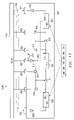
Pull up circuits 621–623 are located on the inputs of test buffers 609, 612, and 615. The purpose of the pull up circuits is to force the test circuitry into a state that will not interfere with the functional operation of the circuits A–I when the die is not being tested. For example, if test pads 601, 604, and 607 are not being driven by an external circuit/tester, the pull up circuits will force the inputs of test buffers 609, 612, and 615 high. Since test buffers 609, 612, and 615 are inverting types, their outputs will be set low while their inputs are high. In this example, a low on the outputs of test buffers 609, 612, and 615 will disable the outputs of test buffers 610, 611, 613, and 614, and enable the outputs of test isolation buffers 617 and 618. Thus circuits D, E, and F of FIG. 6 may functionally communicate via the test isolation buffers 617 and 618 while test pads 601, 604, and 607 are not being driven low by an external circuit/tester.
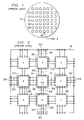
From the above description of FIGS. 6–8 and in reference to the die circuit example of FIG. 5 , it is clear that only circuit A receives test input exclusively from die pads 203 and only circuit I transmits test output exclusively from die pads 204. Thus circuit A test buffer 709 of FIG. 7 need only control (i.e. enable/disable) the outputs of test buffers and test isolation buffers associated with the output terminals 202 of circuit A, and circuit I test buffer 815 of FIG. 8 need only control the outputs of test buffers and test isolation buffers associated with the input terminals 201 of circuit I. The test enable buffers of circuits B, C, D, F, G, and H of die 501 will need to control the outputs of all test buffers and test isolation buffers that are associated with each circuit's input 201 and output 202 terminals. Circuit E of die 501 is the only circuit that receives test input and transmits test output exclusively using test pads 502. All other circuits in die 501 receive test input and transmit test output using a combination of die pads 203 and 204 and test pads 502.
As can be seen from FIG. 13 , when the die is placed in test mode by a low on test pad 1210, the outputs of test isolation buffers 1208 and 1209 are disabled and the outputs of test buffers 1211 and 1212 are enabled. In this mode the tester can simultaneously input different test data to circuits A and D via test pads 1203 and 1204 respectively, and output different test data from circuits C and F via test pads 1206 and 1207 respectively. Thus circuits A and D, and circuits C and F can be simultaneously tested by the application of test pads and associated test and isolation buffers at their shared input and output terminals.
When the test enable pad 1403 is driven high by an external circuit/tester, the outputs of the functional buffers 1503, 1505, 1507, 1508, and 1510 will be enabled to allow functional signals from circuits D and B to be input to functional circuitry 1530 of circuit E. When test enable pad 1403 is driven low by an external circuit/tester, the outputs of the test buffers 1502, 1504, 1506, 1509, and 1511 will be enabled to allow test data from an external circuit/test to be input to the functional circuitry 1530 via test pads 1402. When test enable pad 1403 is not externally driven, a pull up circuit 1522 will force the test enable input terminal 1406 high to force functional operation of circuit E 1501.
In comparing the functional output to input connections between circuits D and E of FIGS. 5 and 6 to the function output to input connections of circuits D and E of FIGS. 14 and 15 , it is seen that the functionality of the test isolation buffers 617 of FIG. 6 is provided by the function input buffers 1503, 1505, 1507, 1508, and 1510 of FIG. 15 . Thus circuits such as E 1501 that include input terminals for test 1405 and functional 201 inputs and multiplexing to select either the test or functional input to be input to functional circuitry 1530 provide a way to eliminate the need for external test isolation buffers 617 of FIG. 6 . As can be understood, this improves the signaling time between circuits D and E since the delay associated with the external test isolation buffers 617 of FIG. 6 is not present in the signaling paths between D and E of FIG. 15 .
It should be understood that the test enable pad 1403 of FIGS. 14 and 15 could also be connected to control the outputs of externally positioned test buffers and test isolation buffers, as test enable pad 1001 is shown doing in FIG. 10 . Also it should be understood that if all circuits A–I of FIG. 14 used test 1405 and functional 201 input terminals and internal multiplexing as shown in FIG. 15 , no externally positioned test isolation buffers 917 would be required in any of the output to input terminal connections 206 between circuits A–I or in the connections 205 between input pads 203 and input terminals 201 of circuits A, D, G, B, and C.
From the descriptions given in regard to FIGS. 5–15 , it is seen that the two problems mentioned in regard to FIGS. 3 and 4 have been solved. The first problem, regarding test wiring overhead, is solved since the top surface test pads 502 only require a small amount of local test wiring at each of the circuits A–I being tested. The second problem, regarding test time, is solved since the local top surface test pads allow simultaneous testing of each of the circuits A–I.
During simultaneous testing of multiple circuits A–I in a die, the power consumption may increase beyond the normal functional power consumption. The reason for this is that during normal functional operation of a die, only some of the circuits may be operating at any one time. However during test, a tester may operate all the circuits at the same time in order to quickly complete the testing of a die.
It should be understood that while the voltages of FIGS. 16 and 17 were mentioned as being power and ground, the die could be a mixed signal type requiring additional voltages to operate analog circuitry within the die. If other voltage supplies are required, these other voltages could be supplemented with test pads as described for the power and ground supplies of FIG. 17 .
It should be understood that while this disclosure has used buffers as the circuitry for coupling test pads (603, 605) to input and output terminals (201, 202) of circuits A–I, other types of switching circuitry could be used as well. For example, transmission gates could be used to couple circuit A–I input and output terminals to test pads.
It should be understood that while this disclosure has used buffers (617, 618) as the circuitry for isolating input and output terminals (201, 202) of circuits A–I during test, other types of switching circuitry could be used as well. For example, transmission gates could be used to isolate the input and output terminals of circuit A–I from each other during test.
It should also be understood that the circuits A–I could be digital, analog, or mixed signal circuit types, and said test inputs and/or test outputs to those circuit types could be in digital (1 and 0) or analog (continuously varying) signaling form.
It should be understood that when a die having test pads (502, 1503, 1506) processed on the top surface is prepared for packaging or assembly, an insulating layer may be processed on the top surface of the die to shield the test pads (power, ground, enable, input, and output test pads) from further external contact.
Although the present invention has been described in accordance to the embodiments shown in the figures, one of ordinary skill in the art will recognize there could be variations to these embodiments and those variations should be within the spirit and scope of the present invention. Accordingly, modifications may be made by one ordinarily skilled in the art without departing from the spirit and scope of the appended claims.
Claims (7)
1. A process of fabricating a die on a wafer of semiconductor material comprising:
A. producing the die to have a periphery, to have functional bond pads at the periphery, to have plural embedded core circuits, to have functional input terminals and functional output terminals for each embedded core circuit, and to have connections formed between certain ones of the functional input terminals and functional output terminals, to have connections formed between certain ones of the functional input terminals and functional bond pads, and to have connections formed between certain ones of the functional output terminals and functional bond pads; and
B. forming test enable circuits in the die coupled to the functional input terminals and functional output terminals between the embedded core circuits.
2. The process of claim 1 including forming on the wafer a test enable input pad separate from the functional pads and connected to the test enable circuits.
3. The process of claim 1 including forming on the wafer a test enable input pad that is spaced from the periphery, is separate from the functional pads and is connected to the test enable circuits.
4. The process of claim 1 in which the forming test enable circuits includes forming separately enabled test enable circuits for each embedded core circuit, and including forming on the wafer a test enable input pad for each embedded core circuit separate from the functional pads and connected to the test enable circuits for that embedded core circuit.
5. The process of claim 1 including forming on the die a test enable input pad separate from the functional pads and connected to the test enable circuits.
6. The process of claim 1 including forming on the die a test enable input pad that is spaced from the periphery, is separate from the functional pads and is connected to the test enable circuits.
7. The process of claim 1 in which the forming test enable circuits includes forming separately enabled test enable circuits for each embedded core circuit, and including forming on the die a test enable input pad for each embedded core circuit separate from the functional pads and connected to the test enable circuits for that embedded core circuit.
Priority Applications (13)
| Application Number | Priority Date | Filing Date | Title |
|---|---|---|---|
| US10/610,437 US7056752B2 (en) | 2001-01-19 | 2003-06-30 | Fabricating a die with test enable circuits between embedded cores |
| US11/279,509 US7368304B2 (en) | 2001-01-19 | 2006-04-12 | Fabricating die with separate test pads selectively coupled to cores |
| US12/047,907 US7569853B2 (en) | 2001-01-19 | 2008-03-13 | Test pads on leads unconnected with die pads |
| US12/495,060 US7956357B2 (en) | 2001-01-19 | 2009-06-30 | Test pads coupled with leads unconnected with die pads |
| US13/097,352 US8168970B2 (en) | 2001-01-19 | 2011-04-29 | Die having embedded circuitry with test and test enable circuitry |
| US13/432,667 US8466464B2 (en) | 2001-01-19 | 2012-03-28 | Test and enable circuitry connected between embedded die circuits |
| US13/894,051 US8742415B2 (en) | 2001-01-19 | 2013-05-14 | Test circuitry coupled to embedded circuit input/output unconnected to pads |
| US14/258,651 US8941109B2 (en) | 2001-01-19 | 2014-04-22 | Test output buffer functional output input, test output, enable input |
| US14/570,425 US9245812B2 (en) | 2001-01-19 | 2014-12-15 | Die with separate functional input, test out, enable input buffers |
| US14/946,061 US9472478B2 (en) | 2001-01-19 | 2015-11-19 | Die testing using top surface test pads |
| US15/267,996 US10690717B2 (en) | 2001-01-19 | 2016-09-16 | Enable input buffer coupling enable pad, functional circuitry, test circuit |
| US15/847,156 US10281522B2 (en) | 2001-01-19 | 2017-12-19 | Test circuitry coupling test pad to functional core input pad |
| US16/875,628 US10809295B2 (en) | 2001-01-19 | 2020-05-15 | Die testing using top surface test pads |
Applications Claiming Priority (3)
| Application Number | Priority Date | Filing Date | Title |
|---|---|---|---|
| US26313401P | 2001-01-19 | 2001-01-19 | |
| US10/051,536 US6590225B2 (en) | 2001-01-19 | 2002-01-18 | Die testing using top surface test pads |
| US10/610,437 US7056752B2 (en) | 2001-01-19 | 2003-06-30 | Fabricating a die with test enable circuits between embedded cores |
Related Parent Applications (1)
| Application Number | Title | Priority Date | Filing Date |
|---|---|---|---|
| US10/051,536 Division US6590225B2 (en) | 2001-01-19 | 2002-01-18 | Die testing using top surface test pads |
Related Child Applications (1)
| Application Number | Title | Priority Date | Filing Date |
|---|---|---|---|
| US11/279,509 Division US7368304B2 (en) | 2001-01-19 | 2006-04-12 | Fabricating die with separate test pads selectively coupled to cores |
Publications (2)
| Publication Number | Publication Date |
|---|---|
| US20040101985A1 US20040101985A1 (en) | 2004-05-27 |
| US7056752B2 true US7056752B2 (en) | 2006-06-06 |
Family
ID=26729529
Family Applications (14)
| Application Number | Title | Priority Date | Filing Date |
|---|---|---|---|
| US10/051,536 Expired - Lifetime US6590225B2 (en) | 2001-01-19 | 2002-01-18 | Die testing using top surface test pads |
| US10/610,437 Expired - Lifetime US7056752B2 (en) | 2001-01-19 | 2003-06-30 | Fabricating a die with test enable circuits between embedded cores |
| US11/279,509 Expired - Lifetime US7368304B2 (en) | 2001-01-19 | 2006-04-12 | Fabricating die with separate test pads selectively coupled to cores |
| US12/047,907 Expired - Fee Related US7569853B2 (en) | 2001-01-19 | 2008-03-13 | Test pads on leads unconnected with die pads |
| US12/495,060 Expired - Fee Related US7956357B2 (en) | 2001-01-19 | 2009-06-30 | Test pads coupled with leads unconnected with die pads |
| US13/097,352 Expired - Lifetime US8168970B2 (en) | 2001-01-19 | 2011-04-29 | Die having embedded circuitry with test and test enable circuitry |
| US13/432,667 Expired - Lifetime US8466464B2 (en) | 2001-01-19 | 2012-03-28 | Test and enable circuitry connected between embedded die circuits |
| US13/894,051 Expired - Fee Related US8742415B2 (en) | 2001-01-19 | 2013-05-14 | Test circuitry coupled to embedded circuit input/output unconnected to pads |
| US14/258,651 Expired - Fee Related US8941109B2 (en) | 2001-01-19 | 2014-04-22 | Test output buffer functional output input, test output, enable input |
| US14/570,425 Expired - Fee Related US9245812B2 (en) | 2001-01-19 | 2014-12-15 | Die with separate functional input, test out, enable input buffers |
| US14/946,061 Expired - Lifetime US9472478B2 (en) | 2001-01-19 | 2015-11-19 | Die testing using top surface test pads |
| US15/267,996 Expired - Lifetime US10690717B2 (en) | 2001-01-19 | 2016-09-16 | Enable input buffer coupling enable pad, functional circuitry, test circuit |
| US15/847,156 Expired - Lifetime US10281522B2 (en) | 2001-01-19 | 2017-12-19 | Test circuitry coupling test pad to functional core input pad |
| US16/875,628 Expired - Lifetime US10809295B2 (en) | 2001-01-19 | 2020-05-15 | Die testing using top surface test pads |
Family Applications Before (1)
| Application Number | Title | Priority Date | Filing Date |
|---|---|---|---|
| US10/051,536 Expired - Lifetime US6590225B2 (en) | 2001-01-19 | 2002-01-18 | Die testing using top surface test pads |
Family Applications After (12)
| Application Number | Title | Priority Date | Filing Date |
|---|---|---|---|
| US11/279,509 Expired - Lifetime US7368304B2 (en) | 2001-01-19 | 2006-04-12 | Fabricating die with separate test pads selectively coupled to cores |
| US12/047,907 Expired - Fee Related US7569853B2 (en) | 2001-01-19 | 2008-03-13 | Test pads on leads unconnected with die pads |
| US12/495,060 Expired - Fee Related US7956357B2 (en) | 2001-01-19 | 2009-06-30 | Test pads coupled with leads unconnected with die pads |
| US13/097,352 Expired - Lifetime US8168970B2 (en) | 2001-01-19 | 2011-04-29 | Die having embedded circuitry with test and test enable circuitry |
| US13/432,667 Expired - Lifetime US8466464B2 (en) | 2001-01-19 | 2012-03-28 | Test and enable circuitry connected between embedded die circuits |
| US13/894,051 Expired - Fee Related US8742415B2 (en) | 2001-01-19 | 2013-05-14 | Test circuitry coupled to embedded circuit input/output unconnected to pads |
| US14/258,651 Expired - Fee Related US8941109B2 (en) | 2001-01-19 | 2014-04-22 | Test output buffer functional output input, test output, enable input |
| US14/570,425 Expired - Fee Related US9245812B2 (en) | 2001-01-19 | 2014-12-15 | Die with separate functional input, test out, enable input buffers |
| US14/946,061 Expired - Lifetime US9472478B2 (en) | 2001-01-19 | 2015-11-19 | Die testing using top surface test pads |
| US15/267,996 Expired - Lifetime US10690717B2 (en) | 2001-01-19 | 2016-09-16 | Enable input buffer coupling enable pad, functional circuitry, test circuit |
| US15/847,156 Expired - Lifetime US10281522B2 (en) | 2001-01-19 | 2017-12-19 | Test circuitry coupling test pad to functional core input pad |
| US16/875,628 Expired - Lifetime US10809295B2 (en) | 2001-01-19 | 2020-05-15 | Die testing using top surface test pads |
Country Status (1)
| Country | Link |
|---|---|
| US (14) | US6590225B2 (en) |
Cited By (2)
| Publication number | Priority date | Publication date | Assignee | Title |
|---|---|---|---|---|
| US20090114912A1 (en) * | 2007-11-01 | 2009-05-07 | Texas Instruments Incorporated | Mask design elements to aid circuit editing and mask redesign |
| US20110204915A1 (en) * | 2001-01-19 | 2011-08-25 | Texas Instruments Incorporated | Die testing using top surface test pads |
Families Citing this family (23)
| Publication number | Priority date | Publication date | Assignee | Title |
|---|---|---|---|---|
| US7549987B2 (en) * | 2000-12-09 | 2009-06-23 | Tsunami Medtech, Llc | Thermotherapy device |
| US6809378B2 (en) * | 2001-08-30 | 2004-10-26 | Micron Technology, Inc. | Structure for temporarily isolating a die from a common conductor to facilitate wafer level testing |
| US7124341B2 (en) * | 2002-01-18 | 2006-10-17 | Texas Instruments Incorporated | Integrated circuit having electrically isolatable test circuitry |
| JP3895206B2 (en) * | 2002-03-29 | 2007-03-22 | 日本電波工業株式会社 | Oscillator sheet substrate and surface mount crystal oscillator manufacturing method using the same |
| US7026646B2 (en) * | 2002-06-20 | 2006-04-11 | Micron Technology, Inc. | Isolation circuit |
| US6967348B2 (en) * | 2002-06-20 | 2005-11-22 | Micron Technology, Inc. | Signal sharing circuit with microelectric die isolation features |
| JP4510370B2 (en) * | 2002-12-25 | 2010-07-21 | パナソニック株式会社 | Semiconductor integrated circuit device |
| GB0329516D0 (en) * | 2003-12-19 | 2004-01-28 | Univ Kent Canterbury | Integrated circuit with debug support interface |
| JP4592634B2 (en) * | 2005-06-17 | 2010-12-01 | パナソニック株式会社 | Semiconductor device |
| TWI264127B (en) * | 2005-09-23 | 2006-10-11 | Via Tech Inc | Chip package and substrate thereof |
| JP4745007B2 (en) * | 2005-09-29 | 2011-08-10 | 三洋電機株式会社 | Semiconductor device and manufacturing method thereof |
| CN1980549A (en) * | 2005-12-09 | 2007-06-13 | 深圳富泰宏精密工业有限公司 | Chip-card holding structure |
| US20070195682A1 (en) * | 2006-02-21 | 2007-08-23 | Duerig Urs T | Method for high density data storage and imaging |
| US7750660B2 (en) * | 2006-03-30 | 2010-07-06 | Qualcomm Incorporated | Integrated circuit with improved test capability via reduced pin count |
| KR20070099986A (en) * | 2006-04-06 | 2007-10-10 | 삼성전자주식회사 | Film type package and display apparatus having the same |
| JP2011149775A (en) * | 2010-01-20 | 2011-08-04 | Renesas Electronics Corp | Semiconductor integrated circuit and core test circuit |
| JP2011249366A (en) * | 2010-05-21 | 2011-12-08 | Panasonic Corp | Semiconductor device and manufacturing method thereof |
| DE102010046214A1 (en) | 2010-09-21 | 2012-03-22 | Infineon Technologies Ag | Wafer test structure has interface that is connected to integrated test circuit, for receiving and outputting test data |
| US8643189B1 (en) * | 2012-07-17 | 2014-02-04 | Freescale Semiconductor, Inc. | Packaged semiconductor die with power rail pads |
| KR101883386B1 (en) * | 2015-03-16 | 2018-07-30 | 주식회사 엘지화학 | Battery Compression Stopper And Battery Module Comprising The Same |
| JP6818512B2 (en) * | 2016-10-27 | 2021-01-20 | 株式会社ジャパンディスプレイ | Display device and manufacturing method of display device |
| US11047904B2 (en) | 2019-03-05 | 2021-06-29 | Nxp Usa, Inc. | Low power mode testing in an integrated circuit |
| KR20210113492A (en) * | 2020-03-06 | 2021-09-16 | 에스케이하이닉스 주식회사 | Semiconductor substrate, semiconductor package including the semi.conductor substrate and test method of the semiconductor substrate |
Citations (4)
| Publication number | Priority date | Publication date | Assignee | Title |
|---|---|---|---|---|
| US5506499A (en) * | 1995-06-05 | 1996-04-09 | Neomagic Corp. | Multiple probing of an auxilary test pad which allows for reliable bonding to a primary bonding pad |
| US6097098A (en) * | 1997-02-14 | 2000-08-01 | Micron Technology, Inc. | Die interconnections using intermediate connection elements secured to the die face |
| US6180426B1 (en) * | 1999-03-01 | 2001-01-30 | Mou-Shiung Lin | High performance sub-system design and assembly |
| US6535999B1 (en) * | 1999-07-13 | 2003-03-18 | Micron Technology, Inc. | Test and observe mode for embedded memory |
Family Cites Families (23)
| Publication number | Priority date | Publication date | Assignee | Title |
|---|---|---|---|---|
| US4488267A (en) * | 1982-05-24 | 1984-12-11 | At&T Bell Laboratories | Integrated circuit chips with removable drivers and/or buffers |
| KR880014482A (en) * | 1987-05-27 | 1988-12-24 | 미다 가쓰시게 | Semiconductor integrated circuit device |
| JP2827229B2 (en) * | 1988-10-14 | 1998-11-25 | 日本電気株式会社 | Semiconductor integrated circuit |
| US4956602A (en) * | 1989-02-14 | 1990-09-11 | Amber Engineering, Inc. | Wafer scale testing of redundant integrated circuit dies |
| US5053700A (en) * | 1989-02-14 | 1991-10-01 | Amber Engineering, Inc. | Method for wafer scale testing of redundant integrated circuit dies |
| JP2513904B2 (en) * | 1990-06-12 | 1996-07-10 | 株式会社東芝 | Testability circuit |
| EP0481703B1 (en) * | 1990-10-15 | 2003-09-17 | Aptix Corporation | Interconnect substrate having integrated circuit for programmable interconnection and sample testing |
| US5254940A (en) * | 1990-12-13 | 1993-10-19 | Lsi Logic Corporation | Testable embedded microprocessor and method of testing same |
| US5594273A (en) * | 1993-07-23 | 1997-01-14 | Motorola Inc. | Apparatus for performing wafer-level testing of integrated circuits where test pads lie within integrated circuit die but overly no active circuitry for improved yield |
| US5799021A (en) * | 1994-10-28 | 1998-08-25 | Duet Technologies, Inc. | Method for direct access test of embedded cells and customization logic |
| JPH08148537A (en) * | 1994-11-18 | 1996-06-07 | Toshiba Corp | Semiconductor integrated circuit |
| US6055659A (en) * | 1999-02-26 | 2000-04-25 | Texas Instruments Incorporated | Boundary scan with latching output buffer and weak input buffer |
| JPH09139471A (en) * | 1995-09-07 | 1997-05-27 | Hewlett Packard Co <Hp> | Auxiliary pad for on-circuit-array probing |
| US5969538A (en) * | 1996-10-31 | 1999-10-19 | Texas Instruments Incorporated | Semiconductor wafer with interconnect between dies for testing and a process of testing |
| US6046600A (en) * | 1995-10-31 | 2000-04-04 | Texas Instruments Incorporated | Process of testing integrated circuit dies on a wafer |
| US5994912A (en) * | 1995-10-31 | 1999-11-30 | Texas Instruments Incorporated | Fault tolerant selection of die on wafer |
| US5760643A (en) * | 1995-10-31 | 1998-06-02 | Texas Instruments Incorporated | Integrated circuit die with selective pad-to-pad bypass of internal circuitry |
| US7362093B2 (en) * | 1995-10-31 | 2008-04-22 | Texas Instruments Incorporated | IC selectively connecting logic and bypass conductors between opposing pads |
| US6326801B1 (en) * | 1996-10-31 | 2001-12-04 | Texas Instruments Incorporated | Wafer of semiconductor material with dies, probe areas and leads |
| US6199182B1 (en) * | 1997-03-27 | 2001-03-06 | Texas Instruments Incorporated | Probeless testing of pad buffers on wafer |
| US6169418B1 (en) * | 1998-06-24 | 2001-01-02 | S3 Incorporated | Efficient routing from multiple sources to embedded DRAM and other large circuit blocks |
| JP4234244B2 (en) * | 1998-12-28 | 2009-03-04 | 富士通マイクロエレクトロニクス株式会社 | Wafer level package and semiconductor device manufacturing method using wafer level package |
| US6590225B2 (en) * | 2001-01-19 | 2003-07-08 | Texas Instruments Incorporated | Die testing using top surface test pads |
-
2002
- 2002-01-18 US US10/051,536 patent/US6590225B2/en not_active Expired - Lifetime
-
2003
- 2003-06-30 US US10/610,437 patent/US7056752B2/en not_active Expired - Lifetime
-
2006
- 2006-04-12 US US11/279,509 patent/US7368304B2/en not_active Expired - Lifetime
-
2008
- 2008-03-13 US US12/047,907 patent/US7569853B2/en not_active Expired - Fee Related
-
2009
- 2009-06-30 US US12/495,060 patent/US7956357B2/en not_active Expired - Fee Related
-
2011
- 2011-04-29 US US13/097,352 patent/US8168970B2/en not_active Expired - Lifetime
-
2012
- 2012-03-28 US US13/432,667 patent/US8466464B2/en not_active Expired - Lifetime
-
2013
- 2013-05-14 US US13/894,051 patent/US8742415B2/en not_active Expired - Fee Related
-
2014
- 2014-04-22 US US14/258,651 patent/US8941109B2/en not_active Expired - Fee Related
- 2014-12-15 US US14/570,425 patent/US9245812B2/en not_active Expired - Fee Related
-
2015
- 2015-11-19 US US14/946,061 patent/US9472478B2/en not_active Expired - Lifetime
-
2016
- 2016-09-16 US US15/267,996 patent/US10690717B2/en not_active Expired - Lifetime
-
2017
- 2017-12-19 US US15/847,156 patent/US10281522B2/en not_active Expired - Lifetime
-
2020
- 2020-05-15 US US16/875,628 patent/US10809295B2/en not_active Expired - Lifetime
Patent Citations (4)
| Publication number | Priority date | Publication date | Assignee | Title |
|---|---|---|---|---|
| US5506499A (en) * | 1995-06-05 | 1996-04-09 | Neomagic Corp. | Multiple probing of an auxilary test pad which allows for reliable bonding to a primary bonding pad |
| US6097098A (en) * | 1997-02-14 | 2000-08-01 | Micron Technology, Inc. | Die interconnections using intermediate connection elements secured to the die face |
| US6180426B1 (en) * | 1999-03-01 | 2001-01-30 | Mou-Shiung Lin | High performance sub-system design and assembly |
| US6535999B1 (en) * | 1999-07-13 | 2003-03-18 | Micron Technology, Inc. | Test and observe mode for embedded memory |
Cited By (7)
| Publication number | Priority date | Publication date | Assignee | Title |
|---|---|---|---|---|
| US20110204915A1 (en) * | 2001-01-19 | 2011-08-25 | Texas Instruments Incorporated | Die testing using top surface test pads |
| US8168970B2 (en) * | 2001-01-19 | 2012-05-01 | Texas Instruments Incorporated | Die having embedded circuitry with test and test enable circuitry |
| US10281522B2 (en) | 2001-01-19 | 2019-05-07 | Texas Instruments Incorporated | Test circuitry coupling test pad to functional core input pad |
| US10690717B2 (en) | 2001-01-19 | 2020-06-23 | Texas Instruments Incorporated | Enable input buffer coupling enable pad, functional circuitry, test circuit |
| US10809295B2 (en) | 2001-01-19 | 2020-10-20 | Texas Instruments Incorporated | Die testing using top surface test pads |
| US20090114912A1 (en) * | 2007-11-01 | 2009-05-07 | Texas Instruments Incorporated | Mask design elements to aid circuit editing and mask redesign |
| US8330159B2 (en) | 2007-11-01 | 2012-12-11 | Texas Instruments Incorporated | Mask design elements to aid circuit editing and mask redesign |
Also Published As
| Publication number | Publication date |
|---|---|
| US7956357B2 (en) | 2011-06-07 |
| US20200278389A1 (en) | 2020-09-03 |
| US9245812B2 (en) | 2016-01-26 |
| US7368304B2 (en) | 2008-05-06 |
| US20060205099A1 (en) | 2006-09-14 |
| US20120182033A1 (en) | 2012-07-19 |
| US10690717B2 (en) | 2020-06-23 |
| US10809295B2 (en) | 2020-10-20 |
| US8742415B2 (en) | 2014-06-03 |
| US20040101985A1 (en) | 2004-05-27 |
| US20150097186A1 (en) | 2015-04-09 |
| US20110204915A1 (en) | 2011-08-25 |
| US8941109B2 (en) | 2015-01-27 |
| US7569853B2 (en) | 2009-08-04 |
| US20080157803A1 (en) | 2008-07-03 |
| US10281522B2 (en) | 2019-05-07 |
| US20090261326A1 (en) | 2009-10-22 |
| US20020119650A1 (en) | 2002-08-29 |
| US20140225112A1 (en) | 2014-08-14 |
| US6590225B2 (en) | 2003-07-08 |
| US20130248864A1 (en) | 2013-09-26 |
| US20160079132A1 (en) | 2016-03-17 |
| US20180106858A1 (en) | 2018-04-19 |
| US8168970B2 (en) | 2012-05-01 |
| US9472478B2 (en) | 2016-10-18 |
| US8466464B2 (en) | 2013-06-18 |
| US20170003341A1 (en) | 2017-01-05 |
Similar Documents
| Publication | Publication Date | Title |
|---|---|---|
| US10809295B2 (en) | Die testing using top surface test pads | |
| US7880491B2 (en) | Multilayer semiconductor device | |
| KR20080050637A (en) | Mixed analog and digital integrated circuits | |
| US5097205A (en) | Ic chip test circuit for high frequency integrated circuits | |
| CN100530647C (en) | Semiconductor integrated circuit device | |
| US6121785A (en) | Circuit and a method for configuring pad connections in an integrated device | |
| US20040188853A1 (en) | Semiconductor device | |
| US20020097615A1 (en) | Connection pad arrangements for electronic circuit comprising both functional logic and Flash-EEPROM | |
| JPS63199439A (en) | Semiconductor integrated circuit device | |
| JPH04336442A (en) | Semiconductor ic | |
| JPH05121501A (en) | Semiconductor integrated circuit | |
| JP2001168273A (en) | Semiconductor device and its manufacturing method | |
| JPH10325851A (en) | Ic mounting tester jig for control | |
| JPS61120437A (en) | Semiconductor device |
Legal Events
| Date | Code | Title | Description |
|---|---|---|---|
| STCF | Information on status: patent grant |
Free format text: PATENTED CASE |
|
| FPAY | Fee payment |
Year of fee payment: 4 |
|
| FPAY | Fee payment |
Year of fee payment: 8 |
|
| MAFP | Maintenance fee payment |
Free format text: PAYMENT OF MAINTENANCE FEE, 12TH YEAR, LARGE ENTITY (ORIGINAL EVENT CODE: M1553) Year of fee payment: 12 |