US7057242B2 - Transistor structures having access gates with narrowed central portions - Google Patents
Transistor structures having access gates with narrowed central portions Download PDFInfo
- Publication number
- US7057242B2 US7057242B2 US10/264,136 US26413602A US7057242B2 US 7057242 B2 US7057242 B2 US 7057242B2 US 26413602 A US26413602 A US 26413602A US 7057242 B2 US7057242 B2 US 7057242B2
- Authority
- US
- United States
- Prior art keywords
- active region
- gate
- along
- access
- gate portion
- Prior art date
- Legal status (The legal status is an assumption and is not a legal conclusion. Google has not performed a legal analysis and makes no representation as to the accuracy of the status listed.)
- Expired - Lifetime
Links
- 239000000758 substrate Substances 0.000 claims abstract description 11
- 230000002093 peripheral effect Effects 0.000 description 6
- 229910052796 boron Inorganic materials 0.000 description 5
- 230000005684 electric field Effects 0.000 description 5
- ZOXJGFHDIHLPTG-UHFFFAOYSA-N Boron Chemical compound [B] ZOXJGFHDIHLPTG-UHFFFAOYSA-N 0.000 description 3
- 238000005204 segregation Methods 0.000 description 3
- -1 boron ions Chemical class 0.000 description 2
- 230000007423 decrease Effects 0.000 description 2
- 230000000694 effects Effects 0.000 description 2
- 238000000034 method Methods 0.000 description 2
- 238000000206 photolithography Methods 0.000 description 2
- XUIMIQQOPSSXEZ-UHFFFAOYSA-N Silicon Chemical compound [Si] XUIMIQQOPSSXEZ-UHFFFAOYSA-N 0.000 description 1
- 238000002955 isolation Methods 0.000 description 1
- 230000003647 oxidation Effects 0.000 description 1
- 238000007254 oxidation reaction Methods 0.000 description 1
- 229910052710 silicon Inorganic materials 0.000 description 1
- 239000010703 silicon Substances 0.000 description 1
Images


Classifications
-
- H—ELECTRICITY
- H01—ELECTRIC ELEMENTS
- H01L—SEMICONDUCTOR DEVICES NOT COVERED BY CLASS H10
- H01L21/00—Processes or apparatus adapted for the manufacture or treatment of semiconductor or solid state devices or of parts thereof
- H01L21/02—Manufacture or treatment of semiconductor devices or of parts thereof
- H01L21/04—Manufacture or treatment of semiconductor devices or of parts thereof the devices having at least one potential-jump barrier or surface barrier, e.g. PN junction, depletion layer or carrier concentration layer
- H01L21/18—Manufacture or treatment of semiconductor devices or of parts thereof the devices having at least one potential-jump barrier or surface barrier, e.g. PN junction, depletion layer or carrier concentration layer the devices having semiconductor bodies comprising elements of Group IV of the Periodic System or AIIIBV compounds with or without impurities, e.g. doping materials
- H01L21/28—Manufacture of electrodes on semiconductor bodies using processes or apparatus not provided for in groups H01L21/20 - H01L21/268
- H01L21/28008—Making conductor-insulator-semiconductor electrodes
- H01L21/28017—Making conductor-insulator-semiconductor electrodes the insulator being formed after the semiconductor body, the semiconductor being silicon
- H01L21/28026—Making conductor-insulator-semiconductor electrodes the insulator being formed after the semiconductor body, the semiconductor being silicon characterised by the conductor
- H01L21/28123—Lithography-related aspects, e.g. sub-lithography lengths; Isolation-related aspects, e.g. to solve problems arising at the crossing with the side of the device isolation; Planarisation aspects
-
- H—ELECTRICITY
- H10—SEMICONDUCTOR DEVICES; ELECTRIC SOLID-STATE DEVICES NOT OTHERWISE PROVIDED FOR
- H10B—ELECTRONIC MEMORY DEVICES
- H10B12/00—Dynamic random access memory [DRAM] devices
-
- H—ELECTRICITY
- H01—ELECTRIC ELEMENTS
- H01L—SEMICONDUCTOR DEVICES NOT COVERED BY CLASS H10
- H01L29/00—Semiconductor devices adapted for rectifying, amplifying, oscillating or switching, or capacitors or resistors with at least one potential-jump barrier or surface barrier, e.g. PN junction depletion layer or carrier concentration layer; Details of semiconductor bodies or of electrodes thereof ; Multistep manufacturing processes therefor
- H01L29/02—Semiconductor bodies ; Multistep manufacturing processes therefor
- H01L29/06—Semiconductor bodies ; Multistep manufacturing processes therefor characterised by their shape; characterised by the shapes, relative sizes, or dispositions of the semiconductor regions ; characterised by the concentration or distribution of impurities within semiconductor regions
- H01L29/10—Semiconductor bodies ; Multistep manufacturing processes therefor characterised by their shape; characterised by the shapes, relative sizes, or dispositions of the semiconductor regions ; characterised by the concentration or distribution of impurities within semiconductor regions with semiconductor regions connected to an electrode not carrying current to be rectified, amplified or switched and such electrode being part of a semiconductor device which comprises three or more electrodes
- H01L29/1025—Channel region of field-effect devices
- H01L29/1029—Channel region of field-effect devices of field-effect transistors
- H01L29/1033—Channel region of field-effect devices of field-effect transistors with insulated gate, e.g. characterised by the length, the width, the geometric contour or the doping structure
-
- H—ELECTRICITY
- H01—ELECTRIC ELEMENTS
- H01L—SEMICONDUCTOR DEVICES NOT COVERED BY CLASS H10
- H01L29/00—Semiconductor devices adapted for rectifying, amplifying, oscillating or switching, or capacitors or resistors with at least one potential-jump barrier or surface barrier, e.g. PN junction depletion layer or carrier concentration layer; Details of semiconductor bodies or of electrodes thereof ; Multistep manufacturing processes therefor
- H01L29/40—Electrodes ; Multistep manufacturing processes therefor
- H01L29/41—Electrodes ; Multistep manufacturing processes therefor characterised by their shape, relative sizes or dispositions
- H01L29/423—Electrodes ; Multistep manufacturing processes therefor characterised by their shape, relative sizes or dispositions not carrying the current to be rectified, amplified or switched
- H01L29/42312—Gate electrodes for field effect devices
- H01L29/42316—Gate electrodes for field effect devices for field-effect transistors
- H01L29/4232—Gate electrodes for field effect devices for field-effect transistors with insulated gate
- H01L29/42372—Gate electrodes for field effect devices for field-effect transistors with insulated gate characterised by the conducting layer, e.g. the length, the sectional shape or the lay-out
- H01L29/4238—Gate electrodes for field effect devices for field-effect transistors with insulated gate characterised by the conducting layer, e.g. the length, the sectional shape or the lay-out characterised by the surface lay-out
-
- H—ELECTRICITY
- H10—SEMICONDUCTOR DEVICES; ELECTRIC SOLID-STATE DEVICES NOT OTHERWISE PROVIDED FOR
- H10B—ELECTRONIC MEMORY DEVICES
- H10B12/00—Dynamic random access memory [DRAM] devices
- H10B12/01—Manufacture or treatment
- H10B12/02—Manufacture or treatment for one transistor one-capacitor [1T-1C] memory cells
- H10B12/05—Making the transistor
-
- H—ELECTRICITY
- H01—ELECTRIC ELEMENTS
- H01L—SEMICONDUCTOR DEVICES NOT COVERED BY CLASS H10
- H01L27/00—Devices consisting of a plurality of semiconductor or other solid-state components formed in or on a common substrate
- H01L27/02—Devices consisting of a plurality of semiconductor or other solid-state components formed in or on a common substrate including semiconductor components specially adapted for rectifying, oscillating, amplifying or switching and having at least one potential-jump barrier or surface barrier; including integrated passive circuit elements with at least one potential-jump barrier or surface barrier
- H01L27/0203—Particular design considerations for integrated circuits
- H01L27/0207—Geometrical layout of the components, e.g. computer aided design; custom LSI, semi-custom LSI, standard cell technique
Definitions
- the present invention relates to integrated circuit devices, and more particularly, to transistor structures for integrated circuit devices.
- shallow trench isolation As integrated circuits have been highly integrated, shallow trench isolation (STI) has replaced local oxidation of silicon (LOCOS) for isolating active regions, e.g., source and drain regions for transistors.
- LOCOS local oxidation of silicon
- the reduced area used for transistors can result in reduction of the threshold voltage Vth of the transistor.
- Such a phenomenon is called the “inverse narrow width effect,” which is illustrated in FIG. 1 .
- FIG. 2 is a view of the layout of a gate pattern 7 formed across an active region 3 and FIG. 3 is a cross-sectional view of the gate pattern 7 of FIG. 1 , taken along the lines III-III′.
- a gate oxide layer 4 is regrown after STI regions 2 are formed in a substrate 1 to define an active region 3
- boron ions 5 which have been doped on the substrate 1 to form a channel, are typically transferred to a gate oxide layer 4 .
- the density of the boron ions 5 at edge regions E of the active region 3 may decrease, thereby lowering a threshold voltage of a transistor. This phenomenon is referred to as boron segregation.
- portions 7 a of gate lines referred to as “access gates” are disposed on an active region 3 and have a length E that is sufficient to operate the transistors.
- Other gate line portions 7 b referred to as “pass gates” are formed on STI regions, and have a gate length L′ sufficient to propagate signals.
- limitations of the photolithography process used to fabricate the device may cause the gate length at a region E to be significantly shorter than the gate length at a region C, as indicated by dashed lines in FIG. 5 .
- the threshold voltage of a transistor at the region E can be reduced as much as to 60% in comparison to the threshold voltage at the region C. This can result in undesirably large sub-threshold leakage currents, and can deteriorate the dynamic refresh characteristics of the DRAM.
- an integrated circuit transistor includes an active region in a substrate, the active region elongated along a first direction.
- a gate pattern is disposed on the active region and extends across the active region along a second direction transverse to the first direction.
- the gate pattern has an extent along the first direction that is greater at a peripheral portion of the active region than at a center portion of the active region.
- the gate pattern linearly increases in extent along the first direction from the center portion of the active region towards the peripheral portion of the active region.
- the gate pattern exhibits a stepwise increase in extent along the first direction between the center portion of the active region and the peripheral portion of the active region.
- the gate pattern may increase in extent along the first direction from the center portion of the active region to a point beyond an edge of the active region at which the extent of the gate pattern along the first direction decreases.
- an integrated circuit transistor includes an active region in a substrate, elongated along a first direction.
- a gate pattern is disposed on the substrate and crosses the active region along a second direction transverse to the first direction.
- the gate pattern includes an access gate portion disposed on the active region and narrowed at a central portion thereof.
- the gate pattern may further include a pass gate portion adjoining the access gate portion at the point beyond the edge of the active region, the pass gate portion having a lesser extent along the first direction than the access gate portion.
- a transistor structure e.g., a transistor pair, includes an active region in a substrate, the active region having first and second protrusions extending in opposite directions along a first axis.
- First and second gate patterns are disposed on the active region, crossing respective ones of the first and second protrusions along a second direction transverse to the first direction.
- the first and second gate patterns increase in extent along the first direction from center portions of the first and second protrusions towards peripheral portions of the first and second protrusions.
- FIG. 1 is a graph showing relationships between transistor gate width and threshold voltage.
- FIG. 2 is a plan view of the layout of a conventional cell transistor.
- FIG. 3 is a cross-sectional view of the transistor of FIG. 2 .
- FIG. 4 is a graph showing relationships between gate length and threshold voltage.
- FIG. 5 is a view of the layout of another conventional cell transistor
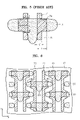
- FIG. 6 is a plan view of cell transistors according to some embodiments of the present invention.
- FIG. 7 is an enlarged view of a portion of FIG. 6 .
- FIG. 8 is a graph showing I–V characteristics of a cell transistor according to some embodiments of the present invention in comparison to characteristics of a conventional cell transistor.
- FIG. 9 is a graph showing sub-threshold swing characteristics of a cell transistor according embodiments of the present invention in comparison to characteristics of a conventional cell transistor.
- FIG. 10 is a plan view of cell transistors according to further embodiments of the present invention.
- FIG. 6 illustrates a cell transistor layout according to some embodiments of the present invention.
- Reference numerals 30 and 70 denote active regions and gate patterns, respectively.
- the active regions 30 are defined by STI regions, and are arrayed in a substrate 10 .
- the active region patterns 30 are elongated in an x direction, with first and second protrusions 30 a, 30 b that extend in opposite directions along the x direction.
- Third protrusions 30 c extend along the y direction, and are configured to be connected to bit lines (not shown).
- the gate patterns 70 extend along a y direction, transverse to the x direction. Two gate patterns 70 cross each active region 30 in a substantially orthogonal fashion, such that each active region 30 can form two memory cells.
- a gate pattern 70 includes an access gate (A.G.) portion 70 a pass gate (P.G.) portions 70 b.
- the access gate portion 70 a is disposed on the active region 30 .
- the pass gate portion 70 b is, disposed on the STI region and has a smaller critical dimension (CD) than the access gate portion 70 a.
- the access gate portion 70 a increases in extent along the x direction (or “length”) from a center portion C of the active region 30 toward peripheral portions E of the active region 30 .
- the relationship between the length L of the access gate portion 70 a at the center portion C of the active region 30 and the length L′ of the access gate portion 70 a at the peripheral portion E of the active region 30 is as follows: 1 ⁇ L′/L ⁇ 1.2 (1)
- the length of the access gate 70 a near the edges of the active region 30 may be the same or longer than the length of the access gate 70 a near the center portion C of the active region 30 .
- the access gate portion 70 a extends along the y direction such that a portion of the access gate portion 70 a extends onto the STI region.
- the extent along the y direction (or “width”) Wm of the extended portion is less than 25% of the width W of the active region 30 .
- the width W is less than about 200 nm, it is preferable that the extent Wm of the extended portion is less than about 50 nm.
- FIG. 8 is a graph showing I–V characteristics of a cell transistor according to some embodiments of the present invention.
- curve a represents a relationship between the gate to source voltage (Vgs) and drain current (Id) of a cell transistor according to embodiments of the invention having an access gate portion that is 0.33 ⁇ m long at its center.
- Curve b represents a relationship between the Vgs and Id of a conventional cell transistor that has an access gate whose center is 0.33 ⁇ m long, but is fabricated with the conventional configuration shown in FIG. 5 . From FIG.
- a threshold voltage Vth of the cell transistor according to embodiments of the present invention is comparable to that of the conventional cell transistor, sub-threshold leakage currents of the cell transistor according to the present invention can be reduced by an amount ⁇ LKG in comparison to the conventional cell transistor.
- FIG. 9 is a graph showing sub-threshold swing characteristics of cell transistors according to embodiments of the present invention in comparison to conventional cell transistors.
- Cell transistors according to the present invention have been fabricated with the configuration illustrated in FIGS. 6 and 7 with access gates whose centers are 0.29, 0.33 and 0.37 ⁇ m long, respectively.
- the symbols - ⁇ - and - ⁇ - denote swing values of some cell transistors according to some embodiments of the present invention, and - ⁇ - and -x- denote swing values of conventional cell transistors with comparable access gate lengths.
- the graph of FIG. 9 reveals that the swing values of transistors according to the present invention can be much smaller than those of conventional transistors of comparable access gate center length. Generally speaking, the shorter the access gate center length of the transistor, the smaller the swing value of the transistor.
- FIG. 10 is a view of the cell transistor layout according to further embodiments of the present invention.
- Tabs 70 ′T are formed near positions at which access gate portions 70 ′ a of gate patterns 70 ′ cross edge portions E of an active region 30 .
- the length of the access gate portions 70 ′ a at these positions E is greater than near the center portion C of the active region 30 , and increases in a stepwise fashion at the tabs 70 ′T.
- the tabs 70 ′T may be sized based on margins required during photolithography processes used to fabricate the device.
- the extent d of the tab patterns 70 ′T along the x direction is less than about 20% of the length C of the access gate at the center portion of the active region 30
- the extent c along the y direction is less than about 25% of the width W of the active region 30 .
- the extent d of the tab pattern 70 ′T is preferably less than 100 nm
- the extent c of the tab pattern 70 ′T is preferably less than 50 nm.
Abstract
Description
1<L′/L≦1.2 (1)
In an actual device, if the relationship between the lengths L and L′ is as shown in equation (1), the length of the
S=ΔVg/Δlog Id (2)
The graph of
Claims (3)
Applications Claiming Priority (2)
| Application Number | Priority Date | Filing Date | Title |
|---|---|---|---|
| KR2001-78284 | 2001-12-11 | ||
| KR10-2001-0078284A KR100464405B1 (en) | 2001-12-11 | 2001-12-11 | DRAM including a cell having a small value of subthreshold leakage currents |
Publications (2)
| Publication Number | Publication Date |
|---|---|
| US20030107094A1 US20030107094A1 (en) | 2003-06-12 |
| US7057242B2 true US7057242B2 (en) | 2006-06-06 |
Family
ID=19716900
Family Applications (1)
| Application Number | Title | Priority Date | Filing Date |
|---|---|---|---|
| US10/264,136 Expired - Lifetime US7057242B2 (en) | 2001-12-11 | 2002-10-03 | Transistor structures having access gates with narrowed central portions |
Country Status (2)
| Country | Link |
|---|---|
| US (1) | US7057242B2 (en) |
| KR (1) | KR100464405B1 (en) |
Cited By (1)
| Publication number | Priority date | Publication date | Assignee | Title |
|---|---|---|---|---|
| US20090261422A1 (en) * | 2007-09-18 | 2009-10-22 | Samsung Electronics Co., Ltd. | Cell structure of semiconductor device |
Families Citing this family (2)
| Publication number | Priority date | Publication date | Assignee | Title |
|---|---|---|---|---|
| KR101865840B1 (en) * | 2011-08-10 | 2018-06-08 | 삼성전자주식회사 | Semiconductor device |
| CN107706233B (en) * | 2016-08-08 | 2022-07-12 | 联华电子股份有限公司 | Semiconductor element and manufacturing method thereof |
Citations (7)
| Publication number | Priority date | Publication date | Assignee | Title |
|---|---|---|---|---|
| US5732009A (en) * | 1995-07-25 | 1998-03-24 | Hitachi, Ltd. | Semiconductor integrated circuit device including a DRAM in which a cell selection transistor has a stabilized threshold voltage |
| US5982008A (en) * | 1996-08-23 | 1999-11-09 | Kabushiki Kaisha Toshiba | Semiconductor device using a shallow trench isolation |
| US6168904B1 (en) * | 1997-09-29 | 2001-01-02 | Lucent Technologies Inc. | Integrated circuit fabrication |
| US6246080B1 (en) * | 1998-05-14 | 2001-06-12 | Nec Corporation | Semiconductor device having bent gate electrode and process for production thereof |
| US6346427B1 (en) * | 1999-08-18 | 2002-02-12 | Utmc Microelectronic Systems Inc. | Parameter adjustment in a MOS integrated circuit |
| US6424010B2 (en) * | 1996-11-15 | 2002-07-23 | Mitsubishi Denki Kabushiki Kaisha | Method of manufacturing a semiconductor device having reduced power consumption without a reduction in the source/drain breakdown voltage |
| US6462389B2 (en) * | 2000-01-27 | 2002-10-08 | Hyundai Electronics Industries Co., Ltd. | Semiconductor device |
Family Cites Families (3)
| Publication number | Priority date | Publication date | Assignee | Title |
|---|---|---|---|---|
| KR950011636B1 (en) * | 1992-03-04 | 1995-10-07 | 금성일렉트론주식회사 | Dynamic random access memory having reelected layout and layout design thereof |
| KR970000965B1 (en) * | 1993-01-30 | 1997-01-21 | 삼성전자 주식회사 | Gate electrode pattern layout of semiconductor device |
| JPH09321245A (en) * | 1996-05-30 | 1997-12-12 | Hitachi Ltd | Semiconductor integrated circuit device and manufacture thereof |
-
2001
- 2001-12-11 KR KR10-2001-0078284A patent/KR100464405B1/en active IP Right Grant
-
2002
- 2002-10-03 US US10/264,136 patent/US7057242B2/en not_active Expired - Lifetime
Patent Citations (7)
| Publication number | Priority date | Publication date | Assignee | Title |
|---|---|---|---|---|
| US5732009A (en) * | 1995-07-25 | 1998-03-24 | Hitachi, Ltd. | Semiconductor integrated circuit device including a DRAM in which a cell selection transistor has a stabilized threshold voltage |
| US5982008A (en) * | 1996-08-23 | 1999-11-09 | Kabushiki Kaisha Toshiba | Semiconductor device using a shallow trench isolation |
| US6424010B2 (en) * | 1996-11-15 | 2002-07-23 | Mitsubishi Denki Kabushiki Kaisha | Method of manufacturing a semiconductor device having reduced power consumption without a reduction in the source/drain breakdown voltage |
| US6168904B1 (en) * | 1997-09-29 | 2001-01-02 | Lucent Technologies Inc. | Integrated circuit fabrication |
| US6246080B1 (en) * | 1998-05-14 | 2001-06-12 | Nec Corporation | Semiconductor device having bent gate electrode and process for production thereof |
| US6346427B1 (en) * | 1999-08-18 | 2002-02-12 | Utmc Microelectronic Systems Inc. | Parameter adjustment in a MOS integrated circuit |
| US6462389B2 (en) * | 2000-01-27 | 2002-10-08 | Hyundai Electronics Industries Co., Ltd. | Semiconductor device |
Cited By (2)
| Publication number | Priority date | Publication date | Assignee | Title |
|---|---|---|---|---|
| US20090261422A1 (en) * | 2007-09-18 | 2009-10-22 | Samsung Electronics Co., Ltd. | Cell structure of semiconductor device |
| US8030697B2 (en) * | 2007-09-18 | 2011-10-04 | Samsung Electronics Co., Ltd. | Cell structure of semiconductor device having an active region with a concave portion |
Also Published As
| Publication number | Publication date |
|---|---|
| KR100464405B1 (en) | 2005-01-03 |
| KR20030047576A (en) | 2003-06-18 |
| US20030107094A1 (en) | 2003-06-12 |
Similar Documents
| Publication | Publication Date | Title |
|---|---|---|
| US5317178A (en) | Offset dual gate thin film field effect transistor | |
| US7932153B2 (en) | Semiconductor device and method for fabricating the same | |
| US6228704B1 (en) | Process for manufacturing semiconductor integrated circuit device | |
| KR20030029149A (en) | Trench-gate semiconductor device and its manufacturing method | |
| JP2007335887A (en) | Semiconductor device and its manufacturing method | |
| US7193275B2 (en) | Semiconductor device allowing modulation of a gain coefficient and a logic circuit provided with the same | |
| US20070278613A1 (en) | Semiconductor device | |
| US6136657A (en) | Method for fabricating a semiconductor device having different gate oxide layers | |
| US20070152262A1 (en) | Non-volatile memory device | |
| US7057242B2 (en) | Transistor structures having access gates with narrowed central portions | |
| US5936286A (en) | Differential poly-edge oxidation for stable SRAM cells | |
| KR100906643B1 (en) | Layout of wave type recess gate and method for fabricating recess gate using the same | |
| KR20010054136A (en) | Full CMOS SRAM cell | |
| EP0550177B1 (en) | Static RAM memory integrated circuit with balanced resistance | |
| US5241495A (en) | Semiconductor memory | |
| US7064453B2 (en) | Semiconductor memory device including a gate electrode with a recess | |
| US5438540A (en) | Semiconductor SRAM memory device | |
| US7009263B2 (en) | Field-effect transistor | |
| KR20090044481A (en) | Semiconductor device | |
| US5821564A (en) | TFT with self-align offset gate | |
| KR100282989B1 (en) | Semiconductor integrated circuit | |
| JPH04215473A (en) | Static ram | |
| KR20070036214A (en) | Sense amplifier in semiconductor device | |
| JPH0653442A (en) | Sram memory cell structure | |
| US7279749B2 (en) | Semiconductor device and semiconductor memory using the same |
Legal Events
| Date | Code | Title | Description |
|---|---|---|---|
| AS | Assignment |
Owner name: SAMSUNG ELECTRONICS CO., LTD., KOREA, REPUBLIC OF Free format text: ASSIGNMENT OF ASSIGNORS INTEREST;ASSIGNORS:KIM, JI-YOUNG;KIM, HYOUNG-SUB;REEL/FRAME:013364/0591 Effective date: 20020903 |
|
| STCF | Information on status: patent grant |
Free format text: PATENTED CASE |
|
| FEPP | Fee payment procedure |
Free format text: PAYOR NUMBER ASSIGNED (ORIGINAL EVENT CODE: ASPN); ENTITY STATUS OF PATENT OWNER: LARGE ENTITY |
|
| FEPP | Fee payment procedure |
Free format text: PAYER NUMBER DE-ASSIGNED (ORIGINAL EVENT CODE: RMPN); ENTITY STATUS OF PATENT OWNER: LARGE ENTITY Free format text: PAYOR NUMBER ASSIGNED (ORIGINAL EVENT CODE: ASPN); ENTITY STATUS OF PATENT OWNER: LARGE ENTITY |
|
| FPAY | Fee payment |
Year of fee payment: 4 |
|
| FPAY | Fee payment |
Year of fee payment: 8 |
|
| MAFP | Maintenance fee payment |
Free format text: PAYMENT OF MAINTENANCE FEE, 12TH YEAR, LARGE ENTITY (ORIGINAL EVENT CODE: M1553) Year of fee payment: 12 |