US7079216B2 - Manufacturing method of display device in which the main surface of the workpiece is at an angle - Google Patents
Manufacturing method of display device in which the main surface of the workpiece is at an angle Download PDFInfo
- Publication number
- US7079216B2 US7079216B2 US10/833,160 US83316004A US7079216B2 US 7079216 B2 US7079216 B2 US 7079216B2 US 83316004 A US83316004 A US 83316004A US 7079216 B2 US7079216 B2 US 7079216B2
- Authority
- US
- United States
- Prior art keywords
- substrate
- substrates
- mother substrates
- display device
- stacked mother
- Prior art date
- Legal status (The legal status is an assumption and is not a legal conclusion. Google has not performed a legal analysis and makes no representation as to the accuracy of the status listed.)
- Expired - Fee Related, expires
Links
Images


Classifications
-
- G—PHYSICS
- G02—OPTICS
- G02F—OPTICAL DEVICES OR ARRANGEMENTS FOR THE CONTROL OF LIGHT BY MODIFICATION OF THE OPTICAL PROPERTIES OF THE MEDIA OF THE ELEMENTS INVOLVED THEREIN; NON-LINEAR OPTICS; FREQUENCY-CHANGING OF LIGHT; OPTICAL LOGIC ELEMENTS; OPTICAL ANALOGUE/DIGITAL CONVERTERS
- G02F1/00—Devices or arrangements for the control of the intensity, colour, phase, polarisation or direction of light arriving from an independent light source, e.g. switching, gating or modulating; Non-linear optics
- G02F1/01—Devices or arrangements for the control of the intensity, colour, phase, polarisation or direction of light arriving from an independent light source, e.g. switching, gating or modulating; Non-linear optics for the control of the intensity, phase, polarisation or colour
- G02F1/13—Devices or arrangements for the control of the intensity, colour, phase, polarisation or direction of light arriving from an independent light source, e.g. switching, gating or modulating; Non-linear optics for the control of the intensity, phase, polarisation or colour based on liquid crystals, e.g. single liquid crystal display cells
- G02F1/133—Constructional arrangements; Operation of liquid crystal cells; Circuit arrangements
- G02F1/1333—Constructional arrangements; Manufacturing methods
- G02F1/133351—Manufacturing of individual cells out of a plurality of cells, e.g. by dicing
-
- C—CHEMISTRY; METALLURGY
- C03—GLASS; MINERAL OR SLAG WOOL
- C03B—MANUFACTURE, SHAPING, OR SUPPLEMENTARY PROCESSES
- C03B33/00—Severing cooled glass
- C03B33/02—Cutting or splitting sheet glass or ribbons; Apparatus or machines therefor
- C03B33/023—Cutting or splitting sheet glass or ribbons; Apparatus or machines therefor the sheet or ribbon being in a horizontal position
- C03B33/033—Apparatus for opening score lines in glass sheets
-
- C—CHEMISTRY; METALLURGY
- C03—GLASS; MINERAL OR SLAG WOOL
- C03B—MANUFACTURE, SHAPING, OR SUPPLEMENTARY PROCESSES
- C03B33/00—Severing cooled glass
- C03B33/07—Cutting armoured, multi-layered, coated or laminated, glass products
-
- C—CHEMISTRY; METALLURGY
- C03—GLASS; MINERAL OR SLAG WOOL
- C03B—MANUFACTURE, SHAPING, OR SUPPLEMENTARY PROCESSES
- C03B33/00—Severing cooled glass
- C03B33/10—Glass-cutting tools, e.g. scoring tools
-
- B—PERFORMING OPERATIONS; TRANSPORTING
- B65—CONVEYING; PACKING; STORING; HANDLING THIN OR FILAMENTARY MATERIAL
- B65G—TRANSPORT OR STORAGE DEVICES, e.g. CONVEYORS FOR LOADING OR TIPPING, SHOP CONVEYOR SYSTEMS OR PNEUMATIC TUBE CONVEYORS
- B65G2249/00—Aspects relating to conveying systems for the manufacture of fragile sheets
- B65G2249/04—Arrangements of vacuum systems or suction cups
Definitions
- the present invention relates to a method of manufacture and a device for the manufacture of a display device in which individual display device substrate-units are separated from stacked mother substrates.
- a planar panel type display device is constituted such that two sheets of large-sized substrates (referred to as stacked mother substrates hereinafter), formed of a first substrate (in general, a glass substrate, simply referred to as a substrate) and a second substrate which are laminated to each other while incorporating pixel regions of a plurality of unit display devices, are separated into individual display device substrate-units, and drive circuits are incorporated into terminals pulled out from the pixel regions.
- scribe lines are formed on the first substrate, and, after turning the stacked mother substrates up side down, the stacked mother substrates are broken along the scribe lines.
- scribe lines are formed on the second substrate and the stacked mother substrates are again turned up side down and are broken along the scribe lines. Thereafter, peripheral portions for exposing terminal portions are removed as wastage.
- a so-called scribing and breaking method is adopted.
- the stacked mother substrates PN on which the scribe lines are formed are mounted on a break table which has a metal plate, such as a stainless-steel plate, mounted on a cushion sheet made of rubber, sponge or the like in a state such that the scribe lines along which the substrates are to be broken are set at the break table side, and, thereafter, the stacked mother substrates are broken by being hit by a breaking bar made of a rubber member or the like from a side opposite to the scribe lines along the scribe lines or by having a pushing force applied thereto.
- JP-A-6-3633 discloses a scribing and breaking method in which respective stacked glass substrates are clamped using a pair of clamps while sandwiching the scribe line and the stacked glass substrates are broken by rotating one clamp at the scribe line.
- FIG. 19 is a diagram showing a working example of the use of scribing lines in a conventional scribing and breaking method.
- 9 display device substrate-units are obtained from the stacked mother substrates formed of two substrates SUB 1 and SUB 2 is shown.
- the first substrate SUB 1 front surface of stacked mother substrates in FIG. 22
- eight scribe lines SBL 1 in total consisting of four scribe lines in the X direction and four scribe lines in the Y direction are formed.
- scribe lines SBL 2 which are formed on the surface of the second substrate SUB 2 (back surface of the stacked mother substrates)
- eight scribe lines SBL 2 which are formed at the same positions as the scribe lines SBL 1 formed on the first substrate SUB 1
- four additional scribe lines SBL 2 are formed. Accordingly, twenty scribe lines in total become necessary at front and back surfaces of the stacked mother substrates.
- the scribe lines are formed at the same positions on the front and back surfaces of the first and second substrates and portions which are separated along the scribe lines become the wastage. Further, with respect to the scribe lines which are formed inside the stacked mother substrates, there exist scribe lines which are formed at the same positions at the front and back surfaces and scribe lines SBL 2 which are formed at different positions from the scribe lines SBL 1 only with respect to the second substrate SUB 2 .
- the substrate between the scribe line formed only in the second substrate SUB 2 and the scribe line which agrees with the scribe line formed on the first substrate is removed as a wastage to expose terminal portions of the individual display device substrate-units.
- FIGS. 20A to 20C are diagrams which show sequential steps in separating the stacked mother substrates on which the scribe lines are formed into display device substrate-units by breaking.
- FIG. 20A shows a state in which the stacked mother substrates PN, which have already been broken along the scribe lines SBL 1 at the first substrate SUB 1 side, are broken along the scribe lines SBL 2 at the second substrate SUB 2 side.
- the stacked mother substrates in which the first substrate SUB 1 has been broken are placed on a break table BKT using a transfer device TFD.
- the scribe line SBL 2 of the second substrate SUB 2 to be broken is placed on the break table BKT side.
- the stacked mother substrates PN are hit from right above the scribe line SBL 2 at the second substrate SUB 2 side in an arrow direction P using a breaking bar, thus applying the pressure to cause breaking at a break end BK 2 .
- the stacked mother substrates PN are separated into display device substrate-units PNL at the break end BK 1 of the first substrate SUB 1 and at the break end BK 2 of the second substrate SUB 2 , as seen in FIG. 20C .
- Symbols WT 1 and WT 2 indicate undesired peripheral wastage and WTM indicates an internal wastage (also referred to as core-removed wastage) which constitutes an undesired wastage of a terminal exposed portion of each display device substrate-unit PNL.
- the formation and breaking of the scribe lines are all performed in a state in which the stacked mother substrates are horizontally placed on a scribe table and a break table. Accordingly, all of the step of forming the scribe lines on the first substrate and the second substrate which constitute the stacked mother substrates and the step of breaking the first substrate and the second substrate require steps of inverting or turning over the stacked mother substrates with respect to the scribe table and the break table. Accordingly, the stacked mother substrates have to pass through a plurality of complicated steps, and, hence, the frequency of occurrence of ruptures or cracks in the course of manufacture is increased. This has been a cause of reduced yield rate.
- FIG. 21 is a diagram showing an example of how the substrates are separated, that is, by breaking of an internal wastage portion in FIG. 20 using a scribing and breaking method.
- the break table BKT is constituted of a cushion material CSN and a metal plate MTL.
- breaking force is applied only to the second substrate SUB 2 at the scribe lines SBL 2 on the second substrate SUB 2 , there may be a case in which the first substrate SUB 1 having no scribe lines is broken (indicated by a symbol NG 1 ).
- FIG. 22 is a plan view showing one example of irregular breaking attributed to a conventional scribing and breaking method.
- FIGS. 23A to 23C are diagrams showing typical examples of the occurrence of flaws in the course of handling the substrates in the conventional scribing and breaking method. That is, at the time of performing inverting, transporting or mounting of the stacked mother substrates PN frequently with respect to the scribe table or the break table in the scribing and break forming steps, there arise notched separation residues shown in FIG. 23A to FIG. 23C . These residues also cause defective stacked mother substrates PN and give rise to lowering of the yield rate.
- FIGS. 24A to 24C are diagrams which show an example of the occurrence of substrate cracks in the stacked mother substrates on which the scribe lines are formed and the difficulty in removal of the inner wastage.
- the internal wastage WTM shown in FIG. 20C is broken and the internal wastage WTM is removed (core removed).
- the neighboring scribe lines SBL 2 at the internal wastage WTM portion in the second substrate SUB 2 are arranged close to each other, when one scribe line is broken, there arises a possibility that an undesired crack NG 4 will be created also with respect to another scribe line.
- the breaking is normally performed, as shown in FIG. 24C , the internal wastage WTM is in close contact with the first substrate SUB 1 (identical as a mirror surface adhesion ADM), and, hence, the removal of the internal wastage WTM becomes difficult.
- the greater the size of the stacked mother substrates PN the more the internal wastage WTM is elongated, and, hence, the removal thereof becomes even more difficult.
- the present invention introduces the following techniques in a method of manufacture of a display device, in which a workpiece (stacked mother substrates), including a pair of substrates which are laminated in an opposed manner and a plurality of display regions formed in a spaced-apart manner between the substrates, is broken for respective display regions, thus producing a plurality of display devices (display panels), each of which includes one of the plurality of display regions, by cutting, and a device for manufacture of a display device with which the workpiece for at least every other display region is broken and an extra portion from the workpiece is cut out as wastage.
- the above-mentioned workpiece is separated in a raised state in the direction of gravity.
- the above-mentioned pair of substrates which are included in the workpiece are respectively separated without inverting the workpiece.
- At least one of the above-mentioned pair of substrates included in the workpiece is broken by bending.
- the workpiece is bent with a main surface of the substrate to be broken being disposed outside (the main surface of the substrate to be separated being warped upwardly) in a state such that the pair of substrates are overlapped relative to each other.
- the workpiece is bent for at least every other one of the display regions (every other arbitrary number of display regions) among a plurality of display regions formed in the workpiece, the workpiece is bent such that the above-mentioned pair of respective substrates are bent in directions different from each other for the respective substrates to be separated.
- At least one of a pair of substrates included in the workpiece is broken by the formation of scribe lines (grooves) on the main surface, and breaking (separation) of the substrate due to cleaving of the scribe lines is carried out.
- scribe lines grooves
- breaking separation
- the workpiece exhibits a shape which is obtained through a so-called pre-stage step of the manufacture of the display device.
- the workpiece includes a pair of substrates which are laminated to each other in an opposed manner, and a plurality of display regions are formed between the substrates.
- the pair of respective substrates are directly used in the form of a glass substrate referred to as a mother glass, for example, without separating the glass.
- the plurality of display regions which are formed between the pair of substrates can be separated individually one after another. Accordingly, it is possible to cut out a plurality of display devices (display panels) from the workpiece. In view of such circumstances, the above-mentioned workpiece is also referred to as “stacked mother substrates”.
- the scribing step is a step in which a groove referred to as a scribe line is marked off on a main surface of the substrate to be broken and the scribe line determines the breaking position of the substrate.
- the breaking step is a process step in which the groove which constitutes the scribe line formed on the substrate is cleaved in the thickness direction of the substrate, and the substrate is broken using the scribe lines as a boundary.
- the device for manufacture of the display device according to the present invention is embodied as a scribing and breaking device which performs a scribing step and a breaking step.
- the device for manufacture of the display device may be also embodied as the combination of a scribe device which performs the scribing step and a breaking device which performs the breaking step.
- the pair of substrates which constitute the stacked mother substrates have the respective main surfaces thereof laminated to each other in a state such that the main surfaces are arranged orthogonal to the direction of gravity. Accordingly, the stacked mother substrates are transported to the scribing and breaking device in a state in which the main surfaces are held in a substantially horizontal state.
- the stacked mother substrates are raised in such a manner that they move in the direction of gravity and the above-mentioned scribing step is applied to the stacked mother substrates.
- the step of respectively breaking the pair of substrates included in the stacked mother substrates is performed without inverting the stacked mother substrates in accordance with the above-mentioned technique 2. Accordingly, the arrangement of the pair of substrates in the stacked mother substrates before the scribing step is maintained without replacement until the breaking step is finished.
- the step of breaking at least one of the above-mentioned substrates which are included in the stacked mother substrates in accordance with the above-mentioned technique 3, by clamping the stacked mother substrates at both sides of the scribe line which is formed on one of the substrates included in the stacked mother substrates and by bending one side of the stacked mother substrate as viewed from the scribe line with respect to the other side of the stacked mother substrate, one substrate is cleaved in the thickness direction from the scribe line (or main surface on which the scribe line is formed).
- the scribing step and the breaking step which cleaves the substrate on which the scribe lines are formed are performed continuously for every substrate.
- the above-mentioned scribing step and breaking step of the stacked mother substrates are also applicable to a step of separating and throwing away undesired portions which exist in the periphery of the stacked mother substrates and in the periphery of the broken stacked mother substrates as a wastage. Further, the above-mentioned scribing step and breaking step of the stacked mother substrates are also applicable to a step of separating strip-like stacked mother substrates (sub stacked mother substrates), including M pieces (M being a natural number and smaller than N) of display regions from the stacked mother substrates on which N pieces (N being a natural number greater than 1) of display regions are formed.
- the above-mentioned scribing step and breaking step applied to the stacked mother substrates are also applicable to a step of separating individual display device substrate-units (including portions which constitute wastage) for every display region. Further, the above-mentioned scribing step and breaking step applied to the stacked mother substrates are also applicable to a step of separating undesired portions as wastage from at least one of the above-mentioned pair of substrates included in the display device substrate-unit.
- the method of manufacture of a display device according to the present invention can be defined in relation to at least one of the above-mentioned techniques 1 to 4.
- a representative example of the method is defined as a series of steps as described hereinafter.
- a first scribing step is carried out in which a first scribe line is formed on the main surface of the first substrate.
- a first breaking step is carried out in which the first substrate is broken along the first scribe line by bending the stacked mother substrates toward the second substrate side (by upwardly warping the main surface of the first substrate on which the first scribe lines are formed).
- a second scribing step is performed in which a second scribe line is formed on the main surface of the second substrate.
- a second breaking step is carried out in which the second substrate is broken along the second scribe line by bending the stacked mother substrates toward the first substrate side (by upwardly warping the main surface of the second substrate on which the second scribe lines are formed) are sequentially performed in this order, and a portion of the stacked mother substrates where at least one display region is formed and another portion close to the portion are separated from each other.
- one display region and at least one of another display region other than the display region and the extra region, which are expected to become a wastage are arranged two-dimensionally within the main surface.
- a series of steps consisting of the first scribing step, the first breaking step, the second scribing step and the second breaking step are repeated, or a series of steps in which the flow is partially changed and consists of the second scribing step, the second breaking step, the first scribing step and the first breaking step, is added.
- the stacked mother substrates On a portion of the stacked mother substrates which is divided by the above-mentioned series of steps, at least a display region and the terminal region close to the display region are arranged within the main surface thereof.
- the portion of the stacked mother substrates includes a pair of substrates which are laminated to each other in an opposed manner in the same manner as the stacked mother substrates.
- the terminal region, in the stacked mother substrates before being divided, is formed in a region where at least one display region and another display region or an extra region which becomes a wastage are spaced apart from each other, and terminals and wiring which supply signals and electricity to at least one display region are formed as the region formed in one of the pair of substrates.
- the display device (display panel) which is provided with the display region, it is necessary to remove the other substrate (covering the terminal region) which opposingly faces the main surface of the one substrate on which the terminals and the wiring are formed. That is, in the display device which includes the pair of substrates laminated in an opposing manner, the terminal region which is formed on one substrate projects from another substrate and is used for connection with an external circuit of the display device.
- the portion which includes the display region cut out from the stacked mother substrate and the terminal region corresponding to the display region (the portion which is formed on the display device as mentioned above) and assumes the state in which the terminal region is covered with the substrate included in the stacked mother substrates, is also referred to as a “display device substrate-unit” in this specification.
- One representative example of the method of manufacture of the display device according to the present invention which exposes the above-mentioned terminal region by removing the undesired portion of the pair of substrates included in the display device substrate-unit from the display device substrate-unit as wastage is defined as a series of steps hereinafter.
- the method of manufacture of a display device includes:
- a step of preparing a display device substrate-unit which includes a first substrate and a second substrate which are laminated to each other in an opposing manner, a display region which is formed between these substrates, and electrodes which supply signal or electricity to the display region formed on a second-substrate-side main surface of the first substrate, and further includes a terminal region arranged close to the display region, wherein the electrodes are covered with the second substrate;
- step which pushes the terminal-region-side portion of the second substrate which is broken along the scribe line toward the first substrate side at one side opposite to the display region so as to peel off the terminal-region-side portion of the second substrate from the first substrate and the display-region-side portion of the second substrate (step which removes the terminal-region-side portion of the second substrate as wastage), wherein the electrodes formed on the terminal region are exposed.
- the display device substrate-unit is rotated within a main surface of the display device substrate-unit (a main surface of the first substrate or the second substrate) and, thereafter, a series of steps ranging from the step which clamps the display device substrate-unit at the display region and the terminal region, respectively, to the step which peels off the terminal-region-side portion of the second substrate are repeated.
- the display device may be cut out from the stacked mother substrates by a series of steps as described below.
- a step of raising stacked mother substrates is performed by slightly inclining the stacked mother substrates which is introduced horizontally with respect to the vertical direction.
- a first scribing step is carried out in which a plurality of scribe lines which extend in the first direction and in the second direction crossing the first direction on a surface of the first substrate included in the stacked mother substrates corresponding to respective boundaries of the wastage portions and a plurality of display device substrate-unit portions arranged in parallel within a main surface of the stacked mother substrates.
- a second scribing step is performed in which a plurality of second scribe lines which respective opposingly face the plurality of first scribe lines are formed on a surface of the second substrate which is included in the stacked mother substrates and opposingly faces the first substrate.
- a first breaking step is carried out in which the stacked mother substrates are broken along the first scribe lines and the second scribe lines close to the wastage out of the plurality of first scribe lines and the plurality of second scribe lines, and the wastage portion is separated from the stacked mother substrate on which the plurality of display device substrate-unit portions are formed;
- a second breaking step is carried out in which the stacked mother substrates from which the wastage portion is cut out are broken along the first scribe line and the second scribe line which extend in the first direction out of the first scribe lines and the second scribe lines, respectively; and, one of the plurality of display device substrate-unit portions and another display device substrate-unit portion, which is arranged close to the one display device substrate-unit portion, are separated along the second direction, whereby the stacked mother substrates are separated into strip-like stacked substrates which include at least one of the plurality of display device substrate-unit portions and extend in the first direction.
- a third breaking step is performed in which the strip-like stacked substrates are broken along the first scribe line and the second scribe line which extend in the second direction out of the first scribe lines and the second scribe lines, and the display device substrate-unit portions formed on the strip-like stacked substrates are cut out.
- a third scribing step is performed in which, on an end portion of a main surface of one of the first substrate and the second substrate included in the separated display device substrate-unit portions, a third scribe line and the fourth scribe line are respectively formed along two neighboring sides.
- a fourth breaking step is carried out in which one of the first substrate and the second substrate is broken along the third scribe lines, and a periphery of the broken substrate which is arranged along one of two sides is separated as wastage.
- a fifth breaking step is carried out in which one of the first substrate and the second substrate is broken along a fourth scribe line, and a periphery of the broken substrate which is arranged along another of two sides is separated as wastage.
- the above-described steps are sequentially performed while maintaining the stacked mother substrates in a raised state, the strip-like stacked substrates and the display device substrate-units in a raised state respectively.
- the device for manufacture of a display device (a display panel) according to the present invention which employs the above-mentioned method of division of the stacked mother substrates described above, includes:
- a transport mechanism which transports a workpiece which has two main surfaces extending in a first direction and in a second direction which intersects the first direction;
- a first holding mechanism which includes a pair of jigs which are respectively brought into contact with two main surfaces of the workpiece, that clamps the workpiece with the pair of jigs;
- a second holding mechanism which is arranged parallel to the first holding mechanism along the first direction and includes a pair of jigs which are respectively brought into contact with two main surfaces of the workpiece, that clamps the workpiece with the pair of jigs;
- a scribe mechanism which moves along a third direction which intersects the first direction and the second direction between the first holding mechanism and the second holding mechanism and forms scribe lines on either one of two main surfaces of the workpiece.
- the pair of respective jigs which are provided to the first holding mechanism and the second holding mechanism respectively conduct translational motions on a plane which spreads in the first direction and the third direction, and the respective jigs which are provided to at least one of the first holding mechanism and the second holding mechanism perform rotational motions on a plane which extends in the first direction and the third direction.
- another manufacturing device includes, in addition to the above-mentioned constitution of the manufacturing device, a press mechanism, which is arranged to opposingly face the scribe mechanism while the workpiece is clamped between the first holding mechanism and the second holding mechanism, moves along the third direction, which intersects the first direction and the second direction, and pushes the scribe lines formed on one main surface of the workpiece from another main surface side so as to promote cleaving of the scribe lines.
- a press mechanism which is arranged to opposingly face the scribe mechanism while the workpiece is clamped between the first holding mechanism and the second holding mechanism, moves along the third direction, which intersects the first direction and the second direction, and pushes the scribe lines formed on one main surface of the workpiece from another main surface side so as to promote cleaving of the scribe lines.
- the scribed workpiece (or a portion thereof) is broken at a site.
- the jigs may be formed in a “bar” shape which extends in the second direction and is brought into contact with the main surface of the workpiece.
- the scribe mechanism includes mark-off needles or scribe wheels which move along the second direction, and these needles or scribe wheels may be arranged at both sides of the workpiece.
- the workpiece may be rotated within the plane which spreads along the first direction and the second direction (plane along the main surface of the workpiece).
- the rotation of the workpiece may be performed in a step-like manner for every given angle (for example 90°).
- At least one of the pair of jigs which are provided to at least one of the first holding mechanism and the second holding mechanism is made to properly select any one of a plurality of shafts which extend in the second direction and is made to perform a plural types of rotational motions corresponding to respective axes on a plane which extends in the first direction and in the third direction. Due to such a constitution, it is possible to easily separate the wastage generated in the break stage from the workpiece.
- the step of removing the undesired portion of the substrate which is generated in the inside of the stacked mother substrate becomes unnecessary. All wastages which are generated from the stacked mother substrates are shifted to the end portion (the periphery) of the workpiece by the step of scribing the workpiece (the above-mentioned stacked mother substrates or display device substrate-units) and the step of breaking the workpiece which follows the scribing step or the repetition of the pair of steps.
- the breaking step is not performed after performing the scribing steps several times and the workpiece is cleaved sequentially along the scribe lines formed for every scribing step, and, hence, the possibility of rupture of the substrates in the step of cutting out the display device from the stacked mother substrate can be suppressed.
- the steps of cutting out the plurality of display devices from the stacked mother substrates are classified into a scribing step and a breaking step of cutting out the respective display device substrate-units corresponding to these display devices and the scribing step and the breaking step of removing the remaining undesired portions as wastage. Accordingly, there is no possibility that a large number of scribe lines are formed on the workpiece at a time, and, hence, the probability of occurrence of cracks in the workpiece attributed to the scribe lines can be suppressed. Accordingly, it is possible to manufacture the display device from the stacked mother substrates with high a yield rate.
- FIGS. 1A and 1B are diagrams showing an example of forming scribe lines according to the present invention.
- FIGS. 2A to 2I are diagrams which show the steps for separating display device substrate-units from stacked mother substrates in an embodiment 1 of a method of manufacture of a display device according to the present invention
- FIGS. 3A to 3E are diagrams which show steps for separating unnecessary portions (wastage) from the display device substrate-units of the embodiment 1 of the method of manufacture of the display device according to the present invention
- FIGS. 4A to 4G are diagrams which show steps for separating display device substrate-units from stacked mother substrates in an embodiment 2 of a method of manufacture of a display device according to the present invention
- FIGS. 5A to 5G are diagrams which show steps for separating unnecessary portions (wastage) from the display device substrate-units of the embodiment 2 of the method of manufacture of the display device according to the present invention
- FIG. 6 is a diagram showing the transfer of a workpiece (stacked mother substrates) and an operation of inversion of a forming surface in an embodiment 3 of a method of manufacture of a display device according to the present invention
- FIG. 7 is a diagram showing an upper surface of a substrate break separation device in a device for manufacture of the display device according to the present invention.
- FIG. 8 is a diagram showing a front portion of a representative part of the substrate break separation device in the device for manufacture of the display device according to the present invention.
- FIG. 9 is a diagram showing a side surface of a representative part of the substrate break separation device in the device for manufacture of the display device according to the present invention.
- FIGS. 10A to 10F are diagrams which show steps in a substrate break separation process in the device for manufacture of the display device shown in FIG. 7 to FIG. 9 ;
- FIGS. 11A and 11B are diagrams showing a method of a display device according to the present invention.
- FIG. 12 is a diagram corresponding to FIG. 2A in the device for manufacture of the display device according to the present invention.
- FIG. 13 is a diagram showing another embodiment of the manufacturing method and the manufacturing device according to the present invention.
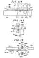
- FIG. 14A and FIG. 14B are diagram showing operations in the device for manufacture of a display device according to the present invention, wherein FIG. 14A is a front view and FIG. 14B is a side view;
- FIG. 15 is a diagram corresponding to FIG. 12 showing the device for manufacture of a display device according to the present invention.
- FIG. 16A and FIG. 16B are diagrams showing the device for manufacture of a display device according to the present invention, wherein FIG. 16A is a front view and FIG. 16B is a side view;
- FIGS. 17A to 17K are diagrams showing a separation step of one example of a scribe roller separation method according to the present invention.
- FIG. 18 is a diagram showing an overall constitutional example of the manufacturing device arranged according to the steps of manufacture of the display device according to the present invention.
- FIG. 19 is a diagram showing an example of forming scribe lines in a conventional scribing and breaking method
- FIGS. 20A to 20C are diagrams showing the operations for separating stacked mother substrates in which scribe lines are formed into display device substrate-units by breaking;
- FIG. 21 is a diagram showing breaking of intermediate wastage portions in FIG. 13 in view of an example of display device substrate-units using a scribing and breaking method;
- FIG. 22 is a diagrammatic plan view showing one example of an irregular break produced by a conventional scribing and breaking method
- FIGS. 23A to 23C are diagrams showing examples of typical flaws which occur in the course of handling the substrate in a conventional scribing and breaking method.
- FIGS. 24A to 24C are diagrams which show examples of substrate crack which occur in stacked mother substrates in which scribe lines are formed and difficulty in removal of intermediate wastage.
- FIGS. 1A and 1B illustrate an example of how scribe lines are formed according to the present invention.
- a method of manufacture according to the present invention is applied to a liquid crystal display device as an example.
- Stacked mother substrates PN which will be described in more detail hereinafter, are formed by laminating a pair of substrates SUB 1 , SUB 2 in such a way that they face each other in an opposed manner, and, between these substrates, a plurality of display regions are formed within a main surface.
- the plurality of these display regions are separated from each other by breaking these stacked mother substrates PN through a scribing step and a breaking step, which will be described hereinafter. Due to such operations, a plurality of display devices (display panels) which respectively constitute the above-mentioned display regions are obtained from the stacked mother substrates PN.
- the plurality of respective display regions are formed as a plurality of spaces which are partitioned by a sealing material between a pair of substrates which constitute the stacked mother substrates.
- the plurality of respective display regions are formed as a plurality of respective evacuated spaces which are partitioned by flit glass between the pair of substrates and are evacuated. In this manner, the operation to form the plurality of display regions between the pair of substrates and to laminate the pair of substrates while arranging them to face each other in an opposed manner is performed as a pre-step in the manufacture of the display device.
- the method of manufacture of the liquid crystal display device is also applicable to a one drop fill method in which liquid crystal composition is preliminarily dropped to a plurality of display regions (portions which are expected to become display regions) which are formed by surrounding regions with a sealing material on one of the pair of substrates before laminating the substrates in the pre-step, and, thereafter, the liquid crystal composition is sealed between the substrates for respective display regions by laminating the pair of substrates.
- FIG. 1A shows one example of the stacked mother substrates which are to be broken into individual display devices (display panels PNL) by the manufacturing method according to this embodiment and one example of the arrangement of the plurality of display regions formed in the main surface
- FIG. 1B shows one display device PNL cut out from the stacked mother substrates PN shown in FIG. 1A .
- a plurality of display regions are formed on the main surface of one of two glass substrates SUB 1 , SUB 2 prepared as mother glasses and these two glass substrates are laminated to each other by arranging a main surface of the other glass substrate to face this main surface in an opposed manner.
- a main surface of the other glass substrate As shown in side views along the x direction and the y direction of the stacked mother substrate PN shown in the lower side and the left side of FIG.
- two glass substrates SUB 1 , SUB 2 which constitute the stacked mother substrate PN are laminated in a state in which these glass substrates SUB 1 , SUB 2 have substantially an equal main surface area (including processing tolerance) and respective end portions are aligned with each other.
- each display region is formed as a region which is surrounded by a pair of scribe lines SBL 1 which extend in the x direction and a pair of scribe lines SBL 2 which extend in the y direction, which intersects the x direction among the scribe lines SBL 1 , SBL 2 which are respectively formed on the main surfaces of the two substrates (glass substrates) SUB 1 , SUB 2 which constitute the stacked mother substrates PN in the scribing step applied to the stacked mother substrates PN.
- the display regions PNL which are cut out as individual display panels are also referred to as display device substrate-units in the explanation provided hereinafter. Further, regions of end portion sides outside the scribe lines SBL 1 , SBL 2 of the glass substrates SUB 1 , SUB 2 are thrown away as wastage.
- X-y coordinates in FIG. 1A indicate that the main surface of the stacked mother substrate PN is formed along a x-y plane.
- the x-y plane extends such that the plane intersects the direction of gravity.
- the stacked mother substrates PN are arranged on a working table or are transported such that the main surface is formed along the x-y plane.
- a device for manufacture of the display device according to the present invention raises the main surface of the stacked mother substrates PN in such a state along the direction of gravity and, thereafter, performs the scribing step and the breaking step sequentially.
- the stacked mother substrates PN may be raised such that the main surface becomes parallel to the direction of gravity (in the vertical direction with respect to the above-mentioned x-y plane), it is preferable to incline the stacked mother substrates PN with a slight angle with respect to the direction of the gravity.
- the stacked mother substrates PN are raised such that the angle which the main surface makes with respect to the direction of gravity becomes smaller compared to a point of time in which the stacked mother substrates are assembled (at the time of finishing of the pre-stage) or at a point of time in which the stacked mother substrates are transported to the manufacturing device according to the present invention and, thereafter, scribes are applied to the main surface. Accordingly, in the manufacturing method of this embodiment, on the main surface of the stacked mother substrates PN, which lie within the x-y plane shown in FIG. 1A , the scribe lines SBL 1 , SBL 2 which are shown in the drawing are not actually formed. In FIG. 1A , these scribe lines SBL 1 , SBL 2 are indicated only for reference purpose to explain respective definitions described hereinafter.
- the stacked mother substrates PN have the main surface thereof raised in the direction of gravity, as described above, and, thereafter, are inclined to the scribe table. In this state, the scribing step of the stacked mother substrates PN is started.
- the scribe lines SBL 1 are formed on the main surface of the first substrate SUB 1 which constitutes the stacked mother substrates PN (an outer surface which also constitutes one main surface of the stacked mother substrates PN at a side opposite to the second substrate SUB 2 .
- the scribe lines SBL 1 are formed as “grooves” on the main surface of the first substrate SUB 1 .
- the scribe lines SBL 1 are formed as “grooves” having a depth which can not break the second substrate SUB 2 .
- the “grooves” of the scribe lines SBL 1 formed in the main surface of the first substrate SUB 1 reach the other main surface of the first substrate SUB 1 in the succeeding breaking step, and the first substrate SUB 1 is broken at given positions (positions where the scribe lines SBL 1 are formed).
- the “grooves” of the scribe lines SBL 2 formed on the main surface of the second substrate SUB 2 also reach the other main surface of the second substrate SUB 2 in the succeeding breaking step, and, hence, the second substrate SUB 2 is broken at given positions (positions where the scribe lines SBL 2 are formed).
- the plurality of display device substrate-units PNL which are formed along the main surface of the stacked mother substrates PN are separated from other neighboring display device substrate-units PNL or the wastages by breaking the first substrate SUB 1 in the breaking step which cleaves the scribe lines SBL 1 and by breaking the second substrate SUB 2 in the breaking step which cleaves the scribe lines SBL 2 .
- the display device substrate-units PNL are formed such that three respective display device substrate-units PNL are arranged along the X direction (long side) in parallel and the Y direction (short side) in parallel, while a periphery (four sides) of the stacked mother substrates PN are thrown away as wastage. Accordingly, in the process for cutting out nine display device substrate-units PNL in total from the stacked mother substrates PN, in the first substrate SUB 1 , eight scribe lines SBL 1 are formed of four scribe lines SBL 1 which extend in the X direction and four scribe lines SBL 1 which extend in the Y direction.
- eight scribe lines SBL 2 are formed of four scribe lines SBL 2 which extend in the X direction and four scribe lines SBL 2 which extend in the Y direction.
- eight scribe lines which extend either the X direction or the Y direction are sequentially formed on the first substrate SUB 1 and the second substrate SUB 2 , these grooves are cleaved in the breaking step to break the stacked mother substrates PN into respective stacked mother substrates PN each of which includes three display device substrate-units PNL.
- the broken stacked mother substrates PN which are formed in the above-mentioned manner are rotated by 90° within the main surface, for example, and, thereafter, the eight remaining scribe lines SBL 1 , SBL 2 which extend in either the Y direction or the X direction are sequentially formed on the broken stacked mother substrates PN and these grooves are cleaved in the breaking step, thus obtaining three display device substrate-units PNL.
- the cut-out individual display device substrate-unit PNL is processed such that either one of the first substrate SUB 1 and the second SUB 2 which are contained in the cut-out individual display device substrate-unit PNL partially projects from the other substrate.
- terminals which receive signals and power needed for driving the display device or integrated circuit elements which drive the display device upon receiving the signals and power are mounted. Accordingly, the portion of either one of the first substrate SUB 1 and the second substrate SUB 2 which projects from the other substrate is referred to as a terminal region, compared to a display region which is formed between these substrates.
- the division of the stacked mother substrates PN and the cutout of display device substrate-units PNL from the broken stacked mother substrates are performed in a state in which the main surface of the first substrate SUB 1 (or the second substrate SUB 2 ) is raised in the direction of gravity, and, hence, the processing which makes one of the first substrate SUB 1 and the second substrate SUB 2 project from the other substrate on the display device substrate-unit PNL can be performed in substantially the same state.
- the processing which separates, by cutting, the periphery along two sides of the second substrate SUB 2 from the display device substrate-unit PNL shown in FIG. 1B and forms the peripheries of the first substrate SUB 1 along two sides is performed in the following manner.
- one of two scribe lines SBL 2 ′ which are shown in FIG. 1B are formed on the main surface of the second substrate SUB 2 , the groove is cleaved in a breaking step thus cutting off one periphery of the second substrate SUB 2 along two sides.
- the display device substrate-unit PNL is rotated by 90°, for example, within the main surface of the first substrate SUB 1 (or the second substrate SUB 2 ).
- the other scribe lines SBL 2 ′ are formed on the main surface of the second substrate SUB 2 and the grooves are cleaved in a breaking step thus separating by cutting a residual (another) portion of the periphery of the second substrate SUB 2 along two sides.
- the scribe lines which extend in the first direction are formed on the main surface of the stacked mother substrates PN, and, thereafter, without forming the scribe lines which extend in the second direction which crosses the first direction, the stacked mother substrates PN are broken in the breaking step in which the grooves formed by the scribe lines which extend in the first direction are sequentially cleaved. Accordingly, the application of a load to the stacked mother substrates PN attributed to the formation of a large number of scribe lines can be reduced.
- the series of the steps of this embodiment can be performed without turning over the stacked mother substrates PN (without changing the position of two laminated substrates) also becomes a factor to suppress the occurrence of cracks.
- the wastage an internal wastage which is produced by the separation of the extra portions can be easily removed from the display device.
- FIG. 1B compared to the conventional technique in which twenty scribed lines in total are formed on both surfaces of the stacked mother substrates PN and the individual display devices are cut out by applying pressure to the stacked mother substrates PN from both sides, according to the technique of this embodiment, it is possible to surely cut out a plurality of display device substrate-units (display regions) PNL formed on the stacked mother substrates PN as display devices.
- the manufacturing method according to this embodiment will be explained more specifically with respect to the respective steps of division of the stacked mother substrates PN and the separation by cutting of the extra portions of the substrate from the display device substrate-units PNL in conjunction with FIGS. 2A to 21 and FIGS. 3A to 3E .
- FIGS. 2A to 2I illustrate the breaking of the stacked mother substrates PN by showing a series of steps for separating, by cutting, the wastage from the periphery of the stacked mother substrates PN, as an example.
- FIG. 2A shows the device prepared for the step and also shows the stacked mother substrates PN which are transported to the device in a state in which the stacked mother substrates PN is raised in the direction of gravity.
- the wastage peripheral wastage
- the stacked mother substrates PN include the first substrate SUB 1 and the second substrate SUB 2 which are overlapped relative to each other and a plurality of display regions AR 1 , AR 2 are formed therebetween.
- the respective display regions are constituted of spaces in which liquid crystal composition is filled. Alternatively, liquid crystal composition supplied according to a one drop fill method is sealed in the space. Further, around the respective display regions AR 1 , AR 2 , walls formed of sealing material are formed such that these walls surround the display regions AR 1 , AR 2 whereby the first substrate SUB 1 and the second substrate SUB 2 are laminated to each other. Accordingly, the stacked mother substrates PN shown in FIG. 2A are depicted from the same viewpoint of any one of the side views of the stacked mother substrates PN shown in FIG.
- the stacked mother substrates PN shown in FIG. 2A are raised in the direction of gravity, and, hence, the main surface of the stacked mother substrates PN (the main surface of the first substrate SUB 1 or the second substrate SUB 2 ) is formed along the x-z plane of the coordinate axes shown in the drawing.
- the reason why the coordinate axes shown in FIG. 2A are described using small letters x, y, z compared to the coordinate axes shown in FIG. 1A , which is described using capital letters X, Y is that the z axis is slightly inclined in the direction of gravity.
- the z axis is inclined with respect to the direction of gravity within a range of 5 to 10°, the z axis may be inclined at an angle which is outside the range in response to the performance of the device shown in FIG. 2A .
- the device shown in FIG. 2A includes surface tables FBS 1 , FBS 2 , a camera TVC which monitors the position of the stacked mother substrates PN, first holding members HB 1 , HB 2 which sandwich the stacked mother substrates PN from both sides, scribe wheels SWH 1 , SWH 2 which form the scribe lines on respective main surfaces of the stacked mother substrates PN, and second holding members BB 1 , BB 2 which sandwich the stacked mother substrates PN from both sides at a side opposite to the scribe wheels SWH 1 , SWH 2 .
- the belt conveyer is interrupted between the surface tables FBS 1 , FBS 2 on which the first holding members HB 1 , HB 2 , the scribe wheels SWH 1 , SWH 2 and second holding members BB 1 , BB 2 which are in charge of the scribing step and breaking step of the stacked mother substrates PN are arranged.
- respective first holding members HB 1 , HB 2 and respective second holding members BB 1 , BB 2 having the rectangular shape shown in FIG. 2A
- the sides thereof which face the first substrate SUB 1 and the second substrate SUB 2 extend in the z axis direction and form surfaces which are brought into contact with the main surfaces of the first substrate SUB 1 and the second substrate SUB 2 .
- these holding members are formed in a “bar” shape which is elongated along a x-z plane.
- the first holding members HB 1 , HB 2 are referred to as holding bars and are also referred to as the bending bars or breaking bars and the second holding members BB 1 , BB 2 are referred to as bending bars or breaking bars.
- the scribe wheels SWH 1 , SWH 2 which are arranged between the first holding members HB 1 , HB 2 and the second holding members BB 1 , BB 2 , a known scribe wheel having a blade on a circumference thereof is used.
- the above-mentioned device shown in FIG. 2A is, in view of the functions thereof, referred to as a scribing and breaking device hereinafter.
- the scribing step and the breaking step applied to the first substrate SUB 1 and the scribing step and the breaking step applied to the second substrate SUB 2 are sequentially performed.
- the first holding member (holding bar) HB 1 and the second holding member (bending bar) BB 1 are brought into pressure contact with the main surface (outer main surface) of the first substrate SUB 1
- the second holding member HB 2 and the second holding member BB 2 are brought into pressure contact with the main surface (outer main surface) of the second substrate SUB 2 so as to fix the position of the portions of the stacked mother substrates PN to be worked with respect to the scribe wheels SWH 1
- the scribe wheel SWH 1 is arranged close to the main surface of the first substrate SUB 1 along the y axis.
- the scribe wheel SWH 1 When the scribe wheel SWH 1 starts to move in the z axis direction while being brought into contact with the main surface of the first substrate SUB 1 , the blade which is formed in the circumference of the scribe wheel SWH 1 is rotated to cut into the main surface of the first substrate SUB 1 .
- a rotary shaft of the scribe wheel SWH 1 When a rotary shaft of the scribe wheel SWH 1 is moved in the z axis direction in such a state, the scribe line (groove) which extends in the z axis direction is formed in the first substrate SUB 1 .
- the first holding member, the scribe wheel and the second holding member which are indicated by a broken line in FIG. 2B represent respective positions in the immediately-before step (step shown in FIG. 2A with respect to step shown in FIG. 2B ).
- the step shown in FIG. 2C is started.
- the scribe wheel SWH 1 is separated from the main surface of the first substrate SUB 1 and, thereafter, the first holding member HB 1 and the second holding member BB 1 are shifted toward the scribe line SBL 1 along the x direction.
- the first holding member HB 1 and the second holding member BB 1 are first separated from the first substrate SUB 1 and are moved along the x axis and, thereafter, are brought into pressure contact with the main surface of the first substrate SUB 1 .
- the first holding member HB 2 and the second holding member BB 2 at the second substrate SUB 2 side are shifted toward the scribe line SBL 1 in the same manner.
- the second holding members BB 1 , BB 2 which sandwich the stacked mother substrates PN are rotated in the x-y plane to warp the stacked mother substrates PN such that a side A and a side B which sandwich the scribe line SBL 1 on the main surface at the second substrate SUB 2 side assumes an angle ⁇ 1 which is less than 180°.
- the first holding members HB 1 , HB 2 are hardly moved as shown in the drawing.
- the stacked mother substrates PN are bent toward the side opposite to the main surface on which the scribe line SBL 1 is formed and the main surface (at the first substrate SUB 1 side) on which the scribe line SBL 1 is formed assumes an angle which exceeds 180° at both sides of the center (indicated by a chain line CSL 1 ) of the scribe line SBL 1 .
- the main surface of the first substrate SUB 1 is warped at a portion where the scribe line SBL 1 is formed, the groove which is formed in the first substrate SUB 1 as the scribe line SBL 1 is cleaved in the thickness direction of the first substrate SUB 1 , thus forming a break portion BRL 1 . Since the first substrate SUB 1 is broken in the z axis direction while tracing a locus of the scribe line SBL 1 , the break portion BRL 1 is also referred to as a break line.
- the first holding members HB 1 , HB 2 and the second holding members BB 1 , BB 2 are separated from the stacked mother substrates PN as shown in FIG. 2E and return to the positions shown in FIG. 2A once together with the scribe wheels SWH 1 , SWH 2 .
- scribing of the second substrate SUB 2 is started.
- a series of steps ranging from the step shown in FIG. 2B to the step shown in FIG. 2D may be repeated by replacing the operation of the scribing wheel SWH 1 in the step shown in FIG. 2B with the operation of the scribing wheel SWH 2 and by upwardly warping the main surface of the second substrate SUB 2 shown in FIG. 2D at the portion where the scribe line is formed.
- the explanation is made with respect to a series of steps in which the second substrate SUB 2 is cut at a position different from the position of the first substrate SUB 1 and an end portion of the second substrate SUB 2 projects from the first substrate SUB 1 .
- the first holding member HB 1 and the second holding member BB 1 are brought into pressure contact with the main surface of the first substrate SUB 1
- the first holding member HB 2 and the second holding member BB 2 are brought into pressure contact with the main surface of the second substrate SUB 2 so as to fix the position of the portions of the stacked mother substrates PN to be worked with respect to the scribe wheels SWH 2 . Since the portion to be worked is shifted in the x direction relative to the position explained in conjunction with the step shown in FIG.
- both of the portion of the stacked mother substrates PN which is sandwiched by the first holding members HB 1 , HB 2 and the portion of the stacked mother substrates PN which is sandwiched by the second holding members BB 1 , BB 2 are shifted in the x direction compared to corresponding portions in FIG. 2B .
- the scribe wheel SWH 2 is made to approach the main surface of the second substrate SUB 2 along the y axis while being rotated.
- the rotary shaft is moved in the z axis direction.
- the step shown in FIG. 2G is started.
- the scribe wheel SWH 2 is separated from the main surface of the second substrate SUB 2 and, thereafter, the first holding member HB 2 and the second holding member BB 2 are shifted toward the scribe line SBL 2 along the x axis.
- the first holding member HB 1 and the second holding member BB 1 which are brought into pressure contact with the main surface of the first substrate SUB 1 , are also shifted toward the scribe line SBL 2 in the same manner. In the same manner as FIG.
- these holding members are first separated respectively from stacked mother substrates PN and are moved along the x axis direction.
- the first holding member HB 1 is brought into pressure contact with the first substrate SUB 1 at a position where the first holding member HB 1 covers the break portion BRL 1 .
- first holding member HB 2 is arranged to face the first holding member HB 1 in an opposed manner and is brought into pressure contact with the main surface of the second substrate SUB 2 so as to reinforce the strength of the portion of the first substrate SUB 1 where the break portion BRL 1 is formed from the second substrate SUB 2 side.
- the second holding members BB 1 , BB 2 which sandwich the stacked mother substrates PN are rotated in the x-y plane to warp the stacked mother substrates PN such that a side A′ and a side B′ which sandwich the scribe line SBL 1 on the main surface of the stacked mother substrates PN at the first substrate SUB 1 side assumes an angle ⁇ 2 which is less than 180°.
- the first holding members HB 1 , HB 2 are hardly moved, as shown in the drawing.
- the main surface of the second substrate SUB 2 assumes an angle which exceeds 180° at both sides of the center (indicated by a chain line CSL 2 ) of the scribe line SBL 2 .
- the groove which is formed in the second substrate SUB 2 as the scribe line SBL 2 is cleaved in the thickness direction of the second substrate SUB 2 , thus forming a break portion BRL 2 .
- the break portion BRL 2 is also used for breaking the second substrate SUB 2 in the z axis direction while tracing a locus of the scribe line SBL 2 .
- one (HB 1 ) of the first holding members is brought into pressure contact with the break portion BRL 1 on the main surface (outer main surface) of the first substrate SUB 1 and the periphery thereof and the other (HB 2 ) of the first holding members is brought into pressure contact with a region (on which the break portion BRL 1 is projected) of the main surface (outer main surface) of the second substrate SUB 2 which faces the break portion BRL 1 and the periphery thereof. Accordingly, the movement of the end portion (side B) of the first substrate SUB 1 which is caused by bending of the second substrate SUB 2 can be suppressed.
- the separated sub stacked mother substrates PN when so-called sub stacked mother substrates PN including M pieces (M being a natural number and N>M>1) of display device substrate-units PNL are separated from the stacked mother substrates PN on which N pieces of display device substrate-units PNL are formed, the broken sub stacked mother substrates PN are shown at the right side of FIG. 2H .
- the separated sub stacked mother substrates PN extend toward the right end of FIG. 2H along the x axis direction, and, hence, when the separated sub stacked mother substrates PN are separated by cutting from the body of the stacked mother substrates PN in the step shown in FIG. 2I , the separated sub stacked mother substrates PN are transferred in the x axis direction by a belt conveyor which is provided along the surface table FBS 2 .
- the stacked mother substrates PN shown in FIG. 2I have a shape where a portion (the end portion) of the stacked mother substrates PN is separated by cutting as wastage or the sub stacked mother substrates PN.
- the stacked mother substrates PN are shifted along the x axis as indicated by an arrow such that portions of the first substrate SUB 1 and the second substrate SUB 2 to be cut next enter the work area of the scribing and breaking device and are again stopped at a desired position.
- the stacked mother substrates PN are transferred from the belt conveyer which is arranged along the surface table FBS 1 to the belt conveyer which is arranged along the surface table FBS 2 .
- FIG. 2A to FIG. 2I show, performed in a state in which the main surface (of the first substrate SUB 1 and the second substrate SUB 2 ) of the stacked mother substrates PN is arranged along the x-z plane.
- the stacked mother substrates PN including the end portion to be cut maintains a state in which the stacked mother substrates PN are raised in the direction of gravity. Accordingly, the deflection of the stacked mother substrates PN due to their own weight can be suppressed whereby unpredicted substrate cracks which occur from the scribe lines or the like can be suppressed.
- the stacked mother substrates PN which are inserted into the work region of the scribing and breaking device in the step shown in FIG. 2A is not transported until the scribing step and the breaking step which are applied to the first substrate SUB 1 and the second substrate SUB 2 , respectively, are finished (step shown in FIG. 2I ). Accordingly, the positions of the first substrate SUB 1 and the second substrate SUB 2 in the scribing and breaking device are not changed during the period ranging from the step shown in FIG. 2A to the step shown in FIG. 2I except for the slight movement of respective end portions which are bent in the steps shown in FIG. 2D and FIG. 2H .
- the first substrate SUB 1 is held at the same position from the point of time that the scribe line SBL 1 is formed on the first substrate SUB 1 to the point of time that the first substrate SUB 1 is broken along the scribe line SBL 1 .
- the second substrate SUB 2 is also held at the same position from the point of time that the scribe line SBL 2 is formed on the second substrate SUB 2 to the point of time that the second substrate SUB 2 is broken along the scribe line SBL 2 .
- the scribing step and the breaking step to the first substrate SUB 1 and the second substrate SUB 2 respectively without inverting the stacked mother substrate PN.
- the relationship in which the first substrate SUB 1 faces the surface table FBS 1 in an opposed manner at the point of time that the stacked mother substrates PN are transported to the scribing and breaking device is maintained until the scribing step and the breaking step which are applied to the first substrate SUB 1 and the second substrate SUB 2 are finished, and there is no possibility that the second substrate SUB 2 faces the surface table FBS 1 in place of the first substrate SUB 1 in the midst thereof.
- the reason why the scribing step and the breaking step of the stacked mother substrates PN can be performed without changing the position of the stacked mother substrates PN (in a so-called shift-free state) and without inverting the stacked mother substrates PN (in a so-called inversion-less state) in the above-mentioned manner lies in the breaking step which bends the stacked mother substrates PN on which the scribe lines are formed. It is preferable to perform this breaking step by bending the stacked mother substrates PN for every scribing step (for every scribe line).
- the plane on which the first holding members and the second holding members move around extends along the transfer direction (x axis) of the stacked mother substrates PN and preferably extends in parallel to the transporting direction of the stacked mother substrates PN. It is preferable that the plane is orthogonal to the main surface of the stacked mother substrates PN.
- the respective substrates SUB 1 , SUB 2 are broken (separated) by bending the stacked mother substrates PN and the substrates which are scribed for every scribing step are broken using the subscribe wheels SWH 1 , SWH 2 which are arranged between the first holding members HB 1 , HB 2 and the second holding members BB 1 BB 2 .
- the above-mentioned translational motion of the holding members indicates a so-called linear motion of the above-mentioned holding members and is exemplified as a motion which moves the rectangular holding members shown in FIG. 2A such that the four corners draw loci which are parallel to each other.
- the above-mentioned rotational motion of the holding members is exemplified as a motion which inclines the respective other ends (the right side) of the second holding members BB 1 , BB 2 shown in FIG. 2D and FIG. 2H in the y-axis direction with respect to respective ends (the left side) of the second holding members BB 1 , BB 2 which are brought into contact with the substrates SUB 1 , SUB 2 (the rotation of the second holding members about one end thereof.
- the above-mentioned breaking step in which the stacked mother substrates PN are broken by bending can be also performed by a translational motion and a rotational motion of the first holding members HB 1 , HB 2 within the above-mentioned plane (x-y plane) and a translational motion of the second holding members BB 1 , BB 2 within the above-mentioned plane (x-y plane). Further, the translation motion and the rotational motion may be imparted to the first holding members HB 1 , HB 2 and the second holding members BB 1 , BB 2 within the above-mentioned plane (x-y plane of the scribing and breaking device).
- the technique which juxtaposes the first holding members and the second holding members which sandwich the workpiece along the transporting direction of the workpiece in the scribing and breaking device and performs the breaking step of the workpiece by translational motion and rotational motion of the first holding members and the second holding members on the plane which intersects the main surface (working surface) of the workpiece and are arranged along the transporting direction of the workpiece is also applicable to a scribing and breaking device which transports the workpiece such that a main surface thereof is directed in a direction (horizontal direction) which is orthogonal to the direction of gravity and can obtain an advantageous effect in that the workpiece can be broken without deflecting the workpiece.
- the scribing and breaking device described in connection with this embodiment is applicable to other manufacturing devices which do not raise the workpiece (stacked mother substrates PN) as a component technique in the direction of gravity.
- the stacked mother substrates PN shown in FIG. 1A are broken into sub stacked mother substrates, each of which includes three display device substrate-units PNL and the wastage in response to a group of scribe lines SBL 1 , SBL 2 (four scribe lines SBL 1 and four scribe lines SBL 2 ), which extend either in the X direction or in the Y direction among four scribe lines SBL 1 formed on the first substrate SUB 1 and eight scribe lines SBL 2 formed on the second substrate SUB 2 .
- the scribing step and the breaking step which have been described in conjunction with FIG. 2A to FIG. 2I are applicable to the step of cutting out the display device substrate-units PNL from the sub stacked mother substrates PN.
- FIG. 3A shows the general configuration of one example of a scribing and breaking device used in the series of steps such that the scribe lines are formed on one (first substrate SUB 1 ) of the pair of substrates which constitute the display device substrate-units PNL. Accordingly, the first holding members (holding bars) HB 1 , HB 2 and the second holding members (holding bars) BB 1 , BB 2 indicated by a solid line in FIG. 3A are respectively brought into pressure contact with the main surfaces of the first substrate SUB 1 and the second substrate SUB 2 in the same manner as FIG. 2B for preparing the formation of the scribe lines on the main surface of the first substrate SUB 1 using the scribe wheel SWH 1 .
- the respective structures and respective functions of the first holding members HB 1 , HB 2 , the scribe wheels SWH 1 , SWH 2 , the second holding members BB 1 , BB 2 , the surface tables FBS 1 and the camera TVC which are provided to the scribing and breaking device are common with respective constitutional components shown in FIG. 2B .
- a belt conveyor not shown in FIG. 3A is provided along the surface table FBS 1 and a workpiece (display device substrate-units PNL) is transported along the x axis direction based on positional information on the workpiece obtained from the camera TVC.
- 3A is provided with a substrate rotary machine ROT having a stage STG which comes into contact with one main surface of the workpiece (display device substrate-units PNL).
- the substrate rotary machine ROT imparts an air chuck function to the stage STG.
- the substrate rotary machine ROT causes the stage STG to suck the main surface of the workpiece and rotates the workpiece within the main surface (x-z plane defined by coordinates shown in FIG. 3A ).
- This function is useful in an operation to separate the peripheries of the substrate SUB 2 of the display device substrate-units PNL shown in FIG. 1B by cutting along the scribe lines SBL 2 ′ which are drawn along two neighboring sides respectively.
- An operation to form the scribe lines on the main surface of the first substrate SUB 1 in the step shown in FIG. 3A is performed in the same manner as the above-mentioned step shown in FIG. 2B .
- the operation in the step shown in FIG. 3B which follows the step shown in FIG. 3A that is, the operation to maintain the workpiece (display device substrate-units PNL) while shifting the first holding members HB 1 , HB 2 and the second holding members BB 1 , BB 2 toward the scribe lines SBL 1 is performed in the same manner as the step shown in FIG. 2C . Further, the step shown in FIG.
- FIG. 3A The operation peculiar to the scribing and breaking device shown in FIG. 3A appears in steps shown in FIG. 3D and FIG. 3E which succeed the step shown in FIG. 3C .
- steps shown in FIG. 3D and FIG. 3E which succeed the step shown in FIG. 3C .
- one holding member BB 1 which is brought into contact with the first substrate SUB 1 is, as shown in FIG. 3D , rotated in the clockwise direction about another end (right end) of a surface which opposingly faces the first substrate SUB 1 .
- another holding member BB 2 which is brought into contact with the second substrate SUB 2 is rotated in the counter clockwise direction about one end (left end on a surface which opposingly faces the second substrate SUB 2 ) which is brought into contact with the second substrate SUB 2 , and returns to the position shown in FIG. 3B .
- the second substrate SUB 2 which is deflected in the y axis direction in the step shown in FIG. 3C is pushed by the second holding member BB 2 such that an angle ⁇ 1 which is made between the side A and the side B returns to ⁇ (180°).
- the side B of the first substrate SUB 1 shown in FIG. 3D is separated from the side A and is formed into the wastage WT 1 due to the breaking step shown in FIG. 3C .
- a material having adhesiveness such as a sealing agent or flit glass which laminates the first substrate SUB 1 and the second substrates SUB 2 is supplied to the main surface of the first substrate SUB 1 while avoiding the region which becomes the wastage WT, there exists a possibility that the adhesive material projects also to a region which constitutes the wastage WT in an actual operation.
- the second holding member BB 1 which is brought into contact with the first substrate SUB 1 (side B which is formed into the wastage WT 1 ) is rotated to be inclined with respect to the main surface of the second substrate SUB 2 and, at the same time, the second substrate SUB 2 (the side B which is brought into contact with the wastage WT 1 ) is pushed toward the first substrate SUB 1 using the second holding member BB 2 , whereby it is possible to make the wastage WT 1 float from the contact surface with the workpiece, wherein the wastage WT 1 is difficult to peel off from the workpiece (display device substrate-unit PNL) even when the wastage WT 1 is cut out from the first substrate SUB 1 (side A).
- the first holding members HB 1 , HB 2 and the second holding members BB 1 , BB 2 return, as shown in FIG. 3E to respective standby positions (indicated by dotted lines in FIG. 3A ).
- a stage STG of a substrate rotating machine ROT is brought into contact with the main surface (main surface of the second substrate SUB 2 ) and the workpiece is rotated within the main surface (x-z plane).
- the scribing and breaking device shown in FIG. 3A is, compared to the scribing and breaking device shown in FIG. 2A , characterized in that the center of rotational motion of the second holding member BB 1 on the plane which intersects the main surface of the workpiece and is arranged along the transport direction of the workpiece can be changed.
- This scribing and breaking device can be used also in the division of the stacked mother substrates PN and the separation of the display device substrate-units PNL from the (broken) stacked mother substrates.
- the embodiment 1 was specifically directed to the method of manufacture of the display device according to the present invention in which the scribing step and the breaking step of the stacked mother substrates PN are performed in a state in which the stacked mother substrates PN are held in a shift-free and inversion-less mode and in a state that the stacked mother substrates PN is broken by bending.
- the embodiment 2 is directed to a manufacturing method which shifts stacked mother substrates PN between a scribing step and a breaking step. This embodiment 2 will be described hereinafter in conjunction with FIGS. 4A to 4G and 5 A to 5 G.
- the stacked mother substrates PN and display device substrate-units obtained by breaking the stacked mother substrates PN are transported and processed in such a state that the stacked mother substrates PN and the display device substrate-units are raised along the direction of gravity.
- the breaking step which clamps the both sides of the portion of a main surface of a workpiece (substrates) on which a scribe line (groove) is formed using bar-like holding members and bends the workpiece by applying the rotational motion to one side of the portion within a surface which intersects the main surface of the substrate is substantially common with the breaking step described in the embodiment 1.
- FIGS. 4A to 4G are diagrams which show the operation in which the stacked mother substrates are separated into individual display device substrate-units in the embodiment 2.
- the stacked mother substrates having four (2 ⁇ 2) display device substrate-units will be taken as an example.
- the stacked mother substrates PN on which the scribe lines SBL 12 and the SBL 22 extending in the long-side direction are simultaneously formed are transported to the long-side breaking position.
- the stacked mother substrates PN are separated into the individual display device substrate-units.
- the peripheral wastages WT 3 , WT 4 are thrown away.
- the display device substrate-units are transported to the display device substrate-unit intermediate wastage break position.
- the removed portions of the second substrates SUB 2 do not constitute intermediate wastages.
- these portions are referred to as the intermediate wastages.
- FIGS. 5A to 5G are diagrams which show the operation in which the intermediate wastages are separated from the display device substrate-units which are separated by the process shown in FIGS. 4A to 4G .
- the intermediate wastage portions are the peripheral portions close to the second substrate SUB 2 shown in FIG. 1B .
- a scribe line SBL 3 is formed on one of short sides of the second substrate SUB 2 of the display device substrate-unit PNL.
- a scribe line SBL 4 is formed on one of the long sides of the second substrate SUB 2 .
- the display device substrate-unit PNL having whole scribe lines formed thereon are transported to a breaking position.
- FIG. 6 is an explanatory view of the substrate transportation and the inverting operation of a working surface of a manufacturing device according to the present invention which separates the stacked mother substrates into the display device substrate-units by forming scribe lines on the stacked mother substrates and by breaking the stacked mother substrates.
- FIG. 6 is an explanatory view of the substrate transportation and the inverting operation of a working surface of a manufacturing device according to the present invention which separates the stacked mother substrates into the display device substrate-units by forming scribe lines on the stacked mother substrates and by breaking the stacked mother substrates.
- a scribe table SBT of a scribe forming machine which performs forming of scribe lines
- an inverting table RT 1 which performs the inversion (changing of an inclined angle) of a working surface of the substrate
- a breaking table BKT of a break forming machine and an inverse reception table RT 2 which performs reception of substrates when the working surface is inverted face each other with the vertical direction sandwiched therebetween and in the vicinity of the vertical direction (an angle inclined by 5 to 10° to the opposite side with respect to the vertical direction).
- the scribe table SBT, the inverse table RT 1 , the inverse reception table RT 2 , the break table BKT are arranged in this order of the scribe table SBT, the inverse table RT 1 , the inverse reception table RT 2 , the break table BKT from the upper stream side.
- belt conveyers having an inclination substantially equal to the inclination of the respective table surfaces are provided for transporting the stacked mother substrates PN after the scribe lines are formed on the stacked mother substrates PN.
- the belt conveyers COV 1 , COV 3 including an elevating mechanism for elevating the belt conveyers per se are arranged.
- the belt conveyer COV 2 which changes an angle thereof at an inclination angle in synchronism with the inverse table RT 1 is arranged.
- Each table is provided with suction holes which suck air to hold the substrate and blow off air to peel off the substrate and, further, a vacuum suction blow mechanism which is not shown in the drawing is arranged on each table.
- the stacked mother substrates PN are held by suction to the scribe table SBT in a state that the stacked mother substrates PN are raised in the vicinity of the vertical direction. From this state, the belt conveyer COV 1 is elevated and is brought into contact with the lower end of the stacked mother substrates PN. Next, the belt conveyer COV 1 is lowered while making extremely weak air blow from the suction holes formed in the scribe table SBT so as to transfer the stacked mother substrates PN to the belt conveyer COV 1 .
- the belt conveyer COV 1 and the belt conveyer COV 2 are advanced and, at the same time, extremely weak air is blown off from the suction holes formed in the scribe table SBT and the inverse table RT 1 and hence, the substrates PN are transported in a floating state from the respective tables and are transferred to the inverse table RT 1 side.
- the inclination angle of the inverse table RT 1 is changed to a value approximately equal to the inclination angle at the inverse reception table RT 2 side in synchronism with the belt conveyer COV 2 . Then, from this state, the working surface of the substrates PN is turned over by releasing the suction of the inverse table RT 1 and, at the same time, the substrates PN are transferred to the inverse reception table RT 2 side.
- the belt conveyer COV 2 and the belt conveyer COV 3 are advanced and, at the same time, extremely weak air is blown off from the suction holes formed in the inverse reception table RT 2 , the break table BKT and, the substrates PN are transported in a state being floated from the respective tables and transferred to the belt conveyer COV 3 side. Further, after the transfer of the substrates PN is completed, the inclination angles of the belt conveyer COV 2 and the inverse table RT 1 are returned to the original state.
- the belt conveyer COV 3 is elevated and, after the elevation of the belt conveyer COV 3 is completed, the substrates PN are held by suction to the break table BKT and are transferred.
- the belt conveyer COV 3 is lowered to the original position after the suction is completed.
- the substrate transportation using the belt conveyers for example, is replaced by a shuttle method, or the scribe table SBT is directly advanced, changes an angle thereof and is transferred to the break table without using the inverse table or the inverse reception table.
- FIG. 7 to FIG. 9 are diagrams of a substrate breaking and separating device in the manufacturing device of a display device according to the present invention.
- FIG. 7 is a top plan view
- FIG. 8 is a front view of a representative part
- FIG. 9 is a side view of a representative part.
- the stacked mother substrates PN are, after the formation of the scribe lines is completed, transported from an upstream side by belt conveyers and, then, is transferred to a breaking working machine.
- the substrates PN By driving and stopping belt conveyers COV 2 , COV 3 , the substrates PN are moved to an arbitrary separating position.
- the substrates PN which are broken and are separated are transported to a downstream side by the belt conveyer COV.
- the substrates are inclined with an inclination angle of 5 to 10° in the vertical direction to prevent the substrates from falling and, at the same time, air is blown off from suction holes formed in a fixed-side surface table FBS and an angle-changing-side surface table VBS to transport the substrates in a state that the substrates are floated thus preventing the collapsing of the substrate surface.
- fixed-side substrate holding bars BHB, angle-changing-side substrate holding bars VBB are advanced and, in a state that the substrates are sandwiched between the fixed-side surface table FBS and the angle-changing-side surface table VBS respectively, the belt conveyers COV 1 , COV 2 are lowered and retracted. Further, the angle-changing-side surface table VBS is bent for respective angle-changing-side substrate holding bars VBB so as to break the substrates in the direction which applies a tensile strength to the scribe line.
- wastage which is generated in this breaking operation is thrown away into a wastage housing box BX in such a manner that the respective substrate holding bars are retracted in a state that the wastages are sucked to the respective substrate holding bars and the suction of the respective bars is released while blowing off air toward the wastage housing box BX using an air blow nozzle NZ.
- FIGS. 10A to 10F are diagrams which show the substrate breaking and separating process by the manufacturing device shown in FIG. 7 to FIG. 9 . As described above,
- FIG. 11A , FIG. 11B and FIG. 12 are diagrams illustrating another embodiment of a manufacturing method and a manufacturing device according to the present invention.
- FIGS. 11A and 11B are diagrams relating to the manufacturing method
- FIG. 12 is a diagram relating to the manufacturing device and corresponds to FIG. 2B .
- a scribe wheel and a break roller for promoting the cleaving of a scribe line which is formed using the scribe wheel by expanding the scribe line from a side opposite to a side on which the scribe line is formed by pushing are arranged. Then, by moving the scribe wheel and the break roller substantially simultaneously or in such a manner that the break roller follows the scribe wheel in the direction that the above-mentioned workpiece surface is to be separated, it is possible to separate the workpiece by one step.
- FIG. 11A and FIG. 11B are diagrams which show the manufacturing method, wherein FIG. 11A is a front view and FIG. 11B is a side view.
- one surface of a glass plate GP which constitutes a workpiece is scribed by moving the scribe wheel SWH 1 in the direction shown by arrows, and, hence, a scribe line SBL is formed.
- the break roller BRR which is arranged at another surface side while sandwiching the glass plate GP which constitutes the workpiece together with the scribe wheel SWH 1 is brought into a pressure contact with another surface of the glass plate GP. Holding this pressure contact state, the break roller BRR is made to advance in the same direction as the above-mentioned scribe wheel SWH 1 substantially simultaneously with the scribe wheel SWH 1 or following the scribe wheel SWH 1 with a slight delay as shown in the drawing and the cleaving of the above-mentioned scribe line SBL is promoted and is broken thus separating the above-mentioned workpiece by the above-mentioned scribe line SBL.
- FIG. 12 is a diagram showing one example of a manufacturing device according to the present invention which incorporates the break roller BRR in the inside of the device and corresponds to the above-mentioned FIG. 2A .
- the break roller BRR 1 which promotes the cleaving of the scribe line SBL is arranged at a side opposite to the scribe wheel SWH 1 which forms scribe lines on the main surface of the first substrate SUB 1 of the stacked mother substrates PN and, at the same time, between a first holding member HB 2 which sandwiches the stacked mother substrates PN from both sides thereof together with a first holding member HB 1 and a second holding member BB 2 which sandwiches the stacked mother substrates PN from both sides thereof together with a second holding member BB 1 in the same manner as the first holding member HB 2 .
- the break roller BRR 1 is operated in a state that the scribe wheel SWH 1 scribes the stacked mother substrates PN, that is, the break roller BRR 1 is operated in a state that the stacked mother substrates PN is clamped and fixed between the first holding members HB 1 , HB 2 as well as between the second holding members BB 1 , BB 2 and hence, the scribe line formed on the main surface of the first substrate SUB 1 is sequentially pushed from the main surface side of the second substrate SUB 1 whereby the cleaving of the above-mentioned scribe line is enhanced.
- FIG. 13 is a diagram showing another embodiment of a manufacturing method and a manufacturing device according to the present invention.
- This embodiment provides a method and a device which are suitable for separating a workpiece having the laminated structure constituted of the first and second substrates such as the above-mentioned stacked mother substrates PN and is characterized in that both substrates can be broken simultaneously.
- the manufacturing device includes a first scribe wheel SWH 1 which forms a scribe line SBL 5 on a main surface of the first substrate SUB 1 of the stacked mother substrates PN, a first break roller BRR 1 which is arranged on a side opposite to the first scribe wheel SWH 1 while sandwiching the above-mentioned stacked mother substrates PN therebetween and promotes the cleaving of the scribe line SBL 5 which is formed on the main surface of the first substrate SUB 1 , a second scribe wheel SWH 2 which forms a scribe line SBL 6 on a main surface of the second substrate SUB 2 and a second break roller BRR 2 which is arranged on a side opposite to the second scribe wheel SWH 2 while sandwiching the stacked mother substrates PN therebetween and promotes the cleaving of the scribe line SBL 6 which is formed on the main surface of the second substrate SUB 2 . Due to such a constitution, it is possible to separate the first and the second substrates of the stacked mother mother substrates PN
- FIG. 14A , FIG. 14B and FIG. 15 are diagrams showing another embodiment of a manufacturing method and a manufacturing device according to the present invention.
- FIG. 14A and FIG. 14B are views relating to the manufacturing method, wherein FIG. 14A is a front view, FIG. 14B is a side view and FIG. 15 relates to the manufacturing device and corresponds to FIG. 12 .
- This embodiment is directed to a further improvement of the embodiment shown in FIG. 13 in which the operability at the time of performing the scribing operation can be enhanced.
- a scribe wheel SWH 1 for forming a scribe line SBL 5 is arranged on a main surface of a first substrate SUB 1
- a scribe wheel SWH 2 for forming a scribe line SBL 6 is arranged on a main surface of a second substrate SUB 2
- a scribe assist roller SWR 2 is arranged on the main surface side of the substrate SUB 1 to face the scribe wheel SWH 2 in an opposing manner.
- a break assist roller BRR 21 is arranged on a main surface side of the first substrate SUB 1 at a position where the break assist roller BRR 21 faces the break roller BRR in an opposing manner.
- the break roller BRR 2 and the break assist roller BRR 21 are arranged coaxially.
- the reference symbol CHU indicates a substrate breaking unit and has a constitution having a range surrounded by a dotted double-dashed line.
- the substrate breaking unit is a substrate breaking unit of the second substrate SUB 2 .
- the scribe assist roller SWR 2 is a flat roller and this scribe assist roller SWR 2 functions as a reaction force suppressor at the time of scribing using the scribe wheel SWH 2 .
- a concave roller is used as the break assist roller BRR 21 , wherein the break assist roller BRR 21 promotes the progress of cleaving of the scribe line SBL 6 in a cooperative manner with the break roller BRR 2 formed of a convex roller in a pair.
- break roller BRR 2 and the break assist roller BRR 21 are arranged coaxially as described above, it is also possible to control a broken surface shape by shifting the center axes of both rollers.
- the cleaving depth of the scribe formed in the one-side substrate can be made deeper than the cleaving depth of the scribe formed in the other side so as to enhance the reliability of breaking operation.
- FIG. 16A and FIG. 16B are diagrams showing another embodiment of a manufacturing method and a manufacturing device according to the present invention, wherein FIG. 16A is a front view and FIG. 16B is a side view.
- a substrate breaking unit CHU 1 which is used for the first substrate SUB 1 is further added to the constitution of the above-mentioned embodiment 7.
- the reliability of scribing and breaking can be further enhanced.
- FIGS. 17A to 17K show the breaking steps as one example of the scribe roller breaking method according to the present invention explained in the above-mentioned embodiments 5 to 8.
- FIGS. 17A to 17K the embodiment will be explained using a plan view and a side view shown below the plan view.
- scribing is performed using scribe wheels SHW 1 , SHW 2 .
- the cleaving of the scribe lines is enhanced using the break roller so as to break the end portion of the scribe line by a breaking line BKL and the peripheral wastage WT is thrown away.
- a scribe line SBL 7 is formed at a position shown in FIG. 17C on the first substrate SUB 1 .
- the cleaving of the scribe line SBL 7 which is formed on the first substrate SUB 1 is progressed and breaking is performed.
- FIG. 17D at a position away from the scribe line SBL 7 by a width of an intermediate wastage WTM, the both substrates SUB 1 and SUB 2 are broken using a combination of the scribes and the break rollers and display device substrate-units PNL 1 having a terminal portion thereof exposed and the intermediate wastage WTM are separated.
- a scribe line SBL 8 is formed on the remaining portion of the first substrate SUB 1 of the stacked mother substrates PN in FIG. 17E and, simultaneously with or following the step, by applying pressure using the break roller from the second substrate SUB 2 side the scribe line SBL 8 formed on the first substrate SUB 1 is cleaved and broken.
- An end portion WT 5 which is broken at this scribe line SBL 8 and the portion of the second substrate SUB 2 corresponding to the end portion WT 5 are broken again by a size corresponding to a terminal portion in FIG. 17F and a display device substrate-unit PNL 2 having a terminal portion thereof exposed, a peripheral wastage WT 51 and a peripheral wastage WT 52 are separated.
- the long side end portion of the broken display device substrate-unit PNL 6 is broken in FIG. 17J thus obtaining a display device substrate-unit PNL 61 having a terminal portion continuously formed at one long side and one short side. Thereafter, the long side end portion of the display device substrate-unit PNL 61 having no terminal portion is broken and a peripheral wastage WT 8 is thrown away thus obtaining the display device substrate-unit PNL 7 .
- FIG. 18 is a diagram showing an example of the overall constitution of the manufacturing device arranged according to the steps of manufacture of a display device according to the present invention.
- An upper stage of the drawing shows the arrangement constitution of the device and a lower stage of the drawing shows the shape of substrates at respective steps.
- the symbol LD indicates a transported position and large-sized stacked mother substrates PN are transported using a cassette loader.
- the transported stacked mother substrates PN are transferred to a substrate raising machine VS by a horizontal multi-articulated robot RBT 1 and are raised on the table surface of the large-sized substrate ⁇ strip-like scribe/break device MSC.
- Symbol TFU indicates a substrate transporting unit formed of the above-mentioned conveyers
- symbol SBT indicates a surface table
- symbol SB/BK 1 indicates a scribing and breaking unit for the first substrate
- symbol SB/BK 2 indicates a scribing and breaking unit for the second substrate.
- a substrate rotating unit SPR is arranged in the downstream of the large-sized substrate ⁇ strip-like scribe/break device MSC.
- Symbol TT indicates a substrate rotating table
- symbol RR indicates a rotating mechanism.
- the substrates which are broken into strips using the large-sized substrate ⁇ strip-like scribe/break device MSC are transferred to a strip ⁇ display device substrate-unit scribe/break device SPC having the substantially same constitution as the large-sized substrate ⁇ strip-like scribe/break device MSC and having a processing size corresponding to the strip-like substrates.
- the substrates (display device substrate-units) which are separated into the display device substrate-units using the strip ⁇ display device substrate-unit scribe/break device SPC are transferred to a scribing and breaking device for terminal portion wastages, that is, intermediate wastages WTC and the intermediate wastages are separated in the manner as described above.
- the intermediate wastage scribing and breaking device WTC has the constitution which performs the scribing and breaking on the second substrate only and the scribe line forming and breaking processing have constitutions which are substantially equal to the constitution of the scribing and breaking device in the upstream.
- the rotation of the substrates by 90° at the scribing and breaking devices MSC, SPC and WTC is performed using the substrate rotating units SRR.
- Each display device substrate-unit having wastages thereof separated is transferred to a substrate horizontal posture restoring device HS and is returned to the horizontal position.
- the display device substrate-unit which is returned to the horizontal position is transferred to a chamfering/corner cut forming device FCM by a horizontal multi-articulated robot RBT 2 and chamfering and corner cutting are performed on the display device substrate-unit as shown in the drawing.
- the display device substrate-unit is housed in a substrate cassette unloader UD by a horizontal multi-articulated robot RBT 3 .
- the present invention is not limited to such a constitution and the present invention can be similarly applied to the separation of various display devices using large-sized stacked mother substrates or other stacked-layer substrates.
- the manufacturing method and the manufacturing device of a display device which can largely reduce the occurrence of the cracks on the substrates compared to the constitution which scribes and breaks stacked mother substrates by turning over the stacked mother substrates in a horizontal state and, at the same time, can facilitate the wastage processing including the removal of the internal wastage, and can enhance the high quality and the high yield rate.
Abstract
Description
Claims (5)
Applications Claiming Priority (4)
| Application Number | Priority Date | Filing Date | Title |
|---|---|---|---|
| JP2003-124224 | 2003-04-28 | ||
| JP2003124224 | 2003-04-28 | ||
| JP2003-429584 | 2003-12-25 | ||
| JP2003429584A JP4131853B2 (en) | 2003-04-28 | 2003-12-25 | Display device manufacturing method and manufacturing apparatus |
Publications (2)
| Publication Number | Publication Date |
|---|---|
| US20040212774A1 US20040212774A1 (en) | 2004-10-28 |
| US7079216B2 true US7079216B2 (en) | 2006-07-18 |
Family
ID=33302271
Family Applications (1)
| Application Number | Title | Priority Date | Filing Date |
|---|---|---|---|
| US10/833,160 Expired - Fee Related US7079216B2 (en) | 2003-04-28 | 2004-04-28 | Manufacturing method of display device in which the main surface of the workpiece is at an angle |
Country Status (3)
| Country | Link |
|---|---|
| US (1) | US7079216B2 (en) |
| JP (1) | JP4131853B2 (en) |
| TW (1) | TWI255802B (en) |
Cited By (3)
| Publication number | Priority date | Publication date | Assignee | Title |
|---|---|---|---|---|
| US20070132935A1 (en) * | 2005-12-08 | 2007-06-14 | Nec Lcd Technologies, Ltd. | Method of manufacturing liquid crystal display panel and apparatus for cutting liquid crystal display panel |
| US20100040277A1 (en) * | 2008-08-18 | 2010-02-18 | Hsien-Chang Kao | Panel inspection device and inspection method of panel |
| US10494289B2 (en) | 2015-01-29 | 2019-12-03 | Corning Incorporated | Methods and apparatus for fabricating respective sections from a glass web |
Families Citing this family (25)
| Publication number | Priority date | Publication date | Assignee | Title |
|---|---|---|---|---|
| JP2006259566A (en) * | 2005-03-18 | 2006-09-28 | Hitachi Displays Ltd | Display device and manufacturing method thereof |
| KR100978259B1 (en) * | 2005-06-20 | 2010-08-26 | 엘지디스플레이 주식회사 | System for cutting liquid crystal display panel and method of fabricating liquid crystal display device using thereof |
| JP2007059209A (en) | 2005-08-24 | 2007-03-08 | Toyota Industries Corp | Electroluminescent panel and manufacturing method therefor |
| KR100972512B1 (en) * | 2005-12-29 | 2010-07-26 | 엘지디스플레이 주식회사 | Method of cutting liquid crystal display panel and method of fabricating liquid crystal display panel using the same |
| WO2009060691A1 (en) * | 2007-11-05 | 2009-05-14 | Mitsuboshi Diamond Industrial Co., Ltd. | Machining method of fragile material substrate and scribing device |
| JP5185380B2 (en) * | 2008-06-18 | 2013-04-17 | 三星ダイヤモンド工業株式会社 | Substrate processing system |
| JP5256554B2 (en) * | 2008-07-18 | 2013-08-07 | 株式会社シライテック | LCD panel cleaving device |
| JP5777849B2 (en) * | 2009-05-29 | 2015-09-09 | 三星ダイヤモンド工業株式会社 | Break device and break method |
| KR100966082B1 (en) * | 2009-06-16 | 2010-06-28 | 주식회사 토비스 | Method for cutting liquid crystal panel |
| TWI385137B (en) * | 2009-08-19 | 2013-02-11 | Chimei Innolux Corp | Panel fabricating method, panels and display panel structure |
| JP5550107B2 (en) * | 2010-03-15 | 2014-07-16 | 株式会社シライテック | LCD panel UV-curing substrate edge cutting device |
| JP2012141356A (en) * | 2010-12-28 | 2012-07-26 | Fujitsu Ltd | Method and apparatus for manufacturing display device |
| JP5983412B2 (en) * | 2011-11-16 | 2016-08-31 | 日本電気硝子株式会社 | Sheet glass cleaving apparatus, sheet glass cleaving method, sheet glass manufacturing method, and sheet glass cleaving system |
| KR101895606B1 (en) * | 2012-04-18 | 2018-10-18 | 주식회사 탑 엔지니어링 | Breaking unit and scribe apparatus having the same |
| KR102048921B1 (en) * | 2012-06-20 | 2019-11-27 | 삼성디스플레이 주식회사 | Cell cutting device and Cell cutting method |
| US9434085B2 (en) * | 2013-06-04 | 2016-09-06 | Shenzhen China Star Optoelectronics Technology Co., Ltd | Cutting system for glass substrate |
| JP6105414B2 (en) * | 2013-07-08 | 2017-03-29 | 三星ダイヤモンド工業株式会社 | Bonded substrate processing equipment |
| DE112014006038T5 (en) * | 2013-12-27 | 2016-09-22 | Asahi Glass Company, Limited | Process for processing a fragile plate and apparatus for processing a fragile plate |
| JP2016104683A (en) * | 2014-11-19 | 2016-06-09 | 坂東機工株式会社 | Splitting method of glass sheet, and splitting device therefor |
| CN104808370B (en) * | 2015-05-22 | 2017-10-31 | 合肥京东方光电科技有限公司 | It is a kind of to cartridge device, alignment method |
| JP6410157B2 (en) * | 2017-02-28 | 2018-10-24 | 三星ダイヤモンド工業株式会社 | Bonded substrate processing equipment |
| CN107129136B (en) * | 2017-06-28 | 2020-02-14 | 重庆华瑞玻璃有限公司 | Cutting device for glass |
| KR101991268B1 (en) * | 2017-09-27 | 2019-06-20 | 주식회사 탑 엔지니어링 | Scribing apparatus and scribing method |
| CN108490676A (en) * | 2018-03-23 | 2018-09-04 | 惠州市华星光电技术有限公司 | Liquid crystal display and its manufacturing method |
| KR20200144167A (en) * | 2019-06-17 | 2020-12-29 | 주식회사 탑 엔지니어링 | Dummy removing unit |
Citations (4)
| Publication number | Priority date | Publication date | Assignee | Title |
|---|---|---|---|---|
| US6236446B1 (en) * | 1997-09-25 | 2001-05-22 | Sharp Kabushiki Kaisha | Methods for cutting electric circuit carrying substrates and for using cut substrates in display panel fabrication |
| US20040001177A1 (en) * | 2002-06-28 | 2004-01-01 | Byun Yong Sang | System and method for manufacturing liquid crystal display devices |
| US6741320B2 (en) * | 2002-02-20 | 2004-05-25 | L.G.Philips Lcd Co., Ltd. | Method for cutting liquid crystal display panel |
| US20040155085A1 (en) * | 2001-03-16 | 2004-08-12 | Kiyoshi Takamatsu | Scribing method, cutter wheel, scribing device using the cutter wheel, and cutter wheel manufacturing device for manufacturing the cutter wheel |
Family Cites Families (6)
| Publication number | Priority date | Publication date | Assignee | Title |
|---|---|---|---|---|
| JPH063633A (en) * | 1992-06-18 | 1994-01-14 | Fujitsu Ltd | Manufacture of liquid crystal display panel |
| JP3042192B2 (en) * | 1992-07-29 | 2000-05-15 | 三星ダイヤモンド工業株式会社 | Method and apparatus for cutting laminated glass substrate |
| JP3619314B2 (en) * | 1996-03-11 | 2005-02-09 | サンエー技研株式会社 | Exposure equipment |
| JP3943356B2 (en) * | 2001-08-17 | 2007-07-11 | 株式会社日立製作所 | Manufacturing method of liquid crystal display device |
| JP3969992B2 (en) * | 2001-10-15 | 2007-09-05 | 株式会社シライテック | LCD panel cutting system |
| JP2003313036A (en) * | 2002-04-17 | 2003-11-06 | Sharp Corp | Method for dividing glass and apparatus for the same |
-
2003
- 2003-12-25 JP JP2003429584A patent/JP4131853B2/en not_active Expired - Fee Related
-
2004
- 2004-04-20 TW TW093110903A patent/TWI255802B/en not_active IP Right Cessation
- 2004-04-28 US US10/833,160 patent/US7079216B2/en not_active Expired - Fee Related
Patent Citations (4)
| Publication number | Priority date | Publication date | Assignee | Title |
|---|---|---|---|---|
| US6236446B1 (en) * | 1997-09-25 | 2001-05-22 | Sharp Kabushiki Kaisha | Methods for cutting electric circuit carrying substrates and for using cut substrates in display panel fabrication |
| US20040155085A1 (en) * | 2001-03-16 | 2004-08-12 | Kiyoshi Takamatsu | Scribing method, cutter wheel, scribing device using the cutter wheel, and cutter wheel manufacturing device for manufacturing the cutter wheel |
| US6741320B2 (en) * | 2002-02-20 | 2004-05-25 | L.G.Philips Lcd Co., Ltd. | Method for cutting liquid crystal display panel |
| US20040001177A1 (en) * | 2002-06-28 | 2004-01-01 | Byun Yong Sang | System and method for manufacturing liquid crystal display devices |
Cited By (5)
| Publication number | Priority date | Publication date | Assignee | Title |
|---|---|---|---|---|
| US20070132935A1 (en) * | 2005-12-08 | 2007-06-14 | Nec Lcd Technologies, Ltd. | Method of manufacturing liquid crystal display panel and apparatus for cutting liquid crystal display panel |
| US7710533B2 (en) * | 2005-12-08 | 2010-05-04 | Nec Lcd Technologies, Ltd. | Method of manufacturing liquid crystal display panel and apparatus for cutting liquid crystal display panel |
| US20100040277A1 (en) * | 2008-08-18 | 2010-02-18 | Hsien-Chang Kao | Panel inspection device and inspection method of panel |
| US8023721B2 (en) * | 2008-08-18 | 2011-09-20 | Chunghwa Picture Tubes, Ltd. | Panel inspection device and inspection method of panel |
| US10494289B2 (en) | 2015-01-29 | 2019-12-03 | Corning Incorporated | Methods and apparatus for fabricating respective sections from a glass web |
Also Published As
| Publication number | Publication date |
|---|---|
| JP4131853B2 (en) | 2008-08-13 |
| TW200424140A (en) | 2004-11-16 |
| US20040212774A1 (en) | 2004-10-28 |
| TWI255802B (en) | 2006-06-01 |
| JP2004348111A (en) | 2004-12-09 |
Similar Documents
| Publication | Publication Date | Title |
|---|---|---|
| US7079216B2 (en) | Manufacturing method of display device in which the main surface of the workpiece is at an angle | |
| JP4739024B2 (en) | Substrate processing method, substrate processing apparatus, substrate transport mechanism, and substrate separation apparatus | |
| US7131562B2 (en) | Scribing and breaking apparatus, system therefor, and scribing and breaking method | |
| US8113401B2 (en) | Apparatus for cutting liquid crystal display panel | |
| EP1491309B1 (en) | Parting method for fragile material substrate and parting device using the method | |
| JP5185379B2 (en) | Mother board processing method | |
| JP5542976B2 (en) | Bonded substrate scribing machine | |
| JP2008201629A (en) | Manufacturing method of electrooptical device, separating method of substrate, and substrate separating device | |
| JP2014214055A (en) | Substrate processing system and substrate processing method | |
| JP5193298B2 (en) | How to remove the unit display panel from the mother board | |
| JP4879500B2 (en) | Method for disassembling glass substrate of display panel | |
| JPWO2009107794A1 (en) | Separation apparatus and separation method for mother substrate for flat display panel | |
| WO2018016038A1 (en) | Cutting device and cutting method | |
| KR100772169B1 (en) | Apparatus for breaking and picking of substrate | |
| JP2000250000A (en) | Production of liquid crystal panel | |
| KR102608776B1 (en) | Device and Method for Taping Liquid Crystal-Protective Tempered Glass on a Jig | |
| JP2014214054A (en) | Laminated substrate processing device | |
| JP3287049B2 (en) | Glass cutting method | |
| JP2007015891A (en) | Method and apparatus for manufacturing display device | |
| JP2002258235A (en) | Method for manufacturing liquid crystal displaying element |
Legal Events
| Date | Code | Title | Description |
|---|---|---|---|
| AS | Assignment |
Owner name: HITACHI DISPLAYS, INC., JAPAN Free format text: ASSIGNMENT OF ASSIGNORS INTEREST;ASSIGNORS:YAMAZAKI, HISAO;IGARASHI, MITSURU;REEL/FRAME:015283/0204 Effective date: 20040420 |
|
| FEPP | Fee payment procedure |
Free format text: PAYOR NUMBER ASSIGNED (ORIGINAL EVENT CODE: ASPN); ENTITY STATUS OF PATENT OWNER: LARGE ENTITY |
|
| FPAY | Fee payment |
Year of fee payment: 4 |
|
| AS | Assignment |
Owner name: PANASONIC LIQUID CRYSTAL DISPLAY CO., LTD., JAPAN Free format text: MERGER;ASSIGNOR:IPS ALPHA SUPPORT CO., LTD.;REEL/FRAME:027063/0139 Effective date: 20101001 Owner name: IPS ALPHA SUPPORT CO., LTD., JAPAN Free format text: COMPANY SPLIT PLAN TRANSFERRING FIFTY (50) PERCENT SHARE OF PATENTS;ASSIGNOR:HITACHI DISPLAYS, LTD.;REEL/FRAME:027063/0019 Effective date: 20100630 |
|
| FPAY | Fee payment |
Year of fee payment: 8 |
|
| FEPP | Fee payment procedure |
Free format text: MAINTENANCE FEE REMINDER MAILED (ORIGINAL EVENT CODE: REM.) |
|
| LAPS | Lapse for failure to pay maintenance fees |
Free format text: PATENT EXPIRED FOR FAILURE TO PAY MAINTENANCE FEES (ORIGINAL EVENT CODE: EXP.) |
|
| STCH | Information on status: patent discontinuation |
Free format text: PATENT EXPIRED DUE TO NONPAYMENT OF MAINTENANCE FEES UNDER 37 CFR 1.362 |
|
| FP | Lapsed due to failure to pay maintenance fee |
Effective date: 20180718 |