US7098147B2 - Semiconductor memory device and method for manufacturing semiconductor device - Google Patents
Semiconductor memory device and method for manufacturing semiconductor device Download PDFInfo
- Publication number
- US7098147B2 US7098147B2 US10/643,967 US64396703A US7098147B2 US 7098147 B2 US7098147 B2 US 7098147B2 US 64396703 A US64396703 A US 64396703A US 7098147 B2 US7098147 B2 US 7098147B2
- Authority
- US
- United States
- Prior art keywords
- film
- silicon oxide
- oxide film
- silicon
- plasma
- Prior art date
- Legal status (The legal status is an assumption and is not a legal conclusion. Google has not performed a legal analysis and makes no representation as to the accuracy of the status listed.)
- Expired - Fee Related
Links
Images


Classifications
-
- H—ELECTRICITY
- H01—ELECTRIC ELEMENTS
- H01L—SEMICONDUCTOR DEVICES NOT COVERED BY CLASS H10
- H01L27/00—Devices consisting of a plurality of semiconductor or other solid-state components formed in or on a common substrate
- H01L27/02—Devices consisting of a plurality of semiconductor or other solid-state components formed in or on a common substrate including semiconductor components specially adapted for rectifying, oscillating, amplifying or switching and having at least one potential-jump barrier or surface barrier; including integrated passive circuit elements with at least one potential-jump barrier or surface barrier
- H01L27/04—Devices consisting of a plurality of semiconductor or other solid-state components formed in or on a common substrate including semiconductor components specially adapted for rectifying, oscillating, amplifying or switching and having at least one potential-jump barrier or surface barrier; including integrated passive circuit elements with at least one potential-jump barrier or surface barrier the substrate being a semiconductor body
- H01L27/10—Devices consisting of a plurality of semiconductor or other solid-state components formed in or on a common substrate including semiconductor components specially adapted for rectifying, oscillating, amplifying or switching and having at least one potential-jump barrier or surface barrier; including integrated passive circuit elements with at least one potential-jump barrier or surface barrier the substrate being a semiconductor body including a plurality of individual components in a repetitive configuration
- H01L27/105—Devices consisting of a plurality of semiconductor or other solid-state components formed in or on a common substrate including semiconductor components specially adapted for rectifying, oscillating, amplifying or switching and having at least one potential-jump barrier or surface barrier; including integrated passive circuit elements with at least one potential-jump barrier or surface barrier the substrate being a semiconductor body including a plurality of individual components in a repetitive configuration including field-effect components
-
- H—ELECTRICITY
- H10—SEMICONDUCTOR DEVICES; ELECTRIC SOLID-STATE DEVICES NOT OTHERWISE PROVIDED FOR
- H10B—ELECTRONIC MEMORY DEVICES
- H10B69/00—Erasable-and-programmable ROM [EPROM] devices not provided for in groups H10B41/00 - H10B63/00, e.g. ultraviolet erasable-and-programmable ROM [UVEPROM] devices
-
- H—ELECTRICITY
- H01—ELECTRIC ELEMENTS
- H01L—SEMICONDUCTOR DEVICES NOT COVERED BY CLASS H10
- H01L21/00—Processes or apparatus adapted for the manufacture or treatment of semiconductor or solid state devices or of parts thereof
- H01L21/02—Manufacture or treatment of semiconductor devices or of parts thereof
- H01L21/02104—Forming layers
- H01L21/02107—Forming insulating materials on a substrate
- H01L21/02296—Forming insulating materials on a substrate characterised by the treatment performed before or after the formation of the layer
- H01L21/02318—Forming insulating materials on a substrate characterised by the treatment performed before or after the formation of the layer post-treatment
- H01L21/02337—Forming insulating materials on a substrate characterised by the treatment performed before or after the formation of the layer post-treatment treatment by exposure to a gas or vapour
- H01L21/0234—Forming insulating materials on a substrate characterised by the treatment performed before or after the formation of the layer post-treatment treatment by exposure to a gas or vapour treatment by exposure to a plasma
-
- H—ELECTRICITY
- H01—ELECTRIC ELEMENTS
- H01L—SEMICONDUCTOR DEVICES NOT COVERED BY CLASS H10
- H01L21/00—Processes or apparatus adapted for the manufacture or treatment of semiconductor or solid state devices or of parts thereof
- H01L21/02—Manufacture or treatment of semiconductor devices or of parts thereof
- H01L21/02104—Forming layers
- H01L21/02107—Forming insulating materials on a substrate
- H01L21/02109—Forming insulating materials on a substrate characterised by the type of layer, e.g. type of material, porous/non-porous, pre-cursors, mixtures or laminates
- H01L21/02112—Forming insulating materials on a substrate characterised by the type of layer, e.g. type of material, porous/non-porous, pre-cursors, mixtures or laminates characterised by the material of the layer
- H01L21/02123—Forming insulating materials on a substrate characterised by the type of layer, e.g. type of material, porous/non-porous, pre-cursors, mixtures or laminates characterised by the material of the layer the material containing silicon
- H01L21/02164—Forming insulating materials on a substrate characterised by the type of layer, e.g. type of material, porous/non-porous, pre-cursors, mixtures or laminates characterised by the material of the layer the material containing silicon the material being a silicon oxide, e.g. SiO2
-
- H—ELECTRICITY
- H01—ELECTRIC ELEMENTS
- H01L—SEMICONDUCTOR DEVICES NOT COVERED BY CLASS H10
- H01L21/00—Processes or apparatus adapted for the manufacture or treatment of semiconductor or solid state devices or of parts thereof
- H01L21/02—Manufacture or treatment of semiconductor devices or of parts thereof
- H01L21/02104—Forming layers
- H01L21/02107—Forming insulating materials on a substrate
- H01L21/02109—Forming insulating materials on a substrate characterised by the type of layer, e.g. type of material, porous/non-porous, pre-cursors, mixtures or laminates
- H01L21/02112—Forming insulating materials on a substrate characterised by the type of layer, e.g. type of material, porous/non-porous, pre-cursors, mixtures or laminates characterised by the material of the layer
- H01L21/02123—Forming insulating materials on a substrate characterised by the type of layer, e.g. type of material, porous/non-porous, pre-cursors, mixtures or laminates characterised by the material of the layer the material containing silicon
- H01L21/0217—Forming insulating materials on a substrate characterised by the type of layer, e.g. type of material, porous/non-porous, pre-cursors, mixtures or laminates characterised by the material of the layer the material containing silicon the material being a silicon nitride not containing oxygen, e.g. SixNy or SixByNz
-
- H—ELECTRICITY
- H01—ELECTRIC ELEMENTS
- H01L—SEMICONDUCTOR DEVICES NOT COVERED BY CLASS H10
- H01L21/00—Processes or apparatus adapted for the manufacture or treatment of semiconductor or solid state devices or of parts thereof
- H01L21/02—Manufacture or treatment of semiconductor devices or of parts thereof
- H01L21/02104—Forming layers
- H01L21/02107—Forming insulating materials on a substrate
- H01L21/02109—Forming insulating materials on a substrate characterised by the type of layer, e.g. type of material, porous/non-porous, pre-cursors, mixtures or laminates
- H01L21/022—Forming insulating materials on a substrate characterised by the type of layer, e.g. type of material, porous/non-porous, pre-cursors, mixtures or laminates the layer being a laminate, i.e. composed of sublayers, e.g. stacks of alternating high-k metal oxides
-
- H—ELECTRICITY
- H01—ELECTRIC ELEMENTS
- H01L—SEMICONDUCTOR DEVICES NOT COVERED BY CLASS H10
- H01L21/00—Processes or apparatus adapted for the manufacture or treatment of semiconductor or solid state devices or of parts thereof
- H01L21/02—Manufacture or treatment of semiconductor devices or of parts thereof
- H01L21/02104—Forming layers
- H01L21/02107—Forming insulating materials on a substrate
- H01L21/02296—Forming insulating materials on a substrate characterised by the treatment performed before or after the formation of the layer
- H01L21/02318—Forming insulating materials on a substrate characterised by the treatment performed before or after the formation of the layer post-treatment
- H01L21/02321—Forming insulating materials on a substrate characterised by the treatment performed before or after the formation of the layer post-treatment introduction of substances into an already existing insulating layer
- H01L21/02323—Forming insulating materials on a substrate characterised by the treatment performed before or after the formation of the layer post-treatment introduction of substances into an already existing insulating layer introduction of oxygen
- H01L21/02326—Forming insulating materials on a substrate characterised by the treatment performed before or after the formation of the layer post-treatment introduction of substances into an already existing insulating layer introduction of oxygen into a nitride layer, e.g. changing SiN to SiON
-
- H—ELECTRICITY
- H01—ELECTRIC ELEMENTS
- H01L—SEMICONDUCTOR DEVICES NOT COVERED BY CLASS H10
- H01L21/00—Processes or apparatus adapted for the manufacture or treatment of semiconductor or solid state devices or of parts thereof
- H01L21/02—Manufacture or treatment of semiconductor devices or of parts thereof
- H01L21/02104—Forming layers
- H01L21/02107—Forming insulating materials on a substrate
- H01L21/02296—Forming insulating materials on a substrate characterised by the treatment performed before or after the formation of the layer
- H01L21/02318—Forming insulating materials on a substrate characterised by the treatment performed before or after the formation of the layer post-treatment
- H01L21/02321—Forming insulating materials on a substrate characterised by the treatment performed before or after the formation of the layer post-treatment introduction of substances into an already existing insulating layer
- H01L21/02329—Forming insulating materials on a substrate characterised by the treatment performed before or after the formation of the layer post-treatment introduction of substances into an already existing insulating layer introduction of nitrogen
- H01L21/02332—Forming insulating materials on a substrate characterised by the treatment performed before or after the formation of the layer post-treatment introduction of substances into an already existing insulating layer introduction of nitrogen into an oxide layer, e.g. changing SiO to SiON
-
- H—ELECTRICITY
- H01—ELECTRIC ELEMENTS
- H01L—SEMICONDUCTOR DEVICES NOT COVERED BY CLASS H10
- H01L21/00—Processes or apparatus adapted for the manufacture or treatment of semiconductor or solid state devices or of parts thereof
- H01L21/02—Manufacture or treatment of semiconductor devices or of parts thereof
- H01L21/04—Manufacture or treatment of semiconductor devices or of parts thereof the devices having at least one potential-jump barrier or surface barrier, e.g. PN junction, depletion layer or carrier concentration layer
- H01L21/18—Manufacture or treatment of semiconductor devices or of parts thereof the devices having at least one potential-jump barrier or surface barrier, e.g. PN junction, depletion layer or carrier concentration layer the devices having semiconductor bodies comprising elements of Group IV of the Periodic System or AIIIBV compounds with or without impurities, e.g. doping materials
- H01L21/30—Treatment of semiconductor bodies using processes or apparatus not provided for in groups H01L21/20 - H01L21/26
- H01L21/31—Treatment of semiconductor bodies using processes or apparatus not provided for in groups H01L21/20 - H01L21/26 to form insulating layers thereon, e.g. for masking or by using photolithographic techniques; After treatment of these layers; Selection of materials for these layers
- H01L21/314—Inorganic layers
- H01L21/3143—Inorganic layers composed of alternated layers or of mixtures of nitrides and oxides or of oxinitrides, e.g. formation of oxinitride by oxidation of nitride layers
- H01L21/3145—Inorganic layers composed of alternated layers or of mixtures of nitrides and oxides or of oxinitrides, e.g. formation of oxinitride by oxidation of nitride layers formed by deposition from a gas or vapour
-
- H—ELECTRICITY
- H10—SEMICONDUCTOR DEVICES; ELECTRIC SOLID-STATE DEVICES NOT OTHERWISE PROVIDED FOR
- H10B—ELECTRONIC MEMORY DEVICES
- H10B41/00—Electrically erasable-and-programmable ROM [EEPROM] devices comprising floating gates
- H10B41/40—Electrically erasable-and-programmable ROM [EEPROM] devices comprising floating gates characterised by the peripheral circuit region
- H10B41/42—Simultaneous manufacture of periphery and memory cells
- H10B41/49—Simultaneous manufacture of periphery and memory cells comprising different types of peripheral transistor
-
- H—ELECTRICITY
- H10—SEMICONDUCTOR DEVICES; ELECTRIC SOLID-STATE DEVICES NOT OTHERWISE PROVIDED FOR
- H10B—ELECTRONIC MEMORY DEVICES
- H10B43/00—EEPROM devices comprising charge-trapping gate insulators
- H10B43/30—EEPROM devices comprising charge-trapping gate insulators characterised by the memory core region
-
- Y—GENERAL TAGGING OF NEW TECHNOLOGICAL DEVELOPMENTS; GENERAL TAGGING OF CROSS-SECTIONAL TECHNOLOGIES SPANNING OVER SEVERAL SECTIONS OF THE IPC; TECHNICAL SUBJECTS COVERED BY FORMER USPC CROSS-REFERENCE ART COLLECTIONS [XRACs] AND DIGESTS
- Y10—TECHNICAL SUBJECTS COVERED BY FORMER USPC
- Y10S—TECHNICAL SUBJECTS COVERED BY FORMER USPC CROSS-REFERENCE ART COLLECTIONS [XRACs] AND DIGESTS
- Y10S438/00—Semiconductor device manufacturing: process
- Y10S438/954—Making oxide-nitride-oxide device
Definitions
- the present invention relates to a method for manufacturing a semiconductor device having a gate insulation film or a dielectric film including a nitrided film, and a semiconductor memory device capable of holding information by storing electric charges in the nitrided film.
- an ON film composed of a silicon nitride film formed on a silicon oxide film, and an ONO film composed of a silicon oxide film, a silicon nitride film, and a silicon oxide film formed in this order are used for a memory cell of a semiconductor memory device.
- a multilayered insulating film such as the ON film, the ONO film, or the like (hereinafter often referred to as simply a multilayered insulating film) is used as a capacity insulation film with high permittivity and low leakage current in a floating gate type nonvolatile semiconductor memory (hereinafter simply referred to as a floating gate type memory) having an island-shaped floating gate, that is a charge-storage portion, with respect to each memory cell.
- a floating gate type nonvolatile semiconductor memory hereinafter simply referred to as a floating gate type memory having an island-shaped floating gate, that is a charge-storage portion, with respect to each memory cell.
- the multilayered insulating film is used as a gate insulation film of the charge-storage portion in a SONOS type or an MNOS type nonvolatile semiconductor memory (hereinafter simply referred to as a SONOS type (an MNOS type) memory) having the silicon nitride film as the charge-storage portion thereof.
- a SONOS type an MNOS type nonvolatile semiconductor memory
- a lower silicon oxide film which is on a bottom layer of the ONO film and the ON film in the SONOS type memory, the MNOS type memory, or the like functions as a tunnel oxide film, and extremely high reliability is required. Therefore, generally, it is formed by thermal oxidation of a silicon surface under a temperature condition of 1000° C. or above in dry oxidation, and under a temperature condition of 800° C. or above in wet oxidation.
- the silicon nitride film to be the charge-storage portion is formed on the lower silicon oxide film. It is deposited by a thermal CVD method using ammonia and silane as raw material gases. In addition to that high uniformity is required, a temperature condition is set as high as from 700° C. to 900° C. based on the following reasons.
- FIG. 36 shows a result of a study in a relationship between a deposition temperature of the silicon nitride film and a threshold value (Vt) shift caused by leaving the silicon nitride film under a high temperature condition.
- Vt threshold value
- the silicon nitride film When the silicon nitride film is formed, a large amount of hydrogen is generated from a raw material gas, and passes into the lower silicon oxide film at the same time with deposition of the silicon nitride film. Simultaneously, the large amount of hydrogen is entrapped also in the silicon nitride film.
- the ONO film is formed as the multilayered insulating film
- an upper silicon oxide film is formed by further thermal oxidation of a surface of the silicon nitride film.
- heat treatment with a high temperature and long hours is required, the hydrogen entrapped in the silicon nitride film is diffused and passes into the lower silicon oxide film. It is clear that the passing of the hydrogen into the lower silicon oxide film causes deterioration of a film quality of the lower silicon oxide film.
- the silicon nitride film When the deposition temperature of the silicon nitride film is high, the amount of the hydrogen entrapped in the silicon nitride film decreases. Furthermore, the amount of passing of the hydrogen into the lower silicon oxide film by diffusion is lowered in a later process, which is thought to lower the amount of the Vt shift. Accordingly, the silicon nitride film is required to be formed as high temperature as possible in order to improve the film quality of the lower silicon oxide film by controlling generation of the hydrogen and to obtain the good Vt shift.
- the floating gate type memory Since high temperature is required for forming the multilayered insulating film, the hydrogen reaches the lower silicon oxide film through the floating gate, resulting in deterioration of quality of the lower silicon oxide film as the tunnel oxide film.
- a temperature condition at a high temperature is required when the multilayered insulating film which includes the silicon nitride film functioning as a charge-storage film or a dielectric film is formed, which prevents miniaturization of an element as described below.
- the multilayered insulating film when an element isolation structure is formed by, for example, a LOCOS method or an STI (Shallow Trench Isolation) method, the multilayered insulating film is formed after a well is formed by introducing impurities on a substrate.
- the impurities of the well are thermally diffused by the aforementioned processing at high temperature, resulting in difficulty in miniaturization of the element.
- a defect occurs in the multilayered insulating film by ion implantations of the impurities, causing such a problem as increase in leakage current or decrease in reliability.
- the multilayered insulating film such as the ON film, the ONO film, or the like is formed by the thermal CVD method or a thermal oxidation method in order to attempt further miniaturization and high performance of the semiconductor memory
- the processing at high temperature is required, thereby preventing miniaturization of the element. This makes a current situation that a semiconductor memory of high performance is difficult to be realized.
- the present invention is invented in consideration of the above-mentioned problems. It is an object of the present invention to provide a method for manufacturing a semiconductor device and a semiconductor memory device of high reliability by forming a multilayered insulating film such as an ON film, an ONO film, or the like in low temperature and of high quality.
- a method for manufacturing a semiconductor device comprises: a step of forming a lower silicon oxide film; a step of forming a silicon film on the lower silicon oxide film; and a step of forming a silicon nitride film on the lower silicon oxide film to completely nitride the silicon film by a plasma nitriding method, wherein a multilayered insulating film including at least the lower silicon oxide film and the silicon nitride film is formed.
- a method for manufacturing a semiconductor device comprises: a step of forming a silicon nitride film to nitride a surface of a silicon region by a plasma nitriding method; a step of oxidizing a surface of a silicon nitride film and an interface of the surface of the silicon region facing with the silicon nitride film simultaneously by a plasma oxidizing method, and of simultaneously forming an upper silicon oxide film on the surface thereof and a lower silicon oxide film on the interface thereof, wherein a multilayered insulating film composed of the lower silicon oxide film, the silicon nitride film and the upper silicon oxide film is formed.
- a method for manufacturing a semiconductor device comprises: a step of forming a lower silicon oxide film; a step of forming a silicon nitride film on the lower silicon oxide film by a CVD method; and a step of oxidizing a surface of the silicon nitride film by a plasma oxidizing method, wherein a multilayered insulating film composed of the lower silicon oxide film, the silicon nitride film and an upper silicon oxide film is formed.
- a semiconductor memory device comprises: a memory cell; including a semiconductor substrate, an insulation film including a silicon nitride film having a charge-capture function, formed on the semiconductor substrate, a gate electrode formed on the semiconductor substrate via the insulation film, and a pair of impurity diffused layers formed on the semiconductor substrate, wherein the silicon nitride film is a uniform and dense nitrided film formed by only plasma nitriding through microwave excitation or a series of processing including the plasma nitriding.
- a semiconductor memory device comprises: a semiconductor substrate; a gate insulation film formed on the semiconductor substrate; an island-shaped floating gate having a charge-capture function, formed on the semiconductor substrate via the insulation film; a dielectric film formed on the floating gate; a control gate formed on the floating gate via the dielectric film; and a pair of impurity diffused layers formed on the semiconductor substrate, wherein the dielectric film includes a uniform and dense silicon nitride film formed by only plasma nitriding through microwave excitation or a series of processing including the plasma nitriding.
- FIG. 1A to FIG. 1C are diagrammatic cross sectional views for explaining a first aspect of the present invention
- FIG. 2A and FIG. 2B are diagrammatic cross sectional views for explaining a second aspect of the present invention.
- FIG. 3A and FIG. 3B are diagrammatic cross sectional views for explaining a third aspect of the present invention.
- FIG. 4A and FIG. 4B are schematic cross sectional views showing a method for manufacturing a semiconductor memory device including embedded bit line type SONOS transistors in a first embodiment in the order of processes;
- FIG. 5A and FIG. 5B are schematic cross sectional views, subsequent to FIG. 4A and FIG. 4B , showing the method for manufacturing the semiconductor memory device including the embedded bit line type SONOS transistors in the first embodiment in the order of processes;
- FIG. 6A and FIG. 6B are schematic cross sectional views, subsequent to FIG. 5A and FIG. 5B , showing the method for manufacturing the semiconductor memory device including the embedded bit line type SONOS transistors in the first embodiment in the order of processes;
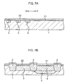
- FIG. 7A and FIG. 7B are schematic cross sectional views, subsequent to FIG. 6A and FIG. 6B , showing the method for manufacturing the semiconductor memory device including the embedded bit line type SONOS transistors in the first embodiment in the order of processes;
- FIG. 8A and FIG. 8B are schematic cross sectional views, subsequent to FIG. 7A and FIG. 7B , showing the method for manufacturing the semiconductor memory device including the embedded bit line type SONOS transistors in the first embodiment in the order of processes;
- FIG. 9A and FIG. 9B are schematic cross sectional views, subsequent to FIG. 8A and FIG. 8B , showing the method for manufacturing the semiconductor memory device including the embedded bit line type SONOS transistors in the first embodiment in the order of processes;
- FIG. 10A and FIG. 10B are schematic cross sectional views, subsequent to FIG. 9A and FIG. 9B , showing the method for manufacturing the semiconductor memory device including the embedded bit line type SONOS transistors in the first embodiment in the order of processes;
- FIG. 11A and FIG. 11B are schematic cross sectional views, subsequent to FIG. 10A and FIG. 10B , showing the method for manufacturing the semiconductor memory device including the embedded bit line type SONOS transistors in the first embodiment in the order of processes;
- FIG. 12A and FIG. 12B are schematic cross sectional views, subsequent to FIG. 11A and FIG. 11B , showing the method for manufacturing the semiconductor memory device including the embedded bit line type SONOS transistors in the first embodiment in the order of processes;
- FIG. 13A and FIG. 13B are schematic cross sectional views, subsequent to FIG. 12A and FIG. 12B , showing the method for manufacturing the semiconductor memory device including the embedded bit line type SONOS transistors in the first embodiment in the order of processes;
- FIG. 14 is a diagrammatic view showing a schematic configuration of a plasma processor provided with a radial line slot antenna used for every embodiment
- FIG. 15A and FIG. 15B are schematic cross sectional views showing a method for manufacturing a semiconductor memory device including floating gate type transistors in a second embodiment in the order of processes;
- FIG. 16A and FIG. 16B are schematic cross sectional views, subsequent to FIG. 15A and FIG. 15B , showing the method for manufacturing the semiconductor memory device including the floating gate type transistors in the second embodiment in the order of processes;
- FIG. 17A and FIG. 17B are schematic cross sectional views, subsequent to FIG. 16A and FIG. 16B , showing the method for manufacturing the semiconductor memory device including the floating gate type transistors in the second embodiment in the order of processes;
- FIG. 18A and FIG. 18B are schematic cross sectional views, subsequent to FIG. 17A and FIG. 17B , showing the method for manufacturing the semiconductor memory device including the floating gate type transistors in the second embodiment in the order of processes;
- FIG. 19A and FIG. 19B are schematic cross sectional views, subsequent to FIG. 18A and FIG. 18B , showing the method for manufacturing the semiconductor memory device including the floating gate type transistors in the second embodiment in the order of processes;
- FIG. 20 is a schematic cross sectional views, subsequent to FIG. 19A and FIG. 19B , showing the method for manufacturing the semiconductor memory device including the floating gate type transistors in the second embodiment in the order of processes;
- FIG. 21A and FIG. 21B are schematic cross sectional views, subsequent to FIG. 20 , showing the method for manufacturing the semiconductor memory device including the floating gate type transistors in the second embodiment in the order of processes;
- FIG. 22A and FIG. 22B are schematic cross sectional views, subsequent to FIG. 21A and FIG. 21B , showing the method for manufacturing the semiconductor memory device including the floating gate type transistors in the second embodiment in the order of processes;
- FIG. 23A and FIG. 23B are schematic cross sectional views, subsequent to FIG. 22A and FIG. 22B , showing the method for manufacturing the semiconductor memory device including the floating gate type transistors in the second embodiment in the order of processes;
- FIG. 24A and FIG. 24B are schematic cross sectional views, subsequent to FIG. 23A and FIG. 23B , showing the method for manufacturing the semiconductor memory device including the floating gate type transistors in the second embodiment in the order of processes;
- FIG. 25A and FIG. 25B are schematic cross sectional views, subsequent to FIG. 24A and FIG. 24B , showing the method for manufacturing the semiconductor memory device including the floating gate type transistors in the second embodiment in the order of processes;
- FIG. 26A and FIG. 26B are schematic cross sectional views, subsequent to FIG. 25A and FIG. 25B , showing the method for manufacturing the semiconductor memory device including the floating gate type transistors in the second embodiment in the order of processes;
- FIG. 27A and FIG. 27B are schematic cross sectional views showing a method for manufacturing a semiconductor memory device including embedded bit line type SONOS transistors in a third embodiment in the order of processes;
- FIG. 28A and FIG. 28B are schematic cross sectional views, subsequent to FIG. 27A and FIG. 27B , showing the method for manufacturing the semiconductor memory device including the embedded bit line type SONOS transistors in the third embodiment in the order of processes;
- FIG. 29A and FIG. 29B are schematic cross sectional views, subsequent to FIG. 28A and FIG. 28B , showing the method for manufacturing the semiconductor memory device including the embedded bit line type SONOS transistors in the third embodiment in the order of processes;
- FIG. 30A and FIG. 30B are schematic cross sectional views, subsequent to FIG. 29A and FIG. 29B , showing the method for manufacturing the semiconductor memory device including the embedded bit line type SONOS transistors in the third embodiment in the order of processes;
- FIG. 31A and FIG. 31B are schematic cross sectional views, subsequent to FIG. 30A and FIG. 30B , showing the method for manufacturing the semiconductor memory device including the embedded bit line type SONOS transistors in the third embodiment in the order of processes;
- FIG. 32A and FIG. 32B are schematic cross sectional views, subsequent to FIG. 31A and FIG. 31B , showing the method for manufacturing the semiconductor memory device including the embedded bit line type SONOS transistors in the third embodiment in the order of processes;
- FIG. 33A and FIG. 33B are schematic cross sectional views, subsequent to FIG. 32A and FIG. 32B , showing the method for manufacturing the semiconductor memory device including the embedded bit line type SONOS transistors in the third embodiment in the order of processes;
- FIG. 34A and FIG. 34B are schematic cross sectional views, subsequent to FIG. 33A and FIG. 33B , showing the method for manufacturing the semiconductor memory device including the embedded bit line type SONOS transistors in the third embodiment in the order of processes;
- FIG. 35A and FIG. 35B are schematic cross sectional views, subsequent to FIG. 34A and FIG. 34B , showing the method for manufacturing the semiconductor memory device including the embedded bit line type SONOS transistors in the third embodiment in the order of processes;
- FIG. 36 is a characteristic chart showing a result of a study in a relationship between a deposition temperature of a silicon nitride film and a threshold value (Vt) shift caused by leaving the silicon nitride film in a high temperature.
- Vt threshold value
- a semiconductor memory device is manufactured under a low temperature condition of 600° C. or below.
- nitriding processing a plasma nitriding method
- a silicon oxide film of a multilayered insulating film is similarly formed by a plasma oxidizing method.
- the plasma nitriding method is a method for conducting nitriding processing in which plasma is excited by microwave in an atmosphere containing a source gas containing a nitride atom in addition to one kind or plural kinds of inert gases among He, Ne, Ar, Kr, Xe, and Rn, for example, one kind selected from NH 3 gas, a mixed gas of N 2 and H 2 , and N 2 gas in addition to the inert gas, or a mixed gas of the NH 3 gas and the N 2 gas, or the NH 3 gas, the mixed gas of N 2 and H 2 so as to generate a nitride radical (N* radical or NH* radical).
- a plasma nitride film of dense and high quality can be obtained in as low temperature as between approximately 200° C. and 600° C.
- Ar and Kr are suitable for the inert gas in which the source gas is contained; the plasma nitride film of best quality can be obtained when Kr is used.
- an oxidizing rate is high when a gas containing hydrogen is used.
- the plasma oxidizing method is a method for conducting oxidizing processing in which plasma is excited by microwave in an atmosphere containing a source gas containing an oxygen atom in addition to one kind or plural kinds of inert gases among He, Ne, Ar, Kr, Xe, and Rn, for example, one kind selected from O 2 , a mixed gas of O 2 and H 2 , and H 2 O gas in addition to the inert gas, or a mixed gas of O 2 and the H 2 O gas, or a mixed gas of O 2 , H 2 , and the H 2 O gas so as to generate an oxide radical (O* radical or OH* radical).
- a plasma oxide film of dense and high quality can be obtained in as low temperature as between approximately 200° C. and 600° C.
- Ar and Kr are suitable for the inert gas in which the source gas is contained; the plasma oxide film of best quality can be obtained when Kr is used.
- an oxidizing rate is high when a gas containing hydrogen is used.
- a multilayered insulating film such as an ON film, an ONO film, or the like is formed on an entire surface including a memory cell region
- the multilayered insulating film in a peripheral circuit region is removed and a gate insulation film is formed in the peripheral circuit region by thermal oxidization.
- the memory cell region is covered with the multilayered insulating film.
- An oxidizing rate of the silicon nitride film is extremely as slow as 1/30 or below compared with that of a surface of a substrate.
- the silicon nitride film does not put through O 2 , and therefore, an upper silicon oxide film of the multilayered insulating film is only slightly increased. The same thing can be said when an oxynitride film is formed as the gate insulation film.
- the multilayered insulating film in a memory cell is not affected very much because the silicon nitride film does not put through N 2 O or NO.
- the silicon nitride film of the multilayered insulating film in the memory cell is oxidized when the silicon oxide film is formed as the gate insulation film, and the silicon oxide film of the multilayered insulating film is further nitrided when a silicon oxynitride film is formed as the gate insulation film.
- a growth rate of the silicon oxide film made by oxidization of the silicon nitride film of the multilayered insulating film is a same as approximately 0.8 times as the growth rate of the silicon oxide film formed by oxidization of a silicon substrate. Therefore, the silicon nitride film is replaced by the silicon oxide film (or the silicon oxide film by the silicon nitride film).
- Inventors of the present invention made up following aspects in consideration to that a peripheral circuit, and especially the gate insulation film therein could be successfully formed by the plasma nitriding method without generating hydrogen and without causing a problem in relation to the multilayered insulating film when the multilayered insulating film of dense and high quality is formed in low temperature, using the plasma nitriding method or the plasma oxidizing method.
- FIG. 1A to FIG. 1C are diagrammatic views for explaining the first aspect.
- an explanation is given with an example that an ONO film is formed in a memory cell region, and that a gate insulation film is formed in a peripheral circuit region.
- a silicon film 103 is formed on the lower silicon oxide film 102 by, for example, a thermal CVD method.
- the polycrystalline silicon film or the a-Si film may be acceptable as the silicon film 103 .
- the a-Si film can grow under a temperature of 575° C. or below, for example, as low as 530° C.
- Silane containing a hydrogen atom is generally used as a raw material gas. However, little hydrogen is generated because the silane does not contain ammonia.
- the silicon film 103 is required to be formed having a film thickness of 5 nm or more in order to prevent from generating “a gap” caused by deposition unevenness.
- the silicon film 103 is completely nitrided by the aforementioned plasma nitriding method to be replaced by a silicon nitride film 104 .
- a preferable processing is possible under a temperature condition of as low as 530° C. or below, for example, 400° C.
- the low temperature treatment prevents hydrogen in the silicon nitride film from desorbing and diffusing to the lower silicon oxide film.
- plasma processing can be conducted without using hydrogen as a raw material gas.
- a surface layer of the silicon nitride film 104 is completely oxidized by the aforementioned plasma oxidizing method to be replaced by an upper silicon oxide film 105 .
- An ONO film 111 as a multilayered insulating film composed of the lower silicon oxide film 102 , the silicon nitride film 104 , and the upper silicon oxide film 105 is formed.
- a preferable processing is possible under a temperature condition of as low as 530° C. or below, for example, 400° C. when the upper silicon oxide film 105 is formed.
- plasma processing can be conducted without using hydrogen as a raw material gas.
- a gate insulation film 112 may be preferably formed in a peripheral circuit region of a semiconductor substrate simultaneously with the upper silicon oxide film 105 .
- the gate insulation film 112 is simultaneously formed by plasma oxidization for forming the upper silicon oxide film 105 while the ONO film 111 is formed (in a state that the lower silicon oxide film 102 and the silicon nitride film 104 are formed). Therefore, strong oxidizing power due to plasma oxidization does not have to be concerned.
- a total film thickness of the lower silicon oxide film 102 and the silicon nitride film 104 is preferably approximately 15 nm or more.
- FIG. 2A and FIG. 2B are diagrammatic views for explaining the second aspect.
- an explanation is also given with an example that an ONO film is formed in a memory cell region, and that a gate insulation film is formed in a peripheral circuit region.
- a surface layer of a silicon region 201 which is a memory cell region of a silicon semiconductor substrate, or is a polycrystalline silicon film or an a-Si film (for example, an island-shaped floating gate) formed in the memory cell region, is completely nitrided to form a silicon nitride film 202 by the aforementioned plasma nitriding method.
- a preferable processing is possible under a temperature condition of as low as 530° C. or below, for example, 400° C.
- the low temperature treatment prevents hydrogen in the silicon nitride film from desorbing and diffusing to the lower silicon oxide film.
- plasma processing can be conducted without using hydrogen as a raw material gas.
- a surface layer of the silicon nitride film 202 is oxidized by the aforementioned plasma oxidizing method.
- the silicon nitride film 202 is formed to have a film thickness of 15 nm or below by the aforementioned plasma nitriding so as to oxidize not only the surface layer of the silicon nitride film 202 but also an interface of the silicon region 201 facing with the silicon nitride film 202 . Therefore, an ONO film 211 as a multilayered insulating film composed of the lower silicon oxide film 203 , the silicon nitride film 202 , and the upper silicon oxide film 204 is formed.
- a preferable processing is possible under a temperature condition of as low as 530° C. or below, for example, 400° C. when the lower silicon oxide film 203 and the upper silicon oxide film 204 are formed. Furthermore, by generating only the O* radical as a radical, plasma processing can be conducted without using hydrogen as a raw material gas.
- a gate insulation film 212 may be formed in a peripheral circuit region of a semiconductor substrate simultaneously with the lower silicon oxide film 203 and the upper silicon oxide film 204 .
- the gate insulation film 212 is simultaneously formed by plasma oxidization for forming the lower silicon oxide film 203 and the upper silicon oxide film 204 while the ONO film 211 is formed (in a state that the silicon nitride film 202 is formed). Therefore, strong oxidizing power due to the plasma oxidization can be utilized.
- FIG. 3A and FIG. 3B are diagrammatic views for explaining the third aspect.
- an explanation is also given with an example that an ONO film is formed in a memory cell region, and that a gate insulation film is formed in a peripheral circuit region.
- a silicon nitride film 303 is formed on the lower silicon oxide film 302 by, for example, a thermal CVD method or a plasma CVD method.
- the silicon nitride film formed by the CVD method contains many lattice defects, and therefore, it is suitable when used as a charge-storage film.
- a surface layer of the silicon nitride film 303 is oxidized by the aforementioned plasma oxidizing method to be replaced by an upper silicon oxide film 304 .
- An ONO film 311 as a multilayered insulating film composed of the lower silicon oxide film 302 , the silicon nitride film 303 , and the upper silicon oxide film 304 is formed.
- a preferable processing is possible under a temperature condition of as low as 530° C. or below, for example, 400° C. when the upper silicon oxide film 304 is formed.
- plasma processing can be conducted without using hydrogen as a raw material gas.
- a gate insulation film 312 may be formed in a peripheral circuit region of a semiconductor substrate simultaneously with the upper silicon oxide film 304 .
- the gate insulation film 312 is simultaneously formed by plasma oxidization for forming the upper silicon oxide film 304 while the ONO film 311 is formed (in a state that the lower silicon oxide film 302 and the silicon nitride film 303 are formed). Therefore, strong oxidizing power due to the plasma oxidization can be utilized.
- a semiconductor memory device having an embedded bit line type SONOS structure will be disclosed.
- a structure of the semiconductor memory device is explained with a method for manufacturing thereof as a matter of convenience.
- This semiconductor memory device is so structured that SONOS transistors in a memory cell region are of a planer type and that CMOS transistors are formed in a peripheral circuit region.
- FIG. 4A to FIG. 13B are schematic cross sectional views showing a method for manufacturing the semiconductor memory device including embedded bit line type SONOS transistors in this embodiment in the order of processes.
- each A of the drawings shows a memory cell region (a core region), and each B thereof shows a peripheral circuit region.
- the left side of the A thereof corresponds to a cross section (an X section) taken along the parallel line to a gate electrode (a word line), and the right side corresponds to a cross section (a Y section) taken along the perpendicular line to the gate electrode.
- element isolation structures are formed in a peripheral circuit region 12 to demarcate element active regions.
- STI Shallow Trench Isolation
- wells 3 , 4 , and 5 are formed in the peripheral circuit region 12 .
- n-type impurities such as phosphorus (P), arsenic (As), or the like are ion-implanted into only an n-type region of the peripheral circuit region 12 , and the impurities are thermally diffused by annealing treatment to form the n-well 3 in the n-type region.
- the n-type impurities such as phosphorus (P), arsenic (As), or the like are deeply ion-implanted into only a p-type region of the peripheral circuit region 12 , and a p-type impurity such as boron (B) is less shallowly ion-implanted than the n-type impurities.
- the impurities are thermally diffused by annealing treatment to form the deep n-well 4 and the p-well 5 in the n-well 4 so as to form a triple-well structure in the p-type region.
- bit-line diffusion layers 6 are formed in a core region 11 of the semiconductor substrate 1 .
- bit-line diffusion layers 6 are formed by lithography, and using them as masks, an n-type impurity, arsenic (As) in this example, is ion-implanted.
- As arsenic
- it is ion-implanted with a dose amount of 2.0 ⁇ 10 14 (/cm 2 ) or more in order to lower bit-line resistance.
- the bit-line diffusion layers 6 also serving as sources/drains are formed.
- a resist mask (not shown) covering only the p-type region of the peripheral circuit region 12 is formed. Furthermore, using this as a mask, ion-implantation of boron (B) for threshold value adjustment is conducted (shown as a reference numeral 41 ). Incidentally, this ion-implantation is not limited to the p-type region, and is applicable to the n-type region.
- a plasma oxidizing method and a plasma nitriding method through microwave excitation are used for forming the ONO film.
- a plasma processor as shown in FIG. 14 , provided with a radial line slot antenna, is used for plasma oxidizing and plasma nitriding.
- This plasma processor 1000 includes a gate valve 1002 communicating with a cluster tool 1001 , a process chamber 1005 capable of accommodating a susceptor on which an object to be processed (the semiconductor substrate 1 in this embodiment) is to be mounted and which is provided with a cooling jacket 1003 for cooling the object to be processed at the time of plasma processing, a high-vacuum pump 1006 connected to the process chamber 1005 , a microwave supply source 1010 , an antenna member 1020 , a bias high-frequency power source 1007 and a matching box 1008 constituting an ion plating apparatus together with this antenna member 1020 , gas supply systems 1030 , 1040 having gas supply rings 1031 , 1041 , and a temperature control section 1050 for controlling the temperature of the object to be processed.
- the microwave supply source 1010 is made from, for example, magnetron and is generally capable of generating a microwave (for example, 5 kW) of 2.45 GHz.
- the transmission mode of the microwave is thereafter converted to a TM, TE, TEM mode or the like by a mode converter 1012 .
- the antenna member 1020 has a temperature-adjusting plate 1022 , an accommodating member 1023 , and a dielectric plate.
- the temperature-adjusting plate 1022 is connected to a temperature control unit 1021 , and the accommodating member 1023 accommodates a wavelength shortening material 1024 and a slot electrode (not shown) being in contact with the wavelength shortening material 1024 .
- This slot electrode is called a radial line slot antenna (RLSA) or an ultra-high efficiency flat antenna.
- RLSA radial line slot antenna
- a different type of antenna for example, a single-layer waveguide flat antenna, a dielectric substrate parallel plane slot array, or the like may be applied.
- lower silicon oxide films 21 are firstly formed on silicon surfaces of the element active regions by a plasma oxidizing method.
- oxidizing processing is conducted by generating an oxygen radical (O*) by irradiating the source gas with a microwave of 3.5 kW under a temperature condition of 450° C. so as to form the lower silicon oxide films 21 .
- O* oxygen radical
- the lower silicon oxide films might be formed by a thermal oxidation method or a CVD oxide method instead of the plasma oxidizing.
- amorphous silicon (a-Si) films 31 are deposited to have a film thickness of approximately 9 nm on the lower silicon oxide films 21 by a thermal CVD method under a temperature condition of 530° C., using SiH 4 as a raw material gas.
- a-Si amorphous silicon
- polycrystalline silicon films may be formed instead of the a-Si films.
- the a-Si films 31 are completely nitrided by a plasma nitriding method to form silicon nitride films 22 on the lower silicon oxide films 21 .
- nitriding processing is conducted by generating a nitrogen radical (N*) by irradiating the source gas with a microwave of 3.5 kW under a temperature condition of 450° C.
- N* nitrogen radical
- the a-Si films 31 having a film thickness of approximately 9 nm are completely nitrided to be replaced by the silicon nitride films 22 having a film thickness of approximately 18 nm.
- surface layers of the silicon nitride films 22 are oxidized by a plasma oxidizing method to form upper silicon oxide films.
- a plasma oxidizing method to form upper silicon oxide films.
- gate insulation films are respectively formed in the peripheral circuit region 12 with the upper silicon oxide film in the core region 11 .
- the silicon nitride film 22 formed in the peripheral circuit region 12 is removed by dry etching.
- the lower silicon oxide film 21 formed in the peripheral circuit region 12 is removed by HF treatment so as to expose the surface of the semiconductor substrate 1 in the peripheral circuit region 12 .
- oxidizing processing is conducted by generating an oxygen radical (O*) by irradiating the source gas with a microwave of 3.5 kW under a temperature condition of 450° C.
- a silicon oxide film 30 is formed by oxidizing a surface layer of the silicon nitride film 22 in the core region 11 .
- a silicon oxide film 32 having a film thickness of approximately 8 nm is formed in the peripheral circuit region 12 .
- a part for forming a thin gate insulation film in the peripheral circuit region 12 that is, a resist mask (not shown) for exposing only the n-type region, is formed.
- HF treatment is conducted using it as a mask, thereby removing the silicon oxide film 32 in the n-type region.
- oxidizing processing is conducted by the aforementioned plasma oxidizing method so as to form a silicon oxide film having a film thickness of approximately 7 nm on a surface of the exposed semiconductor substrate 1 .
- the surface layer of the silicon nitride film 22 is further oxidized and replaced by a silicon oxide film, and as a result, an upper silicon oxide film 23 having a film thickness of approximately 10 nm is formed.
- a thin gate insulation film 24 having a film thickness of approximately 7 nm is formed in the n-type region.
- a gate insulation film 25 having a film thickness of approximately 13 nm is formed in the p-type region by plasma oxidization having a film thickness of approximately 7 nm after plasma oxidization having a film thickness of aforementioned 8 nm (the silicon oxide film 32 ).
- an ONO film 7 is thus composed of the lower silicon oxide film 21 having a film thickness of approximately 8 nm formed by plasma oxidization, the silicon nitride film 22 having a film thickness of approximately 8 nm formed by plasma nitriding as a charge-storage film whose surface layer is reduced by plasma oxidization twice, and the upper silicon oxide film 23 formed by plasma oxidization.
- a thin gate insulation film 24 having a film thickness of approximately 8 nm in the n-type region and a gate insulation film 25 having a film thickness of approximately 13 nm in the p-type region are respectively formed.
- polycrystalline silicon films 33 are formed on entire surfaces of the core region 11 and the peripheral circuit region 12 by a CVD method.
- the polycrystalline silicon films 33 are patterned by lithography followed by dry etching to form gate electrodes 8 in the core region 11 , and the n-type region and the p-type region of the peripheral circuit region 12 , respectively. At this time, these gate electrodes 8 in the core region 11 are formed to cross the bit line diffusion layers 6 substantially perpendicularly.
- sources/drains 9 and 10 are formed only in the peripheral circuit region 12 .
- n-type impurities are ion-implanted into the surface of the semiconductor substrate 1 on both sides of the gate electrode 8 in the n-type region to form extension regions 26 .
- p-type impurities are ion-implanted into the surface of the semiconductor substrate 1 on both sides of the gate electrode 8 to form extension regions 27 .
- the entire surface of the silicon oxide film is antisotropically etched (etch back) so as to leave only the silicon oxide films on both sides of the respective gate electrodes 8 , thereby forming sidewalls 28 .
- n-type impurities are ion-implanted into the surface of the semiconductor substrate 1 on both sides of the gate electrodes 8 and the sidewalls 28 to form the deep sources/drains 9 which partly overlap the extension regions 26 .
- p-type impurities are ion-implanted into the surface of the semiconductor substrate 1 on both sides of the gate electrode 8 and the sidewalls 28 to form the deep sources/drains 10 which partly overlap the extension regions 27 .
- surfaces of the sources/drains 9 and 10 may be exposed so as to form siliside layers on the sources/drains 9 and 10 , and on the gate electrodes 8 in the peripheral circuit region 12 by conducting salicide process.
- a several-layered interlayer dielectric covering the entire surface, contact holes, via holes, various kinds of wiring layers, and so on are formed, and a protective insulation film (none of them are shown) is formed on a top layer so that, on the semiconductor substrate 1 , many semiconductor memory devices provided with a peripheral circuit including SONOS type memory cells and the CMOS transistors are formed. Then, an individual semiconductor memory device is manufactured by separating and packaging the above-mentioned devices.
- the ONO film 7 functioning as a charge-storage film is formed of high quality and in low temperature, and furthermore, the gate insulation films 24 and 25 in the peripheral circuit are successfully formed with the ONO film 7 .
- a floating gate type semiconductor memory device will be disclosed.
- a structure of the semiconductor memory device is explained with a method for manufacturing thereof as a matter of convenience.
- the floating gate type transistors are formed in a memory cell region, and CMOS transistors are formed in a peripheral circuit region.
- FIG. 15A to FIG. 26B are schematic cross sectional views showing a method for manufacturing the semiconductor memory device including the floating gate type transistors in this embodiment in the order of processes.
- each A of the drawings except FIG. 20 shows a memory cell region (a core region), and each B thereof shows a peripheral circuit region.
- the left side of the A thereof corresponds to a cross section (an X section) taken along the parallel line to a control gate (a word line), and the right side corresponds to a cross section (a Y section) taken along the perpendicular line to the control gate.
- FIG. 20 corresponds to the X section.
- element isolation structures are respectively formed in a core region 11 and a peripheral circuit region 12 to demarcate element active regions.
- STI Shallow Trench Isolation
- wells 3 , 4 , and 5 are formed in the peripheral circuit region 12 .
- n-type impurities such as phosphorus (P), arsenic (As), or the like are ion-implanted into only an n-type region of the peripheral circuit region 12 , and the impurities are thermally diffused by annealing treatment to form the n-well 3 in the n-type region.
- the n-type impurities such as phosphorus (P), arsenic (As), or the like are deeply ion-implanted into only a p-type region of the peripheral circuit region 12 , and a p-type impurity such as boron (B) is less shallowly ion-implanted than the n-type impurities.
- the impurities are thermally diffused by annealing treatment to form the deep n-well 4 and the p-well 5 in the n-well 4 so as to form a triple-well structure in the p-type region.
- a resist mask (not shown) covering only the p-type region of the peripheral circuit region 12 is formed. Furthermore, using this as a mask, ion-implantation of boron (B) for threshold value adjustment is conducted (shown as a reference numeral 41 ). Incidentally, this ion-implantation is not limited to the p-type region, and is applicable to the n-type region.
- tunnel oxide films 42 having a film thickness of approximately 10 nm are formed in the respective element active regions by thermal oxidation.
- the aforementioned plasma oxidizing method is also suitable for forming the tunnel oxide films instead of a thermal oxidation method.
- amorphous silicon (a-Si) films 43 formed by doping phosphorus (P) are entirely deposited to have a film thickness of approximately 90 nm by a thermal CVD method under a temperature condition of 530° C., using SiH 4 and PH 3 as raw material gases.
- the a-Si film 43 is patterned by lithography followed by dry etching to form floating gates 44 which are individually divided perpendicular to later-described word lines.
- the a-Si film 43 is entirely left.
- an ONO film which is a multilayered insulating film is formed as a dielectric film.
- silicon nitride films 45 are formed by the aforementioned plasma nitriding method.
- nitriding processing of surface layers of the a-Si films 43 is conducted by generating a nitrogen radical (N*) by irradiating the source gas with a microwave of 3.5 kW under a temperature condition of 450° C. so as to form the silicon nitride films 45 having a film thickness of approximately 12 nm.
- N* nitrogen radical
- a lower silicon oxide film 46 and an upper silicon oxide film 47 are simultaneously formed above and below the silicon nitride film 45 by the aforementioned plasma oxidizing method.
- oxidizing processing is conducted by generating an oxygen radical (O*) by irradiating the source gas with a microwave of 3.5 kW under a temperature condition of 450° C.
- the lower silicon oxide film 46 is formed by replacing an interface of the a-Si film 43 which is approximately 4 nm in thickness facing with the silicon nitride film 45 by an oxide film.
- the upper silicon oxide film 47 is formed by replacing an upper layer of approximately 5 nm in thickness of the silicon nitride film 45 by an oxide film.
- an ONO film 51 composed of the lower silicon oxide film 46 having a film thickness of approximately 4 nm on the floating gate 44 whose film thickness is reduced to approximately 81 nm by the aforementioned plasma nitriding and plasma oxidization, the silicon nitride film 45 whose film thickness is reduced to approximately 6 nm, and the upper silicon oxide film 47 having a film thickness of approximately 4 nm is formed.
- the three layers 45 , 46 , and 47 are shown as a single-layered ONO film 51 for simplification from the following FIG. 21A to FIG. 26B as a matter of convenience.
- the ONO film 51 and the a-Si film 43 in the peripheral circuit region 12 are removed by dry etching. Furthermore, the silicon surface of the element active regions in the peripheral circuit region 12 is exposed by HF treatment.
- the silicon surface of the element active regions in the peripheral circuit region 12 is thermally oxidized to form silicon oxide films 48 having a film thickness of approximately 8 nm.
- oxidizing power by thermal oxidation method is not so strong that oxidation of the ONO film 51 in the core region 11 can be ignored.
- the silicon oxide film 48 in the n-type region is removed by HF treatment.
- thermal oxidization is conducted so as to form a silicon oxide film having a film thickness of approximately 7 nm on the silicon surfaces in the n-type and the p-type region in the peripheral circuit region 12 .
- a thin gate insulation film 49 having a film thickness of approximately 10 nm is formed in the n-type region.
- a gate insulation film 50 having a film thickness of 16 nm is formed in the p-type region as a result of thermal oxidation having a film thickness of approximately 10 nm after thermal oxidation having a film thickness of aforementioned 8 nm.
- a-Si films 52 are deposited on entire surfaces by a CVD method, as shown in FIG. 26A and 26B , the a-Si films 52 (and the a-Si film 43 in the core region 11 ) are patterned by lithography followed by dry etching.
- control gates 53 functioning as word lines for conducting capacity coupling with the floating gates 44 through the ONO film 51 as the dielectric film are formed.
- gate electrodes 54 as components of the CMOS transistors are formed.
- protruding parts of the control gates 53 from the floating gates 44 are removed simultaneously when the control gates 53 are formed.
- extension regions 81 are formed only in the core region 11 .
- n-type impurities are ion-implanted into the surface of the semiconductor substrate 1 on both sides of the control gates 53 to form the extension regions 81 .
- extension regions 26 and 27 are formed only in the peripheral circuit region 12 .
- n-type impurities are ion-implanted into the surface of the semiconductor substrate 1 on both sides of the gate electrode 54 in the n-type region to form the extension regions 26 .
- p-type impurities are ion-implanted into the surface of the semiconductor substrate 1 on both sides of the gate electrode 54 to form the extension regions 27 .
- the entire surface of the silicon oxide film is antisotropically etched (etch back) so as to leave only the silicon oxide films on both sides of the respective gate electrodes 54 , thereby forming sidewalls 28 .
- n-type impurities are ion-implanted into the surface of the semiconductor substrate 1 on both sides of the control gates 53 and the sidewalls 28 to form sources/drains 82 which partly overlap the extension regions 81 .
- n-type impurities are ion-implanted into the surface of the semiconductor substrate 1 on both sides of the gate electrodes 54 and the sidewalls 28 to form deep sources/drains 9 which partly overlap the extension regions 26 .
- p-type impurities are ion-implanted into the surface of the semiconductor substrate 1 on both sides of the gate electrode 54 and the sidewalls 28 to form deep sources/drains 10 which partly overlap the extension regions 27 .
- surfaces of the sources/drains 9 and 10 may be exposed so as to form siliside layers on the sources/drains 9 and 10 , and on the gate electrodes 54 in the peripheral circuit region 12 by conducting salicide process.
- a several-layered interlayer dielectric covering the entire surface, contact holes, via holes, various kinds of wiring layers, and so on are formed, and a protective insulation film (none of them are shown) is formed on a top layer so that, on the semiconductor substrate 1 , many semiconductor memory devices provided with a peripheral circuit including floating gate type memory cells and the CMOS transistors are formed. Then, an individual semiconductor memory device is manufactured by separating and packaging the above-mentioned devices.
- the ONO film 51 functioning as the dielectric film is formed in low temperature and of high quality, and, the silicon oxide films above and below the silicon nitride film are simultaneously formed. This decreases the number of processes and makes it possible to realize a floating gate type semiconductor memory device of high reliability and low cost.
- a semiconductor memory device having an embedded bit line type SONOS structure will be disclosed.
- a structure of the semiconductor memory device is explained with a method for manufacturing thereof as a matter of convenience.
- This semiconductor memory device is so structured that SONOS transistors in a memory cell region are of a planer type and that CMOS transistors are formed in a peripheral circuit region.
- FIG. 27A to FIG. 35B are schematic cross sectional views showing a method for manufacturing the semiconductor memory device including embedded bit line type SONOS transistors in this embodiment in the order of processes.
- each A of the drawings shows a memory cell region (a core region), and each B thereof shows a peripheral circuit region.
- the left side of the A thereof corresponds to a cross section (an X section) taken along the parallel line to a gate electrode (a word line), and the right side corresponds to a cross section (a Y section) taken along the perpendicular line to the gate electrode.
- wells 3 , 4 , and 5 are formed in a peripheral circuit region 12 .
- n-type impurities such as phosphorus (P), arsenic (As), or the like are ion-implanted into only an n-type region of the peripheral circuit region 12 , and the impurities are thermally diffused by annealing treatment to form the n-well 3 in the n-type region.
- the n-type impurities such as phosphorus (P), arsenic (As), or the like are deeply ion-implanted into only a p-type region of the peripheral circuit region 12 , and a p-type impurity such as boron (B) is less shallowly ion-implanted than the n-type impurities.
- the impurities are thermally diffused by annealing treatment to form the deep n-well 4 and the p-well 5 in the n-well 4 so as to form a triple-well structure in the p-type region.
- element isolation structures are formed in a peripheral circuit region 12 to demarcate element active regions.
- field oxide films 61 are formed in element isolation regions in the peripheral circuit region 12 of a p-type silicon semiconductor substrate 1 so as to demarcate the element active regions.
- element isolation structures are not formed in the core region.
- a resist mask (not shown) covering only the p-type region of the peripheral circuit region 12 is formed. Furthermore, using this as a mask, ion-implantation of boron (B) for threshold value adjustment is conducted (shown as a reference numeral 41 ). Incidentally, this ion-implantation is not limited to the p-type region, and is applicable to the n-type region.
- bit-line diffusion layers 6 are formed in a core region 11 of the semiconductor substrate 1 .
- bit-line diffusion layers 6 are formed by lithography, and using them as masks, an n-type impurity, arsenic (As) in this example, is ion-implanted.
- As arsenic
- it is ion-implanted with a dose amount of 2.0 ⁇ 10 14 (/cm 2 ) or more in order to lower bit-line resistance.
- the bit-line diffusion layers 6 also serving as sources/drains are formed.
- lower silicon oxide films 62 are formed on silicon surfaces of the element active regions by the aforementioned plasma oxidizing method.
- oxidizing processing is conducted by generating an oxygen radical (O*) by irradiating the source gas with a microwave of 3.5 kW under a temperature condition of 450° C. so as to form the lower silicon oxide films 62 .
- O* oxygen radical
- the lower silicon oxide films 62 are formed, by using the plasma oxidization instead of a thermal oxidization, dense films are formed in low temperature, thereby controlling impurity diffusion of the bit-line diffusion layers 6 .
- silicon nitride films 63 are formed on the lower silicon oxide films 62 by a thermal CVD method.
- the silicon nitride films 63 are deposited to have a film thickness of approximately 15 nm by the thermal CVD method under a temperature condition of 730° C., using SiH 2 Cl 2 and NH 3 as raw material gases.
- the silicon nitride films functioning as charge-storage films with many traps suitable for SONOS type memory cells can be formed.
- FIG. 30A and FIG. 30B only the core region 11 is covered with a resist mask (not shown), and using it as a mask, the silicon nitride film 63 formed in the peripheral circuit region 12 is removed by dry etching. Subsequently, the lower silicon oxide film 62 .formed in the peripheral circuit region 12 is removed by HF treatment so as to expose the surface of the semiconductor substrate 1 in the peripheral circuit region 12 .
- an upper silicon oxide film 64 in the core region 11 , and gate insulation films 24 and 25 in the peripheral circuit region 12 are formed by plasma oxidizing method.
- oxidizing processing is conducted by generating an oxygen radical (O*) by irradiating the source gas with a microwave of 3.5 kW under a temperature condition of 450° C.
- a silicon oxide film 70 is formed by oxidizing a surface layer of the silicon nitride film 63 in the core region 11 .
- a silicon oxide film 32 having a film thickness of approximately 8 nm is formed in the peripheral circuit region 12 .
- a part for forming a thin gate insulation film in the peripheral circuit region 12 that is, a resist mask (not shown) for exposing only the n-type region is formed.
- HF treatment is conducted using it as a mask, thereby removing the silicon oxide film 32 in the n-type region.
- oxidizing processing is conducted by the aforementioned plasma oxidizing method so as to form a silicon oxide film having a film thickness of approximately 7 nm on a surface of the exposed semiconductor substrate 1 .
- the surface layer of the silicon nitride film 63 is further oxidized and replaced by a silicon oxide film, and as a result, an upper silicon oxide film 64 having a film thickness of approximately 10 nm is formed.
- a thin gate insulation film 24 having a film thickness of approximately 7 nm is formed in the n-type region.
- a gate insulation film 25 having a film thickness of approximately 13 nm is formed as a result of plasma oxidization having a film thickness of approximately 7 nm after plasma oxidization having a film thickness of aforementioned 8 nm (the silicon oxide film 32 ) in the p-type region.
- an ONO film 71 composed of the lower silicon oxide film 62 having a film thickness of approximately 8 nm formed by plasma oxidization, the silicon nitride film 63 having a film thickness of approximately 10 nm formed by thermal CVD as a charge-storage film whose surface layer is reduced by plasma oxidization twice, and the upper silicon oxide film 64 formed by plasma oxidization is formed.
- a thin gate insulation film 24 having a film thickness of approximately 8 nm in the n-type region and a gate insulation film 25 having a film thickness of approximately 13 nm in the p-type region are respectively formed.
- polycrystalline silicon films 33 are firstly formed and tungsten silicide films 72 are secondly formed by a CVD method.
- the polycrystalline silicon films 33 and the tungsten silicide film 72 are patterned by lithography followed by dry etching to form gate electrodes 73 in the core region 11 , and the n-type region and the p-type region of the peripheral circuit region 12 , respectively.
- these gate electrodes 73 in the core region 11 are formed to cross the bit line diffusion layers 6 substantially perpendicularly.
- sources/drains 9 and 10 are formed only in the peripheral circuit region 12 .
- n-type impurities are ion-implanted into the surface of the semiconductor substrate 1 on both sides of the gate electrode 73 in the n-type region to form extension regions 26 .
- p-type impurities are ion-implanted into the surface of the semiconductor substrate 1 on both sides of the gate electrode 73 to form extension regions 27 .
- the entire surface of the silicon oxide film is antisotropically etched (etch back) so as to leave only the silicon oxide films on both sides of the respective gate electrodes 73 , thereby forming sidewalls 28 .
- n-type impurities are ion-implanted into the surface of the semiconductor substrate 1 on both sides of the gate electrode 73 and the sidewalls 28 to form the deep sources/drains 9 which partly overlap the extension regions 26 .
- p-type impurities are ion-implanted into the surface of the semiconductor substrate 1 on both sides of the gate electrode 73 and the sidewalls 28 to form the deep sources/drains 10 which partly overlap the extension regions 27 .
- a several-layered interlayer dielectric covering the entire surface, contact holes, via holes, various kinds of wiring layers, and so on are formed, and a protective insulation film (none of them are shown) is formed on a top layer so that, on the semiconductor substrate 1 , many semiconductor memory devices provided with a peripheral circuit including the SONOS type memory cells and the CMOS transistors are formed. Then, an individual semiconductor memory device is manufactured by separating and packaging the above-mentioned devices.
- the ONO film 71 functioning as a charge-storage film is formed of high quality while maintaining a high charge-storage function, and furthermore, the gate insulation films 24 and 25 in the peripheral circuit are successfully formed with the ONO film 71 .
- the present invention is not limited to the aforementioned embodiments.
- the ONO film is explained as the multilayered insulating film; however, the embodiments are also suitable for an ON film composed of the silicon nitride film on the silicon oxide film.
- a silicon film is deposited, and the silicon film is completely nitrided to form the silicon nitride film by the aforementioned plasma nitriding method.
- the surface layer of the silicon oxide film is completely nitrided to form the silicon nitride film by the aforementioned plasma nitriding method after the silicon oxide film is formed by a CVD method, or the like.
- a multilayered insulating film such as an ON film, an ONO film, or the like is formed of high quality and in low temperature without generating hydrogen, capable of realizing a semiconductor memory device of high reliability.
Abstract
Description
Claims (12)
Priority Applications (1)
| Application Number | Priority Date | Filing Date | Title |
|---|---|---|---|
| US11/441,237 US20060228899A1 (en) | 2002-08-30 | 2006-05-26 | Semiconductor memory device and method for manufacturing semiconductor device |
Applications Claiming Priority (2)
| Application Number | Priority Date | Filing Date | Title |
|---|---|---|---|
| JP2002256195A JP2004095918A (en) | 2002-08-30 | 2002-08-30 | Semiconductor memory device and its manufacturing method |
| JP2002-256195 | 2002-08-30 |
Related Child Applications (1)
| Application Number | Title | Priority Date | Filing Date |
|---|---|---|---|
| US11/441,237 Division US20060228899A1 (en) | 2002-08-30 | 2006-05-26 | Semiconductor memory device and method for manufacturing semiconductor device |
Publications (2)
| Publication Number | Publication Date |
|---|---|
| US20040043638A1 US20040043638A1 (en) | 2004-03-04 |
| US7098147B2 true US7098147B2 (en) | 2006-08-29 |
Family
ID=31492692
Family Applications (2)
| Application Number | Title | Priority Date | Filing Date |
|---|---|---|---|
| US10/643,967 Expired - Fee Related US7098147B2 (en) | 2002-08-30 | 2003-08-20 | Semiconductor memory device and method for manufacturing semiconductor device |
| US11/441,237 Abandoned US20060228899A1 (en) | 2002-08-30 | 2006-05-26 | Semiconductor memory device and method for manufacturing semiconductor device |
Family Applications After (1)
| Application Number | Title | Priority Date | Filing Date |
|---|---|---|---|
| US11/441,237 Abandoned US20060228899A1 (en) | 2002-08-30 | 2006-05-26 | Semiconductor memory device and method for manufacturing semiconductor device |
Country Status (6)
| Country | Link |
|---|---|
| US (2) | US7098147B2 (en) |
| EP (1) | EP1394853A3 (en) |
| JP (1) | JP2004095918A (en) |
| KR (1) | KR101018371B1 (en) |
| CN (1) | CN1485891A (en) |
| TW (1) | TWI264113B (en) |
Cited By (19)
| Publication number | Priority date | Publication date | Assignee | Title |
|---|---|---|---|---|
| US20060246661A1 (en) * | 2005-04-08 | 2006-11-02 | Samsung Electronics Co., Ltd. | Method of forming a thin layer and method of manufacturing a non-volatile semiconductor device using the same |
| US20060246633A1 (en) * | 2005-04-28 | 2006-11-02 | Semiconductor Energy Laboratory Co., Ltd. | Manufacturing method of thin film transistor, display device using thin film transistor, and electronic device incorporating display device |
| US20070093013A1 (en) * | 2005-10-20 | 2007-04-26 | Chua Thai C | Method for fabricating a gate dielectric of a field effect transistor |
| US20070093012A1 (en) * | 2005-10-20 | 2007-04-26 | Applied Materials, Inc. | Method for fabricating a gate dielectric of a field effect transistor |
| US20070117353A1 (en) * | 2003-11-25 | 2007-05-24 | Macronix International Co., Ltd. | Method for Forming Oxide on Ono Structure |
| US20070221294A1 (en) * | 2006-03-27 | 2007-09-27 | Tokyo Electron Limited | Plasma processing apparatus and plasma processing method |
| US20070228453A1 (en) * | 2006-03-31 | 2007-10-04 | Shunpei Yamazaki | Nonvolatile semiconductor memory device |
| US20070235794A1 (en) * | 2006-03-21 | 2007-10-11 | Semiconductor Energy Laboratory Co., Ltd. | Nonvolatile semiconductor memory device |
| US20070235793A1 (en) * | 2006-03-21 | 2007-10-11 | Semiconductor Energy Laboratory Co., Ltd. | Nonvolatile semiconductor memory device |
| US20080132083A1 (en) * | 2006-11-30 | 2008-06-05 | Tokyo Electron Limited | Film formation apparatus for semiconductor process and method for using the same |
| US20100041193A1 (en) * | 2004-06-23 | 2010-02-18 | Kabushiki Kaisha Toshiba | Nonvolatile semiconductor memory device and method of manufacturing the same |
| US20100159661A1 (en) * | 2006-02-10 | 2010-06-24 | Semiconductor Energy Laboratory Co., Ltd. | Nonvolatile semiconductor storage device and manufacturing method thereof |
| US20110031501A1 (en) * | 2005-08-12 | 2011-02-10 | Semiconductor Energy Laboratory Co., Ltd. | Display device and manufacturing method of display device |
| US20110217844A1 (en) * | 2010-03-02 | 2011-09-08 | Renesas Electronics Corporation | Method of manufacturing semiconductor device |
| US20110220983A1 (en) * | 2006-03-31 | 2011-09-15 | Semiconductor Energy Laboratory Co., Ltd. | Method for deleting data from nand type nonvolatile memory |
| US8222111B1 (en) | 2006-12-22 | 2012-07-17 | Cypress Semiconductor Corporation | Simultaneous formation of a top oxide layer in a silicon-oxide-nitride-oxide-silicon (SONOS) transistor and a gate oxide in a metal oxide semiconductor (MOS) |
| US20120276730A1 (en) * | 2011-04-27 | 2012-11-01 | Nanya Technology Corporation | Methods for fabricating a gate dielectric layer and for fabricating a gate structure |
| US9132693B2 (en) | 2008-09-16 | 2015-09-15 | Koninklijke Philps N.V. | Capacitive micromachine ultrasound transducer |
| US20170018430A1 (en) * | 2015-07-16 | 2017-01-19 | Silergy Semiconductor Technology (Hangzhou) Ltd | Semiconductor structure and manufacture method thereof |
Families Citing this family (63)
| Publication number | Priority date | Publication date | Assignee | Title |
|---|---|---|---|---|
| TWI229368B (en) * | 2003-02-13 | 2005-03-11 | Tokyo Electron Ltd | Manufacturing method for semiconductor device and semiconductor manufacturing device |
| KR100559994B1 (en) * | 2003-08-08 | 2006-03-13 | 동부아남반도체 주식회사 | Method for forming floating gate of flash memory using sidewall process |
| US6992370B1 (en) * | 2003-09-04 | 2006-01-31 | Advanced Micro Devices, Inc. | Memory cell structure having nitride layer with reduced charge loss and method for fabricating same |
| JP4522916B2 (en) * | 2005-06-27 | 2010-08-11 | 東京エレクトロン株式会社 | Plasma nitriding method, control program, computer storage medium, and plasma processing apparatus |
| KR100539158B1 (en) * | 2004-04-20 | 2005-12-26 | 주식회사 하이닉스반도체 | Method for forming dielectric layer of inter gates of flash memory device |
| JP4477422B2 (en) | 2004-06-07 | 2010-06-09 | 株式会社ルネサステクノロジ | Method for manufacturing nonvolatile semiconductor memory device |
| KR100620062B1 (en) * | 2004-06-30 | 2006-09-08 | 주식회사 하이닉스반도체 | Fabricating method of non volatile memory device |
| KR100623597B1 (en) * | 2004-07-06 | 2006-09-19 | 주식회사 하이닉스반도체 | Method for fabricating semiconductor device by using radical oxidation |
| KR100607346B1 (en) * | 2005-01-13 | 2006-07-31 | 주식회사 하이닉스반도체 | Method of manufacturing a flash memory device |
| JP2006303010A (en) * | 2005-04-18 | 2006-11-02 | Toshiba Corp | Semiconductor device and its manufacturing method |
| JP2006310601A (en) * | 2005-04-28 | 2006-11-09 | Toshiba Corp | Semiconductor apparatus and its manufacturing method |
| KR100766229B1 (en) * | 2005-05-30 | 2007-10-10 | 주식회사 하이닉스반도체 | Method of manufacturing a flash memory device |
| EP1898456A4 (en) * | 2005-06-08 | 2009-11-18 | Univ Tohoku | Plasma nitriding method, method for manufacturing semiconductor device and plasma processing apparatus |
| JP5032056B2 (en) * | 2005-07-25 | 2012-09-26 | 株式会社東芝 | Method for manufacturing nonvolatile semiconductor memory device |
| KR100668958B1 (en) * | 2005-09-05 | 2007-01-12 | 동부일렉트로닉스 주식회사 | Flash memory and the manufacturing process thereof |
| TWI332532B (en) | 2005-11-04 | 2010-11-01 | Applied Materials Inc | Apparatus and process for plasma-enhanced atomic layer deposition |
| US7824991B2 (en) * | 2006-01-18 | 2010-11-02 | Macronix International Co., Ltd. | Method for nitridation of the interface between a dielectric and a substrate in a MOS device |
| KR100745370B1 (en) * | 2006-01-20 | 2007-08-02 | 삼성전자주식회사 | method of manufacturing a oxide film of semiconductor device |
| US7651909B2 (en) * | 2006-03-15 | 2010-01-26 | United Microelectronics Corp. | Method for fabricating metal-insulator-metal capacitor |
| EP1837900A3 (en) * | 2006-03-21 | 2008-10-15 | Semiconductor Energy Laboratory Co., Ltd. | Nonvolatile semiconductor memory device |
| KR101488516B1 (en) * | 2006-03-21 | 2015-02-02 | 가부시키가이샤 한도오따이 에네루기 켄큐쇼 | Nonvolatile semiconductor memory device |
| US7786526B2 (en) * | 2006-03-31 | 2010-08-31 | Semiconductor Energy Laboratory Co., Ltd. | Nonvolatile semiconductor memory device |
| EP1840947A3 (en) * | 2006-03-31 | 2008-08-13 | Semiconductor Energy Laboratory Co., Ltd. | Nonvolatile semiconductor memory device |
| US7799649B2 (en) * | 2006-04-13 | 2010-09-21 | Texas Instruments Incorporated | Method for forming multi gate devices using a silicon oxide masking layer |
| US7692223B2 (en) * | 2006-04-28 | 2010-04-06 | Semiconductor Energy Laboratory Co., Ltd | Semiconductor device and method for manufacturing the same |
| US8114781B2 (en) * | 2006-06-29 | 2012-02-14 | Tokyo Electron Limited | Substrate processing method and substrate processing apparatus |
| JP5102467B2 (en) * | 2006-06-29 | 2012-12-19 | 東京エレクトロン株式会社 | Substrate processing method |
| JP5107541B2 (en) * | 2006-08-22 | 2012-12-26 | ルネサスエレクトロニクス株式会社 | Insulating film forming method and semiconductor device manufacturing method |
| WO2008037237A1 (en) * | 2006-09-29 | 2008-04-03 | Siemens Aktiengesellschaft | Method and device for depositing a non-metallic coating by means of cold-gas spraying |
| US8642441B1 (en) * | 2006-12-15 | 2014-02-04 | Spansion Llc | Self-aligned STI with single poly for manufacturing a flash memory device |
| US8614124B2 (en) * | 2007-05-25 | 2013-12-24 | Cypress Semiconductor Corporation | SONOS ONO stack scaling |
| US8633537B2 (en) | 2007-05-25 | 2014-01-21 | Cypress Semiconductor Corporation | Memory transistor with multiple charge storing layers and a high work function gate electrode |
| US8940645B2 (en) | 2007-05-25 | 2015-01-27 | Cypress Semiconductor Corporation | Radical oxidation process for fabricating a nonvolatile charge trap memory device |
| US20090179253A1 (en) | 2007-05-25 | 2009-07-16 | Cypress Semiconductor Corporation | Oxide-nitride-oxide stack having multiple oxynitride layers |
| US8283261B2 (en) * | 2007-05-25 | 2012-10-09 | Cypress Semiconductor Corporation | Radical oxidation process for fabricating a nonvolatile charge trap memory device |
| US8063434B1 (en) | 2007-05-25 | 2011-11-22 | Cypress Semiconductor Corporation | Memory transistor with multiple charge storing layers and a high work function gate electrode |
| US9449831B2 (en) | 2007-05-25 | 2016-09-20 | Cypress Semiconductor Corporation | Oxide-nitride-oxide stack having multiple oxynitride layers |
| US8643124B2 (en) | 2007-05-25 | 2014-02-04 | Cypress Semiconductor Corporation | Oxide-nitride-oxide stack having multiple oxynitride layers |
| US9299568B2 (en) | 2007-05-25 | 2016-03-29 | Cypress Semiconductor Corporation | SONOS ONO stack scaling |
| KR101338158B1 (en) * | 2007-07-16 | 2013-12-06 | 삼성전자주식회사 | Non-volatile memory devices and methods of forming the same |
| US7645709B2 (en) * | 2007-07-30 | 2010-01-12 | Applied Materials, Inc. | Methods for low temperature oxidation of a semiconductor device |
| US9431549B2 (en) | 2007-12-12 | 2016-08-30 | Cypress Semiconductor Corporation | Nonvolatile charge trap memory device having a high dielectric constant blocking region |
| EP2225774A4 (en) | 2007-12-27 | 2013-04-24 | Toshiba Kk | Semiconductor memory device and method for manufacturing same |
| JP2009158775A (en) * | 2007-12-27 | 2009-07-16 | Toshiba Corp | Nonvolatile semiconductor memory device and method of manufacturing the same |
| KR100941863B1 (en) * | 2008-01-02 | 2010-02-11 | 주식회사 하이닉스반도체 | Tunnel insulating film of flash memory device and method of manufacturing thereof |
| US8551858B2 (en) * | 2010-02-03 | 2013-10-08 | Spansion Llc | Self-aligned SI rich nitride charge trap layer isolation for charge trap flash memory |
| US8173516B2 (en) * | 2010-02-11 | 2012-05-08 | Taiwan Semiconductor Manufacturing Company, Ltd. | Method of forming shallow trench isolation structure |
| JP5549411B2 (en) * | 2010-06-18 | 2014-07-16 | 富士通セミコンダクター株式会社 | Semiconductor device manufacturing method, semiconductor memory manufacturing method, and semiconductor device |
| US8741785B2 (en) | 2011-10-27 | 2014-06-03 | Applied Materials, Inc. | Remote plasma radical treatment of silicon oxide |
| US8685813B2 (en) | 2012-02-15 | 2014-04-01 | Cypress Semiconductor Corporation | Method of integrating a charge-trapping gate stack into a CMOS flow |
| KR102079835B1 (en) * | 2012-03-29 | 2020-02-20 | 롱지튜드 플래쉬 메모리 솔루션즈 리미티드 | Method of ono integration into logic cmos flow |
| CN103426747A (en) * | 2012-05-14 | 2013-12-04 | 无锡华润上华科技有限公司 | Method for controlling thickness of wafer oxidation layer generated in furnace tube |
| KR102146640B1 (en) * | 2012-07-01 | 2020-08-21 | 롱지튜드 플래쉬 메모리 솔루션즈 리미티드 | Radical oxidation process for fabricating a nonvolatile charge trap memory device |
| CN103887601B (en) * | 2012-12-20 | 2015-10-28 | 中国科学院上海微系统与信息技术研究所 | Folded slot antenna structure and preparation method thereof |
| CN104617080B (en) * | 2013-11-05 | 2017-08-25 | 中芯国际集成电路制造(上海)有限公司 | Test key structure and forming method thereof |
| JP6187184B2 (en) * | 2013-11-20 | 2017-08-30 | 富士通セミコンダクター株式会社 | Semiconductor device manufacturing method and semiconductor device |
| US9218978B1 (en) | 2015-03-09 | 2015-12-22 | Cypress Semiconductor Corporation | Method of ONO stack formation |
| CN106298671A (en) * | 2015-05-11 | 2017-01-04 | 联华电子股份有限公司 | The manufacture method of the non-volatility memorizer of tool SONOS memory cell |
| DE102016124968B4 (en) | 2016-12-20 | 2024-01-18 | Infineon Technologies Ag | Formation of silicon oxide layers by oxidation with radicals |
| CN108807139A (en) * | 2017-05-05 | 2018-11-13 | 上海新昇半导体科技有限公司 | The production method of growth of silicon oxide system, method and semi-conductor test structure |
| US11049968B2 (en) * | 2018-03-07 | 2021-06-29 | X-Fab Semiconductor Foundries Gmbh | Semiconductor device and method of manufacturing a semiconductor device |
| CN109285760B (en) * | 2018-09-17 | 2021-10-29 | 中国科学院苏州纳米技术与纳米仿生研究所 | Manufacturing method of silicon nitride dielectric layer, Josephson junction and superconducting qubit |
| CN111258453A (en) | 2020-01-15 | 2020-06-09 | 京东方科技集团股份有限公司 | Touch panel, manufacturing method thereof and display device |
Citations (19)
| Publication number | Priority date | Publication date | Assignee | Title |
|---|---|---|---|---|
| JPH04184932A (en) | 1990-11-20 | 1992-07-01 | Sony Corp | Formation of passivation film |
| US5330935A (en) * | 1990-10-24 | 1994-07-19 | International Business Machines Corporation | Low temperature plasma oxidation process |
| US5668035A (en) * | 1996-06-10 | 1997-09-16 | Taiwan Semiconductor Manufacturing Company Ltd. | Method for fabricating a dual-gate dielectric module for memory with embedded logic technology |
| US5685949A (en) * | 1995-01-13 | 1997-11-11 | Seiko Epson Corporation | Plasma treatment apparatus and method |
| US5861347A (en) * | 1997-07-03 | 1999-01-19 | Motorola Inc. | Method for forming a high voltage gate dielectric for use in integrated circuit |
| US6087229A (en) | 1998-03-09 | 2000-07-11 | Lsi Logic Corporation | Composite semiconductor gate dielectrics |
| US6133096A (en) * | 1998-12-10 | 2000-10-17 | Su; Hung-Der | Process for simultaneously fabricating a stack gate flash memory cell and salicided periphereral devices |
| US20020025691A1 (en) * | 2000-03-13 | 2002-02-28 | Tadahiro Ohmi | Flash memory device and a fabrication process thereof, method of forming a dielectric film |
| US6383861B1 (en) * | 1999-02-18 | 2002-05-07 | Micron Technology, Inc. | Method of fabricating a dual gate dielectric |
| US6399520B1 (en) * | 1999-03-10 | 2002-06-04 | Tokyo Electron Limited | Semiconductor manufacturing method and semiconductor manufacturing apparatus |
| US6436771B1 (en) * | 2001-07-12 | 2002-08-20 | Taiwan Semiconductor Manufacturing Company | Method of forming a semiconductor device with multiple thickness gate dielectric layers |
| US6479402B1 (en) * | 2001-12-03 | 2002-11-12 | Taiwan Semiconductor Manufacturing Company | Method to improve adhesion of molding compound by providing an oxygen rich film over the top surface of a passivation layer |
| US20030040171A1 (en) * | 2001-08-22 | 2003-02-27 | Weimer Ronald A. | Method of composite gate formation |
| US6531364B1 (en) * | 1998-08-05 | 2003-03-11 | Advanced Micro Devices, Inc. | Advanced fabrication technique to form ultra thin gate dielectric using a sacrificial polysilicon seed layer |
| US20030211692A1 (en) * | 2002-05-07 | 2003-11-13 | Samsung Electronics Co., Ltd. | Method of fabricating trap type nonvolatile memory device |
| US20040038486A1 (en) * | 2002-06-12 | 2004-02-26 | Applied Materials, Inc. | Plasma method and apparatus for processing a substrate |
| US20040245584A1 (en) * | 2001-08-29 | 2004-12-09 | Shigemi Murakawa | Forming method and forming system for insulation film |
| US20050040479A1 (en) * | 2003-08-20 | 2005-02-24 | Pdf Solutions | Oxide-Nitride-Oxide spacer with oxide layers free of nitridization |
| US20050224866A1 (en) * | 2002-08-30 | 2005-10-13 | Fasl Llc | Semiconductor memory device and manufacturing method thereof |
Family Cites Families (9)
| Publication number | Priority date | Publication date | Assignee | Title |
|---|---|---|---|---|
| US5589413A (en) * | 1995-11-27 | 1996-12-31 | Taiwan Semiconductor Manufacturing Company | Method of manufacturing self-aligned bit-line during EPROM fabrication |
| JPH09223752A (en) * | 1996-02-16 | 1997-08-26 | Hitachi Ltd | Manufacture of nonvolatile semiconductor storage device |
| US6287988B1 (en) * | 1997-03-18 | 2001-09-11 | Kabushiki Kaisha Toshiba | Semiconductor device manufacturing method, semiconductor device manufacturing apparatus and semiconductor device |
| US6028393A (en) * | 1998-01-22 | 2000-02-22 | Energy Conversion Devices, Inc. | E-beam/microwave gas jet PECVD method and apparatus for depositing and/or surface modification of thin film materials |
| US6248635B1 (en) * | 1999-10-25 | 2001-06-19 | Advanced Micro Devices, Inc. | Process for fabricating a bit-line in a monos device using a dual layer hard mask |
| US6326268B1 (en) * | 1999-10-25 | 2001-12-04 | Advanced Micro Devices, Inc. | Method of fabricating a MONOS flash cell using shallow trench isolation |
| US6406960B1 (en) * | 1999-10-25 | 2002-06-18 | Advanced Micro Devices, Inc. | Process for fabricating an ONO structure having a silicon-rich silicon nitride layer |
| EP2631856A3 (en) * | 2000-11-10 | 2013-10-30 | Affinnova, Inc. | Method and apparatus for for dynamic, real-time market segmentation |
| US6740605B1 (en) * | 2003-05-05 | 2004-05-25 | Advanced Micro Devices, Inc. | Process for reducing hydrogen contamination in dielectric materials in memory devices |
-
2002
- 2002-08-30 JP JP2002256195A patent/JP2004095918A/en active Pending
-
2003
- 2003-08-15 TW TW092122483A patent/TWI264113B/en active
- 2003-08-20 US US10/643,967 patent/US7098147B2/en not_active Expired - Fee Related
- 2003-08-27 EP EP03018762A patent/EP1394853A3/en not_active Withdrawn
- 2003-08-28 KR KR1020030059810A patent/KR101018371B1/en not_active IP Right Cessation
- 2003-08-29 CN CNA031560822A patent/CN1485891A/en active Pending
-
2006
- 2006-05-26 US US11/441,237 patent/US20060228899A1/en not_active Abandoned
Patent Citations (20)
| Publication number | Priority date | Publication date | Assignee | Title |
|---|---|---|---|---|
| US5330935A (en) * | 1990-10-24 | 1994-07-19 | International Business Machines Corporation | Low temperature plasma oxidation process |
| JPH04184932A (en) | 1990-11-20 | 1992-07-01 | Sony Corp | Formation of passivation film |
| US5685949A (en) * | 1995-01-13 | 1997-11-11 | Seiko Epson Corporation | Plasma treatment apparatus and method |
| US5668035A (en) * | 1996-06-10 | 1997-09-16 | Taiwan Semiconductor Manufacturing Company Ltd. | Method for fabricating a dual-gate dielectric module for memory with embedded logic technology |
| US5861347A (en) * | 1997-07-03 | 1999-01-19 | Motorola Inc. | Method for forming a high voltage gate dielectric for use in integrated circuit |
| US6087229A (en) | 1998-03-09 | 2000-07-11 | Lsi Logic Corporation | Composite semiconductor gate dielectrics |
| US6531364B1 (en) * | 1998-08-05 | 2003-03-11 | Advanced Micro Devices, Inc. | Advanced fabrication technique to form ultra thin gate dielectric using a sacrificial polysilicon seed layer |
| US6133096A (en) * | 1998-12-10 | 2000-10-17 | Su; Hung-Der | Process for simultaneously fabricating a stack gate flash memory cell and salicided periphereral devices |
| US6383861B1 (en) * | 1999-02-18 | 2002-05-07 | Micron Technology, Inc. | Method of fabricating a dual gate dielectric |
| US6399520B1 (en) * | 1999-03-10 | 2002-06-04 | Tokyo Electron Limited | Semiconductor manufacturing method and semiconductor manufacturing apparatus |
| US20020025691A1 (en) * | 2000-03-13 | 2002-02-28 | Tadahiro Ohmi | Flash memory device and a fabrication process thereof, method of forming a dielectric film |
| US6436771B1 (en) * | 2001-07-12 | 2002-08-20 | Taiwan Semiconductor Manufacturing Company | Method of forming a semiconductor device with multiple thickness gate dielectric layers |
| US20030040171A1 (en) * | 2001-08-22 | 2003-02-27 | Weimer Ronald A. | Method of composite gate formation |
| US20050032393A1 (en) * | 2001-08-22 | 2005-02-10 | Micron Technology Inc. | Method of composite gate formation |
| US20040245584A1 (en) * | 2001-08-29 | 2004-12-09 | Shigemi Murakawa | Forming method and forming system for insulation film |
| US6479402B1 (en) * | 2001-12-03 | 2002-11-12 | Taiwan Semiconductor Manufacturing Company | Method to improve adhesion of molding compound by providing an oxygen rich film over the top surface of a passivation layer |
| US20030211692A1 (en) * | 2002-05-07 | 2003-11-13 | Samsung Electronics Co., Ltd. | Method of fabricating trap type nonvolatile memory device |
| US20040038486A1 (en) * | 2002-06-12 | 2004-02-26 | Applied Materials, Inc. | Plasma method and apparatus for processing a substrate |
| US20050224866A1 (en) * | 2002-08-30 | 2005-10-13 | Fasl Llc | Semiconductor memory device and manufacturing method thereof |
| US20050040479A1 (en) * | 2003-08-20 | 2005-02-24 | Pdf Solutions | Oxide-Nitride-Oxide spacer with oxide layers free of nitridization |
Non-Patent Citations (1)
| Title |
|---|
| Wolf, Ph.D., Stanley, Semiconductor Memory Process Integration, Silicon Processing for the VLSI Era-vol. 2: Process Integration, Lattice Press, 1986, pp. 628-629. * |
Cited By (39)
| Publication number | Priority date | Publication date | Assignee | Title |
|---|---|---|---|---|
| US20070117353A1 (en) * | 2003-11-25 | 2007-05-24 | Macronix International Co., Ltd. | Method for Forming Oxide on Ono Structure |
| US7919372B2 (en) * | 2003-11-25 | 2011-04-05 | Macronix International, Co. Ltd. | Method for forming oxide on ONO structure |
| US7985650B2 (en) * | 2004-06-23 | 2011-07-26 | Kabushiki Kaisha Toshiba | Nonvolatile semiconductor memory device and method of manufacturing the same |
| US20100041193A1 (en) * | 2004-06-23 | 2010-02-18 | Kabushiki Kaisha Toshiba | Nonvolatile semiconductor memory device and method of manufacturing the same |
| US7560383B2 (en) * | 2005-04-08 | 2009-07-14 | Samsung Electronics Co., Ltd. | Method of forming a thin layer and method of manufacturing a non-volatile semiconductor device using the same |
| US20060246661A1 (en) * | 2005-04-08 | 2006-11-02 | Samsung Electronics Co., Ltd. | Method of forming a thin layer and method of manufacturing a non-volatile semiconductor device using the same |
| US20060246633A1 (en) * | 2005-04-28 | 2006-11-02 | Semiconductor Energy Laboratory Co., Ltd. | Manufacturing method of thin film transistor, display device using thin film transistor, and electronic device incorporating display device |
| US8318554B2 (en) | 2005-04-28 | 2012-11-27 | Semiconductor Energy Laboratory Co., Ltd. | Method of forming gate insulating film for thin film transistors using plasma oxidation |
| US8674366B2 (en) | 2005-08-12 | 2014-03-18 | Semiconductor Energy Laboratory Co., Ltd. | Display device and manufacturing method of display device |
| US20110031501A1 (en) * | 2005-08-12 | 2011-02-10 | Semiconductor Energy Laboratory Co., Ltd. | Display device and manufacturing method of display device |
| US7888217B2 (en) * | 2005-10-20 | 2011-02-15 | Applied Materials, Inc. | Method for fabricating a gate dielectric of a field effect transistor |
| US7727828B2 (en) | 2005-10-20 | 2010-06-01 | Applied Materials, Inc. | Method for fabricating a gate dielectric of a field effect transistor |
| US20070093012A1 (en) * | 2005-10-20 | 2007-04-26 | Applied Materials, Inc. | Method for fabricating a gate dielectric of a field effect transistor |
| US20070093013A1 (en) * | 2005-10-20 | 2007-04-26 | Chua Thai C | Method for fabricating a gate dielectric of a field effect transistor |
| US8338257B2 (en) | 2006-02-10 | 2012-12-25 | Semiconductor Energy Laboratory Co., Ltd. | Nonvolatile semiconductor storage device and manufacturing method thereof |
| US20100159661A1 (en) * | 2006-02-10 | 2010-06-24 | Semiconductor Energy Laboratory Co., Ltd. | Nonvolatile semiconductor storage device and manufacturing method thereof |
| US20070235793A1 (en) * | 2006-03-21 | 2007-10-11 | Semiconductor Energy Laboratory Co., Ltd. | Nonvolatile semiconductor memory device |
| US8212302B2 (en) | 2006-03-21 | 2012-07-03 | Semiconductor Energy Laboratory Co., Ltd. | Nonvolatile semiconductor memory device |
| US20070235794A1 (en) * | 2006-03-21 | 2007-10-11 | Semiconductor Energy Laboratory Co., Ltd. | Nonvolatile semiconductor memory device |
| US8729620B2 (en) | 2006-03-21 | 2014-05-20 | Semiconductor Energy Laboratory Co., Ltd. | Nonvolatile semiconductor memory device |
| US8006640B2 (en) * | 2006-03-27 | 2011-08-30 | Tokyo Electron Limited | Plasma processing apparatus and plasma processing method |
| US20070221294A1 (en) * | 2006-03-27 | 2007-09-27 | Tokyo Electron Limited | Plasma processing apparatus and plasma processing method |
| US8212304B2 (en) | 2006-03-31 | 2012-07-03 | Semiconductor Energy Laboratory Co., Ltd. | Method for deleting data from NAND type nonvolatile memory |
| US20110220983A1 (en) * | 2006-03-31 | 2011-09-15 | Semiconductor Energy Laboratory Co., Ltd. | Method for deleting data from nand type nonvolatile memory |
| US8022460B2 (en) | 2006-03-31 | 2011-09-20 | Semiconductor Energy Laboratory Co., Ltd. | Nonvolatile semiconductor memory device |
| US20070228453A1 (en) * | 2006-03-31 | 2007-10-04 | Shunpei Yamazaki | Nonvolatile semiconductor memory device |
| US20080132083A1 (en) * | 2006-11-30 | 2008-06-05 | Tokyo Electron Limited | Film formation apparatus for semiconductor process and method for using the same |
| TWI487026B (en) * | 2006-11-30 | 2015-06-01 | Tokyo Electron Ltd | Silicon nitride film formation apparatus and method for using the same |
| US8646407B2 (en) | 2006-11-30 | 2014-02-11 | Tokyo Electron Limited | Film formation apparatus for semiconductor process and method for using the same |
| US8222111B1 (en) | 2006-12-22 | 2012-07-17 | Cypress Semiconductor Corporation | Simultaneous formation of a top oxide layer in a silicon-oxide-nitride-oxide-silicon (SONOS) transistor and a gate oxide in a metal oxide semiconductor (MOS) |
| US9583501B1 (en) | 2006-12-22 | 2017-02-28 | Cypress Semiconductor Corporation | Simultaneous formation of a top oxide layer in a silicon-oxide-nitride-oxide-silicon (SONOS) transistor and a gate oxide in a metal oxide semiconductor (MOS) |
| US9132693B2 (en) | 2008-09-16 | 2015-09-15 | Koninklijke Philps N.V. | Capacitive micromachine ultrasound transducer |
| US9539854B2 (en) | 2008-09-16 | 2017-01-10 | Koninklijke Philips N.V. | Capacitive micromachined ultrasound transducer |
| US8481430B2 (en) * | 2010-03-02 | 2013-07-09 | Renesas Electronics Corporation | Method of manufacturing semiconductor device |
| US20110217844A1 (en) * | 2010-03-02 | 2011-09-08 | Renesas Electronics Corporation | Method of manufacturing semiconductor device |
| US20120276730A1 (en) * | 2011-04-27 | 2012-11-01 | Nanya Technology Corporation | Methods for fabricating a gate dielectric layer and for fabricating a gate structure |
| US20170018430A1 (en) * | 2015-07-16 | 2017-01-19 | Silergy Semiconductor Technology (Hangzhou) Ltd | Semiconductor structure and manufacture method thereof |
| US11251130B2 (en) * | 2015-07-16 | 2022-02-15 | Silergy Semiconductor Technology (Hangzhou) Ltd | Semiconductor structure and manufacture method thereof |
| US20220130762A1 (en) * | 2015-07-16 | 2022-04-28 | Silergy Semiconductor Technology (Hangzhou) Ltd | Semiconductor structure and manufacture method thereof |
Also Published As
| Publication number | Publication date |
|---|---|
| US20060228899A1 (en) | 2006-10-12 |
| JP2004095918A (en) | 2004-03-25 |
| KR20040019986A (en) | 2004-03-06 |
| EP1394853A3 (en) | 2009-11-25 |
| CN1485891A (en) | 2004-03-31 |
| EP1394853A2 (en) | 2004-03-03 |
| KR101018371B1 (en) | 2011-03-02 |
| TW200408115A (en) | 2004-05-16 |
| US20040043638A1 (en) | 2004-03-04 |
| TWI264113B (en) | 2006-10-11 |
Similar Documents
| Publication | Publication Date | Title |
|---|---|---|
| US7098147B2 (en) | Semiconductor memory device and method for manufacturing semiconductor device | |
| US7253046B2 (en) | Semiconductor memory device and manufacturing method thereof | |
| US6943075B2 (en) | Method for manufacturing flash memory device | |
| JP4164324B2 (en) | Manufacturing method of semiconductor device | |
| US20070190727A1 (en) | Nonvolatile semiconductor memory device and manufacturing method therefor | |
| KR100648194B1 (en) | Method of manufacturing a semiconductor device | |
| KR100537277B1 (en) | Method of manufacturing a semiconductor device | |
| KR100466312B1 (en) | Method of manufacturing semiconductor device having an ONO layer | |
| US6900096B2 (en) | Method of manufacturing a flash memory cell | |
| US20050212035A1 (en) | Semiconductor storage device and manufacturing method thereof | |
| US20100317186A1 (en) | Enhancing nand flash floating gate performance | |
| US6803277B1 (en) | Method of forming gate electrode in flash memory device | |
| US20050212074A1 (en) | Semiconductor device and method of manufacturing the same | |
| US7038304B2 (en) | Semiconductor memory device and manufacturing method thereof | |
| KR100696272B1 (en) | Semiconductor storage device and its manufacturing method | |
| KR20070039645A (en) | Method of forming a floating gate in non-volatile memory device | |
| KR100856300B1 (en) | Method of manufacturing a flash memory cell | |
| KR20050086296A (en) | Method of manufacturing a flash memory device | |
| KR100671623B1 (en) | Method of manufacturing a flash memory device |
Legal Events
| Date | Code | Title | Description |
|---|---|---|---|
| AS | Assignment |
Owner name: FUJITSU AMD SEMICONDUCTOR LIMITED, JAPAN Free format text: ASSIGNMENT OF ASSIGNORS INTEREST;ASSIGNORS:NANSEI, HIROYUKI;NAKAMURA, MANABU;SERA, KENTARO;AND OTHERS;REEL/FRAME:014399/0142;SIGNING DATES FROM 20030714 TO 20030715 |
|
| AS | Assignment |
Owner name: SPANSION LLC, CALIFORNIA Free format text: ASSIGNMENT OF ASSIGNORS INTEREST;ASSIGNOR:FUJITSU AMD SEMICONDOCTOR LIMITED;REEL/FRAME:018923/0739 Effective date: 20070125 |
|
| REMI | Maintenance fee reminder mailed | ||
| AS | Assignment |
Owner name: BARCLAYS BANK PLC,NEW YORK Free format text: SECURITY AGREEMENT;ASSIGNORS:SPANSION LLC;SPANSION INC.;SPANSION TECHNOLOGY INC.;AND OTHERS;REEL/FRAME:024522/0338 Effective date: 20100510 Owner name: BARCLAYS BANK PLC, NEW YORK Free format text: SECURITY AGREEMENT;ASSIGNORS:SPANSION LLC;SPANSION INC.;SPANSION TECHNOLOGY INC.;AND OTHERS;REEL/FRAME:024522/0338 Effective date: 20100510 |
|
| FPAY | Fee payment |
Year of fee payment: 4 |
|
| SULP | Surcharge for late payment | ||
| REMI | Maintenance fee reminder mailed | ||
| LAPS | Lapse for failure to pay maintenance fees | ||
| STCH | Information on status: patent discontinuation |
Free format text: PATENT EXPIRED DUE TO NONPAYMENT OF MAINTENANCE FEES UNDER 37 CFR 1.362 |
|
| FP | Lapsed due to failure to pay maintenance fee |
Effective date: 20140829 |
|
| AS | Assignment |
Owner name: SPANSION INC., CALIFORNIA Free format text: RELEASE BY SECURED PARTY;ASSIGNOR:BARCLAYS BANK PLC;REEL/FRAME:035201/0159 Effective date: 20150312 Owner name: SPANSION LLC, CALIFORNIA Free format text: RELEASE BY SECURED PARTY;ASSIGNOR:BARCLAYS BANK PLC;REEL/FRAME:035201/0159 Effective date: 20150312 Owner name: SPANSION TECHNOLOGY LLC, CALIFORNIA Free format text: RELEASE BY SECURED PARTY;ASSIGNOR:BARCLAYS BANK PLC;REEL/FRAME:035201/0159 Effective date: 20150312 |
|
| AS | Assignment |
Owner name: MORGAN STANLEY SENIOR FUNDING, INC., NEW YORK Free format text: SECURITY INTEREST;ASSIGNORS:CYPRESS SEMICONDUCTOR CORPORATION;SPANSION LLC;REEL/FRAME:035240/0429 Effective date: 20150312 |
|
| AS | Assignment |
Owner name: MORGAN STANLEY SENIOR FUNDING, INC., NEW YORK Free format text: CORRECTIVE ASSIGNMENT TO CORRECT THE 8647899 PREVIOUSLY RECORDED ON REEL 035240 FRAME 0429. ASSIGNOR(S) HEREBY CONFIRMS THE SECURITY INTERST;ASSIGNORS:CYPRESS SEMICONDUCTOR CORPORATION;SPANSION LLC;REEL/FRAME:058002/0470 Effective date: 20150312 |