US7109897B1 - Power amplifier control reducing output power variation - Google Patents
Power amplifier control reducing output power variation Download PDFInfo
- Publication number
- US7109897B1 US7109897B1 US11/245,851 US24585105A US7109897B1 US 7109897 B1 US7109897 B1 US 7109897B1 US 24585105 A US24585105 A US 24585105A US 7109897 B1 US7109897 B1 US 7109897B1
- Authority
- US
- United States
- Prior art keywords
- signal
- power control
- circuitry
- correction
- providing
- Prior art date
- Legal status (The legal status is an assumption and is not a legal conclusion. Google has not performed a legal analysis and makes no representation as to the accuracy of the status listed.)
- Active
Links
Images


Classifications
-
- H—ELECTRICITY
- H03—ELECTRONIC CIRCUITRY
- H03F—AMPLIFIERS
- H03F1/00—Details of amplifiers with only discharge tubes, only semiconductor devices or only unspecified devices as amplifying elements
- H03F1/02—Modifications of amplifiers to raise the efficiency, e.g. gliding Class A stages, use of an auxiliary oscillation
- H03F1/0205—Modifications of amplifiers to raise the efficiency, e.g. gliding Class A stages, use of an auxiliary oscillation in transistor amplifiers
- H03F1/0211—Modifications of amplifiers to raise the efficiency, e.g. gliding Class A stages, use of an auxiliary oscillation in transistor amplifiers with control of the supply voltage or current
- H03F1/0216—Continuous control
-
- H—ELECTRICITY
- H03—ELECTRONIC CIRCUITRY
- H03F—AMPLIFIERS
- H03F1/00—Details of amplifiers with only discharge tubes, only semiconductor devices or only unspecified devices as amplifying elements
- H03F1/02—Modifications of amplifiers to raise the efficiency, e.g. gliding Class A stages, use of an auxiliary oscillation
- H03F1/0205—Modifications of amplifiers to raise the efficiency, e.g. gliding Class A stages, use of an auxiliary oscillation in transistor amplifiers
-
- H—ELECTRICITY
- H03—ELECTRONIC CIRCUITRY
- H03F—AMPLIFIERS
- H03F3/00—Amplifiers with only discharge tubes or only semiconductor devices as amplifying elements
- H03F3/20—Power amplifiers, e.g. Class B amplifiers, Class C amplifiers
- H03F3/24—Power amplifiers, e.g. Class B amplifiers, Class C amplifiers of transmitter output stages
-
- H—ELECTRICITY
- H03—ELECTRONIC CIRCUITRY
- H03F—AMPLIFIERS
- H03F2200/00—Indexing scheme relating to amplifiers
- H03F2200/372—Noise reduction and elimination in amplifier
-
- H—ELECTRICITY
- H03—ELECTRONIC CIRCUITRY
- H03F—AMPLIFIERS
- H03F2200/00—Indexing scheme relating to amplifiers
- H03F2200/481—A resistor being used as sensor
-
- H—ELECTRICITY
- H03—ELECTRONIC CIRCUITRY
- H03F—AMPLIFIERS
- H03F2200/00—Indexing scheme relating to amplifiers
- H03F2200/504—Indexing scheme relating to amplifiers the supply voltage or current being continuously controlled by a controlling signal, e.g. the controlling signal of a transistor implemented as variable resistor in a supply path for, an IC-block showed amplifier
-
- H—ELECTRICITY
- H03—ELECTRONIC CIRCUITRY
- H03F—AMPLIFIERS
- H03F2200/00—Indexing scheme relating to amplifiers
- H03F2200/78—A comparator being used in a controlling circuit of an amplifier
-
- H—ELECTRICITY
- H04—ELECTRIC COMMUNICATION TECHNIQUE
- H04B—TRANSMISSION
- H04B1/00—Details of transmission systems, not covered by a single one of groups H04B3/00 - H04B13/00; Details of transmission systems not characterised by the medium used for transmission
- H04B1/02—Transmitters
- H04B1/04—Circuits
- H04B2001/0408—Circuits with power amplifiers
- H04B2001/0416—Circuits with power amplifiers having gain or transmission power control
Definitions
- the present invention relates to power amplifier control, and more specifically relates to power amplifier control reducing variation in the output power of the power amplifier due to load variations.
- the output power of mobile terminals is controlled by a power amplifier in the transmit chain.
- the output power of the power amplifier, and thus the mobile terminal is a function of the load impedance seen at the output of the power amplifier.
- the load impedance is a constant load.
- the variations in the load impedance result in variations in the output power of the power amplifier.
- the present invention provides power control circuitry for providing a variable supply voltage to power amplifier circuitry in such a manner as to reduce or essentially eliminate variations in output power due to variations in load impedance.
- the power control circuitry includes a voltage regulator for providing the variable supply voltage to the power amplifier circuitry, current detection circuitry, correction circuitry, and combiner circuitry.
- the current detection circuitry provides a signal indicative of an actual current provided to the power amplifier circuitry from the voltage regulator. Since the output power of the power amplifier circuitry varies as the load impedance varies, the actual current also varies.
- the correction circuitry provides a correction signal based on a comparison of the signal indicative of the actual current and a signal indicative of a reference current.
- the reference current is a function of an adjustable power control signal provided to the power control circuitry to control the supply voltage, and thus the output power, of the power amplifier circuitry.
- the combiner circuitry operates to combine the correction signal and the adjustable power control signal to provide the corrected adjustable power control signal to the voltage regulator.
- the output power of the power amplifier circuitry is essentially equal to an ideal output power corresponding to the adjustable power control signal as the load impedance varies.
- the correction circuitry includes a ratio calculator and a square root extractor.
- the ratio calculator provides a comparison signal based on calculating a ratio, ⁇ I REF / ⁇ I PA , where I REF is the reference current, I PA is the actual current, ⁇ I REF is the signal indicative of the reference current, and ⁇ I PA is the signal indicative of the actual current.
- the values ⁇ and ⁇ are predetermined such that the ratio is essentially equal to 1 when the load impedance is equal to an ideal load impedance.
- the square root extractor provides the correction signal based on calculating the square root of the comparison signal.
- the combiner circuitry includes multiplier circuitry that provides the corrected adjustable power control signal by multiplying the adjustable power control signal and the correction signal.
- FIG. 1 illustrates an exemplary mobile terminal including the power control circuitry of the present invention
- FIG. 2 illustrates the interconnection of the power control circuitry and an exemplary embodiment of the power amplifier circuitry of the mobile terminal according to one embodiment of the present invention
- FIG. 3 is a graph that depicts an exemplary profile of an adjustable power control signal V RAMP provided to the power control circuitry according to one embodiment of the present invention
- FIG. 4 is a graph that depicts an exemplary relationship between the output power of the power amplifier circuitry of the mobile terminal and the adjustable power control signal V RAMP of FIG. 3 ;
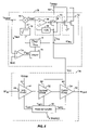
- FIG. 5 illustrates a more detailed block diagram of the power control circuitry providing output power correction for variations in load impedance according to one embodiment of the present invention.
- FIG. 6 illustrates the power control circuitry according to another embodiment of the present invention.
- the present invention is preferably incorporated in a mobile terminal 10 , such a mobile telephone, personal digital assistant, personal computer, or the like.
- the basic architecture of a mobile terminal 10 is represented in FIG. 1 and may include a receiver front end 12 , a radio frequency transmitter section 14 , an antenna 16 , a duplexer or switch 18 , a baseband processor 20 , a control system 22 , a frequency synthesizer 24 , and an interface 26 .
- the receiver front end 12 receives information bearing radio frequency signals from one or more remote transmitters provided by a base station.
- a low noise amplifier 28 amplifies the signal.
- a filter circuit 30 minimizes broadband interference in the received signal, while a downconverter 32 downconverts the filtered, received signal to an intermediate or baseband frequency signal, which is then digitized into one or more digital streams.
- the receiver front end 12 typically uses one or more mixing frequencies generated by the frequency synthesizer 24 .
- the baseband processor 20 processes the digitized received signal to extract the information or data bits conveyed in the received signal. This processing typically comprises demodulation, decoding, and error correction operations. As such, the baseband processor 20 is generally implemented in one or more digital signal processors (DSPs).
- DSPs digital signal processors
- the baseband processor 20 receives digitized data from the control system 22 , which it encodes for transmission.
- the encoded data is output to the radio frequency transmitter section 14 , where it is used by a modulator 34 to modulate a carrier signal that is at a desired transmit frequency.
- Power amplifier circuitry 36 amplifies the modulated carrier signal to a level appropriate for transmission from the antenna 16 .
- a matching network 37 operates to provide optimum power transfer between the power amplifier circuitry 36 and the antenna 16 , as described below in more detail.
- the power amplifier circuitry 36 provides gain for the signal to be transmitted under control of power control circuitry 38 , which is preferably controlled by the control system 22 using an adjustable power control signal (V RAMP ). Further, according to the present invention, the power control circuitry 38 operates to reduce or essentially eliminate variations in output power of the power amplifier circuitry 36 due to variations in the load impedance.
- V RAMP adjustable power control signal
- the modulator 34 may be a polar modulator providing amplitude and phase components of a polar modulation signal.
- the amplitude component may be combined with the adjustable power control signal (V RAMP ), and the combined signal provided to the power control circuitry 38 .
- V RAMP adjustable power control signal
- a polar modulator see commonly owned and assigned U.S. patent application Ser. No. 10/139,560, entitled DIRECT DIGITAL POLAR MODULATOR, filed on May 6, 2002, which is hereby incorporated by reference in its entirety.
- the bias for the power amplifier circuitry 36 is relatively stable regardless of power, and varying the voltage supplied to the power amplifier circuitry 36 controls actual power levels.
- the control system 22 may also provide a transmit enable signal (TX ENABLE) to effectively enable the power amplifier circuitry 36 during periods of transmission.
- a user may interact with the mobile terminal 10 via the interface 26 , which may include interface circuitry 40 associated with a microphone 42 , a speaker 44 , a keypad 46 , and a display 48 .
- the interface circuitry 40 typically includes analog-to-digital converters, digital-to-analog converters, amplifiers, and the like. Additionally, it may include a voice encoder/decoder, in which case it may communicate directly with the baseband processor 20 .
- the microphone 42 will typically convert audio input, such as the user's voice, into an electrical signal, which is then digitized and passed directly or indirectly to the baseband processor 20 . Audio information encoded in the received signal is recovered by the baseband processor 20 , and converted into an analog signal suitable for driving speaker 44 by the I/O and interface circuitry 40 .
- the keypad 46 and display 48 enable the user to interact with the mobile terminal 10 , input numbers to be dialed, address book information, or the like, as well as monitor call progress information.
- the power amplifier circuitry 36 is associated with the power control circuitry 38 .
- the power amplifier circuitry 36 and the power control circuitry 38 are incorporated into a single module.
- the power amplifier circuitry 36 includes three amplifier stages, a first amplifier stage 50 , a second amplifier stage 52 , and a third amplifier stage 54 , as well as a bias network 56 providing bias for each of the three amplifier stages 50 , 52 , 54 .
- the adjustable power control signal (V RAMP ) is received by the power control circuitry 38 and used as a set-point voltage. Based on the adjustable power control signal (V RAMP ), the power control circuitry 38 controls a supply voltage (V CC ) provided to the rails 58 , 60 of the second and third amplifier stages 52 , 54 , respectively. These rails 58 , 60 will typically be the collectors or drains of bipolar or field effect transistors forming the respective amplifier stages, as will be appreciated by those skilled in the art. It should be noted that, in an alternative embodiment, the supply voltage (V CC ) may be provided to the rails 62 , 58 , 60 of the first, second, and third amplifier stages 50 , 52 , 54 . As another alternative, the supply voltage (V CC ) may be provided to the rails 62 , 58 of the first and second amplifier stages 50 , 52 .
- the rail 62 of the first amplifier stage 50 is connected directly to a fixed or primary voltage supply (V PRIM ), which will preferably also be connected to the terminal for the positive potential of a battery.
- the fixed or primary voltage supply (V PRIM ) is also preferably connected to an input terminal 64 of the power control circuitry 38 .
- the bias network 56 supplies a fixed bias to the three amplifier stages 50 , 52 , 54 , regardless of the collector/drain supply voltage (V CC ) provided to the second and third amplifier stages 52 , 54 .
- the fixed bias incorporates traditional V APC signals, which are configured to maintain a constant bias.
- the bias network 56 provides a constant bias to the first amplifier stage 50 and a variable bias that is reduced when the supply voltage (V CC ) is reduced to the second and third amplifier stages 52 , 54 .
- the transmitter control signal (TX ENABLE) is a logic signal used to enable or disable the power amplifier circuitry 36 by removing the bias from each of the three amplifier stages 50 , 52 , 54 .
- a radio frequency signal to be amplified (RF IN ) is provided at the input 66 of the first amplifier stage 50 and amplified by the three amplifier stages 50 , 52 , 54 to provide an amplified output signal (RF OUT ) at the output 68 of the third amplifier stage 54 .
- FIG. 3 The voltage profile of an exemplary V RAMP signal is shown in FIG. 3 .
- the current embodiment of the invention limits the V RAMP signal to +1.8V; however, other embodiments of the invention may use less or more voltage to drive the V RAMP input.
- FIG. 4 the output power level as a function of the V RAMP signal of FIG. 3 is illustrated. Notably, the power level tracks the V RAMP signal and ranges from +5 dBm at the minimum to +35 dBm at the maximum for the preferred embodiment. It should be noted that FIGS. 3 and 4 should be considered exemplary rather than limiting.
- the supply voltage (V CC ) is preferably provided such that the second and third amplifier stages 52 , 54 operate in saturation.
- V PRIM fixed voltage
- the overall output noise power is not increased when the output power of the power amplifier circuitry 36 is decreased.
- FIG. 5 is a detailed schematic of an exemplary embodiment of the power control circuitry 38 of the present invention.
- the power control circuitry 38 includes a voltage regulator 70 , current detection circuitry 72 , an amplifier 74 , delay circuitry 75 , a ratio calculator 76 , a square root extractor 78 , and a multiplier 80 .
- the ratio calculator 76 and the square root extractor 78 are an exemplary embodiment of correction circuitry that, according to the present invention, operates to provide a correction signal to the multiplier 80 based on a comparison of a signal indicative of an actual current (I PA ) provided to the power amplifier circuitry 36 and a signal indicative of a reference current (I REF ).
- the exemplary embodiment of the current detection circuitry 72 includes a resistor 82 and an amplifier 84 .
- the resistor 82 may be a bond wire coupling an output terminal of the power control circuitry 38 to an input of the power amplifier circuitry 36 .
- the resistor 82 may be any resistive element coupling the voltage regulator 70 to the power amplifier circuitry 36 .
- the amplifier 84 operates to provide a voltage ( ⁇ I PA ) indicative of the actual current (I PA ) based on a voltage differential across the resistor 82 .
- the amplifier 74 operates to provide a voltage ( ⁇ I REF ) indicative of a reference current (I REF ) based on amplifying the reference current (I REF ).
- the reference current (I REF ) is a function of the adjustable power control signal (V RAMP ).
- the adjustable power control signal (VAMP) is coupled to a positive terminal (+) of the amplifier 74
- the reference current (I REF ) is the current flowing into the positive terminal (+) of the amplifier 74 .
- the delay circuitry 75 delays the voltage ( ⁇ I REF ) from the amplifier 74 and provides a delayed version of the voltage ( ⁇ I REF ) to the ratio calculator 76 .
- the voltage ( ⁇ I PA ) is also provided to the ratio calculator 76 .
- ⁇ and ⁇ are predetermined such that the voltages ( ⁇ I PA , ⁇ I REF ) are essentially equal when a load impedance (R L ) provided by the matching network 37 ( FIG. 1 ) at the output of the power amplifier circuitry 36 is equal to an ideal load.
- the ideal load may be 1.85 ohms.
- ⁇ and ⁇ are predetermined such that the voltages ( ⁇ I PA , ⁇ I REF ) are essentially equal when the load impedance (R L ) at the output of the power amplifier circuitry 36 is 1.85 ohms.
- the load impedance (R L ) is an impedance seen by the output of the power amplifier circuitry 36 due to the matching network 37 .
- the load impedance (R L ) is often referred to as the power amplifier load line impedance or the power amplifier source impedance.
- the matching network 37 operates to match the load impedance (R L ), which for this example is 1.85 ohms, to a final output impedance seen at the antenna 16 ( FIG.
- the final load impedance seen at the antenna 16 may deviate from the ideal load due to environmental factors such as the antenna 16 touching a user's skin or a foreign metal object.
- the output of the ratio calculator 76 which is referred to herein as a “comparison signal,” is provided to the square root extractor 78 .
- the square root extractor 78 operates to convert the output of the ratio calculator 76 from the power domain (V 2 ) to the voltage domain, which is linear. It should be noted that the square root extractor 76 is implemented such that it calculates the square root of the comparison signal or an approximation thereof.
- the output of the square root extractor 78 which is referred to herein as a “correction signal,” is provided to the multiplier 80 , which operates to multiply the adjustable power control signal (V RAMP ) and the correction signal to provide a corrected adjustable power control signal (V′ RAMP ).
- the power control circuitry 38 operates to reduce or essentially eliminate variations in the output power of the power amplifier circuitry 36 due to variation in the load impedance at the output of the power amplifier circuitry 36 . More specifically, the current detection circuitry 72 generates the voltage ( ⁇ I PA ), which is indicative of the actual current (I PA ), and thus the output power of the power amplifier circuitry 36 .
- the ratio calculator 76 compares the voltage ( ⁇ I PA ) to the voltage ( ⁇ I REF ) to provide a factor (F), which is more generally referred to as the comparison signal.
- the factor (F) is a factor by which the load impedance (R L ) changes from the ideal load, and also a factor by which the value V CC 2 is to be adjusted to correct the output power of the power amplifier circuitry 36 for variations in the load impedance (R L ).
- the load impedance (R L ) is the ideal load, such as 1.85 ohms
- the voltage ( ⁇ I PA ) is essentially equal to the voltage ( ⁇ I REF ) such that the factor (F) output by the ratio calculator 76 is 1.
- the correction signal ( ⁇ square root over (F) ⁇ ) provided by the square root extractor 78 is 1, and the corrected adjustable power control signal (V′ RAMP ) is equal to the adjustable power control signal (V RAMP ).
- the voltage ( ⁇ I PA ) is no longer equal to the voltage ( ⁇ I REF ).
- the load impedance (R L ) is greater than the ideal load, the actual current (I PA ), and thus the voltage ( ⁇ I PA ), decreases.
- the voltage ( ⁇ I PA ) is less than the voltage ( ⁇ I REF ), the factor (F) output by the ratio calculator 76 is greater than 1, and the correction signal ( ⁇ square root over (F) ⁇ ) provided by the square root extractor 78 is also greater than 1.
- the multiplier 80 multiplies the adjustable power control signal (V RAMP ) and the correction signal ( ⁇ square root over (F) ⁇ )
- the corrected adjustable power control signal (V′ RAMP ) is greater than the adjustable power control signal (V RAMP ). Consequently, the supply voltage (V CC ) increases, thereby increasing the actual current (I PA ) such that the voltage ( ⁇ I PA ) is again essentially equal to the voltage ( ⁇ I REF ). As a result, the output power remains essentially equal to the output power for the ideal load.
- the load impedance (R L ) is less than the ideal load, the actual current (I PA ), and thus the voltage ( ⁇ I PA ), increases. Consequently, the voltage ( ⁇ I PA ) is greater than the voltage ( ⁇ I REF ), the factor (F) output by the ratio calculator 76 is less than 1, and the correction signal ( ⁇ square root over (F) ⁇ ) provided by the square root extractor 78 is also less than 1.
- the multiplier 80 multiplies the adjustable power control signal (V RAMP ) and the correction signal ( ⁇ square root over (F) ⁇ )
- the corrected adjustable power control signal (V′ RAMP ) is less than the adjustable power control signal (V RAMP ).
- the operation of the power control circuitry 38 may be mathematically described as follows. The following equations have been simplified for illustrative purposes and easier understanding.
- the actual current (I PA ) is inversely proportional to the load impedance (R L ), which for simplicity is assumed to be a load resistance.
- the load impedance (R L ) is an impedance provided by the matching network 37 ( FIG. 1 ) in order to match the source impedance of the power amplifier circuitry 38 .
- the matching network 37 then provides matching between the load impedance (R L ) and the final load impedance seen at the antenna 16 . As the load impedance (R L ) increases from the ideal load, the actual current (I PA ) decreases.
- the factor (F) by which the load impedance (R L ) has changed is determined by the ratio calculator 76 according to the equation:
- V CC 2 is adjusted by the factor (F), thereby canceling the factor (F) by which the load impedance (R L ) changes.
- the supply voltage (V CC ) is proportional to the adjustable power control signal (V RAMP )
- the supply voltage (V CC ) is adjusted by adjusting the adjustable power control signal (V RAMP ).
- the factor (F) generated by the ratio calculator 76 is provided to the square root extractor 78 , which provides the correction signal ( ⁇ square root over (F) ⁇ ) to the multiplier 80 .
- the supply voltage (V CC ) is multiplied by ⁇ square root over (F) ⁇ , and the supply voltage (V CC ) is adjusted to offset the change in the load impedance (R L ) such that the output power (P OUT ) is essentially equal to the output power (P OUT ) for the ideal load as the load impedance (R L ) varies.
- the output power (P OUT ) of the power amplifier circuitry 36 would also decrease by a factor of 2. Since the actual current (I PA ) decreases by a factor of 2, the ratio ⁇ I REF / ⁇ I PA is 2, the factor (F) output from the ratio calculator 76 is 2, and the correction signal output by the square root extractor 78 is equal to ⁇ square root over (2) ⁇ . As a result, the corrected adjustable power control signal (V′ RAMP ) is equal to ⁇ square root over (2) ⁇ *V RAMP .
- V CC Since the supply voltage (V CC ) is proportional to V RAMP , the supply voltage (V CC ) is also increased by a factor of ⁇ square root over (2) ⁇ . As a result, the value of V CC 2 increases by a factor of 2 such that the output power (P OUT ) is corrected for the variation in the load impedance (R L ). More specifically, by doubling the value of V CC 2 , the doubling of the load impedance (R L ) is cancelled such that the output power (P OUT ) remains constant and is equal to the output power (P OUT ) for the ideal load.
- FIG. 5 also illustrates an exemplary embodiment of the voltage regulator 70 previously disclosed in U.S. Pat. No. 6,701,138, wherein the voltage regulator 70 is a Low Dropout (LDO) voltage regulator.
- LDO Low Dropout
- the voltage regulator 70 includes an error amplifier 86 , a feedback network 88 , and a series pass element 90 .
- the series pass element 90 is a p-FET.
- the corrected adjustable power control signal (V′ RAMP ) may be received by a negative input ( ⁇ ) of an operational amplifier forming the error amplifier 86 .
- the output of the series pass element 90 is fed back through the feedback network 88 and received by positive input (+) of the error amplifier 86 .
- An output signal from error amplifier 86 is provided to a control input of the series pass element 90 that controls the regulated output of voltage regulator 70 .
- the voltage regulator 70 regulates the supply voltage (V CC ) provided to the rails 58 , 60 of the second and third amplifier stages 52 , 54 , respectively.
- the rail 62 of first amplifier stage 50 is connected directly to the fixed or primary voltage supply V PRIM , which will preferably also be connected to the terminal for the positive potential of a battery.
- V PRIM is also preferably provided to the series pass element 90 , as illustrated.
- the bias network 56 preferably supplies a fixed bias to the three power amplifier stages 50 , 52 , 54 , regardless of the collector/drain voltage supplied to the second and third amplifier stages 52 , 54 .
- the voltage regulator 70 may be a switching DC—DC converter, as described in commonly owned and assigned U.S. patent application Ser. No. 10/920,073, entitled POWER AMPLIFIER CONTROL USING A SWITCHING POWER SUPPLY, filed Aug. 17, 2004, which is hereby incorporated herein by reference in its entirety.
- the voltage regulator 70 may be configurable as either an LDO voltage regulator or a switching DC—DC converter, as described in commonly owned and assigned U.S. patent application Ser. No. 11/002,473, entitled RECONFIGURABLE POWER CONTROL FOR A MOBILE TERMINAL, filed Dec. 2, 2004, which is hereby incorporated herein by reference in its entirety.
- FIG. 6 illustrates another embodiment of the power control circuitry 38 of the present invention.
- the current detection circuitry 72 is a current mirror 72 ′.
- the operation of the current mirror 72 ′ will be apparent to one of ordinary skill in the art upon reading this disclosure.
- the current mirror 72 ′ generates the voltage ( ⁇ I PA ) based on the actual current (I PA ) through the series pass element 90 of the voltage regulator 70 .
- the current mirror 72 ′ provides the additional advantage of not adding a voltage drop, such as the voltage drop across the resistor 82 of FIG. 5 , and is easily implemented in CMOS technology.
- the current detection circuitry 72 may be any circuit capable of determining the actual current (I PA ) provided to the power amplifier circuitry 36 .
- the ratio calculator 76 and the square root extractor 78 may alternatively be replaced by correction circuitry that operates to determine the factor (F) by which the load impedance (R L ) has changed and provide the correction signal ( ⁇ square root over (F) ⁇ ) based on a difference between the reference current (I REF ), or some function thereof, and the actual current (I PA ), or some function thereof.
- the elements of the power control circuitry 38 of FIGS. 5 and 6 other than the current detection circuitry 72 , 72 ′ and the voltage regulator 70 may be implemented in the digital domain.
Abstract
Description
Thus, the actual current (IPA) is inversely proportional to the load impedance (RL), which for simplicity is assumed to be a load resistance. As noted above, the load impedance (RL) is an impedance provided by the matching network 37 (
Referring to the equation for the output power (POUT) above, since the output power (POUT) is inversely proportional to the load impedance (RL), the factor (F) by which the load impedance (RL) has changed from the ideal load is the inverse of a factor by which the output power (POUT) of the
Thus, according to the present invention, the value VCC 2 is adjusted by the factor (F), thereby canceling the factor (F) by which the load impedance (RL) changes.
Claims (20)
Priority Applications (1)
| Application Number | Priority Date | Filing Date | Title |
|---|---|---|---|
| US11/245,851 US7109897B1 (en) | 2005-10-07 | 2005-10-07 | Power amplifier control reducing output power variation |
Applications Claiming Priority (1)
| Application Number | Priority Date | Filing Date | Title |
|---|---|---|---|
| US11/245,851 US7109897B1 (en) | 2005-10-07 | 2005-10-07 | Power amplifier control reducing output power variation |
Publications (1)
| Publication Number | Publication Date |
|---|---|
| US7109897B1 true US7109897B1 (en) | 2006-09-19 |
Family
ID=36974506
Family Applications (1)
| Application Number | Title | Priority Date | Filing Date |
|---|---|---|---|
| US11/245,851 Active US7109897B1 (en) | 2005-10-07 | 2005-10-07 | Power amplifier control reducing output power variation |
Country Status (1)
| Country | Link |
|---|---|
| US (1) | US7109897B1 (en) |
Cited By (33)
| Publication number | Priority date | Publication date | Assignee | Title |
|---|---|---|---|---|
| US20050275387A1 (en) * | 2004-06-15 | 2005-12-15 | Semtech Corporation | Method and apparatus for reducing input supply ripple in a DC-DC switching converter |
| US20060205366A1 (en) * | 2005-03-03 | 2006-09-14 | Matsushita Electric Industrial Co., Ltd. | Polar modulation transmission apparatus and wireless communication apparatus |
| US20060255858A1 (en) * | 2005-05-10 | 2006-11-16 | Alps Electric Co., Ltd. | Gain control circuit capable of reducing change in gain due to variation of ambient temperature |
| US20070018621A1 (en) * | 2005-07-22 | 2007-01-25 | The Hong Kong University Of Science And Technology | Area-Efficient Capacitor-Free Low-Dropout Regulator |
| US20070054635A1 (en) * | 2005-09-08 | 2007-03-08 | Black Greg R | Wireless transmitter having polar loop controller with current feedback and methods |
| US20070184795A1 (en) * | 2006-02-03 | 2007-08-09 | Quantance, Inc. | Amplitude error de-glitching circuit and method of operating |
| US20070184794A1 (en) * | 2006-02-03 | 2007-08-09 | Quantance, Inc. | RF Power Amplifier Controller Circuit Including Calibrated Phase Control Loop |
| US20070184792A1 (en) * | 2006-02-03 | 2007-08-09 | Quantance, Inc. | RF Power Amplifier Controller Circuit |
| US20070184793A1 (en) * | 2006-02-03 | 2007-08-09 | Quantance, Inc. | RF Power Amplifier Controller Circuit With Compensation For Output Impedance Mismatch |
| US20070184791A1 (en) * | 2006-02-03 | 2007-08-09 | Vikas Vinayak | Power amplifier controller circuit |
| US20070184796A1 (en) * | 2006-02-03 | 2007-08-09 | Quantance, Inc. | Amplifier compression controller circuit |
| US20070218848A1 (en) * | 2006-02-03 | 2007-09-20 | Quantance, Inc. | Phase error de-glitching circuit and method of operating |
| US20080007231A1 (en) * | 2006-06-05 | 2008-01-10 | Stmicroelectronics Sa | Low drop-out voltage regulator |
| US20080026710A1 (en) * | 2006-07-27 | 2008-01-31 | Harris Corporation | Power management scheme for software-defined radios |
| US20080085684A1 (en) * | 2006-10-06 | 2008-04-10 | Skyworks Solutions, Inc. | Output power correction module for amplifiers in transmitters |
| US20090009241A1 (en) * | 2006-11-21 | 2009-01-08 | Korea Advanced Institute Of Science And Technology | Power amplifier using power combiner |
| US20090081968A1 (en) * | 2007-09-20 | 2009-03-26 | Vikas Vinayak | Power Amplifier Controller With Polar Transmitter |
| EP2045914A1 (en) * | 2006-12-27 | 2009-04-08 | Panasonic Corporation | Polar-modulation transmission device |
| US20090096638A1 (en) * | 2007-10-12 | 2009-04-16 | Olympus Corporation | Encoder |
| US20090117865A1 (en) * | 2007-11-06 | 2009-05-07 | Quantance, Inc. | Rf power amplifier controlled by estimated distortion level of output signal of power amplifier |
| US20090153107A1 (en) * | 2007-12-13 | 2009-06-18 | Marcellus Chen | Method and apparatus for regulating electrical power from a non-perpetual power source |
| US20100194476A1 (en) * | 2009-02-05 | 2010-08-05 | Quantance, Inc. | Amplifier compression adjustment circuit |
| US20100222016A1 (en) * | 2009-03-02 | 2010-09-02 | Fujitsu Limited | Wireless communication device |
| US20120077450A1 (en) * | 2010-09-24 | 2012-03-29 | Emanuel Cohen | Power calibration under voltage standing wave ratio change by frequency sweep |
| US20120126893A1 (en) * | 2009-07-31 | 2012-05-24 | Shingo Yamanouchi | Power amplifier, power amplification method, and storage medium |
| US20120146987A1 (en) * | 2010-12-14 | 2012-06-14 | Getac Technology Corporation | Signal transmitting assembly for cutting off driving signal for driving designated light source and electronic apparatus having the same |
| US20120169424A1 (en) * | 2010-12-30 | 2012-07-05 | Infineon Technologies Ag | Apparatus and Method for Providing Amplifier Linearity Information |
| US8791760B2 (en) | 2011-06-21 | 2014-07-29 | Rf Micro Devices, Inc. | Closed loop bias control |
| US9654074B2 (en) | 2015-05-31 | 2017-05-16 | Mediatek Inc. | Variable gain amplifier circuit, controller of main amplifier and associated control method |
| US9837974B2 (en) | 2015-11-12 | 2017-12-05 | Mediatek Inc. | Amplifier system and method for controlling amplifier |
| US10027300B2 (en) | 2015-11-12 | 2018-07-17 | Mediatek Inc. | Amplifier system, controller of main amplifier and associated control method |
| US20190165747A1 (en) * | 2010-06-07 | 2019-05-30 | Skyworks Solutions, Inc. | Apparatus and method for voltage distribution |
| US20200099341A1 (en) * | 2018-09-21 | 2020-03-26 | Qualcomm Incorporated | Series voltage regulation modulating power supply |
Citations (4)
| Publication number | Priority date | Publication date | Assignee | Title |
|---|---|---|---|---|
| US6665525B2 (en) | 2001-05-29 | 2003-12-16 | Ericsson Inc. | High-level modulation method and apparatus |
| US6701138B2 (en) * | 2001-06-11 | 2004-03-02 | Rf Micro Devices, Inc. | Power amplifier control |
| US6917245B2 (en) * | 2000-09-12 | 2005-07-12 | Silicon Laboratories, Inc. | Absolute power detector |
| US7058374B2 (en) * | 2002-10-15 | 2006-06-06 | Skyworks Solutions, Inc. | Low noise switching voltage regulator |
-
2005
- 2005-10-07 US US11/245,851 patent/US7109897B1/en active Active
Patent Citations (4)
| Publication number | Priority date | Publication date | Assignee | Title |
|---|---|---|---|---|
| US6917245B2 (en) * | 2000-09-12 | 2005-07-12 | Silicon Laboratories, Inc. | Absolute power detector |
| US6665525B2 (en) | 2001-05-29 | 2003-12-16 | Ericsson Inc. | High-level modulation method and apparatus |
| US6701138B2 (en) * | 2001-06-11 | 2004-03-02 | Rf Micro Devices, Inc. | Power amplifier control |
| US7058374B2 (en) * | 2002-10-15 | 2006-06-06 | Skyworks Solutions, Inc. | Low noise switching voltage regulator |
Cited By (80)
| Publication number | Priority date | Publication date | Assignee | Title |
|---|---|---|---|---|
| US7388357B2 (en) * | 2004-06-15 | 2008-06-17 | Semtech Corporation | Method and apparatus for reducing input supply ripple in a DC-DC switching converter |
| US20050275387A1 (en) * | 2004-06-15 | 2005-12-15 | Semtech Corporation | Method and apparatus for reducing input supply ripple in a DC-DC switching converter |
| US20060205366A1 (en) * | 2005-03-03 | 2006-09-14 | Matsushita Electric Industrial Co., Ltd. | Polar modulation transmission apparatus and wireless communication apparatus |
| US7457592B2 (en) * | 2005-03-03 | 2008-11-25 | Panasonic Corporation | Polar modulation transmission apparatus and wireless communication apparatus |
| US20060255858A1 (en) * | 2005-05-10 | 2006-11-16 | Alps Electric Co., Ltd. | Gain control circuit capable of reducing change in gain due to variation of ambient temperature |
| US7400197B2 (en) * | 2005-05-10 | 2008-07-15 | Alps Electric Co., Ltd. | Gain control circuit capable of reducing change in gain due to variation of ambient temperature |
| US20070018621A1 (en) * | 2005-07-22 | 2007-01-25 | The Hong Kong University Of Science And Technology | Area-Efficient Capacitor-Free Low-Dropout Regulator |
| US7495422B2 (en) * | 2005-07-22 | 2009-02-24 | Hong Kong University Of Science And Technology | Area-efficient capacitor-free low-dropout regulator |
| US20070054635A1 (en) * | 2005-09-08 | 2007-03-08 | Black Greg R | Wireless transmitter having polar loop controller with current feedback and methods |
| US7460842B2 (en) | 2005-09-08 | 2008-12-02 | Motorola, Inc. | Wireless transmitter having polar loop controller with current feedback and methods |
| US20070184791A1 (en) * | 2006-02-03 | 2007-08-09 | Vikas Vinayak | Power amplifier controller circuit |
| US7917105B2 (en) | 2006-02-03 | 2011-03-29 | Quantance, Inc. | RF power amplifier controller circuit with compensation for output impedance mismatch |
| US20100301934A1 (en) * | 2006-02-03 | 2010-12-02 | Quantance, Inc. | Rf power amplifier controller circuit with compensation for output impedance mismatch |
| US7869542B2 (en) | 2006-02-03 | 2011-01-11 | Quantance, Inc. | Phase error de-glitching circuit and method of operating |
| US8340604B2 (en) | 2006-02-03 | 2012-12-25 | Quantance, Inc. | RF power amplifier controller circuit including calibrated phase control loop |
| US8260225B2 (en) | 2006-02-03 | 2012-09-04 | Quantance, Inc. | Power amplifier controller circuit |
| US20070184796A1 (en) * | 2006-02-03 | 2007-08-09 | Quantance, Inc. | Amplifier compression controller circuit |
| US20070184793A1 (en) * | 2006-02-03 | 2007-08-09 | Quantance, Inc. | RF Power Amplifier Controller Circuit With Compensation For Output Impedance Mismatch |
| US20070184792A1 (en) * | 2006-02-03 | 2007-08-09 | Quantance, Inc. | RF Power Amplifier Controller Circuit |
| US20070184794A1 (en) * | 2006-02-03 | 2007-08-09 | Quantance, Inc. | RF Power Amplifier Controller Circuit Including Calibrated Phase Control Loop |
| US8238853B2 (en) | 2006-02-03 | 2012-08-07 | Quantance, Inc. | Amplitude error de-glitching circuit and method of operating |
| US20070184795A1 (en) * | 2006-02-03 | 2007-08-09 | Quantance, Inc. | Amplitude error de-glitching circuit and method of operating |
| US8208876B2 (en) | 2006-02-03 | 2012-06-26 | Quantance, Inc. | Amplifier compression controller circuit |
| US8179994B2 (en) | 2006-02-03 | 2012-05-15 | Quantance, Inc. | Phase error de-glitching circuit and method of operating |
| US8095090B2 (en) | 2006-02-03 | 2012-01-10 | Quantance, Inc. | RF power amplifier controller circuit |
| US20100201402A1 (en) * | 2006-02-03 | 2010-08-12 | Quantance, Inc. | Phase Error De-Glitching Circuit and Method of Operating |
| US8032097B2 (en) | 2006-02-03 | 2011-10-04 | Quantance, Inc. | Amplitude error de-glitching circuit and method of operating |
| US20110189966A1 (en) * | 2006-02-03 | 2011-08-04 | Quantance, Inc. | Power Amplifier Controller Circuit |
| US20110140777A1 (en) * | 2006-02-03 | 2011-06-16 | Quantance, Inc. | RF Power Amplifier Controller Circuit Including Calibrated Phase Control Loop |
| US20100194440A1 (en) * | 2006-02-03 | 2010-08-05 | Quantance, Inc. | Phase Error De-Glitching Circuit and Method of Operating |
| US7933570B2 (en) | 2006-02-03 | 2011-04-26 | Quantance, Inc. | Power amplifier controller circuit |
| US7917106B2 (en) | 2006-02-03 | 2011-03-29 | Quantance, Inc. | RF power amplifier controller circuit including calibrated phase control loop |
| US20070218848A1 (en) * | 2006-02-03 | 2007-09-20 | Quantance, Inc. | Phase error de-glitching circuit and method of operating |
| US7761065B2 (en) | 2006-02-03 | 2010-07-20 | Quantance, Inc. | RF power amplifier controller circuit with compensation for output impedance mismatch |
| US7876853B2 (en) | 2006-02-03 | 2011-01-25 | Quantance, Inc. | Phase error de-glitching circuit and method of operating |
| US8044653B2 (en) * | 2006-06-05 | 2011-10-25 | Stmicroelectronics Sa | Low drop-out voltage regulator |
| US20080007231A1 (en) * | 2006-06-05 | 2008-01-10 | Stmicroelectronics Sa | Low drop-out voltage regulator |
| US7590395B2 (en) * | 2006-07-27 | 2009-09-15 | Harris Corporation | Power management scheme for software-defined radios |
| US20080026710A1 (en) * | 2006-07-27 | 2008-01-31 | Harris Corporation | Power management scheme for software-defined radios |
| US20100248657A1 (en) * | 2006-10-06 | 2010-09-30 | Phillips Kerry B | Power correction module for power amplifiers |
| EP2070278A2 (en) * | 2006-10-06 | 2009-06-17 | Skyworks Solutions, Inc. | Output power correction module for amplifiers in transmitters |
| US8369803B2 (en) | 2006-10-06 | 2013-02-05 | Skyworks Solutions, Inc. | Power correction module for power amplifiers |
| US20080085684A1 (en) * | 2006-10-06 | 2008-04-10 | Skyworks Solutions, Inc. | Output power correction module for amplifiers in transmitters |
| WO2008045159A2 (en) | 2006-10-06 | 2008-04-17 | Skyworks Solutions, Inc. | Output power correction module for amplifiers in transmitters |
| EP2070278A4 (en) * | 2006-10-06 | 2009-11-11 | Skyworks Solutions Inc | Output power correction module for amplifiers in transmitters |
| US7937049B2 (en) | 2006-10-06 | 2011-05-03 | Skyworks Solutions, Inc. | Output power correction module for amplifiers in transmitters |
| US20090009241A1 (en) * | 2006-11-21 | 2009-01-08 | Korea Advanced Institute Of Science And Technology | Power amplifier using power combiner |
| US7592865B2 (en) | 2006-11-21 | 2009-09-22 | Korea Advanced Institute Of Science And Technology | Power amplifier using power combiner |
| CN101188404B (en) * | 2006-11-21 | 2011-06-01 | 韩国科学技术院 | Power amplifier using power synthesizer |
| EP2045914A4 (en) * | 2006-12-27 | 2014-03-05 | Panasonic Corp | Polar-modulation transmission device |
| EP2045914A1 (en) * | 2006-12-27 | 2009-04-08 | Panasonic Corporation | Polar-modulation transmission device |
| US20090081968A1 (en) * | 2007-09-20 | 2009-03-26 | Vikas Vinayak | Power Amplifier Controller With Polar Transmitter |
| US8050638B2 (en) | 2007-09-20 | 2011-11-01 | Quantance, Inc. | Power amplifier controller with polar transmitter |
| US7783269B2 (en) | 2007-09-20 | 2010-08-24 | Quantance, Inc. | Power amplifier controller with polar transmitter |
| US20100311365A1 (en) * | 2007-09-20 | 2010-12-09 | Quantance, Inc. | Power Amplifier Controller With Polar Transmitter |
| US7705751B2 (en) * | 2007-10-12 | 2010-04-27 | Olympus Corporation | Encoder |
| US20090096638A1 (en) * | 2007-10-12 | 2009-04-16 | Olympus Corporation | Encoder |
| WO2009061583A1 (en) * | 2007-11-06 | 2009-05-14 | Quantance, Inc. | Rf power amplifier controlled by estimated distortion level of output signal of power amplifier |
| US20090117865A1 (en) * | 2007-11-06 | 2009-05-07 | Quantance, Inc. | Rf power amplifier controlled by estimated distortion level of output signal of power amplifier |
| US8014735B2 (en) | 2007-11-06 | 2011-09-06 | Quantance, Inc. | RF power amplifier controlled by estimated distortion level of output signal of power amplifier |
| US20090153107A1 (en) * | 2007-12-13 | 2009-06-18 | Marcellus Chen | Method and apparatus for regulating electrical power from a non-perpetual power source |
| US7777566B1 (en) | 2009-02-05 | 2010-08-17 | Quantance, Inc. | Amplifier compression adjustment circuit |
| US20100194476A1 (en) * | 2009-02-05 | 2010-08-05 | Quantance, Inc. | Amplifier compression adjustment circuit |
| US20100222016A1 (en) * | 2009-03-02 | 2010-09-02 | Fujitsu Limited | Wireless communication device |
| US20120126893A1 (en) * | 2009-07-31 | 2012-05-24 | Shingo Yamanouchi | Power amplifier, power amplification method, and storage medium |
| US8594589B2 (en) * | 2009-07-31 | 2013-11-26 | Nec Corporation | Power amplifier, power amplification method, and storage medium |
| US20190165747A1 (en) * | 2010-06-07 | 2019-05-30 | Skyworks Solutions, Inc. | Apparatus and method for voltage distribution |
| US8364104B2 (en) * | 2010-09-24 | 2013-01-29 | Intel Corporation | Power calibration under voltage standing wave ratio change by frequency sweep |
| US20120077450A1 (en) * | 2010-09-24 | 2012-03-29 | Emanuel Cohen | Power calibration under voltage standing wave ratio change by frequency sweep |
| US20120146987A1 (en) * | 2010-12-14 | 2012-06-14 | Getac Technology Corporation | Signal transmitting assembly for cutting off driving signal for driving designated light source and electronic apparatus having the same |
| US9083326B2 (en) * | 2010-12-14 | 2015-07-14 | Getac Technology Corporation | Signal transmitting assembly for cutting off driving signal for driving designated light source and electronic apparatus having the same |
| US8912851B2 (en) * | 2010-12-30 | 2014-12-16 | Intel Mobile Communications GmbH | Apparatus and method for providing amplifier linearity information |
| US20120169424A1 (en) * | 2010-12-30 | 2012-07-05 | Infineon Technologies Ag | Apparatus and Method for Providing Amplifier Linearity Information |
| US8791760B2 (en) | 2011-06-21 | 2014-07-29 | Rf Micro Devices, Inc. | Closed loop bias control |
| US9654074B2 (en) | 2015-05-31 | 2017-05-16 | Mediatek Inc. | Variable gain amplifier circuit, controller of main amplifier and associated control method |
| US9837974B2 (en) | 2015-11-12 | 2017-12-05 | Mediatek Inc. | Amplifier system and method for controlling amplifier |
| US10027300B2 (en) | 2015-11-12 | 2018-07-17 | Mediatek Inc. | Amplifier system, controller of main amplifier and associated control method |
| US10263585B2 (en) | 2015-11-12 | 2019-04-16 | Mediatek Inc. | Amplifier system and method for controlling amplifier |
| US20200099341A1 (en) * | 2018-09-21 | 2020-03-26 | Qualcomm Incorporated | Series voltage regulation modulating power supply |
| US10749477B2 (en) * | 2018-09-21 | 2020-08-18 | Qualcomm Incorporated | Series voltage regulation modulating power supply |
Similar Documents
| Publication | Publication Date | Title |
|---|---|---|
| US7109897B1 (en) | Power amplifier control reducing output power variation | |
| US6701138B2 (en) | Power amplifier control | |
| US7777566B1 (en) | Amplifier compression adjustment circuit | |
| US7917106B2 (en) | RF power amplifier controller circuit including calibrated phase control loop | |
| US7193459B1 (en) | Power amplifier control technique for enhanced efficiency | |
| US8260225B2 (en) | Power amplifier controller circuit | |
| US7340235B1 (en) | System for limiting current in an output stage of a power amplifier | |
| US9257941B2 (en) | Adaptive biasing scheme for an amplifier | |
| US8095090B2 (en) | RF power amplifier controller circuit | |
| US8018277B2 (en) | RF power amplifier system with impedance modulation | |
| US20040174213A1 (en) | Doherty bias circuit to dynamically compensate for process and environmental variations | |
| US20070184796A1 (en) | Amplifier compression controller circuit | |
| US20100301934A1 (en) | Rf power amplifier controller circuit with compensation for output impedance mismatch | |
| US20090021303A1 (en) | Distortion-Driven Power Amplifier Power Supply Controller | |
| US8791760B2 (en) | Closed loop bias control | |
| US8884703B2 (en) | VRAMP limiting using resistors | |
| US6731173B1 (en) | Doherty bias circuit to dynamically compensate for process and environmental variations | |
| US7315152B1 (en) | System for detecting current in an output stage of a power amplifier | |
| US8432228B1 (en) | Power control circuit for radio frequency power amplifiers | |
| US8653891B2 (en) | Collector boost |
Legal Events
| Date | Code | Title | Description |
|---|---|---|---|
| AS | Assignment |
Owner name: RF MICRO DEVICES, INC., NORTH CAROLINA Free format text: ASSIGNMENT OF ASSIGNORS INTEREST;ASSIGNOR:LEVESQUE, CHRIS;REEL/FRAME:017081/0189 Effective date: 20050627 |
|
| STCF | Information on status: patent grant |
Free format text: PATENTED CASE |
|
| FPAY | Fee payment |
Year of fee payment: 4 |
|
| AS | Assignment |
Owner name: BANK OF AMERICA, N.A., AS ADMINISTRATIVE AGENT, TE Free format text: NOTICE OF GRANT OF SECURITY INTEREST IN PATENTS;ASSIGNOR:RF MICRO DEVICES, INC.;REEL/FRAME:030045/0831 Effective date: 20130319 |
|
| FPAY | Fee payment |
Year of fee payment: 8 |
|
| AS | Assignment |
Owner name: RF MICRO DEVICES, INC., NORTH CAROLINA Free format text: TERMINATION AND RELEASE OF SECURITY INTEREST IN PATENTS (RECORDED 3/19/13 AT REEL/FRAME 030045/0831);ASSIGNOR:BANK OF AMERICA, N.A., AS ADMINISTRATIVE AGENT;REEL/FRAME:035334/0363 Effective date: 20150326 |
|
| AS | Assignment |
Owner name: QORVO US, INC., NORTH CAROLINA Free format text: MERGER;ASSIGNOR:RF MICRO DEVICES, INC.;REEL/FRAME:039196/0941 Effective date: 20160330 |
|
| FEPP | Fee payment procedure |
Free format text: MAINTENANCE FEE REMINDER MAILED (ORIGINAL EVENT CODE: REM.) |
|
| FEPP | Fee payment procedure |
Free format text: 11.5 YR SURCHARGE- LATE PMT W/IN 6 MO, LARGE ENTITY (ORIGINAL EVENT CODE: M1556); ENTITY STATUS OF PATENT OWNER: LARGE ENTITY |
|
| MAFP | Maintenance fee payment |
Free format text: PAYMENT OF MAINTENANCE FEE, 12TH YEAR, LARGE ENTITY (ORIGINAL EVENT CODE: M1553); ENTITY STATUS OF PATENT OWNER: LARGE ENTITY Year of fee payment: 12 |