US7115821B1 - Laser module carrier for printed circuit boards - Google Patents
Laser module carrier for printed circuit boards Download PDFInfo
- Publication number
- US7115821B1 US7115821B1 US10/681,871 US68187103A US7115821B1 US 7115821 B1 US7115821 B1 US 7115821B1 US 68187103 A US68187103 A US 68187103A US 7115821 B1 US7115821 B1 US 7115821B1
- Authority
- US
- United States
- Prior art keywords
- carrier
- sides
- laser module
- frame
- circuit board
- Prior art date
- Legal status (The legal status is an assumption and is not a legal conclusion. Google has not performed a legal analysis and makes no representation as to the accuracy of the status listed.)
- Expired - Fee Related, expires
Links
- 239000000835 fiber Substances 0.000 claims abstract description 25
- 239000013307 optical fiber Substances 0.000 claims abstract description 11
- ALFHIHDQSYXSGP-UHFFFAOYSA-N 1,2-dichloro-3-(2,4-dichlorophenyl)benzene Chemical compound ClC1=CC(Cl)=CC=C1C1=CC=CC(Cl)=C1Cl ALFHIHDQSYXSGP-UHFFFAOYSA-N 0.000 description 23
- 238000004891 communication Methods 0.000 description 3
- 238000000034 method Methods 0.000 description 3
- 230000003287 optical effect Effects 0.000 description 3
- 238000005452 bending Methods 0.000 description 2
- RNFJDJUURJAICM-UHFFFAOYSA-N 2,2,4,4,6,6-hexaphenoxy-1,3,5-triaza-2$l^{5},4$l^{5},6$l^{5}-triphosphacyclohexa-1,3,5-triene Chemical compound N=1P(OC=2C=CC=CC=2)(OC=2C=CC=CC=2)=NP(OC=2C=CC=CC=2)(OC=2C=CC=CC=2)=NP=1(OC=1C=CC=CC=1)OC1=CC=CC=C1 RNFJDJUURJAICM-UHFFFAOYSA-N 0.000 description 1
- 239000004593 Epoxy Substances 0.000 description 1
- 230000002411 adverse Effects 0.000 description 1
- 230000015556 catabolic process Effects 0.000 description 1
- 238000010276 construction Methods 0.000 description 1
- 238000006731 degradation reaction Methods 0.000 description 1
- 230000000593 degrading effect Effects 0.000 description 1
- 239000003063 flame retardant Substances 0.000 description 1
- 230000001939 inductive effect Effects 0.000 description 1
- 238000004806 packaging method and process Methods 0.000 description 1
- 239000004033 plastic Substances 0.000 description 1
- 239000004417 polycarbonate Substances 0.000 description 1
- 229920000515 polycarbonate Polymers 0.000 description 1
- 239000011347 resin Substances 0.000 description 1
- 229920005989 resin Polymers 0.000 description 1
- 238000000926 separation method Methods 0.000 description 1
- 229910000679 solder Inorganic materials 0.000 description 1
Images


Classifications
-
- G—PHYSICS
- G02—OPTICS
- G02B—OPTICAL ELEMENTS, SYSTEMS OR APPARATUS
- G02B6/00—Light guides; Structural details of arrangements comprising light guides and other optical elements, e.g. couplings
- G02B6/24—Coupling light guides
- G02B6/42—Coupling light guides with opto-electronic elements
- G02B6/4201—Packages, e.g. shape, construction, internal or external details
- G02B6/4266—Thermal aspects, temperature control or temperature monitoring
- G02B6/4268—Cooling
- G02B6/4269—Cooling with heat sinks or radiation fins
-
- G—PHYSICS
- G02—OPTICS
- G02B—OPTICAL ELEMENTS, SYSTEMS OR APPARATUS
- G02B6/00—Light guides; Structural details of arrangements comprising light guides and other optical elements, e.g. couplings
- G02B6/24—Coupling light guides
- G02B6/42—Coupling light guides with opto-electronic elements
- G02B6/4201—Packages, e.g. shape, construction, internal or external details
- G02B6/4266—Thermal aspects, temperature control or temperature monitoring
- G02B6/4268—Cooling
- G02B6/4271—Cooling with thermo electric cooling
-
- G—PHYSICS
- G02—OPTICS
- G02B—OPTICAL ELEMENTS, SYSTEMS OR APPARATUS
- G02B6/00—Light guides; Structural details of arrangements comprising light guides and other optical elements, e.g. couplings
- G02B6/24—Coupling light guides
- G02B6/42—Coupling light guides with opto-electronic elements
- G02B6/4201—Packages, e.g. shape, construction, internal or external details
- G02B6/4274—Electrical aspects
- G02B6/428—Electrical aspects containing printed circuit boards [PCB]
-
- G—PHYSICS
- G02—OPTICS
- G02B—OPTICAL ELEMENTS, SYSTEMS OR APPARATUS
- G02B6/00—Light guides; Structural details of arrangements comprising light guides and other optical elements, e.g. couplings
- G02B6/44—Mechanical structures for providing tensile strength and external protection for fibres, e.g. optical transmission cables
- G02B6/4439—Auxiliary devices
- G02B6/4471—Terminating devices ; Cable clamps
- G02B6/4478—Bending relief means
Definitions
- the invention relates generally to the mounting of electronic components to circuit boards.
- the invention relates to a carrier apparatus for mounting a laser module to a printed circuit board.
- Dense wavelength division multiplexing (DWDM) systems includes lasers which require precise and accurate temperature control for satisfactory performance.
- Each laser is typically integrated in a package or laser module which is mounted to a printed circuit board (PCB).
- PCB printed circuit board
- heat sinks were mounted directly to the laser modules to remove excess heat.
- the long flexible wire leads extending from the laser module were sufficient to accommodate the dimensional tolerances of mounting holes used to mount the laser module to the heat sink, of mounting holes in the PCB for mounting the heat sink to the PCB, and of the solder pads or holes for connection of the laser module leads to the PCB.
- the positions of the leads extending from the laser module cannot be disturbed without adversely affecting the electrical characteristics of the laser module and PCB. For example, bending or flexing the leads during the process of mounting the laser module to the PCB can cause signal loss. In addition, the leads cannot be misaligned to the tracks on the PCB without degrading the electrical signals. Moreover, a heat sink mounted directly to the laser module can generate stress sufficient to break the leads.
- the present invention satisfies this need and provides additional advantages.
- the invention features a carrier for alignment and attachment of an electronics module having a plurality of leads to a circuit board.
- the carrier includes a frame and an alignment guide disposed on the frame to align the electronics module to the carrier.
- the frame includes a plurality of sides defining a region to receive the electronics module.
- the frame has a gap between two of the sides for passage of the leads from the electronics module. At least one of the sides has a first surface configured to maintain contact with a surface of the electronics module when the electronics module is secured to the frame. At least one of the sides has a second surface configured to maintain contact with a first surface of the circuit board when the carrier is secured to the circuit board.
- the carrier also includes an alignment guide disposed on the frame to align the frame to the circuit board.
- the carrier also includes a capture device disposed on one of the sides of the frame to secure the electronics module to the frame.
- the carrier also includes a fiber guide or a wire guide extending from one of the sides opposite the region to receive the electronics module.
- the invention features a carrier for attachment of a laser module having a plurality of leads to a circuit board.
- the carrier includes a frame having a first side, a second side and a third side in a C-shaped configuration. At least one of the sides has a first surface, at least one of the sides has a second surface and at least one of the sides has an opening to receive a board fastener.
- the first and second surfaces are separated by a predetermined distance so that the leads of the laser module are positioned substantially along a surface of the circuit board when the laser module is secured to the carrier and the carrier is secured to the circuit board.
- the carrier also includes a first plurality of alignment posts disposed on the first surfaces and a second plurality of alignment posts disposed on the second surfaces.
- the carrier also includes a capture clip disposed on one of the sides to secure the laser module to the frame and a fiber guide extending from one of the sides.
- FIG. 1 is an illustration of a laser diode module used in DWDM communication systems.
- FIG. 2 is an illustration of an embodiment of a carrier for attaching a laser module to a circuit board in accordance with the principles of the invention.
- FIG. 3A and FIG. 3B are top and bottom views, respectively, of an embodiment of a carrier for attaching a laser module to a circuit board in accordance with the principles of the invention.
- FIG. 4A , FIG. 4B and FIG. 4C are top, side and bottom views, respectively, of the carrier of FIG. 3A and FIG. 3B showing exemplary dimensions.
- FIG. 5 is an illustration of a laser module attached to the carrier of FIG. 3A and FIG. 3B .
- FIG. 6 shows the alignment of features on the carrier of FIGS. 3A and 3B to a printed circuit board prior to attachment.
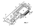
- FIG. 7 is an illustration of a bottom view of the carrier of FIGS. 3A and 3B after attachment to a printed circuit board.
- the present invention relates to a carrier for accurately positioning and securing an electronics module to a circuit board.
- the carrier includes a frame having sides that surround a capture region. The sides include holes to pass mounting screws used to secure the carrier to the circuit board. Alignment posts extending from the upper surface of the sides of the frame engage holes in the electronics component packaging to accurately position the electronics component within the plane of the capture region. Alignment posts extending from the upper surface of one or more sides of the frame engage holes in the circuit board to ensure accurate positioning of the carrier to the circuit board.
- One of the sides also includes a capture device to eliminate movement of the electronics module in a direction normal to the plane of the capture region.
- FIG. 1 depicts a laser module 10 used for dense wavelength division multiplexing (DWDM) communications.
- the laser module 10 includes a laser, a thermoelectric cooler and other electrical and/or optical internal components.
- Flanged portions 18 extend from opposite ends of the laser module 10 .
- the flanged portions 18 include holes 22 and notches 26 used for mounting the laser module 10 to a circuit board such as a printed circuit board (PCB).
- Optical signals generated by the internal laser are transmitted through an optical fiber 30 extending from the laser module 10 .
- a fiber boot 34 extending through one end of the laser module 10 substantially eliminates stress on the optical fiber 30 that might otherwise be induced at the region where the optical fiber 30 contacts the laser module 10 .
- Electrodes 36 extend out from a side 14 of the laser module 10 . These leads 36 apply various voltages and/or supply current to the internal components of the laser module 10 . For example, the voltages can be used to electrically bias the laser and to power the thermoelectric cooler. In addition one or more leads 36 can be used to provide data signals to the laser.
- the leads 36 are generally fragile and can be fractured if excessive stress is applied. Moreover, if the leads 36 are disturbed from their nominal position, their electrical characteristics can change, leading to degradation in the performance of the laser module 10 , especially at high data rates.
- FIG. 2 illustrates the laser module 10 secured to a carrier 38 in accordance with the principles of the invention.
- the carrier 38 is shown below a PCB 42 prior to mounting.
- An opening 46 in the PCB 42 is shaped to accept the laser module 10 and carrier 38 , and to allow the leads (not visible) of the laser module 10 to extend over a surface 50 ′ or 50 ′′ (generally 50 ) of the PCB 42 .
- alignment holes 48 in the PCB 42 are used to achieve accurate lateral positioning of the laser module 10 in the plane of the PCB 42 .
- FIG. 3A and FIG. 3B illustrate top and bottom views, respectively, of a carrier 38 constructed according to the principles of the invention.
- the carrier 38 includes a frame 52 having three sides 54 ′, 54 ′′ and 54 ′′′ (generally 54 ) arranged in the shape of the letter “C”.
- the frame 52 can be fabricated from flame retardant polycarbonate plastic.
- the sides 54 substantially surround a region 58 that receives the laser module.
- An open portion, or gap, in the frame 52 (between ends of opposing sides 54 ′ and 54 ′′′) prevents interference between the frame 52 and the module leads.
- the opposing sides 54 ′, 54 ′′′ include four module alignment posts 62 that extend normal to upper surfaces 66 of the sides 54 ′, 54 ′′′.
- module alignment posts 62 act as an alignment guide and allow for accurate lateral positioning of the laser module in the carrier 38 .
- Two of the sides 54 ′′, 54 ′′′ have board alignment posts 70 extending normal to their respective lower surfaces 74 .
- the board alignment posts 70 serve as an alignment guide and ensure accurate positioning of the carrier 38 to the PCB 42 .
- the module alignment posts 62 and/or the board alignment posts 70 are located on just one side 54 of the frame or all three sides 54 of the frame.
- the upper and lower surfaces 66 and 74 are fabricated according to strict dimensional tolerances of few thousands of an inch such that the vertical separation of the surfaces 66 , 74 provides accurate vertical positioning (i.e., along an axis normal to the PCB surfaces) within the opening 46 in the PCB 42 when the carrier 38 is mounted.
- the leads 36 extending from the laser module 10 lie along or just above a surface 50 of the PCB 42 .
- the leads 36 can be soldered or otherwise electrically coupled to the PCB 42 without bending or flexing.
- the frame 52 includes a capture device 76 on one side 54 ′ for securing the laser module to the carrier 38 .
- the capture device 76 is a clip having a resilient stem 78 extending normal to the plane of the frame 52 .
- the stem 78 terminates at a tab 80 that extends laterally towards the region 58 in the frame 52 .
- the sides 54 of the frame 52 include holes 82 to receive board fasteners for securing the carrier 38 to the PCB 42 .
- the board fasteners can be, for example, screws which pass through openings in the PCB 42 and holes 82 in the frame 52 . The screws form threads in the holes 82 when they are first inserted.
- the carrier 38 includes a fiber guide 86 that extends normal to one side 54 ′′′ away from the region 58 .
- the fiber guide 86 provides a means to safely secure the optical fiber 30 where the optical fiber 30 extends from the laser module 10 without inducing undesirable stress.
- the fiber guide 86 includes an elongated portion 88 having a channel to pass and substantially encompass the boot 34 of the optical fiber 30 .
- a fiber clip 90 at the end of the elongated portion 88 opposite the frame 52 is used to grip a portion of the fiber boot 34 .
- a wire guide extends from the frame 52 in place of the fiber guide 86 .
- the wire guide is similar in construction and function to the fiber guide 86 in that the wire guide secures one or more wires, or cables, that extend from the electronics module and pass through a boot.
- FIG. 4A , FIG. 4B and FIG. 4C illustrate a top, a side and a bottom view, respectively, of the carrier 38 of FIG. 3A and FIG. 3B with exemplary dimensions shown in millimeters. It should be recognized that the indicated dimensions refer to a certain laser module and PCB configuration. One of skill in the art will recognize that the dimensions of the carrier 38 can be varied according to the dimensions and features of the specific laser module (or electronics module) and circuit board.
- the optical fiber 30 is inserted into the fiber guide 86 with sufficient slack to allow the laser module 10 to be easily manipulated within the carrier region 58 .
- the laser module 10 is then inserted through the region 58 in the carrier 38 from underneath (i.e., up from underneath in FIG. 3A ) until the laser module 10 is above the carrier 38 .
- the laser module 10 is accurately laterally positioned on the carrier 38 .
- the resilient stem 78 of the capture device 76 is urged away from the adjacent flange 18 .
- the resilient stem 78 returns (i.e., snaps) back to its original position.
- the tab 80 applies pressure to the top of the laser module 10 to secure it vertically to the carrier 38 .
- the optical fiber 30 is then fed through the elongated portion 88 of the cable guide 86 until a portion of the fiber boot 34 is adjacent the fiber clip 90 .
- FIG. 5 illustrates the laser module 10 mounted to the carrier 38 after the attachment process is completed.
- FIG. 6 shows a top view of the alignment of features on the carrier 38 to the PCB 42 .
- FIG. 7 illustrates a bottom view of the carrier 38 mounted to the PCB 42 .
- attaching the carrier 38 to the PCB 42 includes moving the laser module 10 upward (in FIG. 6 ) so that the laser module 10 extends into the opening 46 in the PCB 42 .
- a notch 98 at one end of the PCB opening 46 provides clearance for the stem 78 of the capture device.
- the board alignment pins 70 engage the alignment holes 48 when the carrier 38 is properly laterally positioned with respect to the PCB 42 .
- Screws 102 (only one shown) are inserted through respective notches 106 along the edge of the PCB opening 46 .
- the screws 102 extend through the holes 82 in the frame 52 .
- the screws form threads in the holes 82 when they are first inserted.
- the screws 102 loosely hold the carrier 38 in place during alignment to the PCB 42 and while the leads 36 are soldered to the PCB contacts.
- the screws 102 are then tightened to secure the carrier 38 in place.
- the lower surfaces 74 of the sides 54 ′′, 54 ′′′ are maintained in contact with the lower surface 50 ′′ of the PCB 42 .
- a heat sink for removal of excess heat from the laser module can be mounted directly to the PCB 42 .
- strict dimensional tolerances result in accurate vertical positioning of the laser module 10 to the PCB 42 .
- a surface of the heat sink can be mounted directly to the PCB 42 so that the surface of the heat sink is in close proximity with an upper surface of the laser module 10 .
- a thermal epoxy/resin is used to ensure full contact between the heat sink and the laser module 10 .
- the laser module 10 does not have to support the weight of the heat sink and no significant stress is imparted to the leads 36 extending from the laser module 10 .
Abstract
Description
Claims (6)
Priority Applications (1)
| Application Number | Priority Date | Filing Date | Title |
|---|---|---|---|
| US10/681,871 US7115821B1 (en) | 2003-10-08 | 2003-10-08 | Laser module carrier for printed circuit boards |
Applications Claiming Priority (1)
| Application Number | Priority Date | Filing Date | Title |
|---|---|---|---|
| US10/681,871 US7115821B1 (en) | 2003-10-08 | 2003-10-08 | Laser module carrier for printed circuit boards |
Publications (1)
| Publication Number | Publication Date |
|---|---|
| US7115821B1 true US7115821B1 (en) | 2006-10-03 |
Family
ID=37037255
Family Applications (1)
| Application Number | Title | Priority Date | Filing Date |
|---|---|---|---|
| US10/681,871 Expired - Fee Related US7115821B1 (en) | 2003-10-08 | 2003-10-08 | Laser module carrier for printed circuit boards |
Country Status (1)
| Country | Link |
|---|---|
| US (1) | US7115821B1 (en) |
Cited By (3)
| Publication number | Priority date | Publication date | Assignee | Title |
|---|---|---|---|---|
| WO2014062502A1 (en) * | 2012-10-18 | 2014-04-24 | Corning Cable Systems Llc | Cable bend relief for fiber optic cable sub-assemblies and methods of assembling |
| US20170069990A1 (en) * | 2015-09-08 | 2017-03-09 | Ross Video Limited | Circuit board pad layout and mechanical retainer |
| US20220326455A1 (en) * | 2019-09-18 | 2022-10-13 | Nippon Telegraph And Telephone Corporation | Package for Optical Module |
Citations (4)
| Publication number | Priority date | Publication date | Assignee | Title |
|---|---|---|---|---|
| US4858067A (en) * | 1987-11-18 | 1989-08-15 | Crl Electronics, Inc. | Modular electronic control housing assembly |
| US5805423A (en) * | 1996-05-17 | 1998-09-08 | United Technologies Automotive | Battery contact and retention apparatus for printed circuit boards |
| US6184462B1 (en) * | 1998-06-29 | 2001-02-06 | Caterpillar Inc. | Apparatus for retaining a printed circuit board |
| US6275388B1 (en) * | 1998-07-08 | 2001-08-14 | Welch Allyn Data Collection, Inc. | Image sensor mounting system |
-
2003
- 2003-10-08 US US10/681,871 patent/US7115821B1/en not_active Expired - Fee Related
Patent Citations (4)
| Publication number | Priority date | Publication date | Assignee | Title |
|---|---|---|---|---|
| US4858067A (en) * | 1987-11-18 | 1989-08-15 | Crl Electronics, Inc. | Modular electronic control housing assembly |
| US5805423A (en) * | 1996-05-17 | 1998-09-08 | United Technologies Automotive | Battery contact and retention apparatus for printed circuit boards |
| US6184462B1 (en) * | 1998-06-29 | 2001-02-06 | Caterpillar Inc. | Apparatus for retaining a printed circuit board |
| US6275388B1 (en) * | 1998-07-08 | 2001-08-14 | Welch Allyn Data Collection, Inc. | Image sensor mounting system |
Cited By (6)
| Publication number | Priority date | Publication date | Assignee | Title |
|---|---|---|---|---|
| WO2014062502A1 (en) * | 2012-10-18 | 2014-04-24 | Corning Cable Systems Llc | Cable bend relief for fiber optic cable sub-assemblies and methods of assembling |
| US9310572B2 (en) | 2012-10-18 | 2016-04-12 | Corning Cable Systems Llc | Cable bend relief for fiber optic sub-assemblies and methods of assembling |
| US20170069990A1 (en) * | 2015-09-08 | 2017-03-09 | Ross Video Limited | Circuit board pad layout and mechanical retainer |
| US9799973B2 (en) * | 2015-09-08 | 2017-10-24 | Ross Video Limited | Circuit board pad layout and mechanical retainer |
| US20220326455A1 (en) * | 2019-09-18 | 2022-10-13 | Nippon Telegraph And Telephone Corporation | Package for Optical Module |
| US11768341B2 (en) * | 2019-09-18 | 2023-09-26 | Nippon Telegraph And Telephone Corporation | Package for optical module |
Similar Documents
| Publication | Publication Date | Title |
|---|---|---|
| US6583902B1 (en) | Modular fiber-optic transceiver | |
| US7872278B2 (en) | Light emitting diode system, method for producing such a system, and backlighting device | |
| US8047856B2 (en) | Array connector for optical transceiver module | |
| US7478955B2 (en) | Modular laser package system | |
| JP5184708B1 (en) | Optical module | |
| US6590152B1 (en) | Electromagnetic shield cap and infrared data communication module | |
| US5061033A (en) | Removable optical interconnect for electronic modules | |
| US7463495B2 (en) | Optical module cage mounting structure | |
| US7433193B2 (en) | Techniques for controlling a position of a transceiver module relative to a connector | |
| CN103250471B (en) | Printed circuit board assembly and a method for manufacturing the printed circuit board assembly | |
| US20110031385A1 (en) | Photoelectric conversion module | |
| JPH04119304A (en) | Optical communication package | |
| US20120207427A1 (en) | Optical module connection device | |
| US9235015B2 (en) | Heat dissipation device and method for use in an optical communications module | |
| CN103576253A (en) | Side-edge mountable parallel optical communications module, optical communications system with same, and method | |
| CN108692289B (en) | Folded heat sink with electrical connection protection | |
| KR100426039B1 (en) | Chip mounting method and device | |
| US8041160B2 (en) | Optical communications device having a mounting core and method | |
| US7115821B1 (en) | Laser module carrier for printed circuit boards | |
| US9268107B2 (en) | Optical waveguide | |
| US5945688A (en) | Optical semiconductor device and lead frame used in such a device | |
| US6860650B2 (en) | Assembly for aligning an optical array with optical fibers | |
| JP2004063861A (en) | Optical communication apparatus, optical transmitter, optical transceiver, and optical transmission system | |
| US8936402B2 (en) | Method and apparatus for mounting and positioning parallel optical transceiver modules in a mid-plane mounting configuration with improved mounting density and alignment accuracy | |
| CN103713365A (en) | Optical module with an electronic connector aligned with a substrate and a method to assemble the same |
Legal Events
| Date | Code | Title | Description |
|---|---|---|---|
| AS | Assignment |
Owner name: NORTEL NETWORKS LIMITED, CANADA Free format text: ASSIGNMENT OF ASSIGNORS INTEREST;ASSIGNORS:SONDEREGGER, MARK;MISTRY, BALWANTRAI;REEL/FRAME:015026/0848 Effective date: 20031212 |
|
| FEPP | Fee payment procedure |
Free format text: PAYOR NUMBER ASSIGNED (ORIGINAL EVENT CODE: ASPN); ENTITY STATUS OF PATENT OWNER: LARGE ENTITY |
|
| FPAY | Fee payment |
Year of fee payment: 4 |
|
| AS | Assignment |
Owner name: CIENA LUXEMBOURG S.A.R.L.,LUXEMBOURG Free format text: ASSIGNMENT OF ASSIGNORS INTEREST;ASSIGNOR:NORTEL NETWORKS LIMITED;REEL/FRAME:024213/0653 Effective date: 20100319 Owner name: CIENA LUXEMBOURG S.A.R.L., LUXEMBOURG Free format text: ASSIGNMENT OF ASSIGNORS INTEREST;ASSIGNOR:NORTEL NETWORKS LIMITED;REEL/FRAME:024213/0653 Effective date: 20100319 |
|
| AS | Assignment |
Owner name: CIENA CORPORATION,MARYLAND Free format text: ASSIGNMENT OF ASSIGNORS INTEREST;ASSIGNOR:CIENA LUXEMBOURG S.A.R.L.;REEL/FRAME:024252/0060 Effective date: 20100319 Owner name: CIENA CORPORATION, MARYLAND Free format text: ASSIGNMENT OF ASSIGNORS INTEREST;ASSIGNOR:CIENA LUXEMBOURG S.A.R.L.;REEL/FRAME:024252/0060 Effective date: 20100319 |
|
| FPAY | Fee payment |
Year of fee payment: 8 |
|
| AS | Assignment |
Owner name: DEUTSCHE BANK AG NEW YORK BRANCH, NEW YORK Free format text: SECURITY INTEREST;ASSIGNOR:CIENA CORPORATION;REEL/FRAME:033329/0417 Effective date: 20140715 |
|
| AS | Assignment |
Owner name: BANK OF AMERICA, N.A., AS ADMINISTRATIVE AGENT, NO Free format text: PATENT SECURITY AGREEMENT;ASSIGNOR:CIENA CORPORATION;REEL/FRAME:033347/0260 Effective date: 20140715 |
|
| FEPP | Fee payment procedure |
Free format text: PAYER NUMBER DE-ASSIGNED (ORIGINAL EVENT CODE: RMPN); ENTITY STATUS OF PATENT OWNER: LARGE ENTITY Free format text: PAYOR NUMBER ASSIGNED (ORIGINAL EVENT CODE: ASPN); ENTITY STATUS OF PATENT OWNER: LARGE ENTITY |
|
| FEPP | Fee payment procedure |
Free format text: MAINTENANCE FEE REMINDER MAILED (ORIGINAL EVENT CODE: REM.) |
|
| LAPS | Lapse for failure to pay maintenance fees |
Free format text: PATENT EXPIRED FOR FAILURE TO PAY MAINTENANCE FEES (ORIGINAL EVENT CODE: EXP.); ENTITY STATUS OF PATENT OWNER: LARGE ENTITY |
|
| STCH | Information on status: patent discontinuation |
Free format text: PATENT EXPIRED DUE TO NONPAYMENT OF MAINTENANCE FEES UNDER 37 CFR 1.362 |
|
| FP | Lapsed due to failure to pay maintenance fee |
Effective date: 20181003 |
|
| AS | Assignment |
Owner name: CIENA CORPORATION, MARYLAND Free format text: RELEASE BY SECURED PARTY;ASSIGNOR:DEUTSCHE BANK AG NEW YORK BRANCH;REEL/FRAME:050938/0389 Effective date: 20191028 |
|
| AS | Assignment |
Owner name: BANK OF AMERICA, N.A., AS COLLATERAL AGENT, ILLINO Free format text: PATENT SECURITY AGREEMENT;ASSIGNOR:CIENA CORPORATION;REEL/FRAME:050969/0001 Effective date: 20191028 |
|
| AS | Assignment |
Owner name: CIENA CORPORATION, MARYLAND Free format text: RELEASE BY SECURED PARTY;ASSIGNOR:BANK OF AMERICA, N.A.;REEL/FRAME:065630/0232 Effective date: 20231024 |