US7116208B2 - Printed-circuit board with fuse - Google Patents
Printed-circuit board with fuse Download PDFInfo
- Publication number
- US7116208B2 US7116208B2 US11/062,297 US6229705A US7116208B2 US 7116208 B2 US7116208 B2 US 7116208B2 US 6229705 A US6229705 A US 6229705A US 7116208 B2 US7116208 B2 US 7116208B2
- Authority
- US
- United States
- Prior art keywords
- fuse
- wiring pattern
- wiring board
- substrate
- printed wiring
- Prior art date
- Legal status (The legal status is an assumption and is not a legal conclusion. Google has not performed a legal analysis and makes no representation as to the accuracy of the status listed.)
- Expired - Fee Related
Links
Images


Classifications
-
- H—ELECTRICITY
- H01—ELECTRIC ELEMENTS
- H01H—ELECTRIC SWITCHES; RELAYS; SELECTORS; EMERGENCY PROTECTIVE DEVICES
- H01H85/00—Protective devices in which the current flows through a part of fusible material and this current is interrupted by displacement of the fusible material when this current becomes excessive
- H01H85/02—Details
- H01H85/04—Fuses, i.e. expendable parts of the protective device, e.g. cartridges
- H01H85/041—Fuses, i.e. expendable parts of the protective device, e.g. cartridges characterised by the type
- H01H85/046—Fuses formed as printed circuits
-
- H—ELECTRICITY
- H01—ELECTRIC ELEMENTS
- H01H—ELECTRIC SWITCHES; RELAYS; SELECTORS; EMERGENCY PROTECTIVE DEVICES
- H01H85/00—Protective devices in which the current flows through a part of fusible material and this current is interrupted by displacement of the fusible material when this current becomes excessive
- H01H85/02—Details
- H01H85/04—Fuses, i.e. expendable parts of the protective device, e.g. cartridges
- H01H85/041—Fuses, i.e. expendable parts of the protective device, e.g. cartridges characterised by the type
- H01H85/0411—Miniature fuses
-
- H—ELECTRICITY
- H05—ELECTRIC TECHNIQUES NOT OTHERWISE PROVIDED FOR
- H05K—PRINTED CIRCUITS; CASINGS OR CONSTRUCTIONAL DETAILS OF ELECTRIC APPARATUS; MANUFACTURE OF ASSEMBLAGES OF ELECTRICAL COMPONENTS
- H05K1/00—Printed circuits
- H05K1/02—Details
- H05K1/0286—Programmable, customizable or modifiable circuits
- H05K1/0293—Individual printed conductors which are adapted for modification, e.g. fusable or breakable conductors, printed switches
-
- H—ELECTRICITY
- H01—ELECTRIC ELEMENTS
- H01H—ELECTRIC SWITCHES; RELAYS; SELECTORS; EMERGENCY PROTECTIVE DEVICES
- H01H69/00—Apparatus or processes for the manufacture of emergency protective devices
- H01H69/02—Manufacture of fuses
- H01H2069/027—Manufacture of fuses using ultrasonic techniques
-
- H—ELECTRICITY
- H01—ELECTRIC ELEMENTS
- H01H—ELECTRIC SWITCHES; RELAYS; SELECTORS; EMERGENCY PROTECTIVE DEVICES
- H01H85/00—Protective devices in which the current flows through a part of fusible material and this current is interrupted by displacement of the fusible material when this current becomes excessive
- H01H85/02—Details
- H01H85/0241—Structural association of a fuse and another component or apparatus
- H01H2085/0275—Structural association with a printed circuit board
-
- H—ELECTRICITY
- H01—ELECTRIC ELEMENTS
- H01H—ELECTRIC SWITCHES; RELAYS; SELECTORS; EMERGENCY PROTECTIVE DEVICES
- H01H85/00—Protective devices in which the current flows through a part of fusible material and this current is interrupted by displacement of the fusible material when this current becomes excessive
- H01H85/0039—Means for influencing the rupture process of the fusible element
- H01H85/0047—Heating means
-
- H—ELECTRICITY
- H01—ELECTRIC ELEMENTS
- H01H—ELECTRIC SWITCHES; RELAYS; SELECTORS; EMERGENCY PROTECTIVE DEVICES
- H01H85/00—Protective devices in which the current flows through a part of fusible material and this current is interrupted by displacement of the fusible material when this current becomes excessive
- H01H85/02—Details
- H01H85/46—Circuit arrangements not adapted to a particular application of the protective device
- H01H85/463—Circuit arrangements not adapted to a particular application of the protective device with printed circuit fuse
-
- H—ELECTRICITY
- H05—ELECTRIC TECHNIQUES NOT OTHERWISE PROVIDED FOR
- H05K—PRINTED CIRCUITS; CASINGS OR CONSTRUCTIONAL DETAILS OF ELECTRIC APPARATUS; MANUFACTURE OF ASSEMBLAGES OF ELECTRICAL COMPONENTS
- H05K1/00—Printed circuits
- H05K1/02—Details
- H05K1/0272—Adaptations for fluid transport, e.g. channels, holes
-
- H—ELECTRICITY
- H05—ELECTRIC TECHNIQUES NOT OTHERWISE PROVIDED FOR
- H05K—PRINTED CIRCUITS; CASINGS OR CONSTRUCTIONAL DETAILS OF ELECTRIC APPARATUS; MANUFACTURE OF ASSEMBLAGES OF ELECTRICAL COMPONENTS
- H05K2201/00—Indexing scheme relating to printed circuits covered by H05K1/00
- H05K2201/03—Conductive materials
- H05K2201/0302—Properties and characteristics in general
- H05K2201/0305—Solder used for other purposes than connections between PCB or components, e.g. for filling vias or for programmable patterns
-
- H—ELECTRICITY
- H05—ELECTRIC TECHNIQUES NOT OTHERWISE PROVIDED FOR
- H05K—PRINTED CIRCUITS; CASINGS OR CONSTRUCTIONAL DETAILS OF ELECTRIC APPARATUS; MANUFACTURE OF ASSEMBLAGES OF ELECTRICAL COMPONENTS
- H05K2201/00—Indexing scheme relating to printed circuits covered by H05K1/00
- H05K2201/03—Conductive materials
- H05K2201/0332—Structure of the conductor
- H05K2201/0388—Other aspects of conductors
- H05K2201/0394—Conductor crossing over a hole in the substrate or a gap between two separate substrate parts
-
- H—ELECTRICITY
- H05—ELECTRIC TECHNIQUES NOT OTHERWISE PROVIDED FOR
- H05K—PRINTED CIRCUITS; CASINGS OR CONSTRUCTIONAL DETAILS OF ELECTRIC APPARATUS; MANUFACTURE OF ASSEMBLAGES OF ELECTRICAL COMPONENTS
- H05K2201/00—Indexing scheme relating to printed circuits covered by H05K1/00
- H05K2201/06—Thermal details
- H05K2201/062—Means for thermal insulation, e.g. for protection of parts
-
- H—ELECTRICITY
- H05—ELECTRIC TECHNIQUES NOT OTHERWISE PROVIDED FOR
- H05K—PRINTED CIRCUITS; CASINGS OR CONSTRUCTIONAL DETAILS OF ELECTRIC APPARATUS; MANUFACTURE OF ASSEMBLAGES OF ELECTRICAL COMPONENTS
- H05K2201/00—Indexing scheme relating to printed circuits covered by H05K1/00
- H05K2201/09—Shape and layout
- H05K2201/09009—Substrate related
- H05K2201/09063—Holes or slots in insulating substrate not used for electrical connections
-
- H—ELECTRICITY
- H05—ELECTRIC TECHNIQUES NOT OTHERWISE PROVIDED FOR
- H05K—PRINTED CIRCUITS; CASINGS OR CONSTRUCTIONAL DETAILS OF ELECTRIC APPARATUS; MANUFACTURE OF ASSEMBLAGES OF ELECTRICAL COMPONENTS
- H05K2201/00—Indexing scheme relating to printed circuits covered by H05K1/00
- H05K2201/09—Shape and layout
- H05K2201/09209—Shape and layout details of conductors
- H05K2201/09654—Shape and layout details of conductors covering at least two types of conductors provided for in H05K2201/09218 - H05K2201/095
- H05K2201/09727—Varying width along a single conductor; Conductors or pads having different widths
-
- H—ELECTRICITY
- H05—ELECTRIC TECHNIQUES NOT OTHERWISE PROVIDED FOR
- H05K—PRINTED CIRCUITS; CASINGS OR CONSTRUCTIONAL DETAILS OF ELECTRIC APPARATUS; MANUFACTURE OF ASSEMBLAGES OF ELECTRICAL COMPONENTS
- H05K2201/00—Indexing scheme relating to printed circuits covered by H05K1/00
- H05K2201/09—Shape and layout
- H05K2201/09818—Shape or layout details not covered by a single group of H05K2201/09009 - H05K2201/09809
- H05K2201/0989—Coating free areas, e.g. areas other than pads or lands free of solder resist
-
- H—ELECTRICITY
- H05—ELECTRIC TECHNIQUES NOT OTHERWISE PROVIDED FOR
- H05K—PRINTED CIRCUITS; CASINGS OR CONSTRUCTIONAL DETAILS OF ELECTRIC APPARATUS; MANUFACTURE OF ASSEMBLAGES OF ELECTRICAL COMPONENTS
- H05K2201/00—Indexing scheme relating to printed circuits covered by H05K1/00
- H05K2201/10—Details of components or other objects attached to or integrated in a printed circuit board
- H05K2201/10007—Types of components
- H05K2201/10037—Printed or non-printed battery
-
- H—ELECTRICITY
- H05—ELECTRIC TECHNIQUES NOT OTHERWISE PROVIDED FOR
- H05K—PRINTED CIRCUITS; CASINGS OR CONSTRUCTIONAL DETAILS OF ELECTRIC APPARATUS; MANUFACTURE OF ASSEMBLAGES OF ELECTRICAL COMPONENTS
- H05K2201/00—Indexing scheme relating to printed circuits covered by H05K1/00
- H05K2201/10—Details of components or other objects attached to or integrated in a printed circuit board
- H05K2201/10007—Types of components
- H05K2201/10181—Fuse
-
- H—ELECTRICITY
- H05—ELECTRIC TECHNIQUES NOT OTHERWISE PROVIDED FOR
- H05K—PRINTED CIRCUITS; CASINGS OR CONSTRUCTIONAL DETAILS OF ELECTRIC APPARATUS; MANUFACTURE OF ASSEMBLAGES OF ELECTRICAL COMPONENTS
- H05K2203/00—Indexing scheme relating to apparatus or processes for manufacturing printed circuits covered by H05K3/00
- H05K2203/04—Soldering or other types of metallurgic bonding
- H05K2203/049—Wire bonding
-
- H—ELECTRICITY
- H05—ELECTRIC TECHNIQUES NOT OTHERWISE PROVIDED FOR
- H05K—PRINTED CIRCUITS; CASINGS OR CONSTRUCTIONAL DETAILS OF ELECTRIC APPARATUS; MANUFACTURE OF ASSEMBLAGES OF ELECTRICAL COMPONENTS
- H05K3/00—Apparatus or processes for manufacturing printed circuits
- H05K3/22—Secondary treatment of printed circuits
- H05K3/28—Applying non-metallic protective coatings
-
- H—ELECTRICITY
- H05—ELECTRIC TECHNIQUES NOT OTHERWISE PROVIDED FOR
- H05K—PRINTED CIRCUITS; CASINGS OR CONSTRUCTIONAL DETAILS OF ELECTRIC APPARATUS; MANUFACTURE OF ASSEMBLAGES OF ELECTRICAL COMPONENTS
- H05K3/00—Apparatus or processes for manufacturing printed circuits
- H05K3/46—Manufacturing multilayer circuits
- H05K3/4611—Manufacturing multilayer circuits by laminating two or more circuit boards
-
- H—ELECTRICITY
- H05—ELECTRIC TECHNIQUES NOT OTHERWISE PROVIDED FOR
- H05K—PRINTED CIRCUITS; CASINGS OR CONSTRUCTIONAL DETAILS OF ELECTRIC APPARATUS; MANUFACTURE OF ASSEMBLAGES OF ELECTRICAL COMPONENTS
- H05K3/00—Apparatus or processes for manufacturing printed circuits
- H05K3/46—Manufacturing multilayer circuits
- H05K3/4697—Manufacturing multilayer circuits having cavities, e.g. for mounting components
Definitions
- This invention relates to a printed wiring board equipped with a fuse.
- FIG. 16 of this application illustrates a printed wiring board 101 used in a battery pack for a cellular telephone.
- This printed wiring board 101 is equipped with an insulating substrate 102 , on which a specific wiring pattern (not shown) is formed.
- a protection circuit 10 and a fuse 110 are mounted on this insulating substrate 102 .
- the protection circuit 10 serves to prevent the overcharging of a battery 2 , and consists of transistors or various other such electronic parts 11 .
- the fuse 110 works as a failsafe device in the event that the protection circuit 10 should not function properly, and keeps excess current from flowing into the circuit.
- the printed wiring board 101 is further provided with a charging terminal 3 for bringing electricity from a household outlet or the like to the battery 2 .
- This electricity is supplied from a metal terminal 4 , through the protection circuit 10 and the fuse 110 , and to the battery 2 .
- the fuse 110 is equipped with a package 111 composed of an epoxy resin or the like, and leads 112 a and 112 b which protrude in opposite directions from this package 111 .
- the package 111 is hollow, and an electroconductive material that will melt at a specific temperature is disposed on the inside thereof.
- the leads 112 a and 112 b are electrically connected to each other via this conductive member inside the package 111 .
- a problem encountered with the conventional printed wiring board 101 described above was that the size of the fuse 110 was different from that of the electronic parts 11 . Consequently, some chip mounters for mounting the electronic parts 11 were unable to mount the fuse 110 on the insulating substrate 102 , which meant that the fuse 110 had to be mounted manually, and this lowered the working efficiency. Furthermore, the fuse 110 tended to be bulky because it had the package 111 . This hindered efforts at reducing the size of the printed wiring board 101 .
- the present invention has been conceived in light of the above situation, and it is an object thereof to provide a compact, fused printed wiring board by a simple and inexpensive means.
- the printed wiring board provided by the present invention comprises an insulating substrate on which a wiring pattern has been formed, and a fuse including a circuit breaking means.
- the circuit breaking means is directly connected to the wiring pattern.
- the wiring pattern includes two conductor pads that are apart from each other, and the circuit breaking means bridges the two conductor pads.
- the circuit breaking means is covered with a protective material.
- the printed wiring board further comprises at least one electronic part mounted on the substrate, and the circuit breaking means is disposed lower than the electronic part.
- the circuit breaking means is a solder wire.
- the printed wiring board further comprises a heat insulating means disposed in the vicinity of the circuit breaking means.
- the circuit breaking means is formed integrally with the wiring pattern.
- the circuit breaking means is a relatively narrow portion of the wiring pattern, for example.
- the wiring pattern is composed of copper.
- the printed wiring board further comprises a resist layer that covers the wiring pattern, and the heat insulating means includes an opening formed in the resist layer.
- the heat insulating means is a through hole or a recess provided to the substrate.
- the circuit breaking means bridges the through hole or recess.
- the circuit breaking means may be provided inside the through hole.
- the printed wiring board further comprises an additional insulating substrate.
- the heat insulating means includes a through hole or recess formed in the additional insulating substrate.
- FIG. 1 is a perspective view of the main portion of a battery pack that incorporates the printed wiring board pertaining to a first embodiment of the present invention
- FIG. 2 is a detail view of the fuse provided to the above-mentioned printed wiring board
- FIG. 3 is a diagram illustrating how the fuse in FIG. 2 is formed
- FIGS. 4A and 4B are diagrams of an example of how the fuse in FIG. 2 is disposed
- FIG. 5 is a perspective view of the main portions of a battery pack that incorporates the printed wiring board pertaining to a second embodiment of the present invention
- FIG. 6 is a detail view of the fuse provided to the printed wiring board in FIG. 5 ;
- FIG. 7 is a detail view of the resist layer provided in the vicinity of the fuse in FIG. 6 ;
- FIG. 8 is a cross section along the F 8 —F 8 line in FIG. 7 ;
- FIG. 9 is a detail view of the main part of the printed wiring board pertaining to a third embodiment of the present invention.
- FIG. 10 is a cross section along the F 10 —F 10 line in FIG. 9 ;
- FIG. 11 is a detail view of the main part of the printed wiring board pertaining to a fourth embodiment of the present invention.
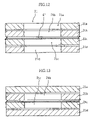
- FIG. 12 is a cross section of the portion shown in FIG. 11 ;
- FIG. 13 shows a modification of the structure shown in FIG. 12 ;
- FIG. 14 is another modification of the structure shown in FIG. 12 ;
- FIG. 15 is an exploded view of the structure of the fuse in FIG. 11 ;
- FIG. 16 is a perspective view of the structure of a conventional battery pack.
- FIG. 17 is a perspective view of a conventional fuse.
- FIG. 1 illustrates the main portion of a battery pack A that incorporates the printed wiring board 1 pertaining to a first embodiment of the present invention.
- the battery pack A is equipped with a chargeable battery 2 , which can be used, for instance, as a drive power source of a cellular telephone.
- the battery 2 is connected via two metal conductors 4 to a wiring pattern 12 (only partially depicted) formed on the wiring board 1 .
- the wiring board 1 includes a substrate 20 composed of an insulating material (such as glass epoxy), and on the back side thereof are formed four terminals 3 for receiving the supply of electricity from an external power source and charging the battery 2 .
- Four terminals 5 for supplying electricity from the battery 2 to the outside are provided on the top side of the wiring board 1 .
- a protection circuit 10 for preventing excess current from flowing into the battery 2 during charging is provided to the wiring board 1 .
- the protection circuit 10 consists of transistors or various other such electronic parts 11 .
- a fuse 6 is also provided to the wiring board 1 . As shown in FIG. 2 , two conductor pads 12 a and 12 b are formed as part of the wiring pattern 12 on the substrate 20 . The fuse 6 bridges these conductor pads 12 a and 12 b . The fuse 6 melts and breaks the circuit when current over the safe level flows through the wiring pattern 12 .
- the wiring pattern 12 can be formed, for example, by forming a thin film of copper on the substrate 20 , then removing the unnecessary portion by photolithography.
- the surface of the conductor pads 12 a and 12 b are plated with gold, for instance, after the formation of the wiring pattern 12 . This allows the fuse 6 to be connected well to the conductor pads 12 a and 12 b.
- the fuse 6 can be formed by bridging the conductor pads 12 a and 12 b with a wire W by wire bonding method. More specifically, the wire W (such as a solder wire) is first inserted into a capillary 80 , and the tip thereof is made to stick out from the capillary 80 . Next, the tip of the wire W is melted with a hydrogen flame or the like to form a ball 61 . The capillary 80 is then operated so that the ball 61 is press-bonded to the conductor pad 12 a . Preferably, the capillary 80 is subjected to high-frequency vibration at this point. This results in the wire W being more securely connected to the conductor pad 12 a.
- the wire W such as a solder wire
- the capillary 80 is then moved to where the other conductor pad 12 b is located.
- the wire W remains connected to the first conductor pad 12 a , and is played out from the tip of the capillary 80 according to the movement of the capillary 80 .
- the capillary 80 is then operated so that the wire W is press-bonded to the second conductor pad 12 b (preferably, the capillary 80 is subjected to high-frequency vibration at this point).
- the capillary 80 is moved laterally (to the right in FIG. 3 ) without playing out the wire W from the capillary 80 .
- the fuse 6 obtained in this manner may be covered with a potting material 7 for protection.
- the potting material 7 can be formed, for example, by dropping the liquefied glass epoxy resin from above the fuse 6 .
- the fuse 6 can be easily formed on the substrate 20 by a conventional wire bonding process. Therefore, no special mounting equipment is needed for the fuse 6 , which lowers the manufacturing cost and improves manufacturing efficiency.
- the fuse 6 consists of just a single piece of wire, and doesn't take up much space on the wiring board 1 .
- FIG. 4A it is also possible to provide the fuse 6 between two adjacent electronic parts 11 a and 11 b .
- the fuse 6 does not stick up above the tops of the electronic parts 11 a and 11 b . If [the fuse 6 ] is thus surrounded by the electronic parts 11 a and 11 b , the fuse 6 can be protected without providing the potting material 7 ( FIG. 2 ).
- FIG. 5 the main portions of a battery pack A 1 that incorporates the printed wiring board 1 ′ pertaining to a second embodiment of the present invention.
- the printed wiring board 1 ′ in FIG. 5 includes an insulating substrate 20 , over which four charging terminals 3 , a fuse 6 ′, electronic parts 11 , a wiring pattern 12 , and so forth are provided.
- the fuse 6 ′ is realized by making part of the wiring pattern 12 relatively narrow in width.
- the wiring pattern 12 including the fuse 6 ′ can be formed subjecting the conductor film formed on the substrate 20 to etching in a specific pattern by photolithography.
- a plurality of through holes 21 are formed in the substrate 20 in the vicinity of the fuse 6 ′.
- the illustrated through holes 21 (eight of them in FIG. 6 ) are divided into two equal groups, and sandwich the fuse 6 ′ on either side.
- the air inside the through holes 21 acts as a thermal insulator, making it less likely that joule heat generated by the fuse 6 ′ will be transmitted through the substrate 20 . Accordingly, the fuse 6 ′ will always be melted by the generated joule heat when excess current flows into the fuse 6 ′.
- the through holes 21 are formed by drilling, for example.
- the extent to which the joule heat generated by the fuse 6 ′ is diffused through the substrate 20 can be adjusted by varying the shape, size, and number of the through holes 21 .
- the fuse 6 ′ is exposed on the outside by providing an opening 31 in the resist layer 30 . This keeps the heat generated by the fuse 6 ′ from escaping through the resist layer 30 .
- FIGS. 9 and 10 illustrate the main parts of a printed wiring board 1 ′′ in a third embodiment of the present invention.
- the printed wiring board 1 ′′ includes first to third insulating substrates 20 a , 20 b , and 20 c .
- specific wiring patterns are formed on the upper and/or lower sides of the substrates 20 a to 20 c .
- the same fuse 6 ′ and through holes 21 as in the second embodiment are formed in the second substrate 20 b (see FIG. 6 ).
- nothing is provided corresponding to the resist layer 30 in FIG. 7 .
- a recess 40 facing the fuse 6 ′ is formed in the first substrate 20 a .
- joule heat generated by the fuse 6 ′ can be prevented from being directly transmitted to the first substrate 20 a .
- through holes may be formed in the first substrate 20 a instead of the recess 40 .
- FIGS. 11 and 12 illustrate a fuse 6 ′′ provided to a printed wiring board 1 ′′′ pertaining to a fourth embodiment of the present invention.
- the printed wiring board 1 ′′′ includes first to fourth substrates 21 a to 21 d , and a specific wiring pattern is formed on the upper and/or lower side of each of these substrates. These wiring patterns are electrically connected to each other via through holes provided in the substrates 21 a to 21 d (see 13 in FIG. 15 ).
- the fuse 6 ′′ is provided to the third substrate 21 c .
- the fuse 6 ′′ is exposed to the outside via through holes 71 consisting of openings 71 a to 71 d formed in the substrates 21 a to 21 d , respectively.
- the fuse 6 ′′ is provided as part of the wiring pattern formed on the third substrate 21 c , and bridges the opening 21 c .
- the fuse 6 ′′ can be formed by first forming the specific wiring pattern on the substrate 21 c , and then making the opening 21 c in the substrate 21 c .
- An etching technique that acts only on the substrate 21 c can be used to form this opening.
- openings 71 a to 71 d are provided to each of the respective substrates 21 a to 21 d in the embodiment illustrated in FIGS. 11 and 12 , but the present invention is not limited to this.
- openings 71 c and 71 d that communicate with each other can be provided to just the second and third substrates 21 b and 21 c .
- recesses 71 b ′ and 71 c ′ that communicate with each other may be provided to the second and third substrates 21 b and 21 c.
- the fuse 6 ′′ is formed as part of the wiring pattern in the embodiment illustrated in FIGS. 11 and 12 , but the present invention is not limited to this.
- a fuse 6 ′′′ readied separately from the 2p may be used.
- the opening 71 c can be formed by drilling or another such mechanical means.
- the fuse 6 ′′′ comprises two terminals 60 a ′′′ and a middle portion 12 b that extends between these terminals.
- the terminals 60 a ′′′ are electrically connected to the wiring pattern 12 on the second substrate 21 b via the through holes 13 .
Abstract
A printed wiring board includes a substrate (20) on which a wiring pattern (12) has been formed, and a fuse (6) provided on the substrate (20). One end of the fuse (6) is directly connected to a first pad (12 a) of the wiring pattern (12), and the other end of the fuse (6) is directly connected to a second pad (12 b) of the wiring pattern (12). The fuse (6) is covered by a protective material (7).
Description
This application is a division of application Ser. No. 10/221,616, filed Sep. 12, 2002 now abandoned, which application is incorporated herein by reference.
This invention relates to a printed wiring board equipped with a fuse.
Printed wiring boards equipped with fuses for circuit protection have been used in the past in a wide variety of electronic devices. FIG. 16 of this application illustrates a printed wiring board 101 used in a battery pack for a cellular telephone. This printed wiring board 101 is equipped with an insulating substrate 102, on which a specific wiring pattern (not shown) is formed. Also, a protection circuit 10 and a fuse 110 are mounted on this insulating substrate 102. The protection circuit 10 serves to prevent the overcharging of a battery 2, and consists of transistors or various other such electronic parts 11. The fuse 110 works as a failsafe device in the event that the protection circuit 10 should not function properly, and keeps excess current from flowing into the circuit.
The printed wiring board 101 is further provided with a charging terminal 3 for bringing electricity from a household outlet or the like to the battery 2. This electricity is supplied from a metal terminal 4, through the protection circuit 10 and the fuse 110, and to the battery 2.
As shown in FIG. 17 , the fuse 110 is equipped with a package 111 composed of an epoxy resin or the like, and leads 112 a and 112 b which protrude in opposite directions from this package 111. The package 111 is hollow, and an electroconductive material that will melt at a specific temperature is disposed on the inside thereof. The leads 112 a and 112 b are electrically connected to each other via this conductive member inside the package 111.
A problem encountered with the conventional printed wiring board 101 described above was that the size of the fuse 110 was different from that of the electronic parts 11. Consequently, some chip mounters for mounting the electronic parts 11 were unable to mount the fuse 110 on the insulating substrate 102, which meant that the fuse 110 had to be mounted manually, and this lowered the working efficiency. Furthermore, the fuse 110 tended to be bulky because it had the package 111. This hindered efforts at reducing the size of the printed wiring board 101.
The present invention has been conceived in light of the above situation, and it is an object thereof to provide a compact, fused printed wiring board by a simple and inexpensive means.
The printed wiring board provided by the present invention comprises an insulating substrate on which a wiring pattern has been formed, and a fuse including a circuit breaking means. The circuit breaking means is directly connected to the wiring pattern.
In a preferred embodiment of the present invention, the wiring pattern includes two conductor pads that are apart from each other, and the circuit breaking means bridges the two conductor pads.
Preferably, the circuit breaking means is covered with a protective material.
Preferably, the printed wiring board further comprises at least one electronic part mounted on the substrate, and the circuit breaking means is disposed lower than the electronic part.
Preferably, the circuit breaking means is a solder wire.
Preferably, the printed wiring board further comprises a heat insulating means disposed in the vicinity of the circuit breaking means.
In another preferred embodiment of the present invention, the circuit breaking means is formed integrally with the wiring pattern. In this case, the circuit breaking means is a relatively narrow portion of the wiring pattern, for example.
Preferably, the wiring pattern is composed of copper.
Preferably, the printed wiring board further comprises a resist layer that covers the wiring pattern, and the heat insulating means includes an opening formed in the resist layer.
Preferably, the heat insulating means is a through hole or a recess provided to the substrate. The circuit breaking means bridges the through hole or recess. Alternatively, the circuit breaking means may be provided inside the through hole.
In another preferred embodiment of the present invention, the printed wiring board further comprises an additional insulating substrate. The heat insulating means includes a through hole or recess formed in the additional insulating substrate.
Other features and advantages of the present invention should become clearer from the following detailed description through reference to the appended drawings.
Preferred embodiments of the present invention will now be described in specific terms through reference to the appended drawings.
A protection circuit 10 for preventing excess current from flowing into the battery 2 during charging is provided to the wiring board 1. The protection circuit 10 consists of transistors or various other such electronic parts 11. A fuse 6 is also provided to the wiring board 1. As shown in FIG. 2 , two conductor pads 12 a and 12 b are formed as part of the wiring pattern 12 on the substrate 20. The fuse 6 bridges these conductor pads 12 a and 12 b. The fuse 6 melts and breaks the circuit when current over the safe level flows through the wiring pattern 12.
The wiring pattern 12 can be formed, for example, by forming a thin film of copper on the substrate 20, then removing the unnecessary portion by photolithography. Preferably, the surface of the conductor pads 12 a and 12 b are plated with gold, for instance, after the formation of the wiring pattern 12. This allows the fuse 6 to be connected well to the conductor pads 12 a and 12 b.
As shown in FIG. 3 , the fuse 6 can be formed by bridging the conductor pads 12 a and 12 b with a wire W by wire bonding method. More specifically, the wire W (such as a solder wire) is first inserted into a capillary 80, and the tip thereof is made to stick out from the capillary 80. Next, the tip of the wire W is melted with a hydrogen flame or the like to form a ball 61. The capillary 80 is then operated so that the ball 61 is press-bonded to the conductor pad 12 a. Preferably, the capillary 80 is subjected to high-frequency vibration at this point. This results in the wire W being more securely connected to the conductor pad 12 a.
The capillary 80 is then moved to where the other conductor pad 12 b is located. The wire W remains connected to the first conductor pad 12 a, and is played out from the tip of the capillary 80 according to the movement of the capillary 80. The capillary 80 is then operated so that the wire W is press-bonded to the second conductor pad 12 b (preferably, the capillary 80 is subjected to high-frequency vibration at this point). Finally, the capillary 80 is moved laterally (to the right in FIG. 3 ) without playing out the wire W from the capillary 80. This breaks the wire W at the location of the second conductor pad 12 b, and the fuse 6 is obtained. As shown in FIG. 2 , the fuse 6 obtained in this manner may be covered with a potting material 7 for protection. The potting material 7 can be formed, for example, by dropping the liquefied glass epoxy resin from above the fuse 6.
With the first embodiment given above, the fuse 6 can be easily formed on the substrate 20 by a conventional wire bonding process. Therefore, no special mounting equipment is needed for the fuse 6, which lowers the manufacturing cost and improves manufacturing efficiency.
Also, the fuse 6 consists of just a single piece of wire, and doesn't take up much space on the wiring board 1. Thus, as shown in FIG. 4A , it is also possible to provide the fuse 6 between two adjacent electronic parts 11 a and 11 b. Preferably, as shown in FIG. 4B , the fuse 6 does not stick up above the tops of the electronic parts 11 a and 11 b. If [the fuse 6] is thus surrounded by the electronic parts 11 a and 11 b, the fuse 6 can be protected without providing the potting material 7 (FIG. 2 ).
As shown in FIG. 6 , the fuse 6′ is realized by making part of the wiring pattern 12 relatively narrow in width. The wiring pattern 12 including the fuse 6′ can be formed subjecting the conductor film formed on the substrate 20 to etching in a specific pattern by photolithography.
With the second embodiment of the present invention, a plurality of through holes 21 are formed in the substrate 20 in the vicinity of the fuse 6′. The illustrated through holes 21 (eight of them in FIG. 6 ) are divided into two equal groups, and sandwich the fuse 6′ on either side. With this configuration, the air inside the through holes 21 acts as a thermal insulator, making it less likely that joule heat generated by the fuse 6′ will be transmitted through the substrate 20. Accordingly, the fuse 6′ will always be melted by the generated joule heat when excess current flows into the fuse 6′. The through holes 21 are formed by drilling, for example. The extent to which the joule heat generated by the fuse 6′ is diffused through the substrate 20 can be adjusted by varying the shape, size, and number of the through holes 21.
After the formation of the wiring pattern 12, as shown in FIG. 7 , a resist layer 30 made of an epoxy or acrylic resin, for example, is formed on the substrate 20. This prevents the wiring pattern 12 from being corroded or damaged. Preferably, the fuse 6′ is exposed on the outside by providing an opening 31 in the resist layer 30. This keeps the heat generated by the fuse 6′ from escaping through the resist layer 30.
As shown well in FIG. 10 , a recess 40 facing the fuse 6′ is formed in the first substrate 20 a. With this configuration, joule heat generated by the fuse 6′ can be prevented from being directly transmitted to the first substrate 20 a. If an additional insulating substrate is provided over the first substrate 20 a, through holes may be formed in the first substrate 20 a instead of the recess 40.
As shown in FIG. 12 , the fuse 6″ is provided to the third substrate 21 c. The fuse 6″ is exposed to the outside via through holes 71 consisting of openings 71 a to 71 d formed in the substrates 21 a to 21 d, respectively.
The fuse 6″ is provided as part of the wiring pattern formed on the third substrate 21 c, and bridges the opening 21 c. The fuse 6″ can be formed by first forming the specific wiring pattern on the substrate 21 c, and then making the opening 21 c in the substrate 21 c. An etching technique that acts only on the substrate 21 c, for example, can be used to form this opening.
The openings 71 a to 71 d are provided to each of the respective substrates 21 a to 21 d in the embodiment illustrated in FIGS. 11 and 12 , but the present invention is not limited to this. For instance, as shown in FIG. 13 , openings 71 c and 71 d that communicate with each other can be provided to just the second and third substrates 21 b and 21 c. Alternatively, as shown in FIG. 14 , recesses 71 b′ and 71 c′ that communicate with each other may be provided to the second and third substrates 21 b and 21 c.
Also, the fuse 6″ is formed as part of the wiring pattern in the embodiment illustrated in FIGS. 11 and 12 , but the present invention is not limited to this. For instance, as shown in FIG. 15 , a fuse 6′″ readied separately from the 2p may be used. In this case, the opening 71 c can be formed by drilling or another such mechanical means. In the illustrated embodiment, the fuse 6′″ comprises two terminals 60 a′″ and a middle portion 12 b that extends between these terminals. The terminals 60 a′″ are electrically connected to the wiring pattern 12 on the second substrate 21 b via the through holes 13.
The present invention was described above, but it is obvious that this can be modified into other embodiments. These modifications are within the concept and scope of the present invention, and all changes that would be obvious to a person skilled in the art are encompassed in the claims given below.
Claims (4)
1. A printed wiring board comprising:
a first insulating substrate with a wiring pattern formed thereon;
a fuse including circuit breaking means formed integral with the wiring pattern; and
a second insulating substrate,
wherein the first insulating substrate is provided with two heat insulator groups arranged to sandwich the circuit breaking means, each of said heat insulator groups including a plurality of through holes formed in the first insulating substrate,
wherein the second insulating substrate is formed with a recess facing the circuit breaking means.
2. The board according to claim 1 , wherein the circuit breaking means is a relatively narrow portion of the wiring pattern.
3. The board according to claim 2 , wherein the wiring pattern is made of copper.
4. The board according to claim 1 , wherein the plurality of through holes is arranged in a row extending in parallel to the circuit breaking means.
Priority Applications (1)
| Application Number | Priority Date | Filing Date | Title |
|---|---|---|---|
| US11/062,297 US7116208B2 (en) | 2000-03-14 | 2005-02-17 | Printed-circuit board with fuse |
Applications Claiming Priority (9)
| Application Number | Priority Date | Filing Date | Title |
|---|---|---|---|
| JP2000070733 | 2000-03-14 | ||
| JP2000-70734 | 2000-03-14 | ||
| JP2000070734 | 2000-03-14 | ||
| JP2000-70733 | 2000-03-17 | ||
| JP2000-77641 | 2000-03-21 | ||
| JP2000077641 | 2000-03-21 | ||
| US10/221,616 US20030048620A1 (en) | 2000-03-14 | 2001-03-13 | Printed-circuit board with fuse |
| PCT/JP2001/001990 WO2001069988A1 (en) | 2000-03-14 | 2001-03-13 | Printed-circuit board with fuse |
| US11/062,297 US7116208B2 (en) | 2000-03-14 | 2005-02-17 | Printed-circuit board with fuse |
Related Parent Applications (3)
| Application Number | Title | Priority Date | Filing Date |
|---|---|---|---|
| US10/221,616 Division US20030048620A1 (en) | 2000-03-14 | 2001-03-13 | Printed-circuit board with fuse |
| PCT/JP2001/001990 Division WO2001069988A1 (en) | 2000-03-14 | 2001-03-13 | Printed-circuit board with fuse |
| US10221616 Division | 2001-03-13 |
Publications (2)
| Publication Number | Publication Date |
|---|---|
| US20050140490A1 US20050140490A1 (en) | 2005-06-30 |
| US7116208B2 true US7116208B2 (en) | 2006-10-03 |
Family
ID=27342663
Family Applications (2)
| Application Number | Title | Priority Date | Filing Date |
|---|---|---|---|
| US10/221,616 Abandoned US20030048620A1 (en) | 2000-03-14 | 2001-03-13 | Printed-circuit board with fuse |
| US11/062,297 Expired - Fee Related US7116208B2 (en) | 2000-03-14 | 2005-02-17 | Printed-circuit board with fuse |
Family Applications Before (1)
| Application Number | Title | Priority Date | Filing Date |
|---|---|---|---|
| US10/221,616 Abandoned US20030048620A1 (en) | 2000-03-14 | 2001-03-13 | Printed-circuit board with fuse |
Country Status (2)
| Country | Link |
|---|---|
| US (2) | US20030048620A1 (en) |
| WO (1) | WO2001069988A1 (en) |
Cited By (19)
| Publication number | Priority date | Publication date | Assignee | Title |
|---|---|---|---|---|
| US20060267722A1 (en) * | 2005-05-27 | 2006-11-30 | Alfons Graf | Electric Component with a Protected Current Feeding Terminal |
| US20070075822A1 (en) * | 2005-10-03 | 2007-04-05 | Littlefuse, Inc. | Fuse with cavity forming enclosure |
| US20070236849A1 (en) * | 2006-04-06 | 2007-10-11 | Littelfuse, Inc. | Leadless integrated circuit protection device |
| US20080100411A1 (en) * | 2006-10-31 | 2008-05-01 | Farshid Tofigh | Power controller with fusible link |
| US20080278276A1 (en) * | 2007-05-10 | 2008-11-13 | Banzo Juan I | System and method for interconnecting a plurality of printed circuits |
| US20080283289A1 (en) * | 2007-05-18 | 2008-11-20 | Fukui Precision Component (Shenzhen) Co., Ltd. | Printed circuit boards |
| US20100265031A1 (en) * | 2007-12-21 | 2010-10-21 | Chun-Chang Yen | Surface mount thin film fuse structure and method of manufacturing the same |
| US20110063070A1 (en) * | 2009-09-16 | 2011-03-17 | Littelfuse, Inc. | Metal film surface mount fuse |
| US20110210814A1 (en) * | 2008-11-25 | 2011-09-01 | Nanjing Sart Science & Technology Development Co., Ltd | Multi-layer blade fuse and the manufacturing method thereof |
| US20120013431A1 (en) * | 2010-07-16 | 2012-01-19 | Hans-Peter Blattler | Fuse element |
| US20120092123A1 (en) * | 2010-10-14 | 2012-04-19 | Avx Corporation | Low current fuse |
| US20120200974A1 (en) * | 2011-02-04 | 2012-08-09 | Murata Manufacturing Co., Ltd. | Electronic control device including interrupt wire |
| DE102010037390B4 (en) * | 2010-09-08 | 2012-08-30 | Vossloh-Schwabe Deutschland Gmbh | Multi-layer printed circuit board with printed circuit board fuse |
| US20130021131A1 (en) * | 2011-07-19 | 2013-01-24 | Whirlpool Corporation | Circuit board having arc tracking protection |
| US8421579B2 (en) * | 2010-10-12 | 2013-04-16 | Hung-Chih Chiu | Current protection device |
| TWI485738B (en) * | 2012-01-31 | 2015-05-21 | ||
| CN104779130A (en) * | 2014-01-10 | 2015-07-15 | 保险丝公司 | Ceramic chip fuse with offset fuse element |
| US20150371804A1 (en) * | 2014-06-19 | 2015-12-24 | Koa Corporation | Chip type fuse |
| US9425009B2 (en) | 2011-02-04 | 2016-08-23 | Denso Corporation | Electronic control device including interrupt wire |
Families Citing this family (31)
| Publication number | Priority date | Publication date | Assignee | Title |
|---|---|---|---|---|
| US7133266B1 (en) | 2000-11-21 | 2006-11-07 | Pass & Seymour, Inc. | Electrical wiring device |
| US7385475B2 (en) | 2002-01-10 | 2008-06-10 | Cooper Technologies Company | Low resistance polymer matrix fuse apparatus and method |
| US7436284B2 (en) | 2002-01-10 | 2008-10-14 | Cooper Technologies Company | Low resistance polymer matrix fuse apparatus and method |
| US7570148B2 (en) | 2002-01-10 | 2009-08-04 | Cooper Technologies Company | Low resistance polymer matrix fuse apparatus and method |
| DE10392979D2 (en) * | 2002-06-21 | 2005-07-14 | Continental Teves Ag & Co Ohg | Printed circuit board for electronic vehicle control units |
| EP1678988A1 (en) * | 2003-10-17 | 2006-07-12 | Koninklijke Philips Electronics N.V. | Printed circuit board including a fuse |
| US7239491B1 (en) | 2004-07-02 | 2007-07-03 | Pass & Seymore, Inc. | Protective device with miswire protection |
| US7295410B1 (en) | 2004-10-13 | 2007-11-13 | Pass & Seymour, Inc. | Protective device with miswire protection |
| DE102005002091A1 (en) * | 2005-01-14 | 2006-07-20 | Vishay Israel Ltd. | Fuse for an electronic circuit and method of making the fuse |
| US7238877B1 (en) * | 2006-02-22 | 2007-07-03 | Taylor-Listug, Inc. | Musical instrument string ground circuit breaker |
| EP2168410B1 (en) * | 2007-03-19 | 2018-05-16 | Conti Temic microelectronic GmbH | Electronic module comprising a conductor fuse |
| US20100164677A1 (en) * | 2008-12-29 | 2010-07-01 | Chin-Chi Yang | Fuse |
| DE102009040022B3 (en) * | 2009-09-03 | 2011-03-24 | Beru Ag | Method for forming a fuse and circuit board with fuse |
| CN103329407B (en) * | 2011-01-21 | 2016-08-10 | 博泽沃尔兹堡汽车零部件有限公司 | The control electronic device of protection device, particularly motor vehicle component |
| JP5583042B2 (en) * | 2011-02-04 | 2014-09-03 | 株式会社デンソー | Electronic control unit |
| JP5333475B2 (en) * | 2011-02-04 | 2013-11-06 | 株式会社デンソー | Electronic control unit |
| JP5494517B2 (en) * | 2011-02-04 | 2014-05-14 | 株式会社デンソー | Electronic control unit |
| JP5333474B2 (en) * | 2011-02-04 | 2013-11-06 | 株式会社デンソー | Electronic control unit |
| JP2012164756A (en) * | 2011-02-04 | 2012-08-30 | Denso Corp | Electronic control device |
| US8780518B2 (en) | 2011-02-04 | 2014-07-15 | Denso Corporation | Electronic control device including interrupt wire |
| JP5333473B2 (en) * | 2011-02-04 | 2013-11-06 | 株式会社デンソー | Electronic control unit |
| JP5333476B2 (en) * | 2011-02-04 | 2013-11-06 | 株式会社デンソー | Electronic control unit |
| US20130314201A1 (en) * | 2012-05-23 | 2013-11-28 | Tzye Perng Poh | Over-current protection fuses |
| JP5561382B2 (en) * | 2013-01-09 | 2014-07-30 | 株式会社デンソー | Electronic control unit |
| JP5626377B2 (en) * | 2013-01-10 | 2014-11-19 | 株式会社デンソー | Electronic control unit |
| JP2013084987A (en) * | 2013-01-10 | 2013-05-09 | Denso Corp | Manufacturing method of wiring board |
| JP6453720B2 (en) * | 2015-06-24 | 2019-01-16 | 住友電気工業株式会社 | Flexible printed wiring board |
| CN106710995B (en) * | 2017-01-20 | 2019-09-17 | 东莞市博钺电子有限公司 | Chip fuse |
| FR3067871A1 (en) * | 2017-06-19 | 2018-12-21 | Zodiac Aero Electric | PROTECTIVE DEVICE FOR AN ELECTRICAL DISTRIBUTION SYSTEM OF AN AIRCRAFT ELECTRICAL SYSTEM |
| KR102482155B1 (en) * | 2017-10-17 | 2022-12-29 | 에이치엘만도 주식회사 | Fuse pad, printed circuit board including the fuse pad and method for manufacturing thereof |
| US11729906B2 (en) * | 2018-12-12 | 2023-08-15 | Eaton Intelligent Power Limited | Printed circuit board with integrated fusing and arc suppression |
Citations (32)
| Publication number | Priority date | Publication date | Assignee | Title |
|---|---|---|---|---|
| US2934627A (en) * | 1957-04-09 | 1960-04-26 | Northrop Corp | Electric printed circuit component |
| US3334205A (en) * | 1966-06-23 | 1967-08-01 | Quantic Ind Inc | Micro-circuit bridge and method |
| US3358363A (en) | 1963-07-19 | 1967-12-19 | English Electric Co Ltd | Method of making fuse elements |
| US3585556A (en) | 1969-07-22 | 1971-06-15 | Ashok R Hingorany | Electrical fuse and heater units |
| JPS5147864A (en) | 1974-10-18 | 1976-04-23 | Yoshida Kogyo Kk | Isuno shiitojitoritsuke hoho |
| JPS53109058A (en) | 1977-03-04 | 1978-09-22 | Glaenzer Spicer Sa | Rotary coupling |
| JPS5571574A (en) | 1978-11-24 | 1980-05-29 | Matsushita Electric Ind Co Ltd | Image recorder |
| JPS55108777A (en) | 1979-02-14 | 1980-08-21 | Hitachi Ltd | Light receiving element |
| US4296398A (en) | 1978-12-18 | 1981-10-20 | Mcgalliard James D | Printed circuit fuse assembly |
| US4379318A (en) | 1979-09-21 | 1983-04-05 | Nissan Motor Company, Limited | Overcurrent safety construction for a printed circuit board |
| US4394639A (en) * | 1978-12-18 | 1983-07-19 | Mcgalliard James D | Printed circuit fuse assembly |
| JPS58182343A (en) | 1982-04-19 | 1983-10-25 | Nippon Telegr & Teleph Corp <Ntt> | Informing system of network information |
| US4626818A (en) | 1983-11-28 | 1986-12-02 | Centralab, Inc. | Device for programmable thick film networks |
| US4652848A (en) | 1986-06-06 | 1987-03-24 | Northern Telecom Limited | Fusible link |
| US4873506A (en) * | 1988-03-09 | 1989-10-10 | Cooper Industries, Inc. | Metallo-organic film fractional ampere fuses and method of making |
| JPH02281649A (en) | 1989-04-21 | 1990-11-19 | Mitsubishi Electric Corp | Hybrid integrated circuit |
| US5097246A (en) * | 1990-04-16 | 1992-03-17 | Cooper Industries, Inc. | Low amperage microfuse |
| US5097247A (en) | 1991-06-03 | 1992-03-17 | North American Philips Corporation | Heat actuated fuse apparatus with solder link |
| US5099219A (en) | 1991-02-28 | 1992-03-24 | Rock, Ltd. Partnership | Fusible flexible printed circuit and method of making same |
| US5130689A (en) | 1989-05-09 | 1992-07-14 | Leach & Garner Co. | Intermetallic time-temperature integration fuse |
| JPH05120985A (en) | 1991-10-30 | 1993-05-18 | Rohm Co Ltd | Fuse |
| JPH05258653A (en) | 1992-03-12 | 1993-10-08 | Uchihashi Estec Co Ltd | Substrate type temperature fuse |
| JPH0669626A (en) | 1992-08-12 | 1994-03-11 | Sony Corp | Mounting structure for circuit protecting element |
| US5309625A (en) * | 1992-07-16 | 1994-05-10 | Sumitomo Wiring Systems, Ltd. | Card type fuse and method of producing the same |
| US5543774A (en) | 1993-05-28 | 1996-08-06 | Telefonaktiebolaget Ericsson | Method and a device for protecting a printed circuit board against overcurrents |
| US5644281A (en) | 1992-04-07 | 1997-07-01 | Rohm Co., Ltd. | Electronic component incorporating solder fuse wire |
| US5682057A (en) | 1995-03-03 | 1997-10-28 | Rohm Co. Ltd. | Semiconductor device incorporating a temperature fuse |
| US5777540A (en) | 1996-01-29 | 1998-07-07 | Cts Corporation | Encapsulated fuse having a conductive polymer and non-cured deoxidant |
| US5914649A (en) * | 1997-03-28 | 1999-06-22 | Hitachi Chemical Company, Ltd. | Chip fuse and process for production thereof |
| US5923239A (en) * | 1997-12-02 | 1999-07-13 | Littelfuse, Inc. | Printed circuit board assembly having an integrated fusible link |
| JP2000311959A (en) | 1999-04-27 | 2000-11-07 | Sanyo Electric Co Ltd | Semiconductor device and manufacture of the same |
| US6384708B1 (en) * | 1997-09-04 | 2002-05-07 | Wickmann-Werke Gmbh | Electrical fuse element |
Family Cites Families (6)
| Publication number | Priority date | Publication date | Assignee | Title |
|---|---|---|---|---|
| JPS5147864U (en) * | 1974-10-08 | 1976-04-09 | ||
| JPS53109058U (en) * | 1977-02-08 | 1978-09-01 | ||
| JPS5742183Y2 (en) * | 1978-11-09 | 1982-09-17 | ||
| JPS55108777U (en) * | 1979-01-24 | 1980-07-30 | ||
| JPS58182343U (en) * | 1982-05-31 | 1983-12-05 | カルソニックカンセイ株式会社 | printed circuit board equipment |
| JPH0669629A (en) * | 1992-08-21 | 1994-03-11 | Matsushita Electric Ind Co Ltd | Scriber for ceramic board or other circuit board |
-
2001
- 2001-03-13 WO PCT/JP2001/001990 patent/WO2001069988A1/en active Application Filing
- 2001-03-13 US US10/221,616 patent/US20030048620A1/en not_active Abandoned
-
2005
- 2005-02-17 US US11/062,297 patent/US7116208B2/en not_active Expired - Fee Related
Patent Citations (32)
| Publication number | Priority date | Publication date | Assignee | Title |
|---|---|---|---|---|
| US2934627A (en) * | 1957-04-09 | 1960-04-26 | Northrop Corp | Electric printed circuit component |
| US3358363A (en) | 1963-07-19 | 1967-12-19 | English Electric Co Ltd | Method of making fuse elements |
| US3334205A (en) * | 1966-06-23 | 1967-08-01 | Quantic Ind Inc | Micro-circuit bridge and method |
| US3585556A (en) | 1969-07-22 | 1971-06-15 | Ashok R Hingorany | Electrical fuse and heater units |
| JPS5147864A (en) | 1974-10-18 | 1976-04-23 | Yoshida Kogyo Kk | Isuno shiitojitoritsuke hoho |
| JPS53109058A (en) | 1977-03-04 | 1978-09-22 | Glaenzer Spicer Sa | Rotary coupling |
| JPS5571574A (en) | 1978-11-24 | 1980-05-29 | Matsushita Electric Ind Co Ltd | Image recorder |
| US4296398A (en) | 1978-12-18 | 1981-10-20 | Mcgalliard James D | Printed circuit fuse assembly |
| US4394639A (en) * | 1978-12-18 | 1983-07-19 | Mcgalliard James D | Printed circuit fuse assembly |
| JPS55108777A (en) | 1979-02-14 | 1980-08-21 | Hitachi Ltd | Light receiving element |
| US4379318A (en) | 1979-09-21 | 1983-04-05 | Nissan Motor Company, Limited | Overcurrent safety construction for a printed circuit board |
| JPS58182343A (en) | 1982-04-19 | 1983-10-25 | Nippon Telegr & Teleph Corp <Ntt> | Informing system of network information |
| US4626818A (en) | 1983-11-28 | 1986-12-02 | Centralab, Inc. | Device for programmable thick film networks |
| US4652848A (en) | 1986-06-06 | 1987-03-24 | Northern Telecom Limited | Fusible link |
| US4873506A (en) * | 1988-03-09 | 1989-10-10 | Cooper Industries, Inc. | Metallo-organic film fractional ampere fuses and method of making |
| JPH02281649A (en) | 1989-04-21 | 1990-11-19 | Mitsubishi Electric Corp | Hybrid integrated circuit |
| US5130689A (en) | 1989-05-09 | 1992-07-14 | Leach & Garner Co. | Intermetallic time-temperature integration fuse |
| US5097246A (en) * | 1990-04-16 | 1992-03-17 | Cooper Industries, Inc. | Low amperage microfuse |
| US5099219A (en) | 1991-02-28 | 1992-03-24 | Rock, Ltd. Partnership | Fusible flexible printed circuit and method of making same |
| US5097247A (en) | 1991-06-03 | 1992-03-17 | North American Philips Corporation | Heat actuated fuse apparatus with solder link |
| JPH05120985A (en) | 1991-10-30 | 1993-05-18 | Rohm Co Ltd | Fuse |
| JPH05258653A (en) | 1992-03-12 | 1993-10-08 | Uchihashi Estec Co Ltd | Substrate type temperature fuse |
| US5644281A (en) | 1992-04-07 | 1997-07-01 | Rohm Co., Ltd. | Electronic component incorporating solder fuse wire |
| US5309625A (en) * | 1992-07-16 | 1994-05-10 | Sumitomo Wiring Systems, Ltd. | Card type fuse and method of producing the same |
| JPH0669626A (en) | 1992-08-12 | 1994-03-11 | Sony Corp | Mounting structure for circuit protecting element |
| US5543774A (en) | 1993-05-28 | 1996-08-06 | Telefonaktiebolaget Ericsson | Method and a device for protecting a printed circuit board against overcurrents |
| US5682057A (en) | 1995-03-03 | 1997-10-28 | Rohm Co. Ltd. | Semiconductor device incorporating a temperature fuse |
| US5777540A (en) | 1996-01-29 | 1998-07-07 | Cts Corporation | Encapsulated fuse having a conductive polymer and non-cured deoxidant |
| US5914649A (en) * | 1997-03-28 | 1999-06-22 | Hitachi Chemical Company, Ltd. | Chip fuse and process for production thereof |
| US6384708B1 (en) * | 1997-09-04 | 2002-05-07 | Wickmann-Werke Gmbh | Electrical fuse element |
| US5923239A (en) * | 1997-12-02 | 1999-07-13 | Littelfuse, Inc. | Printed circuit board assembly having an integrated fusible link |
| JP2000311959A (en) | 1999-04-27 | 2000-11-07 | Sanyo Electric Co Ltd | Semiconductor device and manufacture of the same |
Cited By (33)
| Publication number | Priority date | Publication date | Assignee | Title |
|---|---|---|---|---|
| US7504925B2 (en) * | 2005-05-27 | 2009-03-17 | Infineon Technologies Ag | Electric component with a protected current feeding terminal |
| US20060267722A1 (en) * | 2005-05-27 | 2006-11-30 | Alfons Graf | Electric Component with a Protected Current Feeding Terminal |
| US20070075822A1 (en) * | 2005-10-03 | 2007-04-05 | Littlefuse, Inc. | Fuse with cavity forming enclosure |
| US20090102595A1 (en) * | 2005-10-03 | 2009-04-23 | Littlefuse, Inc. | Fuse with cavity forming enclosure |
| US20070236849A1 (en) * | 2006-04-06 | 2007-10-11 | Littelfuse, Inc. | Leadless integrated circuit protection device |
| US20080100411A1 (en) * | 2006-10-31 | 2008-05-01 | Farshid Tofigh | Power controller with fusible link |
| US7760482B2 (en) * | 2006-10-31 | 2010-07-20 | Leach International Corporation | Power controller with fusible link |
| US20080278276A1 (en) * | 2007-05-10 | 2008-11-13 | Banzo Juan I | System and method for interconnecting a plurality of printed circuits |
| US7701321B2 (en) | 2007-05-10 | 2010-04-20 | Delphi Technologies, Inc. | System and method for interconnecting a plurality of printed circuits |
| US8049113B2 (en) * | 2007-05-18 | 2011-11-01 | Fukui Precision Component (Shenzhen) Co., Ltd. | Printed circuit boards |
| US20080283289A1 (en) * | 2007-05-18 | 2008-11-20 | Fukui Precision Component (Shenzhen) Co., Ltd. | Printed circuit boards |
| US20100265031A1 (en) * | 2007-12-21 | 2010-10-21 | Chun-Chang Yen | Surface mount thin film fuse structure and method of manufacturing the same |
| US20110210814A1 (en) * | 2008-11-25 | 2011-09-01 | Nanjing Sart Science & Technology Development Co., Ltd | Multi-layer blade fuse and the manufacturing method thereof |
| US8957755B2 (en) * | 2008-11-25 | 2015-02-17 | Nanjing Sart Science & Technology Development Co., Ltd. | Multi-layer blade fuse and the manufacturing method thereof |
| US20110063070A1 (en) * | 2009-09-16 | 2011-03-17 | Littelfuse, Inc. | Metal film surface mount fuse |
| US8659384B2 (en) * | 2009-09-16 | 2014-02-25 | Littelfuse, Inc. | Metal film surface mount fuse |
| US20120013431A1 (en) * | 2010-07-16 | 2012-01-19 | Hans-Peter Blattler | Fuse element |
| US10755884B2 (en) * | 2010-07-16 | 2020-08-25 | Schurter Ag | Fuse element |
| DE102010037390B4 (en) * | 2010-09-08 | 2012-08-30 | Vossloh-Schwabe Deutschland Gmbh | Multi-layer printed circuit board with printed circuit board fuse |
| US8421579B2 (en) * | 2010-10-12 | 2013-04-16 | Hung-Chih Chiu | Current protection device |
| US20120092123A1 (en) * | 2010-10-14 | 2012-04-19 | Avx Corporation | Low current fuse |
| US9847203B2 (en) * | 2010-10-14 | 2017-12-19 | Avx Corporation | Low current fuse |
| US20120200974A1 (en) * | 2011-02-04 | 2012-08-09 | Murata Manufacturing Co., Ltd. | Electronic control device including interrupt wire |
| US9166397B2 (en) | 2011-02-04 | 2015-10-20 | Denso Corporation | Electronic control device including interrupt wire |
| US9425009B2 (en) | 2011-02-04 | 2016-08-23 | Denso Corporation | Electronic control device including interrupt wire |
| US8971006B2 (en) * | 2011-02-04 | 2015-03-03 | Denso Corporation | Electronic control device including interrupt wire |
| US10064266B2 (en) * | 2011-07-19 | 2018-08-28 | Whirlpool Corporation | Circuit board having arc tracking protection |
| US20130021131A1 (en) * | 2011-07-19 | 2013-01-24 | Whirlpool Corporation | Circuit board having arc tracking protection |
| TWI485738B (en) * | 2012-01-31 | 2015-05-21 | ||
| CN104779130A (en) * | 2014-01-10 | 2015-07-15 | 保险丝公司 | Ceramic chip fuse with offset fuse element |
| US20150200067A1 (en) * | 2014-01-10 | 2015-07-16 | Littelfuse, Inc. | Ceramic chip fuse with offset fuse element |
| US20150371804A1 (en) * | 2014-06-19 | 2015-12-24 | Koa Corporation | Chip type fuse |
| US9779904B2 (en) * | 2014-06-19 | 2017-10-03 | Koa Corporation | Chip type fuse |
Also Published As
| Publication number | Publication date |
|---|---|
| US20050140490A1 (en) | 2005-06-30 |
| WO2001069988A1 (en) | 2001-09-20 |
| US20030048620A1 (en) | 2003-03-13 |
Similar Documents
| Publication | Publication Date | Title |
|---|---|---|
| US7116208B2 (en) | Printed-circuit board with fuse | |
| KR850000216Y1 (en) | Printed circuit board | |
| KR100426825B1 (en) | Semiconductor device | |
| KR100191186B1 (en) | Current protecting element | |
| US5764485A (en) | Multi-layer PCB blockade-via pad-connection | |
| KR100367126B1 (en) | Through hole bump contact | |
| US6054759A (en) | Semiconductor chip and package with heat dissipation | |
| KR960019670A (en) | Semiconductor chip package and manufacturing method thereof | |
| US20090126980A1 (en) | Printed wiring board | |
| TW200929310A (en) | Surface Mounted Technology type thin film fuse structure and the manufacturing method thereof | |
| US5892657A (en) | Electronic-circuit assembly and its manufacturing method | |
| JP2008153657A (en) | Power semiconductor module having contact spring | |
| CN101471208B (en) | Manufacturing method of surface bonding type film fuse | |
| CN100581326C (en) | Multilayer printed wiring board and method for manufacturing same | |
| US6570271B2 (en) | Apparatus for routing signals | |
| JPH02301182A (en) | Printed circuit board for flat mounting structure | |
| US6380059B1 (en) | Method of breaking electrically conductive traces on substrate into open-circuited state | |
| JPH08153456A (en) | Current protecting element | |
| EP0171783A2 (en) | Module board and module using the same and method of treating them | |
| CN201130650Y (en) | Surface-contact type thin film safety wire structure | |
| US20040055782A1 (en) | Surface-mounting type electronic circuit unit having no melting of solder attaching electric part thereto | |
| US20040119155A1 (en) | Metal wiring board and method for manufacturing the same | |
| JP3593249B2 (en) | Conversion module | |
| JPH07221419A (en) | Hybrid integrated circuit device | |
| KR100485872B1 (en) | Printed Circuit Board and Manufacturing Method of Jumper therefor |
Legal Events
| Date | Code | Title | Description |
|---|---|---|---|
| FPAY | Fee payment |
Year of fee payment: 4 |
|
| FPAY | Fee payment |
Year of fee payment: 8 |
|
| FEPP | Fee payment procedure |
Free format text: MAINTENANCE FEE REMINDER MAILED (ORIGINAL EVENT CODE: REM.) |
|
| LAPS | Lapse for failure to pay maintenance fees |
Free format text: PATENT EXPIRED FOR FAILURE TO PAY MAINTENANCE FEES (ORIGINAL EVENT CODE: EXP.); ENTITY STATUS OF PATENT OWNER: LARGE ENTITY |
|
| STCH | Information on status: patent discontinuation |
Free format text: PATENT EXPIRED DUE TO NONPAYMENT OF MAINTENANCE FEES UNDER 37 CFR 1.362 |