US7125789B2 - Composite metal column for mounting semiconductor device - Google Patents
Composite metal column for mounting semiconductor device Download PDFInfo
- Publication number
- US7125789B2 US7125789B2 US10/732,666 US73266603A US7125789B2 US 7125789 B2 US7125789 B2 US 7125789B2 US 73266603 A US73266603 A US 73266603A US 7125789 B2 US7125789 B2 US 7125789B2
- Authority
- US
- United States
- Prior art keywords
- sheet
- members
- die
- pads
- solder
- Prior art date
- Legal status (The legal status is an assumption and is not a legal conclusion. Google has not performed a legal analysis and makes no representation as to the accuracy of the status listed.)
- Active, expires
Links
Images


Classifications
-
- H—ELECTRICITY
- H05—ELECTRIC TECHNIQUES NOT OTHERWISE PROVIDED FOR
- H05K—PRINTED CIRCUITS; CASINGS OR CONSTRUCTIONAL DETAILS OF ELECTRIC APPARATUS; MANUFACTURE OF ASSEMBLAGES OF ELECTRICAL COMPONENTS
- H05K3/00—Apparatus or processes for manufacturing printed circuits
- H05K3/30—Assembling printed circuits with electric components, e.g. with resistor
- H05K3/32—Assembling printed circuits with electric components, e.g. with resistor electrically connecting electric components or wires to printed circuits
- H05K3/34—Assembling printed circuits with electric components, e.g. with resistor electrically connecting electric components or wires to printed circuits by soldering
- H05K3/341—Surface mounted components
- H05K3/3431—Leadless components
- H05K3/3436—Leadless components having an array of bottom contacts, e.g. pad grid array or ball grid array components
-
- B—PERFORMING OPERATIONS; TRANSPORTING
- B23—MACHINE TOOLS; METAL-WORKING NOT OTHERWISE PROVIDED FOR
- B23K—SOLDERING OR UNSOLDERING; WELDING; CLADDING OR PLATING BY SOLDERING OR WELDING; CUTTING BY APPLYING HEAT LOCALLY, e.g. FLAME CUTTING; WORKING BY LASER BEAM
- B23K3/00—Tools, devices, or special appurtenances for soldering, e.g. brazing, or unsoldering, not specially adapted for particular methods
- B23K3/06—Solder feeding devices; Solder melting pans
- B23K3/0607—Solder feeding devices
- B23K3/0623—Solder feeding devices for shaped solder piece feeding, e.g. preforms, bumps, balls, pellets, droplets
-
- H—ELECTRICITY
- H01—ELECTRIC ELEMENTS
- H01L—SEMICONDUCTOR DEVICES NOT COVERED BY CLASS H10
- H01L21/00—Processes or apparatus adapted for the manufacture or treatment of semiconductor or solid state devices or of parts thereof
- H01L21/02—Manufacture or treatment of semiconductor devices or of parts thereof
- H01L21/04—Manufacture or treatment of semiconductor devices or of parts thereof the devices having at least one potential-jump barrier or surface barrier, e.g. PN junction, depletion layer or carrier concentration layer
- H01L21/50—Assembly of semiconductor devices using processes or apparatus not provided for in a single one of the subgroups H01L21/06 - H01L21/326, e.g. sealing of a cap to a base of a container
- H01L21/60—Attaching or detaching leads or other conductive members, to be used for carrying current to or from the device in operation
-
- H—ELECTRICITY
- H01—ELECTRIC ELEMENTS
- H01L—SEMICONDUCTOR DEVICES NOT COVERED BY CLASS H10
- H01L24/00—Arrangements for connecting or disconnecting semiconductor or solid-state bodies; Methods or apparatus related thereto
- H01L24/01—Means for bonding being attached to, or being formed on, the surface to be connected, e.g. chip-to-package, die-attach, "first-level" interconnects; Manufacturing methods related thereto
- H01L24/10—Bump connectors ; Manufacturing methods related thereto
- H01L24/11—Manufacturing methods
-
- H—ELECTRICITY
- H01—ELECTRIC ELEMENTS
- H01L—SEMICONDUCTOR DEVICES NOT COVERED BY CLASS H10
- H01L24/00—Arrangements for connecting or disconnecting semiconductor or solid-state bodies; Methods or apparatus related thereto
- H01L24/01—Means for bonding being attached to, or being formed on, the surface to be connected, e.g. chip-to-package, die-attach, "first-level" interconnects; Manufacturing methods related thereto
- H01L24/10—Bump connectors ; Manufacturing methods related thereto
- H01L24/12—Structure, shape, material or disposition of the bump connectors prior to the connecting process
- H01L24/13—Structure, shape, material or disposition of the bump connectors prior to the connecting process of an individual bump connector
-
- B—PERFORMING OPERATIONS; TRANSPORTING
- B23—MACHINE TOOLS; METAL-WORKING NOT OTHERWISE PROVIDED FOR
- B23K—SOLDERING OR UNSOLDERING; WELDING; CLADDING OR PLATING BY SOLDERING OR WELDING; CUTTING BY APPLYING HEAT LOCALLY, e.g. FLAME CUTTING; WORKING BY LASER BEAM
- B23K2101/00—Articles made by soldering, welding or cutting
- B23K2101/36—Electric or electronic devices
- B23K2101/40—Semiconductor devices
-
- B—PERFORMING OPERATIONS; TRANSPORTING
- B23—MACHINE TOOLS; METAL-WORKING NOT OTHERWISE PROVIDED FOR
- B23K—SOLDERING OR UNSOLDERING; WELDING; CLADDING OR PLATING BY SOLDERING OR WELDING; CUTTING BY APPLYING HEAT LOCALLY, e.g. FLAME CUTTING; WORKING BY LASER BEAM
- B23K35/00—Rods, electrodes, materials, or media, for use in soldering, welding, or cutting
- B23K35/001—Interlayers, transition pieces for metallurgical bonding of workpieces
-
- B—PERFORMING OPERATIONS; TRANSPORTING
- B23—MACHINE TOOLS; METAL-WORKING NOT OTHERWISE PROVIDED FOR
- B23K—SOLDERING OR UNSOLDERING; WELDING; CLADDING OR PLATING BY SOLDERING OR WELDING; CUTTING BY APPLYING HEAT LOCALLY, e.g. FLAME CUTTING; WORKING BY LASER BEAM
- B23K35/00—Rods, electrodes, materials, or media, for use in soldering, welding, or cutting
- B23K35/02—Rods, electrodes, materials, or media, for use in soldering, welding, or cutting characterised by mechanical features, e.g. shape
- B23K35/0222—Rods, electrodes, materials, or media, for use in soldering, welding, or cutting characterised by mechanical features, e.g. shape for use in soldering, brazing
- B23K35/0233—Sheets, foils
- B23K35/0238—Sheets, foils layered
-
- H—ELECTRICITY
- H01—ELECTRIC ELEMENTS
- H01L—SEMICONDUCTOR DEVICES NOT COVERED BY CLASS H10
- H01L2224/00—Indexing scheme for arrangements for connecting or disconnecting semiconductor or solid-state bodies and methods related thereto as covered by H01L24/00
- H01L2224/01—Means for bonding being attached to, or being formed on, the surface to be connected, e.g. chip-to-package, die-attach, "first-level" interconnects; Manufacturing methods related thereto
- H01L2224/10—Bump connectors; Manufacturing methods related thereto
- H01L2224/12—Structure, shape, material or disposition of the bump connectors prior to the connecting process
- H01L2224/13—Structure, shape, material or disposition of the bump connectors prior to the connecting process of an individual bump connector
- H01L2224/13001—Core members of the bump connector
- H01L2224/13099—Material
- H01L2224/131—Material with a principal constituent of the material being a metal or a metalloid, e.g. boron [B], silicon [Si], germanium [Ge], arsenic [As], antimony [Sb], tellurium [Te] and polonium [Po], and alloys thereof
-
- H—ELECTRICITY
- H01—ELECTRIC ELEMENTS
- H01L—SEMICONDUCTOR DEVICES NOT COVERED BY CLASS H10
- H01L2224/00—Indexing scheme for arrangements for connecting or disconnecting semiconductor or solid-state bodies and methods related thereto as covered by H01L24/00
- H01L2224/01—Means for bonding being attached to, or being formed on, the surface to be connected, e.g. chip-to-package, die-attach, "first-level" interconnects; Manufacturing methods related thereto
- H01L2224/26—Layer connectors, e.g. plate connectors, solder or adhesive layers; Manufacturing methods related thereto
- H01L2224/28—Structure, shape, material or disposition of the layer connectors prior to the connecting process
- H01L2224/29—Structure, shape, material or disposition of the layer connectors prior to the connecting process of an individual layer connector
- H01L2224/29001—Core members of the layer connector
- H01L2224/29099—Material
- H01L2224/291—Material with a principal constituent of the material being a metal or a metalloid, e.g. boron [B], silicon [Si], germanium [Ge], arsenic [As], antimony [Sb], tellurium [Te] and polonium [Po], and alloys thereof
- H01L2224/29101—Material with a principal constituent of the material being a metal or a metalloid, e.g. boron [B], silicon [Si], germanium [Ge], arsenic [As], antimony [Sb], tellurium [Te] and polonium [Po], and alloys thereof the principal constituent melting at a temperature of less than 400°C
- H01L2224/29109—Indium [In] as principal constituent
-
- H—ELECTRICITY
- H01—ELECTRIC ELEMENTS
- H01L—SEMICONDUCTOR DEVICES NOT COVERED BY CLASS H10
- H01L2224/00—Indexing scheme for arrangements for connecting or disconnecting semiconductor or solid-state bodies and methods related thereto as covered by H01L24/00
- H01L2224/01—Means for bonding being attached to, or being formed on, the surface to be connected, e.g. chip-to-package, die-attach, "first-level" interconnects; Manufacturing methods related thereto
- H01L2224/26—Layer connectors, e.g. plate connectors, solder or adhesive layers; Manufacturing methods related thereto
- H01L2224/28—Structure, shape, material or disposition of the layer connectors prior to the connecting process
- H01L2224/29—Structure, shape, material or disposition of the layer connectors prior to the connecting process of an individual layer connector
- H01L2224/29001—Core members of the layer connector
- H01L2224/29099—Material
- H01L2224/291—Material with a principal constituent of the material being a metal or a metalloid, e.g. boron [B], silicon [Si], germanium [Ge], arsenic [As], antimony [Sb], tellurium [Te] and polonium [Po], and alloys thereof
- H01L2224/29101—Material with a principal constituent of the material being a metal or a metalloid, e.g. boron [B], silicon [Si], germanium [Ge], arsenic [As], antimony [Sb], tellurium [Te] and polonium [Po], and alloys thereof the principal constituent melting at a temperature of less than 400°C
- H01L2224/29111—Tin [Sn] as principal constituent
-
- H—ELECTRICITY
- H01—ELECTRIC ELEMENTS
- H01L—SEMICONDUCTOR DEVICES NOT COVERED BY CLASS H10
- H01L2224/00—Indexing scheme for arrangements for connecting or disconnecting semiconductor or solid-state bodies and methods related thereto as covered by H01L24/00
- H01L2224/80—Methods for connecting semiconductor or other solid state bodies using means for bonding being attached to, or being formed on, the surface to be connected
- H01L2224/81—Methods for connecting semiconductor or other solid state bodies using means for bonding being attached to, or being formed on, the surface to be connected using a bump connector
- H01L2224/818—Bonding techniques
- H01L2224/81801—Soldering or alloying
-
- H—ELECTRICITY
- H01—ELECTRIC ELEMENTS
- H01L—SEMICONDUCTOR DEVICES NOT COVERED BY CLASS H10
- H01L23/00—Details of semiconductor or other solid state devices
- H01L23/562—Protection against mechanical damage
-
- H—ELECTRICITY
- H01—ELECTRIC ELEMENTS
- H01L—SEMICONDUCTOR DEVICES NOT COVERED BY CLASS H10
- H01L24/00—Arrangements for connecting or disconnecting semiconductor or solid-state bodies; Methods or apparatus related thereto
- H01L24/80—Methods for connecting semiconductor or other solid state bodies using means for bonding being attached to, or being formed on, the surface to be connected
- H01L24/81—Methods for connecting semiconductor or other solid state bodies using means for bonding being attached to, or being formed on, the surface to be connected using a bump connector
-
- H—ELECTRICITY
- H01—ELECTRIC ELEMENTS
- H01L—SEMICONDUCTOR DEVICES NOT COVERED BY CLASS H10
- H01L2924/00—Indexing scheme for arrangements or methods for connecting or disconnecting semiconductor or solid-state bodies as covered by H01L24/00
- H01L2924/0001—Technical content checked by a classifier
- H01L2924/00013—Fully indexed content
-
- H—ELECTRICITY
- H01—ELECTRIC ELEMENTS
- H01L—SEMICONDUCTOR DEVICES NOT COVERED BY CLASS H10
- H01L2924/00—Indexing scheme for arrangements or methods for connecting or disconnecting semiconductor or solid-state bodies as covered by H01L24/00
- H01L2924/01—Chemical elements
- H01L2924/01004—Beryllium [Be]
-
- H—ELECTRICITY
- H01—ELECTRIC ELEMENTS
- H01L—SEMICONDUCTOR DEVICES NOT COVERED BY CLASS H10
- H01L2924/00—Indexing scheme for arrangements or methods for connecting or disconnecting semiconductor or solid-state bodies as covered by H01L24/00
- H01L2924/01—Chemical elements
- H01L2924/01005—Boron [B]
-
- H—ELECTRICITY
- H01—ELECTRIC ELEMENTS
- H01L—SEMICONDUCTOR DEVICES NOT COVERED BY CLASS H10
- H01L2924/00—Indexing scheme for arrangements or methods for connecting or disconnecting semiconductor or solid-state bodies as covered by H01L24/00
- H01L2924/01—Chemical elements
- H01L2924/01006—Carbon [C]
-
- H—ELECTRICITY
- H01—ELECTRIC ELEMENTS
- H01L—SEMICONDUCTOR DEVICES NOT COVERED BY CLASS H10
- H01L2924/00—Indexing scheme for arrangements or methods for connecting or disconnecting semiconductor or solid-state bodies as covered by H01L24/00
- H01L2924/01—Chemical elements
- H01L2924/01013—Aluminum [Al]
-
- H—ELECTRICITY
- H01—ELECTRIC ELEMENTS
- H01L—SEMICONDUCTOR DEVICES NOT COVERED BY CLASS H10
- H01L2924/00—Indexing scheme for arrangements or methods for connecting or disconnecting semiconductor or solid-state bodies as covered by H01L24/00
- H01L2924/01—Chemical elements
- H01L2924/01022—Titanium [Ti]
-
- H—ELECTRICITY
- H01—ELECTRIC ELEMENTS
- H01L—SEMICONDUCTOR DEVICES NOT COVERED BY CLASS H10
- H01L2924/00—Indexing scheme for arrangements or methods for connecting or disconnecting semiconductor or solid-state bodies as covered by H01L24/00
- H01L2924/01—Chemical elements
- H01L2924/01027—Cobalt [Co]
-
- H—ELECTRICITY
- H01—ELECTRIC ELEMENTS
- H01L—SEMICONDUCTOR DEVICES NOT COVERED BY CLASS H10
- H01L2924/00—Indexing scheme for arrangements or methods for connecting or disconnecting semiconductor or solid-state bodies as covered by H01L24/00
- H01L2924/01—Chemical elements
- H01L2924/01029—Copper [Cu]
-
- H—ELECTRICITY
- H01—ELECTRIC ELEMENTS
- H01L—SEMICONDUCTOR DEVICES NOT COVERED BY CLASS H10
- H01L2924/00—Indexing scheme for arrangements or methods for connecting or disconnecting semiconductor or solid-state bodies as covered by H01L24/00
- H01L2924/01—Chemical elements
- H01L2924/01033—Arsenic [As]
-
- H—ELECTRICITY
- H01—ELECTRIC ELEMENTS
- H01L—SEMICONDUCTOR DEVICES NOT COVERED BY CLASS H10
- H01L2924/00—Indexing scheme for arrangements or methods for connecting or disconnecting semiconductor or solid-state bodies as covered by H01L24/00
- H01L2924/01—Chemical elements
- H01L2924/01046—Palladium [Pd]
-
- H—ELECTRICITY
- H01—ELECTRIC ELEMENTS
- H01L—SEMICONDUCTOR DEVICES NOT COVERED BY CLASS H10
- H01L2924/00—Indexing scheme for arrangements or methods for connecting or disconnecting semiconductor or solid-state bodies as covered by H01L24/00
- H01L2924/01—Chemical elements
- H01L2924/01047—Silver [Ag]
-
- H—ELECTRICITY
- H01—ELECTRIC ELEMENTS
- H01L—SEMICONDUCTOR DEVICES NOT COVERED BY CLASS H10
- H01L2924/00—Indexing scheme for arrangements or methods for connecting or disconnecting semiconductor or solid-state bodies as covered by H01L24/00
- H01L2924/01—Chemical elements
- H01L2924/01049—Indium [In]
-
- H—ELECTRICITY
- H01—ELECTRIC ELEMENTS
- H01L—SEMICONDUCTOR DEVICES NOT COVERED BY CLASS H10
- H01L2924/00—Indexing scheme for arrangements or methods for connecting or disconnecting semiconductor or solid-state bodies as covered by H01L24/00
- H01L2924/01—Chemical elements
- H01L2924/01073—Tantalum [Ta]
-
- H—ELECTRICITY
- H01—ELECTRIC ELEMENTS
- H01L—SEMICONDUCTOR DEVICES NOT COVERED BY CLASS H10
- H01L2924/00—Indexing scheme for arrangements or methods for connecting or disconnecting semiconductor or solid-state bodies as covered by H01L24/00
- H01L2924/01—Chemical elements
- H01L2924/01074—Tungsten [W]
-
- H—ELECTRICITY
- H01—ELECTRIC ELEMENTS
- H01L—SEMICONDUCTOR DEVICES NOT COVERED BY CLASS H10
- H01L2924/00—Indexing scheme for arrangements or methods for connecting or disconnecting semiconductor or solid-state bodies as covered by H01L24/00
- H01L2924/01—Chemical elements
- H01L2924/01075—Rhenium [Re]
-
- H—ELECTRICITY
- H01—ELECTRIC ELEMENTS
- H01L—SEMICONDUCTOR DEVICES NOT COVERED BY CLASS H10
- H01L2924/00—Indexing scheme for arrangements or methods for connecting or disconnecting semiconductor or solid-state bodies as covered by H01L24/00
- H01L2924/01—Chemical elements
- H01L2924/01078—Platinum [Pt]
-
- H—ELECTRICITY
- H01—ELECTRIC ELEMENTS
- H01L—SEMICONDUCTOR DEVICES NOT COVERED BY CLASS H10
- H01L2924/00—Indexing scheme for arrangements or methods for connecting or disconnecting semiconductor or solid-state bodies as covered by H01L24/00
- H01L2924/01—Chemical elements
- H01L2924/01079—Gold [Au]
-
- H—ELECTRICITY
- H01—ELECTRIC ELEMENTS
- H01L—SEMICONDUCTOR DEVICES NOT COVERED BY CLASS H10
- H01L2924/00—Indexing scheme for arrangements or methods for connecting or disconnecting semiconductor or solid-state bodies as covered by H01L24/00
- H01L2924/01—Chemical elements
- H01L2924/01082—Lead [Pb]
-
- H—ELECTRICITY
- H01—ELECTRIC ELEMENTS
- H01L—SEMICONDUCTOR DEVICES NOT COVERED BY CLASS H10
- H01L2924/00—Indexing scheme for arrangements or methods for connecting or disconnecting semiconductor or solid-state bodies as covered by H01L24/00
- H01L2924/01—Chemical elements
- H01L2924/01087—Francium [Fr]
-
- H—ELECTRICITY
- H01—ELECTRIC ELEMENTS
- H01L—SEMICONDUCTOR DEVICES NOT COVERED BY CLASS H10
- H01L2924/00—Indexing scheme for arrangements or methods for connecting or disconnecting semiconductor or solid-state bodies as covered by H01L24/00
- H01L2924/013—Alloys
- H01L2924/014—Solder alloys
-
- H—ELECTRICITY
- H01—ELECTRIC ELEMENTS
- H01L—SEMICONDUCTOR DEVICES NOT COVERED BY CLASS H10
- H01L2924/00—Indexing scheme for arrangements or methods for connecting or disconnecting semiconductor or solid-state bodies as covered by H01L24/00
- H01L2924/10—Details of semiconductor or other solid state devices to be connected
- H01L2924/11—Device type
- H01L2924/14—Integrated circuits
-
- H—ELECTRICITY
- H05—ELECTRIC TECHNIQUES NOT OTHERWISE PROVIDED FOR
- H05K—PRINTED CIRCUITS; CASINGS OR CONSTRUCTIONAL DETAILS OF ELECTRIC APPARATUS; MANUFACTURE OF ASSEMBLAGES OF ELECTRICAL COMPONENTS
- H05K2201/00—Indexing scheme relating to printed circuits covered by H05K1/00
- H05K2201/10—Details of components or other objects attached to or integrated in a printed circuit board
- H05K2201/10227—Other objects, e.g. metallic pieces
- H05K2201/10242—Metallic cylinders
-
- H—ELECTRICITY
- H05—ELECTRIC TECHNIQUES NOT OTHERWISE PROVIDED FOR
- H05K—PRINTED CIRCUITS; CASINGS OR CONSTRUCTIONAL DETAILS OF ELECTRIC APPARATUS; MANUFACTURE OF ASSEMBLAGES OF ELECTRICAL COMPONENTS
- H05K2201/00—Indexing scheme relating to printed circuits covered by H05K1/00
- H05K2201/10—Details of components or other objects attached to or integrated in a printed circuit board
- H05K2201/10613—Details of electrical connections of non-printed components, e.g. special leads
- H05K2201/10954—Other details of electrical connections
- H05K2201/10992—Using different connection materials, e.g. different solders, for the same connection
-
- H—ELECTRICITY
- H05—ELECTRIC TECHNIQUES NOT OTHERWISE PROVIDED FOR
- H05K—PRINTED CIRCUITS; CASINGS OR CONSTRUCTIONAL DETAILS OF ELECTRIC APPARATUS; MANUFACTURE OF ASSEMBLAGES OF ELECTRICAL COMPONENTS
- H05K2203/00—Indexing scheme relating to apparatus or processes for manufacturing printed circuits covered by H05K3/00
- H05K2203/03—Metal processing
- H05K2203/033—Punching metal foil, e.g. solder foil
-
- H—ELECTRICITY
- H05—ELECTRIC TECHNIQUES NOT OTHERWISE PROVIDED FOR
- H05K—PRINTED CIRCUITS; CASINGS OR CONSTRUCTIONAL DETAILS OF ELECTRIC APPARATUS; MANUFACTURE OF ASSEMBLAGES OF ELECTRICAL COMPONENTS
- H05K2203/00—Indexing scheme relating to apparatus or processes for manufacturing printed circuits covered by H05K3/00
- H05K2203/04—Soldering or other types of metallurgic bonding
- H05K2203/0415—Small preforms other than balls, e.g. discs, cylinders or pillars
-
- H—ELECTRICITY
- H05—ELECTRIC TECHNIQUES NOT OTHERWISE PROVIDED FOR
- H05K—PRINTED CIRCUITS; CASINGS OR CONSTRUCTIONAL DETAILS OF ELECTRIC APPARATUS; MANUFACTURE OF ASSEMBLAGES OF ELECTRICAL COMPONENTS
- H05K3/00—Apparatus or processes for manufacturing printed circuits
- H05K3/30—Assembling printed circuits with electric components, e.g. with resistor
- H05K3/32—Assembling printed circuits with electric components, e.g. with resistor electrically connecting electric components or wires to printed circuits
- H05K3/34—Assembling printed circuits with electric components, e.g. with resistor electrically connecting electric components or wires to printed circuits by soldering
- H05K3/3457—Solder materials or compositions; Methods of application thereof
- H05K3/3463—Solder compositions in relation to features of the printed circuit board or the mounting process
-
- Y—GENERAL TAGGING OF NEW TECHNOLOGICAL DEVELOPMENTS; GENERAL TAGGING OF CROSS-SECTIONAL TECHNOLOGIES SPANNING OVER SEVERAL SECTIONS OF THE IPC; TECHNICAL SUBJECTS COVERED BY FORMER USPC CROSS-REFERENCE ART COLLECTIONS [XRACs] AND DIGESTS
- Y02—TECHNOLOGIES OR APPLICATIONS FOR MITIGATION OR ADAPTATION AGAINST CLIMATE CHANGE
- Y02P—CLIMATE CHANGE MITIGATION TECHNOLOGIES IN THE PRODUCTION OR PROCESSING OF GOODS
- Y02P70/00—Climate change mitigation technologies in the production process for final industrial or consumer products
- Y02P70/50—Manufacturing or production processes characterised by the final manufactured product
-
- Y—GENERAL TAGGING OF NEW TECHNOLOGICAL DEVELOPMENTS; GENERAL TAGGING OF CROSS-SECTIONAL TECHNOLOGIES SPANNING OVER SEVERAL SECTIONS OF THE IPC; TECHNICAL SUBJECTS COVERED BY FORMER USPC CROSS-REFERENCE ART COLLECTIONS [XRACs] AND DIGESTS
- Y10—TECHNICAL SUBJECTS COVERED BY FORMER USPC
- Y10T—TECHNICAL SUBJECTS COVERED BY FORMER US CLASSIFICATION
- Y10T29/00—Metal working
- Y10T29/49—Method of mechanical manufacture
- Y10T29/49002—Electrical device making
- Y10T29/49117—Conductor or circuit manufacturing
- Y10T29/49124—On flat or curved insulated base, e.g., printed circuit, etc.
- Y10T29/49147—Assembling terminal to base
- Y10T29/49149—Assembling terminal to base by metal fusion bonding
Definitions
- the present invention is related in general to the field of semiconductor devices and processes and more specifically to the structure and method of interconnection members of integrated circuit chips and packages.
- solder joint is strongly influenced by the coefficients of thermal expansion of the semiconductor material and the substrate material. For example, there is more than one order of magnitude difference between the coefficients of thermal expansion of silicon and FR-4. This difference causes thermomechanical stresses, most of which are absorbed by the solder joints.
- solder ball attach process As an example, when solder paste is dispensed, the volume of solder paste may vary in volume, making it difficult to control the solder ball height. When prefabricated solder balls are used, the difficulty of avoiding a missed attachment site is well known. A coherent, low-cost method is needed to fabricate solder balls of uniform volume and deliver them to the attachment site without missing a site. The method should be flexible enough to be applied for different semiconductor product families and a wide spectrum of design and process variations.
- solder connections of short length and non-uniform width are unfavorable for stress distribution and strain absorption.
- the stress remains concentrated in the region of the chip-side solder joint, where it may lead to early material fatigue and crack phenomena. Accordingly, solder connections of generally spherical shape are likely to be more sensitive to stress than elongated connections.
- CSP chip-scale packages
- underfill between the chip, or package, and the interposer, substrate, or printed circuit board (PCB).
- CTE coefficients of thermal expansion
- thermomechanical stress problem a number of variations in device structure, materials, or process steps have been implemented in manufacturing in order to alleviate the thermomechanical stress problem. All of them suffer from some drawback in cost, fabrication flow, material selection, and so forth.
- the method should be flexible enough to be applied for different semiconductor product families and a wide spectrum of design and process variations.
- these innovations should be accomplished using the installed equipment base so that no investment in new manufacturing machines is needed.
- One embodiment of the invention comprises a method for forming interconnection elements, such as solder balls, of uniform volume and assembling these elements on the integrated circuit (IC) contact pads of a semiconductor wafer, without missing a contact pad.
- the thickness of a sheet of solder material determines one dimension of the volume of the interconnection elements.
- a two-part die for guiding a stamping punch; each part has a structure to match the pattern of the IC pads.
- the solder sheet is clamped between the die parts.
- a stamping punch has a plurality of stamping pins; the cross section area of the pins determines the other dimensions of the solder ball volume. The pins are distributed to match the distribution of the circuit pads.
- the stamping punch, the die with the clamped solder sheet, and the semiconductor wafer are aligned so that each stamp pin is located over one of the circuit pads.
- the punch is pressed through the die and the sheet so that each pin stamps out a platelet from the sheet, creating one platelet for each pad area.
- the platelets are brought in surface contact with the pads. Heat is then applied to the individual solder platelets and the wafer to melt the platelets. Finally, the melted solder reflows to form an interconnection element, or solder ball, at each contact pad area.
- the method is applied to batch-process forming of the interconnection elements and assembling the elements on the contact pads of a semiconductor package. It is a technical advantage of the invention that the method can be applied to many families of surface-mount packages such as ball grid array packages, chip-scale packages, and chip-size packages.
- Another embodiment of the invention comprises an integrated circuit chip, which has a plurality of pads and contact members composed of layers of materials.
- the layers of the members are chosen to provide for reflow attach at both ends, and a non-reflowable core which retains its geometry so as to distribute the thermo-mechanical stresses away from the reflowed joints after assembly.
- Each member is solder-attached at one end to a chip contact pad, while the other end of each member is operable for reflow attachment to external parts.
- the core of the members is made of a low modulus material; preferred choices include aluminum, copper, nickel, cobalt, titanium, tantalum, tungsten, tin, lead, and alloys thereof.
- the end surfaces of the core material may have an adherent layer of solderable metal, including copper, nickel, cobalt, gold, palladium, and alloys thereof.
- the members may have an additional layer of reflowable material at each end, preferably a tin alloy, or a conductive adhesive compound.
- the member is to be stamped from a multi-layer sheet or strip. It is an advantage to manufacture the multi-layer sheet in strip or sheet form, as efficient processes like cladding or high-speed plating can be used. It is an advantage for many applications to select the reflowable material layers so that the material at the first end to be reflowed has a higher reflow temperature than the material intended for secondary attachment.
- the stamping process can be integrated with the placement of the members on to the chip or package contact pads.
- Yet another embodiment of the invention comprises a semiconductor package, such as a ball grid array or a chip-scale package, which has a plurality of pads and contact members composed of layers of materials.
- the layers of the members are chosen to provide for reflow attach at both ends, and a non-reflowable core which retains its geometry so as to distribute the thermo-mechanical stresses away from the reflow joints after assembly.
- Each of these contact members is solder-attached at one end to a package contact pad, while the other end of each member is operable for reflow attachment to external parts.
- the process flow for fabricating non-reflowable contact members and assembling these members on the integrated circuit pads of semiconductor wafers, or package pads of semiconductor devices starts with providing a metal sheet, which has a core layer of non-reflowable metal and a layer of reflowable material on each surface.
- the thickness of the sheet is selected so that it will determine the height of the member-to-be-fabricated.
- a two-part die for guiding a stamping punch, each part having a structure to match the pattern of the IC pads, or package pads.
- the multi-layer sheet is clamped between the die parts.
- the stamping punch has a plurality of stamping pins with a diameter, which determines the diameter of the members-to-be-fabricated. The distribution of the pins matches the distribution of the contact pads.
- stamping punch, the die with the clamped sheet, and the semiconductor wafer (or package, respectively) are aligned so that each stamp pin is located over one of the contact pads. Pressing the punch through the die and the sheet stamps out a member of the sheet and creates one member for each pad area. After the members and the pads are brought into contact, heat is applied until the reflowable material between the members and the pads is melting. When the temperature is lowered again below the reflow temperature, each member becomes firmly attached to its respective contact pad.
- connection members is controlled by the choice of the metal sheet thickness and the stamping punch pin diameter. The distribution of the mechanical stress can thus be controlled.
- Another advantage of the invention is the wide range of material variation available for the choice of the connection members, enabled by the selection of the non-reflowable metal sheet, its wettable surfaces, and its reflowable material layers.
- FIG. 1 is the perspective view of a sheet of solder material.
- FIG. 2 is a schematic cross section of a plurality of separate parts for assembly according to the invention, comprising solder sheet, stamping punch, two-part die, and wafer (or package, or substrate).
- FIG. 3 is a schematic cross section of the same parts as in FIG. 2 , with the solder sheet clamped between the two parts of the die.
- FIG. 4 is a schematic cross section of the same parts as in FIG. 2 , with the solder platelets punched form the sheet by the stamping punch.
- FIG. 5 is a schematic cross section of a portion of the wafer (or package, or substrate) after the solder platelets have been stamped from the sheet and attached to the contact pads.
- FIG. 6 is a schematic cross section of the same portion of the wafer (or package, or substrate) as in FIG. 5 , after reflow of the solder platelets.
- FIG. 7 is a schematic cross section of the solder joints after reflow attachment of the wafer (or package, or substrate) onto an external part.
- FIG. 8A is the perspective view of a composite sheet of attachment material according to the invention.
- FIG. 8B is a schematic cross section through the composite sheet of attachment material according to the invention.
- FIG. 9 is a schematic cross section of a plurality of separate parts for assembly according to the invention, comprising composite sheet, stamping punch, two-part die, and wafer (or package, or substrate).
- FIG. 10 is a schematic cross section of the same parts as in FIG. 9 , with the composite sheet clamped between the two parts of the die.
- FIG. 11 is a schematic cross section of the same parts as in FIG. 9 , with the composite columns punched from the sheet by the stamping punch.
- FIG. 12 is a schematic cross section of a portion of the wafer (or package, or substrate) after the composite columns have been stamped from the sheet and attached to the contact pads.
- FIG. 13 is a schematic cross section of the interconnections using the composite columns after reflow attachment of the wafer (or package, or substrate) onto an external part.
- FIGS. 1 to 6 describe process steps for one embodiment of the invention, comprising the fabrication of interconnection elements of substantially uniform volume and the assembly of these interconnection elements on the integrated circuit (IC) contact pads of a semiconductor wafer, a singulated chip, or their assembly on the contact pads of a semiconductor package or a substrate such as a printed circuit board.
- IC integrated circuit
- One result of the inventive method is that all interconnection elements have substantially the same volume and the same height.
- a first embodiment process flow starts with a sheet or ribbon of solder material 101 , as depicted in FIG. 1 .
- the solder material can be selected from a group consisting of tin, tin alloys including tin/copper, tin/indium, tin/silver, tin/bismuth, tin/lead, or indium; in other embodiments, the sheet may comprise conductive adhesive compounds or similar materials.
- the sheet or ribbon 101 has uniform thickness 102 . Thickness 102 determines one dimension of the resulting interconnection elements.
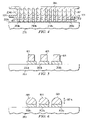
- Solder sheet 101 is positioned between the parts of a die, as shown in the exploded schematic cross section of FIG. 2 .
- the die has first part 201 with a plurality of openings 201 a designed to match the stamping punch 204 and operate as guides to the pins 204 a of the stamping punch 204 .
- the second part 202 of the die is adjacent the surface 203 a of the workpiece 203 (primary forms of the workpiece include for example a wafer, semiconductor chip, package, and substrate).
- the first part 201 of the die is referred to as the “stripper”, and the second part 202 as the “die” (in a narrow sense).
- the preparation includes a solderable contact surface such as copper with a flash of gold or palladium.
- the pattern of pins 204 a is matched by the openings 201 a of the die and the contact pads 203 b of the workpiece 203 .
- the cross sectional area of these pins (viewed along the length of the pin) contains the other two dimensions effective for determining the volume of the interconnection elements.
- the cross sectional shape of these stamping pins may be round, elliptical, square, rectangular, or any other suitable configuration.
- Solder sheet 101 is clamped between first die part 201 and second die part 202 , as shown in FIG. 3 .
- Stamping punch 204 and the die parts 201 and 202 are aligned with one another, with the clamped sheet 101 in between the parts, and the workpiece 203 so that each stamping pin 204 a is located over one of the contact pads 203 b.
- the stamping punch 204 is pressed through the die parts 201 and 202 , and through solder sheet 101 so that each pin 204 a punches a platelet 401 from sheet 101 (see FIG. 4 ).
- One platelet 401 is created for each contact pad area 203 b on workpiece 203 ; consequently, no contact pad 203 b is left without a solder platelet 401 .
- FIG. 5 is a magnified cross sectional view of platelets 401 after they have been brought in surface contact with contact pads 203 b .
- the stamping method creates solder platelets of substantially equal size and volume. The height is determined by the thickness 102 of the solder sheet 101 , and the area is determined by the cross section of pins 204 a , which, in turn, has been selected to be approximately equal to the area of contact pads 203 b.
- Solder flux may be applied to the contact pads 203 b prior to aligning the die and solder sheet with the workpiece. Consequently, after applying heat to the individual solder platelets and the workpiece, the platelet melts and wets pad 203 b .
- surface tension has formed “balls” 601 (more precisely “half-domes”) out of the melted solder. All balls 601 have substantially the same solder volume, and they have substantially the same height 601 a since they completely cover the equal area of contacts 203 b.
- the method of the invention allows the fabrication of interconnection elements over a wide range of solder ball sizes.
- solder ball sizes typically solder ball heights are between 0.1 to 0.3 mm.
- the assembly is by flip-chip surface mount.
- workpiece 203 is a semiconductor package, or a substrate, and the pads 203 b are package contact pads, or substrate contact pads, respectively, typical solder ball heights are 0.5 mm and thus considerably more voluminous.
- the semiconductor packages may include ball grid array packages, chip-scale packages, chip-size packages, or any packages assembled to outside parts by means of surface mount and reflow materials.
- the schematic cross section of FIG. 7 describes the typical result of surface mount assembly of a workpiece 203 onto the contact pads 701 of a substrate 702 .
- the solder balls 601 of FIG. 6 are reflowed a second time; under pressure, they deform into the bulgy shape of the interconnections 703 , characterized by the protruding center regions 703 a and the comparatively narrower solder joints 703 b.
- FIGS. 8A and 8B to 12 describe the process steps for other embodiments of the invention, comprising the fabrication of composite contact members, which are partly reflowable and partly non-reflowable, and the subsequent assembly of these members on the IC contact pads of a semiconductor wafer, or respectively, their assembly on the contact pads of a semiconductor package or a substrate such as a printed circuit board.
- the process flow starts with the layered sheet or ribbon generally designated 800 in FIG. 8A .
- the sheet has uniform thickness 801 .
- Thickness 801 determines the height of the interconnection members-to-be-fabricated.
- the cross section of FIG. 8B describes the layered structure of sheet 800 .
- the composition and fabrication of sheet 800 insures low cost.
- the relatively thick core layer 810 is made of non-reflowable metal, preferably of low modulus material, selected from a group consisting of aluminum, copper, nickel, cobalt, titanium, tantalum, tungsten, tin, lead and alloys thereof (tin and lead are only used in the temperature range below their reflow temperature).
- a preferred low cost choice is aluminum.
- an additional adherent layer 811 of solderable material is on both surfaces of the core layer 810 .
- the additional metal is selected from a group consisting of copper, nickel, cobalt, gold, silver, palladium, and alloys thereof.
- the solderable layer 811 may be thin.
- the outermost surfaces of sheet 800 are adherent layers of reflowable material.
- the reflowable materials are selected from a group consisting of tin, tin alloys including tin/copper, tin/indium, tin/silder, tin/bismuth, tin/lead, or indium.
- the reflowable layer 812 which will be used for the first interconnect, has a higher reflow temperature than the reflowable layer 813 , which will be used for the second interconnect.
- sheet 800 is positioned between a die having a first part 901 with a plurality of openings 901 a designed to match the stamping punch and operate as guides to the pins of the stamping punch.
- the second part of the die is designated 902 ; it faces the surface 903 a of the workpiece 903 .
- workpieces include a semiconductor wafer, a device package, and a substrate such as a printed circuit board.
- the plurality of contact pads 903 b On the surface 903 a of workpiece 903 are the plurality of contact pads 903 b , which are made of solderable metal and have been prepared to accept the connection members-to-be-formed. To improve solderability, the preparation may include the deposition of flux.
- FIG. 9 Also shown in FIG. 9 is the schematic cross section of the stamping punch 904 with the plurality of stamping pins 904 a .
- the pattern of pins 904 a is matched by the openings 901 a of the die and the contact pads 903 b of the workpiece 903 .
- the diameter of these pins determines the diameter of the members-to-be-fabricated.
- the stamping pins have cross sections selected to include a circle, an ellipse, a square and a rectangle; the pins may also have cross section of other suitable configurations.
- FIG. 10 illustrates the process step of clamping the sheet 800 between first die part 901 and second die part 902 . Further shown in FIG. 10 is the process step of aligning the stamping punch 904 , the die parts 901 and 902 with the clamped sheet 800 in between the parts, and the workpiece 903 so that each stamp pin 904 a is located over one of the contact pads 903 b.
- the stamping punch 904 is pressed through the die parts 901 and 902 , and through sheet 800 so that each stamping pin 904 a punches a member 1101 from sheet 800 .
- one member 1101 is created for each contact pad area 903 b on workpiece 903 . No contact pads 903 b are left without a connection member 1101 .
- FIG. 12 illustrates a small number of these connection members 1101 after they have been brought in surface contact with contact pads 903 b .
- the stamping method creates members of equal height 1101 b , each member having uniform diameter over the complete height.
- the diameter 1101 a is the diameter of the punching pin.
- the height 1101 b is determined by the thickness 801 of the sheet 800
- the diameter 1101 a is determined by the diameter of stamping pin 904 a .
- the core portion 1201 of members 1101 is a non-reflowable material determined by the selection of the core layer 810 of sheet 800 ; preferred examples include aluminum or copper.
- the solderable surface on each end of the members may have to be created by an adherent layer 1202 of solderable metal (for example copper or gold), if the non-reflowable metal 1201 is not solderable by nature.
- Layers 1203 and 1204 are made of reflowable material. Preferably, the material selected for layer 1204 has a higher reflow temperature than the material selected for layer 1203 . In FIG. 12 , layers 1204 have already reflowed in order to attach members 1101 to contact pads 903 b of workpiece 903 . Layers 1203 have reflowed and solidified and are still operable for reflow attachment to external parts at a lower reflow temperature.
- Solder flux may be applied to the contact pads 903 b prior to aligning the die and sheet with the workpiece. Consequently, after applying heat to the individual connection members and the workpiece, the layers 1203 and 1204 will melt, layer 1204 wetting the whole area of contact pad 903 b .
- This reflow process step is indicated in FIG. 12 by the bulging perimeter contours of layers 1204 and the radius of the corners of 1203 .
- FIG. 13 describes the typical result of a flip-chip surface mount assembly of a chip or package 903 onto the contact pads 1301 of a substrate 1302 .
- the assembly is heated to the reflow temperature of layer 1203 so that the reflowable material of layer 1203 is melting. Under the slight pressure of assembly, layers 1203 deform into the somewhat bulgy perimeter indicated in FIG. 13 .
- the non-reflowable columns 1201 of the members remain unchanged by the assembly temperature: cylinders or cubes of uniform diameter (dependent on the cylinder or cube cross section) and uniform height, positioned vertically relative to the plane of the substrate pads 1301 .
- the standoff 705 is 180 ⁇ m, while bulge 703 a has a diameter 704 of 270 ⁇ m.
- the contact pad 203 b (made of copper) of the device has a diameter 706 of 140 ⁇ m
- the contact pad 701 (made of copper) of the board has a diameter 707 of 175 ⁇ m.
- the board 702 typically has a higher coefficient of thermal expansion than the device 203 . Consequently, stress is created at the solder joint during temperature cycling, as it is experienced during reliability testing from ⁇ 40 to +150° C. or in device operation. For the geometries involved, a calculation of the moment of inertia shows an estimated 260E6 ⁇ mE4.
- the standoff 1305 is 180 ⁇ m, while the diameter 1304 of the connection column is 140 ⁇ m throughout the length of the column.
- the contact pad 903 b of the device has a diameter 1306 of 140 ⁇ m, the contact pad 1301 of the board has a diameter 1307 of 175 ⁇ m.
- the board 1302 typically has a higher coefficient of thermal expansion than the device 903 . Consequently, stress is created at the solder joint during temperature cycling, as it is experienced during reliability testing from ⁇ 40 to +150° C. or in device operation.
- a calculation of the moment of inertia shows an estimated 18 to 19E6 ⁇ mE4. This value is a 13 ⁇ improvement over the value calculated for the assembly in FIG. 7 . Even with a 30% increase in Young's moduli (relative to solder) and the same displacement, this improvement translates into a reduced stress by at least a factor of 10.
Abstract
An integrated circuit chip 903, which has a plurality of pads 903 b and non-reflowable contact members 1201 to be connected by reflow attachment to external parts. Each of these contact members 1201 has a height-to-diameter ratio and uniform diameter favorable for absorbing strain under thermo-mechanical stress. The members have a solderable surface 1202 on each end and a layer of reflowable material on each end. Each member is solder-attached (1204) at one end to a chip contact pad 903 b, while the other end (1203) of each member is operable for reflow attachment to external parts.
Description
This application claims priority under 35 USC 119 (e) (1) of provisional application Nos. 60/437,593 filed Dec. 31, 2002 and 60/437,366 filed Dec. 31, 2002.
The present invention is related in general to the field of semiconductor devices and processes and more specifically to the structure and method of interconnection members of integrated circuit chips and packages.
During and after assembly of an integrated circuit (IC) chip to an external part such as a substrate or circuit board by solder reflow, and then during device operation, significant temperature differences and temperature cycles appear between the semiconductor chip and the substrate. This is especially true of flip-chip type mounting schemes. The reliability of the solder joint is strongly influenced by the coefficients of thermal expansion of the semiconductor material and the substrate material. For example, there is more than one order of magnitude difference between the coefficients of thermal expansion of silicon and FR-4. This difference causes thermomechanical stresses, most of which are absorbed by the solder joints.
Thermomechanical stress difficulties are aggravated by coplanarity problems of the solder balls and the difficulties involved in obtaining a favorable height-to-diameter ratio and uniformity of the solder interconnection. These difficulties start with the solder ball attach process. As an example, when solder paste is dispensed, the volume of solder paste may vary in volume, making it difficult to control the solder ball height. When prefabricated solder balls are used, the difficulty of avoiding a missed attachment site is well known. A coherent, low-cost method is needed to fabricate solder balls of uniform volume and deliver them to the attachment site without missing a site. The method should be flexible enough to be applied for different semiconductor product families and a wide spectrum of design and process variations.
Furthermore, evidence suggests that solder connections of short length and non-uniform width are unfavorable for stress distribution and strain absorption. The stress remains concentrated in the region of the chip-side solder joint, where it may lead to early material fatigue and crack phenomena. Accordingly, solder connections of generally spherical shape are likely to be more sensitive to stress than elongated connections.
The fabrication methods and reliability problems involving flip-chips re-appear, in somewhat modified form, for ball-grid array type packages, including chip-scale packages (CSP). Most CSP approaches are based on flip-chip assembly with solder bumps or solder balls on the exterior of the package, to interface with system or wiring boards.
Following the solder reflow step, flip-assembled chips and packages often use a polymeric underfill between the chip, or package, and the interposer, substrate, or printed circuit board (PCB). These underfill materials alleviate some of the thermomechanical stress caused by the mismatch of the coefficients of thermal expansion (CTE) of package components. But as a process step, underfilling is time-consuming and expensive, and is preferably avoided.
During the last decade, a number of variations in device structure, materials, or process steps have been implemented in manufacturing in order to alleviate the thermomechanical stress problem. All of them suffer from some drawback in cost, fabrication flow, material selection, and so forth.
A need has therefore arisen for a coherent, low-cost method of assembling flip-chip integrated circuit chips and semiconductor devices that provides a high degree of thermomechanical stress reliability. The method should be flexible enough to be applied for different semiconductor product families and a wide spectrum of design and process variations. Preferably, these innovations should be accomplished using the installed equipment base so that no investment in new manufacturing machines is needed.
One embodiment of the invention comprises a method for forming interconnection elements, such as solder balls, of uniform volume and assembling these elements on the integrated circuit (IC) contact pads of a semiconductor wafer, without missing a contact pad. The thickness of a sheet of solder material determines one dimension of the volume of the interconnection elements.
Further provided is a two-part die for guiding a stamping punch; each part has a structure to match the pattern of the IC pads. The solder sheet is clamped between the die parts. A stamping punch has a plurality of stamping pins; the cross section area of the pins determines the other dimensions of the solder ball volume. The pins are distributed to match the distribution of the circuit pads. The stamping punch, the die with the clamped solder sheet, and the semiconductor wafer are aligned so that each stamp pin is located over one of the circuit pads. The punch is pressed through the die and the sheet so that each pin stamps out a platelet from the sheet, creating one platelet for each pad area. The platelets are brought in surface contact with the pads. Heat is then applied to the individual solder platelets and the wafer to melt the platelets. Finally, the melted solder reflows to form an interconnection element, or solder ball, at each contact pad area.
It is a technical advantage of the method of the invention that all interconnection elements for an IC wafer are created in a batch process, have the same volume, and no contact pads can be missed. The method is low-cost and reliable.
In another embodiment of the invention, the method is applied to batch-process forming of the interconnection elements and assembling the elements on the contact pads of a semiconductor package. It is a technical advantage of the invention that the method can be applied to many families of surface-mount packages such as ball grid array packages, chip-scale packages, and chip-size packages.
Another embodiment of the invention comprises an integrated circuit chip, which has a plurality of pads and contact members composed of layers of materials. The layers of the members are chosen to provide for reflow attach at both ends, and a non-reflowable core which retains its geometry so as to distribute the thermo-mechanical stresses away from the reflowed joints after assembly. Each member is solder-attached at one end to a chip contact pad, while the other end of each member is operable for reflow attachment to external parts.
The height-to-diameter ratio of the contact members is preferably >/=1 and the diameter of the non-reflowable core stays constant after reflow attachment. Preferably, the core of the members is made of a low modulus material; preferred choices include aluminum, copper, nickel, cobalt, titanium, tantalum, tungsten, tin, lead, and alloys thereof. The end surfaces of the core material may have an adherent layer of solderable metal, including copper, nickel, cobalt, gold, palladium, and alloys thereof. The members may have an additional layer of reflowable material at each end, preferably a tin alloy, or a conductive adhesive compound.
The member is to be stamped from a multi-layer sheet or strip. It is an advantage to manufacture the multi-layer sheet in strip or sheet form, as efficient processes like cladding or high-speed plating can be used. It is an advantage for many applications to select the reflowable material layers so that the material at the first end to be reflowed has a higher reflow temperature than the material intended for secondary attachment. The stamping process can be integrated with the placement of the members on to the chip or package contact pads.
Yet another embodiment of the invention comprises a semiconductor package, such as a ball grid array or a chip-scale package, which has a plurality of pads and contact members composed of layers of materials. The layers of the members are chosen to provide for reflow attach at both ends, and a non-reflowable core which retains its geometry so as to distribute the thermo-mechanical stresses away from the reflow joints after assembly. Each of these contact members is solder-attached at one end to a package contact pad, while the other end of each member is operable for reflow attachment to external parts.
The process flow for fabricating non-reflowable contact members and assembling these members on the integrated circuit pads of semiconductor wafers, or package pads of semiconductor devices, starts with providing a metal sheet, which has a core layer of non-reflowable metal and a layer of reflowable material on each surface. The thickness of the sheet is selected so that it will determine the height of the member-to-be-fabricated.
Further provided is a two-part die for guiding a stamping punch, each part having a structure to match the pattern of the IC pads, or package pads. The multi-layer sheet is clamped between the die parts. The stamping punch has a plurality of stamping pins with a diameter, which determines the diameter of the members-to-be-fabricated. The distribution of the pins matches the distribution of the contact pads.
The stamping punch, the die with the clamped sheet, and the semiconductor wafer (or package, respectively) are aligned so that each stamp pin is located over one of the contact pads. Pressing the punch through the die and the sheet stamps out a member of the sheet and creates one member for each pad area. After the members and the pads are brought into contact, heat is applied until the reflowable material between the members and the pads is melting. When the temperature is lowered again below the reflow temperature, each member becomes firmly attached to its respective contact pad.
It is a technical advantage of the method of the invention that the height-to-diameter ratio of the connection members is controlled by the choice of the metal sheet thickness and the stamping punch pin diameter. The distribution of the mechanical stress can thus be controlled.
Another advantage of the invention is the wide range of material variation available for the choice of the connection members, enabled by the selection of the non-reflowable metal sheet, its wettable surfaces, and its reflowable material layers.
The technical advances represented by the invention, as well as the aspects thereof, will become apparent from the following description of the preferred embodiments of the invention, when considered in conjunction with the accompanying drawings and the novel features set forth in the appended claims.
The schematic FIGS. 1 to 6 describe process steps for one embodiment of the invention, comprising the fabrication of interconnection elements of substantially uniform volume and the assembly of these interconnection elements on the integrated circuit (IC) contact pads of a semiconductor wafer, a singulated chip, or their assembly on the contact pads of a semiconductor package or a substrate such as a printed circuit board. One result of the inventive method is that all interconnection elements have substantially the same volume and the same height.
A first embodiment process flow starts with a sheet or ribbon of solder material 101, as depicted in FIG. 1 . The solder material can be selected from a group consisting of tin, tin alloys including tin/copper, tin/indium, tin/silver, tin/bismuth, tin/lead, or indium; in other embodiments, the sheet may comprise conductive adhesive compounds or similar materials. The sheet or ribbon 101 has uniform thickness 102. Thickness 102 determines one dimension of the resulting interconnection elements.
The pattern of pins 204 a is matched by the openings 201 a of the die and the contact pads 203 b of the workpiece 203. The cross sectional area of these pins (viewed along the length of the pin) contains the other two dimensions effective for determining the volume of the interconnection elements. The cross sectional shape of these stamping pins may be round, elliptical, square, rectangular, or any other suitable configuration.
The stamping punch 204 is pressed through the die parts 201 and 202, and through solder sheet 101 so that each pin 204 a punches a platelet 401 from sheet 101 (see FIG. 4 ). One platelet 401 is created for each contact pad area 203 b on workpiece 203; consequently, no contact pad 203 b is left without a solder platelet 401.
Solder flux may be applied to the contact pads 203 b prior to aligning the die and solder sheet with the workpiece. Consequently, after applying heat to the individual solder platelets and the workpiece, the platelet melts and wets pad 203 b. In FIG. 6 , surface tension has formed “balls” 601 (more precisely “half-domes”) out of the melted solder. All balls 601 have substantially the same solder volume, and they have substantially the same height 601 a since they completely cover the equal area of contacts 203 b.
The method of the invention allows the fabrication of interconnection elements over a wide range of solder ball sizes. As an example, when workpiece 203 is a silicon wafer and the pads 203 b are the contact pads of an IC, typical solder ball heights are between 0.1 to 0.3 mm. The assembly is by flip-chip surface mount. As another example, when workpiece 203 is a semiconductor package, or a substrate, and the pads 203 b are package contact pads, or substrate contact pads, respectively, typical solder ball heights are 0.5 mm and thus considerably more voluminous. The semiconductor packages may include ball grid array packages, chip-scale packages, chip-size packages, or any packages assembled to outside parts by means of surface mount and reflow materials.
The schematic cross section of FIG. 7 describes the typical result of surface mount assembly of a workpiece 203 onto the contact pads 701 of a substrate 702. The solder balls 601 of FIG. 6 are reflowed a second time; under pressure, they deform into the bulgy shape of the interconnections 703, characterized by the protruding center regions 703 a and the comparatively narrower solder joints 703 b.
The schematic FIGS. 8A and 8B to 12 describe the process steps for other embodiments of the invention, comprising the fabrication of composite contact members, which are partly reflowable and partly non-reflowable, and the subsequent assembly of these members on the IC contact pads of a semiconductor wafer, or respectively, their assembly on the contact pads of a semiconductor package or a substrate such as a printed circuit board.
The process flow starts with the layered sheet or ribbon generally designated 800 in FIG. 8A . The sheet has uniform thickness 801. Thickness 801 determines the height of the interconnection members-to-be-fabricated.
The cross section of FIG. 8B describes the layered structure of sheet 800. The composition and fabrication of sheet 800 insures low cost. The relatively thick core layer 810 is made of non-reflowable metal, preferably of low modulus material, selected from a group consisting of aluminum, copper, nickel, cobalt, titanium, tantalum, tungsten, tin, lead and alloys thereof (tin and lead are only used in the temperature range below their reflow temperature). A preferred low cost choice is aluminum. When the metal of layer 810 is not solderable, an additional adherent layer 811 of solderable material is on both surfaces of the core layer 810. Preferably, the additional metal is selected from a group consisting of copper, nickel, cobalt, gold, silver, palladium, and alloys thereof. Compared to the thick core layer 810, the solderable layer 811 may be thin.
The outermost surfaces of sheet 800 are adherent layers of reflowable material. The reflowable materials are selected from a group consisting of tin, tin alloys including tin/copper, tin/indium, tin/silder, tin/bismuth, tin/lead, or indium. In the preferred embodiment, the reflowable layer 812, which will be used for the first interconnect, has a higher reflow temperature than the reflowable layer 813, which will be used for the second interconnect.
As shown in FIG. 9 , sheet 800 is positioned between a die having a first part 901 with a plurality of openings 901 a designed to match the stamping punch and operate as guides to the pins of the stamping punch. The second part of the die is designated 902; it faces the surface 903 a of the workpiece 903. Examples of workpieces include a semiconductor wafer, a device package, and a substrate such as a printed circuit board. On the surface 903 a of workpiece 903 are the plurality of contact pads 903 b, which are made of solderable metal and have been prepared to accept the connection members-to-be-formed. To improve solderability, the preparation may include the deposition of flux.
Also shown in FIG. 9 is the schematic cross section of the stamping punch 904 with the plurality of stamping pins 904 a. The pattern of pins 904 a is matched by the openings 901 a of the die and the contact pads 903 b of the workpiece 903. The diameter of these pins determines the diameter of the members-to-be-fabricated. The stamping pins have cross sections selected to include a circle, an ellipse, a square and a rectangle; the pins may also have cross section of other suitable configurations.
In the next process step, depicted in FIG. 11 , the stamping punch 904 is pressed through the die parts 901 and 902, and through sheet 800 so that each stamping pin 904 a punches a member 1101 from sheet 800. In this process step, one member 1101 is created for each contact pad area 903 b on workpiece 903. No contact pads 903 b are left without a connection member 1101.
In a magnified cross sectional view, FIG. 12 illustrates a small number of these connection members 1101 after they have been brought in surface contact with contact pads 903 b. As can be seen, the stamping method creates members of equal height 1101 b, each member having uniform diameter over the complete height. The diameter 1101 a is the diameter of the punching pin. For absorbing strain under thermomechanical stress, the preferred height-to-diameter ratio is >/=1. The height 1101 b is determined by the thickness 801 of the sheet 800, and the diameter 1101 a is determined by the diameter of stamping pin 904 a. The core portion 1201 of members 1101 is a non-reflowable material determined by the selection of the core layer 810 of sheet 800; preferred examples include aluminum or copper. The solderable surface on each end of the members may have to be created by an adherent layer 1202 of solderable metal (for example copper or gold), if the non-reflowable metal 1201 is not solderable by nature. Layers 1203 and 1204 are made of reflowable material. Preferably, the material selected for layer 1204 has a higher reflow temperature than the material selected for layer 1203. In FIG. 12 , layers 1204 have already reflowed in order to attach members 1101 to contact pads 903 b of workpiece 903. Layers 1203 have reflowed and solidified and are still operable for reflow attachment to external parts at a lower reflow temperature.
Solder flux may be applied to the contact pads 903 b prior to aligning the die and sheet with the workpiece. Consequently, after applying heat to the individual connection members and the workpiece, the layers 1203 and 1204 will melt, layer 1204 wetting the whole area of contact pad 903 b. This reflow process step is indicated in FIG. 12 by the bulging perimeter contours of layers 1204 and the radius of the corners of 1203.
The schematic cross section of FIG. 13 describes the typical result of a flip-chip surface mount assembly of a chip or package 903 onto the contact pads 1301 of a substrate 1302. The assembly is heated to the reflow temperature of layer 1203 so that the reflowable material of layer 1203 is melting. Under the slight pressure of assembly, layers 1203 deform into the somewhat bulgy perimeter indicated in FIG. 13 . In contrast to the solder layers 1203, the non-reflowable columns 1201 of the members remain unchanged by the assembly temperature: cylinders or cubes of uniform diameter (dependent on the cylinder or cube cross section) and uniform height, positioned vertically relative to the plane of the substrate pads 1301.
Referring now to FIG. 7 , in a mass-produced device by way of example, the standoff 705 is 180 μm, while bulge 703 a has a diameter 704 of 270 μm. In this device, the contact pad 203 b (made of copper) of the device has a diameter 706 of 140 μm, the contact pad 701 (made of copper) of the board has a diameter 707 of 175 μm. The board 702 typically has a higher coefficient of thermal expansion than the device 203. Consequently, stress is created at the solder joint during temperature cycling, as it is experienced during reliability testing from −40 to +150° C. or in device operation. For the geometries involved, a calculation of the moment of inertia shows an estimated 260E6 μmE4.
This value is to be compared to the same device having the column-shaped members of FIG. 13 . The standoff 1305 is 180 μm, while the diameter 1304 of the connection column is 140 μm throughout the length of the column. The contact pad 903 b of the device has a diameter 1306 of 140 μm, the contact pad 1301 of the board has a diameter 1307 of 175 μm. The board 1302 typically has a higher coefficient of thermal expansion than the device 903. Consequently, stress is created at the solder joint during temperature cycling, as it is experienced during reliability testing from −40 to +150° C. or in device operation. For the geometries involved, a calculation of the moment of inertia shows an estimated 18 to 19E6 μmE4. This value is a 13× improvement over the value calculated for the assembly in FIG. 7 . Even with a 30% increase in Young's moduli (relative to solder) and the same displacement, this improvement translates into a reduced stress by at least a factor of 10.
While this invention has been described in reference to illustrative embodiments, this description is not intended to be construed in a limiting sense. Various modifications and combinations of the illustrative embodiments, as well as other embodiments of the invention, will be apparent to persons skilled in the art upon reference to the description. As an example, the concept of punching, on the location of usage, a plurality of non-reflowable interconnections of equal height from a sheet of starting material and then affixing these interconnections in the assembly of one part with another part, can be applied to a wide range of products. These products can especially be found in, but are not limited to, electronics boards composed of a variety of different components. It is therefore intended that the appended claims encompass any such modifications or embodiments.
Claims (5)
1. A method for forming connection members and assembling said members on the contact pads on a semiconductor device comprising the steps of:
providing a metal sheet with a top surface and a bottom, having a core layer of a non-reflowable metal and a layer of reflowable material adherent to each surface, the thickness of said sheet determining the height of said connection members;
providing a two-part die for guiding a stamping punch, each part having a structure to match the pattern of said contact pads;
positioning and clamping said sheet between said die parts;
providing a stamping punch having a plurality of stamping pins, the diameter of said pins determining the diameter of said connection members, said pins distributed to match said contact pad distribution;
aligning said punch, said die having said sheet clamped between said parts and said semiconductor device so that each stamp pin is located over one of said contact pads;
pressing said punch through said die and said sheet so that each stamping pin punches a connection member from said sheet, creating one connection member for each contact pad;
bringing said members in surface contact with said pads;
applying heat to said individual members and said device to melt said reflowable material between said members and said pads; and
cooling the temperature below the reflow temperature whereby each member becomes firmly attached to its respective pad.
2. The method according to claim 1 wherein solder flux is applied to said contact pads prior to aligning said die and sheet with said wafer.
3. The method according to claim 1 wherein said members are positioned vertically relative to the plane of said pads.
4. The method according to claim 1 wherein all said connection members are of substantially the same size.
5. The method according to claim 1 wherein said stamping pins are shaped as cylinders having a cross section selected from a group consisting of round, elliptical, square, and rectangular.
Priority Applications (2)
| Application Number | Priority Date | Filing Date | Title |
|---|---|---|---|
| US10/732,666 US7125789B2 (en) | 2002-12-31 | 2003-12-08 | Composite metal column for mounting semiconductor device |
| US11/470,541 US7550852B2 (en) | 2002-12-31 | 2006-09-06 | Composite metal column for mounting semiconductor device |
Applications Claiming Priority (3)
| Application Number | Priority Date | Filing Date | Title |
|---|---|---|---|
| US43736602P | 2002-12-31 | 2002-12-31 | |
| US43759302P | 2002-12-31 | 2002-12-31 | |
| US10/732,666 US7125789B2 (en) | 2002-12-31 | 2003-12-08 | Composite metal column for mounting semiconductor device |
Related Child Applications (1)
| Application Number | Title | Priority Date | Filing Date |
|---|---|---|---|
| US11/470,541 Division US7550852B2 (en) | 2002-12-31 | 2006-09-06 | Composite metal column for mounting semiconductor device |
Publications (2)
| Publication Number | Publication Date |
|---|---|
| US20040135251A1 US20040135251A1 (en) | 2004-07-15 |
| US7125789B2 true US7125789B2 (en) | 2006-10-24 |
Family
ID=32659480
Family Applications (1)
| Application Number | Title | Priority Date | Filing Date |
|---|---|---|---|
| US10/732,666 Active 2024-07-21 US7125789B2 (en) | 2002-12-31 | 2003-12-08 | Composite metal column for mounting semiconductor device |
Country Status (5)
| Country | Link |
|---|---|
| US (1) | US7125789B2 (en) |
| EP (1) | EP1443548A3 (en) |
| JP (1) | JP2004214676A (en) |
| KR (1) | KR20040062411A (en) |
| TW (1) | TW200423344A (en) |
Cited By (14)
| Publication number | Priority date | Publication date | Assignee | Title |
|---|---|---|---|---|
| US20090146303A1 (en) * | 2007-09-28 | 2009-06-11 | Tessera, Inc. | Flip Chip Interconnection with double post |
| US20090188706A1 (en) * | 2007-12-25 | 2009-07-30 | Tessera Interconnect Materials, Inc. | Interconnection element for electric circuits |
| US20110068465A1 (en) * | 2009-09-18 | 2011-03-24 | Taiwan Semiconductor Manufacturing Company, Ltd. | Strong interconnection post geometry |
| US8330272B2 (en) | 2010-07-08 | 2012-12-11 | Tessera, Inc. | Microelectronic packages with dual or multiple-etched flip-chip connectors |
| CN102832144A (en) * | 2011-06-15 | 2012-12-19 | 台湾积体电路制造股份有限公司 | Metal bump formation |
| US8462516B2 (en) | 2007-11-06 | 2013-06-11 | Agency For Science Technology And Research | Interconnect structure and a method of fabricating the same |
| US8531039B2 (en) | 2003-12-30 | 2013-09-10 | Tessera, Inc. | Micro pin grid array with pin motion isolation |
| US8580607B2 (en) | 2010-07-27 | 2013-11-12 | Tessera, Inc. | Microelectronic packages with nanoparticle joining |
| US8604348B2 (en) | 2003-10-06 | 2013-12-10 | Tessera, Inc. | Method of making a connection component with posts and pads |
| US8641913B2 (en) | 2003-10-06 | 2014-02-04 | Tessera, Inc. | Fine pitch microcontacts and method for forming thereof |
| US8853558B2 (en) | 2010-12-10 | 2014-10-07 | Tessera, Inc. | Interconnect structure |
| US9633971B2 (en) | 2015-07-10 | 2017-04-25 | Invensas Corporation | Structures and methods for low temperature bonding using nanoparticles |
| US10103121B2 (en) | 2015-08-21 | 2018-10-16 | Invensas Corporation | Tall and fine pitch interconnects |
| US10535626B2 (en) | 2015-07-10 | 2020-01-14 | Invensas Corporation | Structures and methods for low temperature bonding using nanoparticles |
Families Citing this family (10)
| Publication number | Priority date | Publication date | Assignee | Title |
|---|---|---|---|---|
| US20040007779A1 (en) * | 2002-07-15 | 2004-01-15 | Diane Arbuthnot | Wafer-level method for fine-pitch, high aspect ratio chip interconnect |
| US6929170B2 (en) * | 2003-09-30 | 2005-08-16 | Ted Ju | Solder deposition method |
| JP4576270B2 (en) * | 2005-03-29 | 2010-11-04 | 昭和電工株式会社 | Method for manufacturing solder circuit board |
| WO2007007865A1 (en) | 2005-07-11 | 2007-01-18 | Showa Denko K.K. | Method for attachment of solder powder to electronic circuit board and solder-attached electronic circuit board |
| US20090041990A1 (en) * | 2005-09-09 | 2009-02-12 | Showa Denko K.K. | Method for attachment of solder powder to electronic circuit board and soldered electronic circuit board |
| US20090261148A1 (en) * | 2006-08-03 | 2009-10-22 | Showa Denko K.K. | Production method of solder circuit board |
| JP5608824B2 (en) * | 2011-12-27 | 2014-10-15 | パナソニック株式会社 | Bonding structure |
| CN105448872A (en) * | 2014-08-29 | 2016-03-30 | 展讯通信(上海)有限公司 | Improved chip connection structure and manufacturing process thereof |
| CN111394612B (en) * | 2020-04-29 | 2023-10-20 | 西安同为工业技术有限公司 | Anti-scaling device based on cross or snowflake hole type alloy material chip |
| CN114986012A (en) * | 2022-06-06 | 2022-09-02 | 中国科学院宁波材料技术与工程研究所 | Composite columnar soft soldering material and preparation method and application thereof |
Citations (8)
| Publication number | Priority date | Publication date | Assignee | Title |
|---|---|---|---|---|
| US5130779A (en) | 1990-06-19 | 1992-07-14 | International Business Machines Corporation | Solder mass having conductive encapsulating arrangement |
| EP0704895A2 (en) | 1994-09-30 | 1996-04-03 | Nec Corporation | Process for manufacturing semiconductor device and semiconductor wafer |
| WO1997019466A1 (en) | 1995-11-22 | 1997-05-29 | Fry's Metals, Inc. | Method and apparatus for forming solder bumps on a substrate |
| US6024275A (en) | 1997-06-18 | 2000-02-15 | National Semiconductor Corporation | Method of making flip chip and BGA interconnections |
| US6077380A (en) | 1995-06-30 | 2000-06-20 | Microfab Technologies, Inc. | Method of forming an adhesive connection |
| US6249963B1 (en) | 1996-11-27 | 2001-06-26 | Texas Instruments Incorporated | System and method for coupling conductive pellets to a component of an integrated circuit |
| US20030038162A1 (en) * | 2001-08-21 | 2003-02-27 | Chew Jimmy Hwee Seng | Method for forming a flip chip on leadframe semiconductor package |
| US20040087057A1 (en) * | 2002-10-30 | 2004-05-06 | Advanpack Solutions Pte. Ltd. | Method for fabricating a flip chip package with pillar bump and no flow underfill |
-
2003
- 2003-11-04 TW TW092130857A patent/TW200423344A/en unknown
- 2003-12-08 US US10/732,666 patent/US7125789B2/en active Active
- 2003-12-24 EP EP03104978A patent/EP1443548A3/en not_active Withdrawn
- 2003-12-26 JP JP2003433883A patent/JP2004214676A/en active Pending
- 2003-12-30 KR KR1020030100234A patent/KR20040062411A/en not_active Application Discontinuation
Patent Citations (8)
| Publication number | Priority date | Publication date | Assignee | Title |
|---|---|---|---|---|
| US5130779A (en) | 1990-06-19 | 1992-07-14 | International Business Machines Corporation | Solder mass having conductive encapsulating arrangement |
| EP0704895A2 (en) | 1994-09-30 | 1996-04-03 | Nec Corporation | Process for manufacturing semiconductor device and semiconductor wafer |
| US6077380A (en) | 1995-06-30 | 2000-06-20 | Microfab Technologies, Inc. | Method of forming an adhesive connection |
| WO1997019466A1 (en) | 1995-11-22 | 1997-05-29 | Fry's Metals, Inc. | Method and apparatus for forming solder bumps on a substrate |
| US6249963B1 (en) | 1996-11-27 | 2001-06-26 | Texas Instruments Incorporated | System and method for coupling conductive pellets to a component of an integrated circuit |
| US6024275A (en) | 1997-06-18 | 2000-02-15 | National Semiconductor Corporation | Method of making flip chip and BGA interconnections |
| US20030038162A1 (en) * | 2001-08-21 | 2003-02-27 | Chew Jimmy Hwee Seng | Method for forming a flip chip on leadframe semiconductor package |
| US20040087057A1 (en) * | 2002-10-30 | 2004-05-06 | Advanpack Solutions Pte. Ltd. | Method for fabricating a flip chip package with pillar bump and no flow underfill |
Cited By (31)
| Publication number | Priority date | Publication date | Assignee | Title |
|---|---|---|---|---|
| US8641913B2 (en) | 2003-10-06 | 2014-02-04 | Tessera, Inc. | Fine pitch microcontacts and method for forming thereof |
| US8604348B2 (en) | 2003-10-06 | 2013-12-10 | Tessera, Inc. | Method of making a connection component with posts and pads |
| US8531039B2 (en) | 2003-12-30 | 2013-09-10 | Tessera, Inc. | Micro pin grid array with pin motion isolation |
| US20090146303A1 (en) * | 2007-09-28 | 2009-06-11 | Tessera, Inc. | Flip Chip Interconnection with double post |
| US8558379B2 (en) | 2007-09-28 | 2013-10-15 | Tessera, Inc. | Flip chip interconnection with double post |
| US20110074027A1 (en) * | 2007-09-28 | 2011-03-31 | Tessera, Inc. | Flip chip interconnection with double post |
| US8884448B2 (en) | 2007-09-28 | 2014-11-11 | Tessera, Inc. | Flip chip interconnection with double post |
| US8462516B2 (en) | 2007-11-06 | 2013-06-11 | Agency For Science Technology And Research | Interconnect structure and a method of fabricating the same |
| US8299368B2 (en) | 2007-12-25 | 2012-10-30 | Invensas Corporation | Interconnection element for electric circuits |
| US20090188706A1 (en) * | 2007-12-25 | 2009-07-30 | Tessera Interconnect Materials, Inc. | Interconnection element for electric circuits |
| US8178970B2 (en) * | 2009-09-18 | 2012-05-15 | Taiwan Semiconductor Manufacturing Company, Ltd. | Strong interconnection post geometry |
| US20110068465A1 (en) * | 2009-09-18 | 2011-03-24 | Taiwan Semiconductor Manufacturing Company, Ltd. | Strong interconnection post geometry |
| US8330272B2 (en) | 2010-07-08 | 2012-12-11 | Tessera, Inc. | Microelectronic packages with dual or multiple-etched flip-chip connectors |
| US8723318B2 (en) | 2010-07-08 | 2014-05-13 | Tessera, Inc. | Microelectronic packages with dual or multiple-etched flip-chip connectors |
| US9397063B2 (en) | 2010-07-27 | 2016-07-19 | Tessera, Inc. | Microelectronic packages with nanoparticle joining |
| US8580607B2 (en) | 2010-07-27 | 2013-11-12 | Tessera, Inc. | Microelectronic packages with nanoparticle joining |
| US9030001B2 (en) | 2010-07-27 | 2015-05-12 | Tessera, Inc. | Microelectronic packages with nanoparticle joining |
| US8853558B2 (en) | 2010-12-10 | 2014-10-07 | Tessera, Inc. | Interconnect structure |
| US9496236B2 (en) | 2010-12-10 | 2016-11-15 | Tessera, Inc. | Interconnect structure |
| US8501615B2 (en) * | 2011-06-15 | 2013-08-06 | Taiwan Semiconductor Manufacturing Company, Ltd. | Metal bump formation |
| US20120322255A1 (en) * | 2011-06-15 | 2012-12-20 | Taiwan Semiconductor Manufacturing Company, Ltd. | Metal Bump Formation |
| CN102832144B (en) * | 2011-06-15 | 2015-10-07 | 台湾积体电路制造股份有限公司 | The formation of metal coupling |
| CN102832144A (en) * | 2011-06-15 | 2012-12-19 | 台湾积体电路制造股份有限公司 | Metal bump formation |
| US9633971B2 (en) | 2015-07-10 | 2017-04-25 | Invensas Corporation | Structures and methods for low temperature bonding using nanoparticles |
| US9818713B2 (en) | 2015-07-10 | 2017-11-14 | Invensas Corporation | Structures and methods for low temperature bonding using nanoparticles |
| US10535626B2 (en) | 2015-07-10 | 2020-01-14 | Invensas Corporation | Structures and methods for low temperature bonding using nanoparticles |
| US10886250B2 (en) | 2015-07-10 | 2021-01-05 | Invensas Corporation | Structures and methods for low temperature bonding using nanoparticles |
| US10892246B2 (en) | 2015-07-10 | 2021-01-12 | Invensas Corporation | Structures and methods for low temperature bonding using nanoparticles |
| US11710718B2 (en) | 2015-07-10 | 2023-07-25 | Adeia Semiconductor Technologies Llc | Structures and methods for low temperature bonding using nanoparticles |
| US10103121B2 (en) | 2015-08-21 | 2018-10-16 | Invensas Corporation | Tall and fine pitch interconnects |
| US10818629B2 (en) | 2015-08-21 | 2020-10-27 | Invensas Corporation | Tall and fine pitch interconnects |
Also Published As
| Publication number | Publication date |
|---|---|
| EP1443548A3 (en) | 2004-08-18 |
| US20040135251A1 (en) | 2004-07-15 |
| JP2004214676A (en) | 2004-07-29 |
| TW200423344A (en) | 2004-11-01 |
| EP1443548A2 (en) | 2004-08-04 |
| KR20040062411A (en) | 2004-07-07 |
Similar Documents
| Publication | Publication Date | Title |
|---|---|---|
| US7125789B2 (en) | Composite metal column for mounting semiconductor device | |
| EP1364401B1 (en) | Microelectronic package having bumpless laminated interconnection layer | |
| JP3262497B2 (en) | Chip mounted circuit card structure | |
| EP0624053B1 (en) | Mounting device and method of connecting miniaturized electronic components by bump connections | |
| US7947602B2 (en) | Conductive pattern formation method | |
| US20090289360A1 (en) | Workpiece contact pads with elevated ring for restricting horizontal movement of terminals of ic during pressing | |
| EP2675254A1 (en) | Surface mount interconnection system for modular circuit board and method | |
| US5650667A (en) | Process of forming conductive bumps on the electrodes of semiconductor chips using lapping and the bumps thereby created | |
| US6348399B1 (en) | Method of making chip scale package | |
| EP2633551B1 (en) | Lead-free structures in a semiconductor device | |
| TW201237976A (en) | Bump-on-lead flip chip interconnection | |
| JP2010541244A (en) | Flip chip interconnect with double posts | |
| EP0473929A1 (en) | Method of forming a thin film electronic device | |
| US20060022320A1 (en) | Semiconductor device and manufacturing method thereof | |
| US7304376B2 (en) | Microelectronic assemblies with springs | |
| US20040235221A1 (en) | Electronic device and method for manufacturing the same | |
| KR20130127919A (en) | Electronic component mounting structure and method of manufacturing electronic component mounting structure | |
| US7550852B2 (en) | Composite metal column for mounting semiconductor device | |
| EP2040296A2 (en) | Method for forming BGA package with increased standoff height | |
| US20020089836A1 (en) | Injection molded underfill package and method of assembly | |
| EP0804056B1 (en) | Improvements in or relating to a connecting board | |
| US20070085220A1 (en) | Re-enforced ball-grid array packages for semiconductor products | |
| JP3838530B2 (en) | Manufacturing method of semiconductor device | |
| JP2000151086A (en) | Printed circuit unit and its manufacture | |
| JPH05102251A (en) | Tab tape, manufacture thereof and ic chip mounting method using said tab tape |
Legal Events
| Date | Code | Title | Description |
|---|---|---|---|
| AS | Assignment |
Owner name: TEXAS INSTRUMENTS INCORPORATED, TEXAS Free format text: ASSIGNMENT OF ASSIGNORS INTEREST;ASSIGNORS:TELLKAMP, JOHN P.;MATSUNAMI, AKIRA;REEL/FRAME:015150/0628;SIGNING DATES FROM 20040105 TO 20040115 |
|
| STCF | Information on status: patent grant |
Free format text: PATENTED CASE |
|
| FPAY | Fee payment |
Year of fee payment: 4 |
|
| FPAY | Fee payment |
Year of fee payment: 8 |
|
| MAFP | Maintenance fee payment |
Free format text: PAYMENT OF MAINTENANCE FEE, 12TH YEAR, LARGE ENTITY (ORIGINAL EVENT CODE: M1553) Year of fee payment: 12 |