US7134827B2 - Reduced footprint tool for automated processing of microelectronic substrates - Google Patents
Reduced footprint tool for automated processing of microelectronic substrates Download PDFInfo
- Publication number
- US7134827B2 US7134827B2 US10/952,506 US95250604A US7134827B2 US 7134827 B2 US7134827 B2 US 7134827B2 US 95250604 A US95250604 A US 95250604A US 7134827 B2 US7134827 B2 US 7134827B2
- Authority
- US
- United States
- Prior art keywords
- substrates
- storage device
- substrate
- wafer transfer
- transfer system
- Prior art date
- Legal status (The legal status is an assumption and is not a legal conclusion. Google has not performed a legal analysis and makes no representation as to the accuracy of the status listed.)
- Expired - Fee Related
Links
Images


Classifications
-
- H—ELECTRICITY
- H01—ELECTRIC ELEMENTS
- H01L—SEMICONDUCTOR DEVICES NOT COVERED BY CLASS H10
- H01L21/00—Processes or apparatus adapted for the manufacture or treatment of semiconductor or solid state devices or of parts thereof
-
- H—ELECTRICITY
- H01—ELECTRIC ELEMENTS
- H01L—SEMICONDUCTOR DEVICES NOT COVERED BY CLASS H10
- H01L21/00—Processes or apparatus adapted for the manufacture or treatment of semiconductor or solid state devices or of parts thereof
- H01L21/67—Apparatus specially adapted for handling semiconductor or electric solid state devices during manufacture or treatment thereof; Apparatus specially adapted for handling wafers during manufacture or treatment of semiconductor or electric solid state devices or components ; Apparatus not specifically provided for elsewhere
- H01L21/67005—Apparatus not specifically provided for elsewhere
- H01L21/67011—Apparatus for manufacture or treatment
- H01L21/67155—Apparatus for manufacturing or treating in a plurality of work-stations
- H01L21/67161—Apparatus for manufacturing or treating in a plurality of work-stations characterized by the layout of the process chambers
- H01L21/67167—Apparatus for manufacturing or treating in a plurality of work-stations characterized by the layout of the process chambers surrounding a central transfer chamber
-
- H—ELECTRICITY
- H01—ELECTRIC ELEMENTS
- H01L—SEMICONDUCTOR DEVICES NOT COVERED BY CLASS H10
- H01L21/00—Processes or apparatus adapted for the manufacture or treatment of semiconductor or solid state devices or of parts thereof
- H01L21/67—Apparatus specially adapted for handling semiconductor or electric solid state devices during manufacture or treatment thereof; Apparatus specially adapted for handling wafers during manufacture or treatment of semiconductor or electric solid state devices or components ; Apparatus not specifically provided for elsewhere
- H01L21/67005—Apparatus not specifically provided for elsewhere
- H01L21/67011—Apparatus for manufacture or treatment
- H01L21/67155—Apparatus for manufacturing or treating in a plurality of work-stations
- H01L21/67161—Apparatus for manufacturing or treating in a plurality of work-stations characterized by the layout of the process chambers
- H01L21/67173—Apparatus for manufacturing or treating in a plurality of work-stations characterized by the layout of the process chambers in-line arrangement
-
- H—ELECTRICITY
- H01—ELECTRIC ELEMENTS
- H01L—SEMICONDUCTOR DEVICES NOT COVERED BY CLASS H10
- H01L21/00—Processes or apparatus adapted for the manufacture or treatment of semiconductor or solid state devices or of parts thereof
- H01L21/67—Apparatus specially adapted for handling semiconductor or electric solid state devices during manufacture or treatment thereof; Apparatus specially adapted for handling wafers during manufacture or treatment of semiconductor or electric solid state devices or components ; Apparatus not specifically provided for elsewhere
- H01L21/67005—Apparatus not specifically provided for elsewhere
- H01L21/67011—Apparatus for manufacture or treatment
- H01L21/67155—Apparatus for manufacturing or treating in a plurality of work-stations
- H01L21/67161—Apparatus for manufacturing or treating in a plurality of work-stations characterized by the layout of the process chambers
- H01L21/67178—Apparatus for manufacturing or treating in a plurality of work-stations characterized by the layout of the process chambers vertical arrangement
-
- H—ELECTRICITY
- H01—ELECTRIC ELEMENTS
- H01L—SEMICONDUCTOR DEVICES NOT COVERED BY CLASS H10
- H01L21/00—Processes or apparatus adapted for the manufacture or treatment of semiconductor or solid state devices or of parts thereof
- H01L21/67—Apparatus specially adapted for handling semiconductor or electric solid state devices during manufacture or treatment thereof; Apparatus specially adapted for handling wafers during manufacture or treatment of semiconductor or electric solid state devices or components ; Apparatus not specifically provided for elsewhere
- H01L21/67005—Apparatus not specifically provided for elsewhere
- H01L21/67011—Apparatus for manufacture or treatment
- H01L21/67155—Apparatus for manufacturing or treating in a plurality of work-stations
- H01L21/67196—Apparatus for manufacturing or treating in a plurality of work-stations characterized by the construction of the transfer chamber
-
- H—ELECTRICITY
- H01—ELECTRIC ELEMENTS
- H01L—SEMICONDUCTOR DEVICES NOT COVERED BY CLASS H10
- H01L21/00—Processes or apparatus adapted for the manufacture or treatment of semiconductor or solid state devices or of parts thereof
- H01L21/67—Apparatus specially adapted for handling semiconductor or electric solid state devices during manufacture or treatment thereof; Apparatus specially adapted for handling wafers during manufacture or treatment of semiconductor or electric solid state devices or components ; Apparatus not specifically provided for elsewhere
- H01L21/677—Apparatus specially adapted for handling semiconductor or electric solid state devices during manufacture or treatment thereof; Apparatus specially adapted for handling wafers during manufacture or treatment of semiconductor or electric solid state devices or components ; Apparatus not specifically provided for elsewhere for conveying, e.g. between different workstations
- H01L21/67763—Apparatus specially adapted for handling semiconductor or electric solid state devices during manufacture or treatment thereof; Apparatus specially adapted for handling wafers during manufacture or treatment of semiconductor or electric solid state devices or components ; Apparatus not specifically provided for elsewhere for conveying, e.g. between different workstations the wafers being stored in a carrier, involving loading and unloading
- H01L21/67769—Storage means
-
- H—ELECTRICITY
- H01—ELECTRIC ELEMENTS
- H01L—SEMICONDUCTOR DEVICES NOT COVERED BY CLASS H10
- H01L21/00—Processes or apparatus adapted for the manufacture or treatment of semiconductor or solid state devices or of parts thereof
- H01L21/67—Apparatus specially adapted for handling semiconductor or electric solid state devices during manufacture or treatment thereof; Apparatus specially adapted for handling wafers during manufacture or treatment of semiconductor or electric solid state devices or components ; Apparatus not specifically provided for elsewhere
- H01L21/677—Apparatus specially adapted for handling semiconductor or electric solid state devices during manufacture or treatment thereof; Apparatus specially adapted for handling wafers during manufacture or treatment of semiconductor or electric solid state devices or components ; Apparatus not specifically provided for elsewhere for conveying, e.g. between different workstations
- H01L21/67763—Apparatus specially adapted for handling semiconductor or electric solid state devices during manufacture or treatment thereof; Apparatus specially adapted for handling wafers during manufacture or treatment of semiconductor or electric solid state devices or components ; Apparatus not specifically provided for elsewhere for conveying, e.g. between different workstations the wafers being stored in a carrier, involving loading and unloading
- H01L21/67778—Apparatus specially adapted for handling semiconductor or electric solid state devices during manufacture or treatment thereof; Apparatus specially adapted for handling wafers during manufacture or treatment of semiconductor or electric solid state devices or components ; Apparatus not specifically provided for elsewhere for conveying, e.g. between different workstations the wafers being stored in a carrier, involving loading and unloading involving loading and unloading of wafers
- H01L21/67781—Batch transfer of wafers
-
- Y—GENERAL TAGGING OF NEW TECHNOLOGICAL DEVELOPMENTS; GENERAL TAGGING OF CROSS-SECTIONAL TECHNOLOGIES SPANNING OVER SEVERAL SECTIONS OF THE IPC; TECHNICAL SUBJECTS COVERED BY FORMER USPC CROSS-REFERENCE ART COLLECTIONS [XRACs] AND DIGESTS
- Y10—TECHNICAL SUBJECTS COVERED BY FORMER USPC
- Y10S—TECHNICAL SUBJECTS COVERED BY FORMER USPC CROSS-REFERENCE ART COLLECTIONS [XRACs] AND DIGESTS
- Y10S414/00—Material or article handling
- Y10S414/135—Associated with semiconductor wafer handling
- Y10S414/137—Associated with semiconductor wafer handling including means for charging or discharging wafer cassette
- Y10S414/138—Wafers positioned vertically within cassette
-
- Y—GENERAL TAGGING OF NEW TECHNOLOGICAL DEVELOPMENTS; GENERAL TAGGING OF CROSS-SECTIONAL TECHNOLOGIES SPANNING OVER SEVERAL SECTIONS OF THE IPC; TECHNICAL SUBJECTS COVERED BY FORMER USPC CROSS-REFERENCE ART COLLECTIONS [XRACs] AND DIGESTS
- Y10—TECHNICAL SUBJECTS COVERED BY FORMER USPC
- Y10S—TECHNICAL SUBJECTS COVERED BY FORMER USPC CROSS-REFERENCE ART COLLECTIONS [XRACs] AND DIGESTS
- Y10S414/00—Material or article handling
- Y10S414/135—Associated with semiconductor wafer handling
- Y10S414/139—Associated with semiconductor wafer handling including wafer charging or discharging means for vacuum chamber
-
- Y—GENERAL TAGGING OF NEW TECHNOLOGICAL DEVELOPMENTS; GENERAL TAGGING OF CROSS-SECTIONAL TECHNOLOGIES SPANNING OVER SEVERAL SECTIONS OF THE IPC; TECHNICAL SUBJECTS COVERED BY FORMER USPC CROSS-REFERENCE ART COLLECTIONS [XRACs] AND DIGESTS
- Y10—TECHNICAL SUBJECTS COVERED BY FORMER USPC
- Y10S—TECHNICAL SUBJECTS COVERED BY FORMER USPC CROSS-REFERENCE ART COLLECTIONS [XRACs] AND DIGESTS
- Y10S414/00—Material or article handling
- Y10S414/135—Associated with semiconductor wafer handling
- Y10S414/141—Associated with semiconductor wafer handling includes means for gripping wafer
Abstract
The present invention provides tools and methods of processing microelectronic substrates in which the tools maintain high throughput yet have dramatically lower footprint than conventional tools. In preferred aspects, the present invention provides novel tool designs in which multiple tool functions are overlapped in the x, y, and/or z axes of the tool in novel ways.
Description
This divisional patent application is entitled to the benefit of priority, under 35 U.S.C. §§ 120 and 121,of the filing date of commonly owned U.S. Nonprovisional Patent Application No. 10/292,147, filed Nov. 12, 2002, now U.S. Pat. No. 6,979,165 and titled REDUCED FOOTPRINT TOOL FOR AUTOMATED PROCESSING OF MICROELECTRONIC SUBSTRATES, the entire contents of which are incorporated herein by reference, which in turn is entitled to the benefit of priority, under 35 U.S.C. §119(e), of the filing date of commonly owned U.S. Provisional Patent Application Ser. No. 60/338,057, filed Nov. 13, 2001, and titled REDUCED FOOTPRINT TOOL FOR AUTOMATED PROCESSING OF MICROELECTRONIC SUBSTRATES, the entire contents of which are incorporated herein by reference.
The present invention relates to automated tools used in the manufacture of microelectronic devices. More specifically, the present invention relates to such tools that incorporate tool architecture (e.g., modified floor plans) and modified componentry that allows the overall footprint of the tool to be reduced. This is accomplished, in one aspect, by tool architecture that allows tool functions to overlap in the x, y and/or z axes. In other aspects, this may be accomplished by stacking tool functions in the z axis. In other aspects, this may be accomplished by overlapping tool functions in the y axis.
Production line(s) of automated tools are used to carry out the many steps typically required in the manufacture of microelectronic devices. A typical production line includes a series of tools set up within a fabrication facility. Processable substrates, e.g., in-process semiconductor wafers, are conveyed from tool to tool to carry out the desired sequence of process steps.
The production capacity of a fabrication facility is generally limited by the amount of useable manufacturing space in the fabrication facility. To increase production capacity, the size of the facility would have to be increased and/or the existing space would need to be used more efficiently. It is generally very capital intensive to build additional fabrication space. Thus, it is often more desirable to increase production capacity by using existing space more efficiently.
Tool footprint is one factor affecting how efficiently fabrication space is being used. Tool footprint refers to the area of floorspace used by a tool when it is set up. As between two tools that perform identical processes with the same throughput and comparable quality, the tool with the smaller footprint uses space more efficiently.
Tool throughput is another factor affecting how efficiently fabrication space is being used by a tool. For example, a tool occupying a certain amount of floorspace might be capable of processing a certain number of wafers in a given period of time, while a larger tool might be capable of processing a larger number of wafers in a given period of time. The larger tool might actually process a higher number of wafers per unit of time per unit of floorspace, making it more efficient to use in some instances. Thus, throughput and footprint often must be looked at together to assess how efficiently a tool uses fabrication floorspace.
Tools with reduced footprint and high throughput thus are desirable, as their use enhances production capacity per unit area of fabrication floorspace. Much research and development effort in the microelectronic industry is devoted to developing more space-efficient tools, and the demand for such tools remains strong.
The present invention provides tools and methods of processing microelectronic substrates in which the tools maintain high throughput yet have dramatically lower footprint than conventional tools. In preferred aspects, the present invention provides novel tool designs in which multiple tool functions are overlapped in the x, y, and/or z axes of the tool in novel ways.
The various aspects of the present invention are shown in the claims included below.
The above mentioned and other advantages of the present invention, and the manner of attaining them, will become more apparent and the invention itself will be better understood by reference to the following description of the embodiments of the invention taken in conjunction with the accompanying drawings, wherein:
The embodiments of the present invention described below are not intended to be exhaustive or to limit the invention to the precise forms disclosed in the following detailed description. Rather the embodiments are chosen and described so that others skilled in the art may appreciate and understand the principles and practices of the present invention.
A representative embodiment of a process tool 10 incorporating the principles of the present invention is shown in FIGS. 1 through 11 . Process tool 10 of the invention includes housing 32 having a front side 18, sides 20, top 22, and rear 24. Housing 32 is formed from componentry including panels 31 and an underlying, supportive framework 33. Tool 10 has a width that extends along x-axis direction 26, a height that extends along z-axis direction 30; and a length that extends along y-axis direction 28. The front side 18 of tool 10 is provided with one or more interfaces through which batches of processable microelectronic substrates, typically carried in a suitable holder such as industry-standard front opening unified pods (FOUP's) 40, may be transported into and taken from tool 10. For purposes of illustration, tool 10 includes two such interfaces in the form load ports 34.
Each such load port 34 generally includes a shelf 36 on which a FOUP 40 may be placed when conveyed to and from tool 10. Placement of a FOUP 40 on shelf 36 for processing may be accomplished using overhead transport (OHT), automatic guided vehicle (AGV), personal guided vehicle (PGV), or any other suitable transport methodology. The open sides of each shelf 36 preferably are covered by a fixed and/or openable panels 41 and 43. In preferred embodiments, each of panels 41 and 43 is formed from a transparent, impact-resistant material such as polycarbonate or the like in order to allow each load port 34 to be visually inspected. It is also preferred that at least one of panels 41 or 43 for each shelf 36 be openable, e.g., by sliding downward, upward, or the like, to provide direct access to each shelf 36. A chimney 35 also provides access to each shelf 36 from above by an OHT in a conventional manner. Each load port 34 also generally includes a portal 42 providing egress to and from the interior of tool 10. Each portal 42 may optionally include a door or other suitable barrier structure (not shown) or the like in order to help isolate the interior of tool 10 for safety reasons.
When an OHT methodology is used to pick up and drop off FOUP's 40 from a loadport 34, the OHT mechanism typically conveys a FOUP 40 to and from a shelf 36 via a corresponding chimney 35. Alternatively, when other methodologies, such as AGV or PGV, are used to convey a FOUP 40 to and from a shelf 36, at least one of corresponding panels 41 and/or 43 is opened to provide access to the shelf 36. For safety reasons, while a panel 41 and/or 43 is opened in this manner, the corresponding portal 42 may be closed by a suitable structure (not shown), such as a slideable panel, hinged door, or the like.
Desirably, the load ports 34 at the front side 18 of tool 10 are positioned at a suitable height, depending upon the modes of transport to be used to convey FOUP's 40 to and from load ports 34. For example, one set of industry standards, specifies a shelf height of 900 mm when AGV or PGV modes are used. This 900 mm shelf height would also be suitable when OHT is likely to be used in combination with one or both of AGV or PGV. Thus, the desired height of shelves 36 may be determined by such practical concerns.
Each of walls 49 and 51, and hence each of faceplates 58, are generally at least substantially parallel to the y-axis direction 28, and hence at least substantially perpendicular to the x-axis direction 26. This orientation generally requires that the FOUPs 40 be rotated 90° when transferred from a loadport 34 to operatively engage one of the PDO assemblies 54. The rotation of the FOUP's 40 is handled by the buffer zone robot 62.
Whereas the height of shelves 36 may be more restricted by practical concerns, each shelf 56 of PDO assembly 54 may be positioned with much greater flexibility at any desired height within buffer zone 44 as desired. In preferred embodiments, it has been found very desirable to position each of shelves 56 above the industry standard height of 900 mm, e.g., at a height in the range of 1000 mm to 2000 mm, preferably 1300 mm to 1800 mm, more preferably about 1600 mm. Doing this creates useable space beneath the PDO assemblies 54, robot 70, robot 76, and basically all the componentry of wafer transfer system 68 that can be used to house other tool components such as robot controllers, power panels, electrical boxes, air/N2 distribution panels, other process support hardware, and the like. Thus, raising the height of the shelves 56 allows multiple tool functions to be stacked over the same x-y footprint of tool 10. This is another way in which the overall footprint of tool 10 is dramatically reduced as compared to conventional tools. Raising shelves 56 also has the practical effect of allowing the deck height within the processing zone 84 to be raised without significantly increasing the z-stroke of the wafer transfer robot 70 (described further below), carrier transfer robot 76 (described further below), or process zone robot 94 (described further below). The increased deck height also creates space under the processing zone stations 88, 89, and 90 that can be used to house various kinds of tool componentry. Again, multiple tool functions are stacked in the z-axis, helping to reduce the overall x-y footprint of tool 10.
A buffer zone robot 62 is positioned inside buffer zone 44 and preferably is used at least to transport FOUPs to and from load ports 34 and any other locus within the operational range of robot 62, to and from one or more storage positions (not shown) inside of buffer zone 44 and any other locus within the operational range of robot 62, and/or to and from operative engagement with PDO assemblies 54 and any other locus within the operational range of robot 62. Robot 62 is preferably capable of sufficient multi-axis movement so that robot 62 is able to reach as many locations as possible at any of a wide desired range of x, y, and z coordinates within the volume of buffer zone 44. In actual practice, a 6-axis robot would be suitable for use as robot 62.
As used herein, the terminology “wafer transfer system” refers generally to a system incorporated into a tool or provided as an adjunct to a tool that withdraws processable substrates from one or more substrate storage devices, such as a FOUP, helps to convey the withdrawn substrates at least partially to and from a processing resource, and then returns the processed substrates to the one or more storage devices after processing. A wafer transfer system of the invention may convey wafers singly or in batches. In some embodiments, the wafer transfer system may include componentry, e.g., one or more robots, one or more carriers, or the like, that convey individual substrates or groups of substrates directly to and from a processing resource. In other embodiments, the wafer transfer system may include componentry, e.g., one or more robots, one or more carriers, one or more wafer elevators, or the like, that are used to convey batches of substrates to and from a processing resource.
As used herein, the terminology “batching station” refers generally to a location within a wafer transfer system at which a batch of two or more processable substrates is assembled by wafer transfer system componentry using substrates withdrawn from one or more storage devices. The batching station preferably is also used as a location at which a previously assembled batch of substrates is unbatched after processing by wafer transfer system componentry and returned to one or more storage devices.
A preferred embodiment of a wafer transfer system 68 is incorporated into tool 10 and is shown in FIGS. 1–11 . The wafer transfer system 68 is generally positioned between at least a portion of the buffer zone 44 and at least a portion of the processing zone 84. Although tool 10 preferably includes partition 46 to environmentally isolate wafer transfer zone 68 from buffer zone 44, wafer transfer system 68 need not, if desired, include an environmental barrier between wafer transfer system 68 and processing zone 84. For purposes of illustration, however, optional partition 86 is included to provide a barrier between at least a portion of wafer transfer system 68 and processing zone 84.
Advantageously, the wafer transfer robot 76 in this embodiment is positioned between the two opposed PDO assemblies 54 allowing robot 76 to easily transport substrates 74 between the PDO assemblies 54 and the wafer batching station 73. This configuration allows the y-axis dimensions of the PDO assemblies 54 and the y-axis dimension of the robot 76 to overlap, reducing the total y-axis dimension of tool 10 needed to accommodate these tool components. The y-axis footprint of tool 10 is dramatically reduced as compared to a conventional tool lacking this overlap.
The end effector 77 of wafer transfer robot 70 optionally may be two sided, e.g., having the ability to grip a substrate 74 from either side of the end effector 77. Such an end effector can pick up substrates 74 in one orientation using one side of the end effector 77 for clean substrates 74 and then be flipped 180 degrees to pick up dirty substrates 74 with the other side of the end effector. Advantageously, this will help reduce contamination transfer from dirty to clean substrates 74.
It is preferred that the end effector 77 be equipped with sensing capability, preferably optical sensing capability, to map wafers in FOUPs 40 and/or carriers 72. Wafer mapping generally refers to a procedure by which substrates held in a holder, such as a FOUP 40 or carrier 72, are scanned to determine what positions of the holder are occupied by substrates and whether any of such substrates are misplaced such as by cross-slotting, double-slotting, or the like.
A preferred embodiment of carrier 72 supporting a batch of substrates 74 is shown best in FIGS. 10 and 11 . Carrier 72 includes side plate 120 and projecting arms 122 extending from side plate 120. Arms 122 optionally may be slotted to help hold substrates 74 more securely. The arms 122 are rigidly connected to the plate 120 by any suitable attachment technique such as by bolts, screws, threaded engagement, glue, welds, rivets, brackets, and the like to help ensure that the substrates 74 are securely and stably supported. For purposes of illustration, one or more bolts 124 are used. Brackets 126 and 128 are mounted to plate 120. Brackets 126 and 128 provide means by which carrier 72 may engage end effector 82 and shelves 114, respectively. Upper bracket 126 has provided therein holes 134 that are designed to releasably receive tapered post 132 of end effector 82, allowing end effector 82 to pick up carrier 72. One or more pins 130 project outward from the base of post 132 and engage one or more corresponding aperatures 140 in bracket 126 to help prevent carrier 72 from rotating about post 130. Lower bracket 128 is provided to releasably receive tapered post 136 of a shelf 114. Like post 130, the base of post 136 also includes pin(s) (not shown) to engage corresponding aperture(s) 142 on bracket 128 to help prevent carrier 72 from rotating about post 136. The carriers 72 may also be referred to in the art as “furniture”.
Typically, multiple carriers 72, are desirably located within the wafer transfer system 68 to allow multiple batches of substrates 74 to be in-process at any one time. These are typically stored at positions reachable by the carrier transport robot 76. It is desirable to have at least one more available storage position than the number of carriers 72 so that carriers can be moved about the wafer transfer system 68 from one locale to another as desired.
A single wafer elevator 102 may be used at the batching location 73 to help lower substrates 74 into (i.e., batch) and/or lift substrates 74 from (i.e., unbatch) a carrier 72. The single wafer elevator 102 is typically in the form of a vertical plate having a suitable thickness so that it can fit between two batched substrates 74 on either side of an open carrier position. In other words, for any given three consecutive substrate holding positions in a carrier 72, the elevator 102 can fit into the open space when only the first and third of such holding positions are occupied. The elevator 102 also may optionally include componentry (described further below) that can rotate substrates 74 for alignment purposes. For example, the edges of some substrates 74 are notched in accordance with industry standards, and it may be desirable to align such notches to a desired angular orientation for processing. As an alternative to using components of the elevator 102 to accomplish notch alignment within the vertical stack of substrates 74 being loaded into a carrier 72, a conventional batch notch aligner can be used to rotate the wafer stack and catch the notch on each wafer, thus stopping its rotation, until all the notches have been caught. The stack as a whole can then be rotated until all the notches are oriented in the desired position.
The elevator 102 generally has a range of vertical motion extending from a raised position to a lowered position. In the raised position, a substrate 74 is supported far enough above the carrier 72 to allow the substrate 74 to be gripped by the end effector 77 of wafer transfer robot 70. In this position, the substrate 74 can be placed onto or taken from the single wafer elevator 102. In the lowered position, a substrate 74 is lowered into a supported position in carrier 72. To allow the elevator 102 to help handle the next substrate to be placed into (or taken from, as the case may be) carrier 72, indexing elevator 108 is indexed over to the next position and/or carrier transfer robot 76 may shift carrier 72 over enough to bring the elevator 102 into operative alignment with the next substrate position. Advantageously, such motion capabilities allow batching and unbatching to be performed by using plural vertically disposed buffer stations 79 rather than only horizontally disposed buffer stations 79 as substrates 74 can advantageously be transferred between such vertically arranged buffers stations 79. Accordingly, use of such vertically disposed buffer stations 79 can advantageously reduce the overall footprint of the tool 10 as compared to conventional tools.
In alternative embodiments, multiple elevators 102 may be used in concert or integrated into a single larger elevator system to cooperatively batch and unbatch groups of substrates 74. For example, if end effector 77 is capable of handling groups of substrates 74 at any one time, a corresponding number of elevators 102 or a larger integrated elevator may be present to assist with batching and unbatching those groups. Advantageously, each such elevator 102, or such larger integrated elevator, would be able to independently align a corresponding substrate 72 of a group during batching operations.
A wash station 110 optionally is located in the wafer transfer system 68 to rinse and dry end effectors 77, 82, and/or 100 and/or carriers 72 in accordance with conventional practices. This can be done in order to remove chemical residues, liquids, particles, or the like before end effectors 77, 82, and/or 100 are used to handle additional substrates 74.
Referring again to FIGS. 1 through 11 , collectively, processing zone 84 generally provides a working space in which one or more substrates 74 are subjected to one or more process treatments, typically while being supported in a carrier 72. For purposes of illustration, processing zone 84 of tool 10 includes three different processing stations 88, 89, and 90, although other embodiments may include lesser or greater numbers of such stations, as desired. Processing stations 88, 89, and 90 are shown as being arranged in linear fashion along the y-axis direction 28, but other orientations may be used. For example, processing stations may be arranged along the x-axis direction 26, stacked in the z-axis direction 30, arranged in a cluster, and/or the like.
Typically, one or more suitable processing zone robots may be used to convey substrates 74 to and from the processing zone 84 and/or among the various process stations 88, 89, and 90. As shown, a single processing zone robot 94 preferably provides these capabilities. Robot 94 preferably is in the form of a multiple axis gantry and includes a y-axis slide 96 that extends along the y-axis direction 27 so that each of processing stations 88, 89, and 90 is within the operational reach of robot 94. Robot 94 includes z-axis slide 98 that is moveable back and forth along the length of y-axis slide 96. End effector 100 is mounted on z-axis slide 98 and can move up and down along the length of the z-axis slide 98 sufficiently to handle batches of substrates 74 in the desired manner. Optionally, end effector 100 may be coupled to z-axis slide 98 on a telescoping, articulating, or other moveable support 112 to allow robot 94 to have x-y-z motion capability. At one end of y-axis slide 96, the z-axis slide 98 is positioned proximal to wafer transfer system 68, or even within wafer transfer system 68 in some embodiments, so that end effector 100 can pick up carriers 72 for processing or drop off carriers 72 after processing. In other respective positions along the length of y-axis slide 96, end effector 100 can convey carriers 72 to and from processing stations 88, 89, and 90 for processing and pick up.
Preferably, a mini-environment is provided over the wafer transfer zone 68 and/or processing zone 84 to maintain a particle free air flow around the wafer batching robot, wafer stacks and the two gantry robots. Optional ionization grids (not shown) may also be used to prevent static charge buildup in accordance with conventional practices.
In particular, in order to improve accessibility and maintenance of the components of the wafer transfer system, the two PDOs assemblies, the wafer transfer robot, its controller (not shown), and the furniture sets (e.g., carriers 72 and shelves 114 to support them) are preferably mounted on one or more respective roll-away, subassemblies 116, e.g., carts, that can easily removed from the tool for service, maintenance, upgrade, and/or replacement. This also provides access to the gantry- like robots 76 and 94 as well as the back of the buffer zone 44. The robot 62 within the buffer zone 44 may also be mounted on a cart (not shown) that can be pulled out through the rear of the buffer zone 44 into the space vacated by the wafer transfer system cart and thereby removed from the tool. Alignment features preferably are provided to help ensure that the carts lock back into the same positions once rolled back into place.
Automatic teach capability (or autocalibration) can be used to teach the various pick-up and drop-off locations for the buffer zone robot 62, the wafer transfer robot 70, the carrier transfer robot 76, and/or the process zone robot 94 to automate the tool set-up following assembly or maintenance.
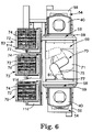
In one representative mode of operation of tool 10 shown in FIGS. 1 through 6 , a production line robot (not shown) or worker (not shown) may place a FOUP 40, which may house one or more processable substrates 74, onto one of load ports 34. Robot 62 reaches through the corresponding portal 42 to grip the FOUP 40 and brings the FOUP 40 inside buffer zone 44. In one mode of operation, the robot 62 may transfer the FOUP 40 to an open PDO assembly 54 where the FOUP operatively engages the airlock structure 59 of the PDO assembly 54. The airlock structure 59 is opened, providing egress into the FOUP 40 from inside wafer transfer system 68. In other modes, the FOUP 40 may be stored within buffer zone 44 prior to being transported to a PDO assembly 54.
As best shown by FIG. 6 , once a FOUP 40 is engaged with the airlock structure 59, wafer transfer robot 70 transfers substrates 74 from the FOUP 40 to a carrier 72 positioned at the batching station 73. Substrates 74 may be transferred to the carrier 72 in batches or one at a time. Preferably, substrates 74 are transferred one at a time. In the case of single wafer transfer, after the wafer transfer robot 70 withdraws a substrate 74, the robot 70 rotates and turns to face the batching station 73. A wrist twist operation is carried out (either clockwise or counterclockwise, as the case may be) to turn the substrate 74 from a horizontal orientation to a vertical one. The robot 70 then places the substrate 74 onto the raised elevator 102 that helps support the vertical substrate 74. The elevator 102 then lowers the substrate 102 into the carrier 72. The elevator 102 or carrier 72 may be indexed over to locate the elevator 102 with the next empty position of the carrier 72 into which another substrate 72 will be placed. The process is continued until the desired number of substrates 74 is transferred to vertical stack held in the carrier 72 at batching station 73.
Industry standard FOUP's generally can hold up to 25 processable substrates 74. However, each carrier 72 may be designed with a greater capacity, e.g., some embodiments of carriers 72 may have the ability to hold 50 or more processable substrates 74 at one time. Accordingly, substrates 74 may be batched or unbatched from such a carrier 72 to and from one or more FOUP's 40 at one or more of PDO assemblies 54.
With the carrier 72 holding the desired number of substrates 74, the carrier transport robot 76 picks up the carrier 72 and may transfer the carrier 72 either to any of buffer positions 79 and then to the hand off station 83 or directly to the hand off station 83. At the hand off station 83, processing zone robot 94 picks up the batch of substrates 74, removing them from the carrier 72 and bringing them into processing zone 84 for processing. In the meantime, the now-empty carrier 72 can be taken from the hand off position 83 and stored in wafer transfer zone 68 until needed, washed in wash station 110, or transferred directly back to the batching station 73 for additional use.
Once the processing of substrates 74 is completed in the desired manner, robot 94 returns the batch of substrates 74 to an empty carrier 72 waiting at the hand off station 83. Carrier transport robot 76 may then transfer the processed batch of substrates 74 in the carrier 72 either to a buffer position 79 and then to the batching station or directly back to the batching station 73. At the batching station 73, wafer transfer robot 70 transfers the wafers back into one or more FOUP's through one or both of PDO assemblies 54. When the unbatching is complete for each such FOUP 40, buffer zone robot 62 transfers the FOUP 40 either to a storage location and then out to a load port 34 for pick up or directly to load port 34 for pick up.
The above mode of operation was described in connection with how one batch of substrates 74 might be handled within tool 10. In actual practice, however, multiple batches will be at different stages of processing within tool 10 in order to more fully utilize the capacity of tool 10. Thus, for instance, at any one time, one batch of substrates might be undergoing loading to and/or from a carrier 72 at the batching station 73, one or more other batches might be undergoing storage on a shelf 114 or the like within wafer transfer system 68 awaiting further handling or processing, one or more batches may be undergoing storage or handling within buffer zone 44, and/or one or more other batches may be undergoing processing at stations 88, 89, and/or 90.
Other embodiments of this invention will be apparent to those skilled in the art upon consideration of this specification or from practice of the invention disclosed herein. Various omissions, modifications, and changes to the principles and embodiments described herein may be made by one skilled in the art without departing from the true scope and spirit of the invention which is indicated by the following claims.
Claims (20)
1. A wafer transfer system, the wafer transfer system comprising:
a batching station at which one or more substrates from one or more first storage devices are to be transferred to and from a second storage device, wherein said second storage device has plural substrate storage positions and said substrate storage positions are configured in a manner to store said one or more substrates in a substantially vertical orientation; and
an elevator mechanism positioned in the batching station, wherein the elevator mechanism supports the one or more substrates and is moveable to multiple positions to convey the supported one or more substrates to and from corresponding substrate holding positions of the second storage device; and
wherein the elevator mechanism comprises a rotating mechanism that engages and rotates the supported one or more substrates to a desired rotational position.
2. The wafer transfer system of claim 1 , wherein the elevator mechanism further comprises a substrate detecting sensor.
3. The wafer transfer system of claim 2 , wherein the sensor detects the one or more substrates that are stored in the second storage device from a direction that is below the one or more substrates that are stored in the second storage device.
4. The wafer transfer system of claim 1 , further comprising at least one additional elevator mechanism.
5. The wafer transfer system of claim 1 , wherein the second storage device comprises a camer.
6. The wafer transfer system of claim 5 , wherein the elevator mechanism comprises a plate having a pocket to support a substrate in a vertical orientation.
7. The wafer transfer system of claim 6 , wherein the plate has a thickness so that the plate fits between two substrates on either side of an empty substrate storage position of the carrier.
8. The wafer transfer system of claim 1 , wherein the one or more substrates are notched and the rotating mechanism engages and rotates the supported one or more substrates to a desired rotational position.
9. The wafer transfer system of claim 1 , wherein said elevator mechanism comprises multiple plates, wherein each plate has a pocket to support a corresponding substrate in a vertical orientation.
10. The wafer transfer system of claim 9 , wherein the multiple plates are integrated to cooperatively convey the supported substrates to and from corresponding substrate holding positions of the second storage device.
11. The wafer transfer system of claim 1 , wherein the elevator mechanism translates with respect to corresponding substrate holding positions of the second storage device so as to align the one or more substrates with corresponding substrate holding positions of the second storage device.
12. A method for positioning a substrates into a second storage device having plural substrate storage positions, the method comprising the steps of:
providing a first substrate on an elevator mechanism, wherein the providing step comprises:
providing the first substrate in a first storage device such that the first substrate is positioned in a horizontal orientation;
withdrawing the first substrate from the first storage device;
repositioning the substrate from the horizontal orientation to a vertical orientation; and
placing the substrate on the elevator mechanism;
positioning the elevator mechanism with respect to a desired substrate storage position of a second storage device; and
moving the elevator mechanism with respect to the second storage device so that the first substrate is transferred to the desired substrate storage position of the second storage device.
13. The method of claim 12 ,
wherein the providing step comprises providing a group of substrates on the elevator mechanism,
wherein the positioning step comprises positioning the elevator mechanism with respect to desired substrate storage positions of the second storage device, and
wherein the moving step comprises moving the elevator mechanism with respect to the second storage device so that the substrates are transferred to the desired storage positions of the second storage device.
14. The method of claim 12 , further comprising the step of repeating the providing, positioning, and moving steps with respect to the second storage device with at least one additional substrate and at least one additional substrate storage position of the second storage device.
15. The method of claim 14 ,
wherein the providing, positioning, and moving steps are repeated with respect to the second storage device with a plurality of additional substrates and a plurality of additional substrate storage positions of the second storage device such that the substrates are positioned in the second storage device;
wherein the substrates have a device side; and
wherein the device sides of the substrates are positioned in a face-to-face manner in the second storage device.
16. The method of claim 12 , wherein the first storage device comprises a FOUP.
17. The method of claim 12 , wherein the second storage device comprises a camer.
18. A method for positioning a substrate into a storage device having plural substrate storage positions, the method comprising the steps of:
providing an elevator mechanism that comprises a rotating mechanism;
providing a substrate on the elevator mechanism;
while the substrate is positioned on the elevator mechanism, using the rotating mechanism to engage and rotate the substrate to a desired rotational position; and
using an elevator mechanism to help lower the substrate into a corresponding substrate holding positions of the storage device.
19. A tool for processing microelectronic substrates, the tool comprising:
a buffer zone comprising a first storage device having one or more substrates stored in horizontal orientation;
a wafer transfer system comprising:
a batching station at which one or more substrates from the first storage device are to be transferred to and from a second storage device, wherein said second storage device has plural substrate storage positions and said substrate storage positions are configured in a manner to store said one or more substrates in a substantially vertical orientation;
an elevator mechanism positioned in the batching station, wherein the elevator mechanism supports the one or more substrates and is moveable to multiple positions to convey the supported one or more substrates to and from corresponding substrate holding positions of the second storage device; and
a wafer transfer robot that withdraws said one or more substrates from the first storage device, repositions said one or more substrates from the horizontal orientation to a vertical orientation, and places the vertically oriented one or more substrates on the elevator mechanism; and
a processing zone comprising a transfer robot that transfers the second storage device between processing zone and wafer transfer system.
20. The tool of claim 19 , wherein the elevator mechanism comprises a rotating mechanism that engages and rotates the supported one or more substrates to a desired rotational position.
Priority Applications (1)
| Application Number | Priority Date | Filing Date | Title |
|---|---|---|---|
| US10/952,506 US7134827B2 (en) | 2001-11-13 | 2004-09-28 | Reduced footprint tool for automated processing of microelectronic substrates |
Applications Claiming Priority (3)
| Application Number | Priority Date | Filing Date | Title |
|---|---|---|---|
| US33805701P | 2001-11-13 | 2001-11-13 | |
| US10/292,147 US6979165B2 (en) | 2001-11-13 | 2002-11-12 | Reduced footprint tool for automated processing of microelectronic substrates |
| US10/952,506 US7134827B2 (en) | 2001-11-13 | 2004-09-28 | Reduced footprint tool for automated processing of microelectronic substrates |
Related Parent Applications (1)
| Application Number | Title | Priority Date | Filing Date |
|---|---|---|---|
| US10/292,147 Division US6979165B2 (en) | 2001-11-13 | 2002-11-12 | Reduced footprint tool for automated processing of microelectronic substrates |
Publications (2)
| Publication Number | Publication Date |
|---|---|
| US20050063799A1 US20050063799A1 (en) | 2005-03-24 |
| US7134827B2 true US7134827B2 (en) | 2006-11-14 |
Family
ID=23323233
Family Applications (2)
| Application Number | Title | Priority Date | Filing Date |
|---|---|---|---|
| US10/292,147 Expired - Fee Related US6979165B2 (en) | 2001-11-13 | 2002-11-12 | Reduced footprint tool for automated processing of microelectronic substrates |
| US10/952,506 Expired - Fee Related US7134827B2 (en) | 2001-11-13 | 2004-09-28 | Reduced footprint tool for automated processing of microelectronic substrates |
Family Applications Before (1)
| Application Number | Title | Priority Date | Filing Date |
|---|---|---|---|
| US10/292,147 Expired - Fee Related US6979165B2 (en) | 2001-11-13 | 2002-11-12 | Reduced footprint tool for automated processing of microelectronic substrates |
Country Status (7)
| Country | Link |
|---|---|
| US (2) | US6979165B2 (en) |
| EP (1) | EP1446828A2 (en) |
| JP (1) | JP2005510055A (en) |
| KR (1) | KR20050044434A (en) |
| CN (1) | CN1608308A (en) |
| TW (1) | TW200305188A (en) |
| WO (1) | WO2003043060A2 (en) |
Cited By (3)
| Publication number | Priority date | Publication date | Assignee | Title |
|---|---|---|---|---|
| US7694688B2 (en) | 2007-01-05 | 2010-04-13 | Applied Materials, Inc. | Wet clean system design |
| US20100272544A1 (en) * | 2009-03-30 | 2010-10-28 | Ats Automation Tooling Systems Inc. | Systems and methods for handling wafers |
| US20110163065A1 (en) * | 2010-01-05 | 2011-07-07 | Applied Materials, Inc. | System for batch processing of magnetic media |
Families Citing this family (72)
| Publication number | Priority date | Publication date | Assignee | Title |
|---|---|---|---|---|
| JP2005510055A (en) | 2001-11-13 | 2005-04-14 | エフエスアイ インターナショナル インコーポレイテッド | Reduced footprint tool for automated processing of microelectronic substrates |
| US6822413B2 (en) | 2002-03-20 | 2004-11-23 | Fsi International, Inc. | Systems and methods incorporating an end effector with a rotatable and/or pivotable body and/or an optical sensor having a light path that extends along a length of the end effector |
| TWI262165B (en) * | 2002-10-16 | 2006-09-21 | Sez Ag | Device and method for transporting wafer-shaped articles |
| US6822244B2 (en) | 2003-01-02 | 2004-11-23 | Loma Linda University Medical Center | Configuration management and retrieval system for proton beam therapy system |
| TWI290901B (en) * | 2003-06-23 | 2007-12-11 | Au Optronics Corp | Warehousing conveyor system |
| WO2005013349A2 (en) * | 2003-07-31 | 2005-02-10 | Fsi International, Inc. | Controlled growth of highly uniform, oxide layers, especially ultrathin layers |
| JP4413562B2 (en) * | 2003-09-05 | 2010-02-10 | 東京エレクトロン株式会社 | Processing system and processing method |
| US20050098194A1 (en) * | 2003-09-11 | 2005-05-12 | Christenson Kurt K. | Semiconductor wafer immersion systems and treatments using modulated acoustic energy |
| US20050072625A1 (en) * | 2003-09-11 | 2005-04-07 | Christenson Kurt K. | Acoustic diffusers for acoustic field uniformity |
| US10086511B2 (en) | 2003-11-10 | 2018-10-02 | Brooks Automation, Inc. | Semiconductor manufacturing systems |
| US8696298B2 (en) * | 2003-11-10 | 2014-04-15 | Brooks Automation, Inc. | Semiconductor manufacturing process modules |
| US20070269297A1 (en) * | 2003-11-10 | 2007-11-22 | Meulen Peter V D | Semiconductor wafer handling and transport |
| US7458763B2 (en) | 2003-11-10 | 2008-12-02 | Blueshift Technologies, Inc. | Mid-entry load lock for semiconductor handling system |
| US8313277B2 (en) | 2003-11-10 | 2012-11-20 | Brooks Automation, Inc. | Semiconductor manufacturing process modules |
| US20070286710A1 (en) * | 2003-11-10 | 2007-12-13 | Van Der Meulen Peter | Semiconductor manufacturing process modules |
| JP4381121B2 (en) * | 2003-12-11 | 2009-12-09 | 大日本スクリーン製造株式会社 | Substrate processing equipment |
| EP1801869A4 (en) * | 2004-09-24 | 2010-12-08 | Hirata Spinning | Container carrying equipment |
| KR100644054B1 (en) * | 2004-12-29 | 2006-11-10 | 동부일렉트로닉스 주식회사 | Cleaning apparatus and gate oxide pre-cleaning method |
| JP4208844B2 (en) * | 2005-01-14 | 2009-01-14 | 富士通マイクロエレクトロニクス株式会社 | Exposure apparatus and control method thereof |
| JP4293150B2 (en) * | 2005-03-29 | 2009-07-08 | セイコーエプソン株式会社 | Substrate transfer device, substrate transfer method, and electro-optical device manufacturing method |
| US9159592B2 (en) | 2005-06-18 | 2015-10-13 | Futrfab, Inc. | Method and apparatus for an automated tool handling system for a multilevel cleanspace fabricator |
| US10627809B2 (en) | 2005-06-18 | 2020-04-21 | Frederick A. Flitsch | Multilevel fabricators |
| US9457442B2 (en) * | 2005-06-18 | 2016-10-04 | Futrfab, Inc. | Method and apparatus to support process tool modules in a cleanspace fabricator |
| US11024527B2 (en) | 2005-06-18 | 2021-06-01 | Frederick A. Flitsch | Methods and apparatus for novel fabricators with Cleanspace |
| US9059227B2 (en) | 2005-06-18 | 2015-06-16 | Futrfab, Inc. | Methods and apparatus for vertically orienting substrate processing tools in a clean space |
| US7513822B2 (en) * | 2005-06-18 | 2009-04-07 | Flitsch Frederick A | Method and apparatus for a cleanspace fabricator |
| US9339900B2 (en) * | 2005-08-18 | 2016-05-17 | Futrfab, Inc. | Apparatus to support a cleanspace fabricator |
| US10651063B2 (en) | 2005-06-18 | 2020-05-12 | Frederick A. Flitsch | Methods of prototyping and manufacturing with cleanspace fabricators |
| JP4767641B2 (en) * | 2005-09-27 | 2011-09-07 | 大日本スクリーン製造株式会社 | Substrate processing apparatus and substrate transfer method |
| DE102006028057B4 (en) * | 2005-10-17 | 2017-07-20 | Dynamic Microsystems Semiconductor Equipment Gmbh | Device for storing contamination-sensitive, plate-shaped objects, in particular for storing semiconductor wafers |
| KR101106203B1 (en) * | 2006-02-22 | 2012-01-20 | 가부시키가이샤 에바라 세이사꾸쇼 | Substrate processing apparatus |
| US20070231108A1 (en) * | 2006-04-04 | 2007-10-04 | Applied Materials, Inc. | Method and apparatus for transferring wafers |
| US7887280B2 (en) * | 2006-05-11 | 2011-02-15 | Tokyo Electron Limited | Processing apparatus |
| TWI452643B (en) * | 2006-05-11 | 2014-09-11 | Tokyo Electron Ltd | Inspection device and inspection method |
| US7896602B2 (en) | 2006-06-09 | 2011-03-01 | Lutz Rebstock | Workpiece stocker with circular configuration |
| US7764366B2 (en) * | 2006-07-11 | 2010-07-27 | Besi North America, Inc. | Robotic die sorter with optical inspection system |
| JP4215079B2 (en) * | 2006-07-31 | 2009-01-28 | 村田機械株式会社 | Clean stocker and article storage method |
| JP4904995B2 (en) * | 2006-08-28 | 2012-03-28 | シンフォニアテクノロジー株式会社 | Load port device |
| US7740437B2 (en) | 2006-09-22 | 2010-06-22 | Asm International N.V. | Processing system with increased cassette storage capacity |
| JP2008100805A (en) * | 2006-10-18 | 2008-05-01 | Ihi Corp | Substrate storage warehouse |
| US20080112787A1 (en) | 2006-11-15 | 2008-05-15 | Dynamic Micro Systems | Removable compartments for workpiece stocker |
| US20080138178A1 (en) * | 2006-12-06 | 2008-06-12 | Axcelis Technologies,Inc. | High throughput serial wafer handling end station |
| US7949425B2 (en) * | 2006-12-06 | 2011-05-24 | Axcelis Technologies, Inc. | High throughput wafer notch aligner |
| US8950998B2 (en) * | 2007-02-27 | 2015-02-10 | Brooks Automation, Inc. | Batch substrate handling |
| US20080206022A1 (en) * | 2007-02-27 | 2008-08-28 | Smith John M | Mult-axis robot arms in substrate vacuum processing tool |
| US20080206036A1 (en) * | 2007-02-27 | 2008-08-28 | Smith John M | Magnetic media processing tool with storage bays and multi-axis robot arms |
| US20080219807A1 (en) * | 2007-03-05 | 2008-09-11 | Van Der Meulen Peter | Semiconductor manufacturing process modules |
| US7585142B2 (en) * | 2007-03-16 | 2009-09-08 | Asm America, Inc. | Substrate handling chamber with movable substrate carrier loading platform |
| US20080310939A1 (en) * | 2007-06-15 | 2008-12-18 | Taiwan Semiconductor Manufacturing Company, Ltd. | System and method for use in a lithography tool |
| KR100887161B1 (en) * | 2007-08-03 | 2009-03-09 | 주식회사 에이디피엔지니어링 | Plasma treatment apparatus |
| JP4989398B2 (en) * | 2007-09-27 | 2012-08-01 | 大日本スクリーン製造株式会社 | Substrate processing equipment |
| KR101647277B1 (en) * | 2008-02-05 | 2016-08-10 | 다이나믹 마이크로시스템즈 세미컨덕터 이큅먼트 게엠베하 | Automatic handling buffer for bare stocker |
| US9633881B2 (en) * | 2008-02-05 | 2017-04-25 | Brooks Automation, Inc. | Automatic handling buffer for bare stocker |
| US8070410B2 (en) * | 2008-02-05 | 2011-12-06 | Lutz Rebstock | Scalable stocker with automatic handling buffer |
| DE102008009090B3 (en) * | 2008-02-14 | 2009-06-04 | MAG Industrial Automation Systems, LLC., Sterling Heights | Loading and unloading system for machine tools |
| WO2010008929A1 (en) * | 2008-07-15 | 2010-01-21 | Ulvac, Inc. | Work-piece transfer systems and methods |
| US9048274B2 (en) * | 2008-12-08 | 2015-06-02 | Taiwan Semiconductor Manufacturing Co., Ltd. | Portable stocker and method of using same |
| JP5083221B2 (en) * | 2009-01-05 | 2012-11-28 | パナソニック株式会社 | Pallet automatic changer |
| JP4973675B2 (en) * | 2009-02-26 | 2012-07-11 | 東京エレクトロン株式会社 | Substrate processing apparatus and substrate processing method |
| AT510516B1 (en) * | 2010-09-21 | 2013-10-15 | Trumpf Maschinen Austria Gmbh | MANUFACTURING CELL WITH A COMPONENT TRANSFER DEVICE AND TRANSPORT DEVICE FOR PARTS AND SPACERS |
| US20120306139A1 (en) | 2011-06-03 | 2012-12-06 | Arthur Keigler | Parallel single substrate processing system holder |
| CN103295931A (en) * | 2012-02-29 | 2013-09-11 | Lgcns株式会社 | Providing device and method of LED wafers |
| US9045827B2 (en) * | 2012-03-09 | 2015-06-02 | Lg Cns Co., Ltd. | Apparatus and method for supplying light-emitting diode (LED) wafer |
| US9136149B2 (en) | 2012-11-16 | 2015-09-15 | Taiwan Semiconductor Manufacturing Company, Ltd. | Loading port, system for etching and cleaning wafers and method of use |
| CN104813438B (en) | 2012-11-28 | 2017-07-25 | 盛美半导体设备(上海)有限公司 | The cleaning method and device of semi-conductor silicon chip |
| KR102075528B1 (en) * | 2013-05-16 | 2020-03-03 | 삼성디스플레이 주식회사 | Deposition apparatus, method for manufacturing organic light emitting display apparatus, and organic light emitting display apparatus |
| US9378992B2 (en) | 2014-06-27 | 2016-06-28 | Axcelis Technologies, Inc. | High throughput heated ion implantation system and method |
| KR102160106B1 (en) * | 2014-07-03 | 2020-09-25 | 세메스 주식회사 | Apparatus for transferring a wafer |
| CN105278259A (en) * | 2015-07-27 | 2016-01-27 | 江苏影速光电技术有限公司 | Stand-alone double-table and multi-station automatic printed circuit board (PCB) exposure equipment and exposure method |
| US9607803B2 (en) | 2015-08-04 | 2017-03-28 | Axcelis Technologies, Inc. | High throughput cooled ion implantation system and method |
| JP6705668B2 (en) * | 2016-03-11 | 2020-06-03 | ファスフォードテクノロジ株式会社 | Die bonding apparatus and semiconductor device manufacturing method |
| GB2610156A (en) * | 2021-04-29 | 2023-03-01 | Edwards Ltd | Semiconductor processing system |
Citations (31)
| Publication number | Priority date | Publication date | Assignee | Title |
|---|---|---|---|---|
| US4568234A (en) | 1983-05-23 | 1986-02-04 | Asq Boats, Inc. | Wafer transfer apparatus |
| JPS63303060A (en) | 1987-05-30 | 1988-12-09 | Tokuda Seisakusho Ltd | Vacuum treatment equipment |
| EP0308275A2 (en) | 1987-09-18 | 1989-03-22 | Varian Associates, Inc. | Sputter module for modular wafer processing machine |
| US5064337A (en) | 1988-07-19 | 1991-11-12 | Tokyo Electron Limited | Handling apparatus for transferring carriers and a method of transferring carriers |
| US5217501A (en) | 1989-07-25 | 1993-06-08 | Tokyo Electron Limited | Vertical wafer heat treatment apparatus having dual load lock chambers |
| US5376212A (en) | 1992-02-18 | 1994-12-27 | Tokyo Electron Yamanashi Limited | Reduced-pressure processing apparatus |
| US5378145A (en) | 1992-07-15 | 1995-01-03 | Tokyo Electron Kabushiki Kaisha | Treatment system and treatment apparatus |
| US5435683A (en) | 1991-03-26 | 1995-07-25 | Tokyo Electron Limited | Load-lock unit and wafer transfer system |
| US5468112A (en) * | 1992-10-05 | 1995-11-21 | Tokyo Electron Limited | Wafer container and wafer aligning apparatus |
| US5544421A (en) | 1994-04-28 | 1996-08-13 | Semitool, Inc. | Semiconductor wafer processing system |
| US5620295A (en) * | 1990-11-17 | 1997-04-15 | Tokyo Electron Limited | Transfer apparatus |
| WO1998002910A1 (en) | 1996-07-15 | 1998-01-22 | Semitool, Inc. | Automated semiconductor processing systems |
| WO1999002436A1 (en) | 1997-07-11 | 1999-01-21 | Asyst Technologies, Inc. | Smif pod storage, delivery and retrieval system |
| WO1999062107A1 (en) | 1998-05-27 | 1999-12-02 | Varian Semiconductor Equipment Associates, Inc. | Batch end effector for semiconductor wafer handling |
| WO2000002675A1 (en) | 1998-07-08 | 2000-01-20 | Semitool, Inc. | Automated semiconductor processing system |
| US6071059A (en) * | 1995-03-28 | 2000-06-06 | Brooks Automation Gmbh | Loading and unloading station for semiconductor processing installations |
| US6203268B1 (en) * | 1996-04-24 | 2001-03-20 | Tokyo Electron Limited | Positioning apparatus for substrates to be processed |
| US6235634B1 (en) | 1997-10-08 | 2001-05-22 | Applied Komatsu Technology, Inc. | Modular substrate processing system |
| US6290405B1 (en) | 1999-06-01 | 2001-09-18 | Tokyo Electron Limited | Substrate processing apparatus |
| US6313903B1 (en) | 1999-02-01 | 2001-11-06 | Tokyo Electron Limited | Resist coating and developing unit |
| US6318944B1 (en) * | 1995-06-15 | 2001-11-20 | Kokusai Electric Co., Ltd. | Semiconductor fabricating apparatus, method for modifying positional displacement of a wafer in a wafer cassette within the semiconductor fabricating apparatus and method for transferring the wafer cassette |
| US6344126B1 (en) | 1999-08-30 | 2002-02-05 | Micron Technology, Inc. | Electroplating apparatus and method |
| US6365033B1 (en) | 1999-05-03 | 2002-04-02 | Semitoof, Inc. | Methods for controlling and/or measuring additive concentration in an electroplating bath |
| US6376261B1 (en) | 2000-01-03 | 2002-04-23 | Advanced Micro Devices Inc. | Method for varying nitride strip makeup process based on field oxide loss and defect count |
| US6413356B1 (en) * | 2000-05-02 | 2002-07-02 | Applied Materials, Inc. | Substrate loader for a semiconductor processing system |
| US6444481B1 (en) | 2001-07-02 | 2002-09-03 | Advanced Micro Devices, Inc. | Method and apparatus for controlling a plating process |
| US20030091410A1 (en) | 2001-11-13 | 2003-05-15 | Larson Robert E. | Reduced footprint tool for automated processing of microelectronic substrates |
| US6572320B2 (en) | 1997-05-05 | 2003-06-03 | Semitool, Inc. | Robot for handling workpieces in an automated processing system |
| US6663332B1 (en) | 1998-01-27 | 2003-12-16 | Asm International N.V. | System for the treatment of wafers |
| US6705828B2 (en) | 1995-07-19 | 2004-03-16 | Hitachi, Ltd. | Vacuum processing apparatus and semiconductor manufacturing line using the same |
| US6755603B2 (en) * | 1998-02-18 | 2004-06-29 | Tokyo Electron Limited | Apparatus for and method of transporting substrates to be processed |
Family Cites Families (2)
| Publication number | Priority date | Publication date | Assignee | Title |
|---|---|---|---|---|
| AU2429395A (en) * | 1994-04-28 | 1995-11-29 | Semitool, Incorporated | Semiconductor processing systems |
| US6852644B2 (en) * | 2002-11-25 | 2005-02-08 | The Boc Group, Inc. | Atmospheric robot handling equipment |
-
2002
- 2002-11-08 JP JP2003544796A patent/JP2005510055A/en not_active Withdrawn
- 2002-11-08 WO PCT/US2002/035998 patent/WO2003043060A2/en not_active Application Discontinuation
- 2002-11-08 KR KR1020047007232A patent/KR20050044434A/en not_active Application Discontinuation
- 2002-11-08 EP EP02789550A patent/EP1446828A2/en not_active Withdrawn
- 2002-11-08 CN CNA028260678A patent/CN1608308A/en active Pending
- 2002-11-12 US US10/292,147 patent/US6979165B2/en not_active Expired - Fee Related
- 2002-11-12 TW TW091133135A patent/TW200305188A/en unknown
-
2004
- 2004-09-28 US US10/952,506 patent/US7134827B2/en not_active Expired - Fee Related
Patent Citations (32)
| Publication number | Priority date | Publication date | Assignee | Title |
|---|---|---|---|---|
| US4568234A (en) | 1983-05-23 | 1986-02-04 | Asq Boats, Inc. | Wafer transfer apparatus |
| JPS63303060A (en) | 1987-05-30 | 1988-12-09 | Tokuda Seisakusho Ltd | Vacuum treatment equipment |
| EP0308275A2 (en) | 1987-09-18 | 1989-03-22 | Varian Associates, Inc. | Sputter module for modular wafer processing machine |
| US5064337A (en) | 1988-07-19 | 1991-11-12 | Tokyo Electron Limited | Handling apparatus for transferring carriers and a method of transferring carriers |
| US5217501A (en) | 1989-07-25 | 1993-06-08 | Tokyo Electron Limited | Vertical wafer heat treatment apparatus having dual load lock chambers |
| US5620295A (en) * | 1990-11-17 | 1997-04-15 | Tokyo Electron Limited | Transfer apparatus |
| US5435683A (en) | 1991-03-26 | 1995-07-25 | Tokyo Electron Limited | Load-lock unit and wafer transfer system |
| US5376212A (en) | 1992-02-18 | 1994-12-27 | Tokyo Electron Yamanashi Limited | Reduced-pressure processing apparatus |
| US5378145A (en) | 1992-07-15 | 1995-01-03 | Tokyo Electron Kabushiki Kaisha | Treatment system and treatment apparatus |
| US5468112A (en) * | 1992-10-05 | 1995-11-21 | Tokyo Electron Limited | Wafer container and wafer aligning apparatus |
| US5544421A (en) | 1994-04-28 | 1996-08-13 | Semitool, Inc. | Semiconductor wafer processing system |
| US6071059A (en) * | 1995-03-28 | 2000-06-06 | Brooks Automation Gmbh | Loading and unloading station for semiconductor processing installations |
| US6318944B1 (en) * | 1995-06-15 | 2001-11-20 | Kokusai Electric Co., Ltd. | Semiconductor fabricating apparatus, method for modifying positional displacement of a wafer in a wafer cassette within the semiconductor fabricating apparatus and method for transferring the wafer cassette |
| US6705828B2 (en) | 1995-07-19 | 2004-03-16 | Hitachi, Ltd. | Vacuum processing apparatus and semiconductor manufacturing line using the same |
| US6203268B1 (en) * | 1996-04-24 | 2001-03-20 | Tokyo Electron Limited | Positioning apparatus for substrates to be processed |
| WO1998002910A1 (en) | 1996-07-15 | 1998-01-22 | Semitool, Inc. | Automated semiconductor processing systems |
| US6572320B2 (en) | 1997-05-05 | 2003-06-03 | Semitool, Inc. | Robot for handling workpieces in an automated processing system |
| WO1999002436A1 (en) | 1997-07-11 | 1999-01-21 | Asyst Technologies, Inc. | Smif pod storage, delivery and retrieval system |
| US6235634B1 (en) | 1997-10-08 | 2001-05-22 | Applied Komatsu Technology, Inc. | Modular substrate processing system |
| US6663332B1 (en) | 1998-01-27 | 2003-12-16 | Asm International N.V. | System for the treatment of wafers |
| US6755603B2 (en) * | 1998-02-18 | 2004-06-29 | Tokyo Electron Limited | Apparatus for and method of transporting substrates to be processed |
| WO1999062107A1 (en) | 1998-05-27 | 1999-12-02 | Varian Semiconductor Equipment Associates, Inc. | Batch end effector for semiconductor wafer handling |
| WO2000002675A1 (en) | 1998-07-08 | 2000-01-20 | Semitool, Inc. | Automated semiconductor processing system |
| US6313903B1 (en) | 1999-02-01 | 2001-11-06 | Tokyo Electron Limited | Resist coating and developing unit |
| US6365033B1 (en) | 1999-05-03 | 2002-04-02 | Semitoof, Inc. | Methods for controlling and/or measuring additive concentration in an electroplating bath |
| US6290405B1 (en) | 1999-06-01 | 2001-09-18 | Tokyo Electron Limited | Substrate processing apparatus |
| US6344126B1 (en) | 1999-08-30 | 2002-02-05 | Micron Technology, Inc. | Electroplating apparatus and method |
| US6376261B1 (en) | 2000-01-03 | 2002-04-23 | Advanced Micro Devices Inc. | Method for varying nitride strip makeup process based on field oxide loss and defect count |
| US6413356B1 (en) * | 2000-05-02 | 2002-07-02 | Applied Materials, Inc. | Substrate loader for a semiconductor processing system |
| US6444481B1 (en) | 2001-07-02 | 2002-09-03 | Advanced Micro Devices, Inc. | Method and apparatus for controlling a plating process |
| WO2003043060A2 (en) | 2001-11-13 | 2003-05-22 | Fsi International, Inc. | Reduced footprint tool for automated processing of substrates |
| US20030091410A1 (en) | 2001-11-13 | 2003-05-15 | Larson Robert E. | Reduced footprint tool for automated processing of microelectronic substrates |
Non-Patent Citations (1)
| Title |
|---|
| International Search Report for PCT/US02/35998 mailed Oct. 10, 2003. |
Cited By (5)
| Publication number | Priority date | Publication date | Assignee | Title |
|---|---|---|---|---|
| US7694688B2 (en) | 2007-01-05 | 2010-04-13 | Applied Materials, Inc. | Wet clean system design |
| US20100272544A1 (en) * | 2009-03-30 | 2010-10-28 | Ats Automation Tooling Systems Inc. | Systems and methods for handling wafers |
| US9184079B2 (en) * | 2009-03-30 | 2015-11-10 | Ats Automation Tooling Systems Inc. | Systems and methods for handling wafers |
| US20110163065A1 (en) * | 2010-01-05 | 2011-07-07 | Applied Materials, Inc. | System for batch processing of magnetic media |
| US8911554B2 (en) * | 2010-01-05 | 2014-12-16 | Applied Materials, Inc. | System for batch processing of magnetic media |
Also Published As
| Publication number | Publication date |
|---|---|
| US20030091410A1 (en) | 2003-05-15 |
| TW200305188A (en) | 2003-10-16 |
| EP1446828A2 (en) | 2004-08-18 |
| US20050063799A1 (en) | 2005-03-24 |
| JP2005510055A (en) | 2005-04-14 |
| US6979165B2 (en) | 2005-12-27 |
| KR20050044434A (en) | 2005-05-12 |
| WO2003043060A2 (en) | 2003-05-22 |
| WO2003043060A3 (en) | 2003-11-27 |
| CN1608308A (en) | 2005-04-20 |
Similar Documents
| Publication | Publication Date | Title |
|---|---|---|
| US7134827B2 (en) | Reduced footprint tool for automated processing of microelectronic substrates | |
| US6822413B2 (en) | Systems and methods incorporating an end effector with a rotatable and/or pivotable body and/or an optical sensor having a light path that extends along a length of the end effector | |
| US11587816B2 (en) | Container storage add-on for bare workpiece stocker | |
| US10672633B2 (en) | Removable compartments for workpiece stocker | |
| US7604449B1 (en) | Equipment front end module | |
| EP1094921B1 (en) | Transferring substrates with different holding end effectors | |
| US8292563B2 (en) | Nonproductive wafer buffer module for substrate processing apparatus | |
| US7976263B2 (en) | Integrated wafer transfer mechanism | |
| US8812150B2 (en) | Semiconductor manufacturing process modules | |
| US20090028669A1 (en) | Removable compartments for workpiece stocker | |
| EP1252079B1 (en) | Wafer transport system | |
| EP2092556B1 (en) | Compartments for workpiece stocker | |
| WO2001040085A1 (en) | Small footprint carrier front end loader | |
| EP1460676A2 (en) | Reduced footprint tool for automated processing of microelectronic substrates |
Legal Events
| Date | Code | Title | Description |
|---|---|---|---|
| CC | Certificate of correction | ||
| REMI | Maintenance fee reminder mailed | ||
| LAPS | Lapse for failure to pay maintenance fees | ||
| STCH | Information on status: patent discontinuation |
Free format text: PATENT EXPIRED DUE TO NONPAYMENT OF MAINTENANCE FEES UNDER 37 CFR 1.362 |
|
| FP | Lapsed due to failure to pay maintenance fee |
Effective date: 20101114 |